MAA50-2K4812SBP中文资料
BAC4812 蓄电池充电器 用户手册说明书

BAC4812蓄电池充电器用户手册郑州众智科技股份有限公司ZHENGZHOU SMARTGEN TECHNOLOGY CO.,LTD.目 次前言 (3)1概述 (4)2性能特点 (4)3充电原理 (4)4参数规格 (5)5设置 (6)5.1电压调节 (6)5.2电流调节 (6)6操作说明 (6)7外形及安装尺寸 (7)前 言是本公司的中文商标是本公司的英文商标SmartGen―smart的意思是灵巧的、智能的、聪明的,gen是generator(发电机组)的缩写,两个单词合起来的意思是让发电机组变得更加智能。
不经过本公司的允许,本文档的任何部分不能被复制(包括图片及图标)。
本公司保留更改本文档内容的权利,而不通知用户。
公司地址:中国.河南省郑州市高新技术产业开发区金梭路28号电话:+86-371-67988888+86-371-67981888+86-371-67991553+86-371-67992951+86-371-67981000(外贸)全国免费电话:400-0318-139传真:+86-371-67992952网址://邮箱:*****************表1版本发展历史日期版本内容2016-06-24 1.0开始发布1概述BAC4812系列蓄电池充电器采用最新开关电源器件,专门针对发动机起动用的铅酸蓄电池的充电特性而设计,适合铅酸电池的长期补充充电(浮充)。
此款充电器适用于12V蓄电池组充电,其最大充电电流为3A。
2性能特点产品有以下特点:a)采用开关电源式结构,输入电压范围宽,体积小,重量轻,效率高。
b)采用二阶段充电法(即先恒流后恒压方式)自动充电,充分按照蓄电池充电特性进行充电,可防止铅酸蓄电池过充电,能最大程度提高电池寿命。
c)具有辅助电压输出口,稳定输出-12V电压。
d)+12V输出具有短路及接反保护功能。
e)-12V输出具有短路自恢复功能。
f)充电电压、电流值均可在现场通过电位器调节。
MCP4822

5V 交流 / 直流特性
电气特性:除非另有说明,否则,所有参数符合以下条件:VDD = 5V, AVSS = 0V, VREF = 2.048V,输出缓冲器增益 (G) = 2x, RL = 5 kΩ 连接到地, CL = 100 pF, TA = -40 至 +85°C。典型值为 +25°C 时测得。 参数 电源要求 输入电压 输入电流 - MCP4821 I Cur - MCP4822 硬件关断电流 软件关断电流 上电复位门限 直流精度 分辨率 INL 误差 DNL (注 1) 失调误差 失调误差温度系数 增益误差 增益误差温度系数 内部电压基准 (VREF) 标称基准电压 温度系数 (注 1) n INL DNL VOS VOS/°C gE 12 -12 -0.75 -1 — — -2 — 2.008 — — — — 输出噪声 (VREF 噪声) 输出噪声密度 ENREF (0.1-10 Hz) eNREF (1 kHz) eNREF (10 kHz) 1/f 转折频率 注 fCORNER 1: 设计参数,未经产品测试。 2: 信号太小而未测试。 — — — — — 2 ±0.2 ±0.02 0.16 -0.44 -0.10 -3 2.048 125 0.25 45 0.09 290 1.2 1.0 400 — 12 +0.75 1 — — 2 — 2.088 325 0.65 160 0.32 — — — — 位 LSb LSb % FSR ppm/°C ppm/°C % FSR ppm/°C V ppm/°C LSb/°C ppm/°C LSb/°C µVp-p µV/√Hz µV/√Hz Hz VOUTA,当 G = 1x 且代码 = 0xFFFh -40°C 至 0°C -40°C 至 0°C 0°C 至 +85°C 0°C 至 +85°C 代码 = 0xFFFh, G = 1 代码 = 0xFFFh, G = 1 代码 = 0xFFFh, G = 1 器件为单调性 代码 = 0x000h -45°C 至 25°C +25°C 至 85°C 代码 0xFFFh,不包括失调误差 VDD IDD ISHDN ISHDN_SW VPOR 2.7 — — — — — — 330 415 0.3 3.3 2.0 5.5 400 750 2 6 — µA µA µA V 数字输入连接到地,输出未加负载, 代码 = 0x000 符号 最小值 典型值 最大值 单位 测试条件
AO4822A中文资料

SymbolTyp Max 4862.574110R θJL 3540Maximum Junction-to-Lead CSteady-State°C/WThermal Characteristics ParameterUnits Maximum Junction-to-Ambient A t ≤ 10s R θJA °C/W °C/W Maximum Junction-to-Ambient A Steady-State AO4822AAO4822ASymbolMin TypMaxUnits BV DSS 30V 1T J =55°C5I GSS 100nA V GS(th)1 1.73V I D(ON)30A 13.416T J =125°C202519.526m Ωg FS 23S V SD 0.751V I S3A C iss 9551250pF C oss 145pF C rss 112pF R g0.50.85ΩQ g (10V)1724nC Q g (4.5V)912nC Q gs 3.4nC Q gd 4.7nC t D(on)56.5ns t r 67.5ns t D(off)1925ns t f 4.56ns t rr 16.721ns Q rr6.710nCTHIS PRODUCT HAS BEEN DESIGNED AND QUALIFIED FOR THE CONSUMER MARKET. APPLICATIONS OR USES AS CRITICAL COMPONENTS IN LIFE SUPPORT DEVICES OR SYSTEMS ARE NOT AUTHORIZED. AOS DOES NOT ASSUME ANY LIABILITY ARISING OUT OF SUCH APPLICATIONS OR USES OF ITS PRODUCTS. AOS RESERVES THE RIGHT TO IMPROVE PRODUCT DESIGN,FUNCTIONS AND RELIABILITY WITHOUT NOTICE.Maximum Body-Diode Continuous CurrentInput Capacitance Output Capacitance Turn-On DelayTime DYNAMIC PARAMETERS V GS =10V, V DS =15V, I D =8.5ATotal Gate Charge Gate Drain Charge V GS =0V, V DS =15V, f=1MHz SWITCHING PARAMETERS Turn-On Rise Time Turn-Off DelayTime V GS =10V, V DS =15V, R L =1.8Ω, R GEN =3ΩTurn-Off Fall TimeTotal Gate Charge Gate Source Charge Gate resistanceV GS =0V, V DS =0V, f=1MHzm ΩV GS =4.5V, I D =6AI S =1A,V GS =0V V DS =5V, I D =8.5AR DS(ON)Static Drain-Source On-ResistanceForward TransconductanceDiode Forward VoltageI DSS µA Gate Threshold Voltage V DS =V GS I D =250µA V DS =24V, V GS =0VV DS =0V, V GS = ±20V Zero Gate Voltage Drain Current Gate-Body leakage current Electrical Characteristics (T J =25°C unless otherwise noted)STATIC PARAMETERS Parameter Conditions Body Diode Reverse Recovery Time Body Diode Reverse Recovery ChargeI F =8.5A, dI/dt=100A/µsDrain-Source Breakdown Voltage On state drain currentI D =250µA, V GS =0V V GS =10V, V DS =5V V GS =10V, I D =8.5AReverse Transfer Capacitance I F =8.5A, dI/dt=100A/µs A: The value of R θJA is measured with the device mounted on 1in 2 FR-4 board with 2oz. Copper, in a still air environment with T A =25°C. The value in any given application depends on the user's specific board design. The current rating is based on the t ≤ 10s thermal resistance rating.B: Repetitive rating, pulse width limited by junction temperature.C. The R θJA is the sum of the thermal impedence from junction to lead R θJL and lead to ambient.D. The static characteristics in Figures 1 to 6 are obtained using 80 µs pulses, duty cycle 0.5% max.E. These tests are performed with the device mounted on 1 in 2FR-4 board with 2oz. Copper, in a still air environment with T A =25°C. The SOA curve provides a single pulse rating. Rev 0: Aug 2005AO4822AAO4822A。
mcp4822-中文
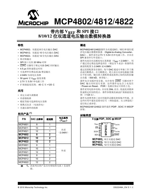
应用
• • • • • 设定点或失调微调 传感器校准 精度等级可选择的电压基准 便携式仪表 (电池供电) 光通信器件的校准
相关产品 (1)
P/N MCP4801 MCP4811 MCP4821 MCP4802 MCP4812 MCP4822 MCP4901 MCP4911 MCP4921 MCP4902 MCP4912 MCP4922 注 DAC 分辨率 8 10 12 8 10 12 8 10 12 8 10 12 通道数 1 1 1 2 2 2 1 1 1 2 2 2 外部 内部 (2.048V) 电压基准 (VREF)
ISHDN_SW VPOR
— —
5 1.85
— —
µA V
n INL DNL n INL DNL n INL DNL VOS VOS/°C gE G/°C VREF VREF/°C
8 — — 10 — — 12 — — — — — — — — — — —
— ±0.25 ±0.2 — ±1 ±0.2 — ±4 ±0.25 ±0.02 -5 -0.10 -3 2.048 125 0.25 45 0.09 290 1.2 1.0 400
ISHDN_SW VPOR
— —
3.3 2.0
6 —
µA V
n INL DNL n INL DNL n INL DNL VOS VOS/°C gE G/°C
8 -1 -0.5 10 -3.5 -0.5 12 -12 -0.75 -1 — — -2 —
— ±0.125 ±0.1 — ±0.5 ±0.1 — ±2 ±0.2 ±0.02 0.16 -0.44 -0.10 -3
<10 45 <10 <10
— — — —
850封口机说明书
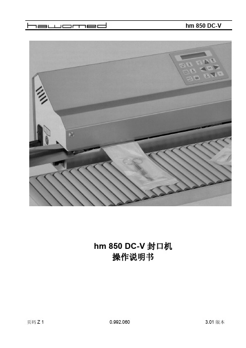
hm 850 DC-V 封口机 操作说明书
页码 Z 1
0.992.060
3.01 版本
中文
hm 850 DC-V
目录
中文
1 引言 ...................................................................................................................................................................... 3 1.1 前言 ................................................................................................................................................................... 3 1.2 符号说明............................................................................................................................................................ 3 1.3 重要提示............................................................................................................................................................ 4 1.4 安全提示.............
4812说明书
简介谢谢您购买绿扬牌YB4812型晶体管特性图示仪。
为保证正确利用,请在利用前认真阅读此说明书.阅毕,请将说明书保留好。
该图示仪依照严格的质量操纵标准生产,元器件进行了全面的挑选老化。
售后效劳:若是显现任何故障,请与咱们的销售部或各维修点联系,以取得快捷而有效的售后效劳。
注意:该仪器必需在规定的工作环境中利用,才能保证其处于最正确工作状态。
警示:电源插头应有接地爱惜,改换保险丝时应断开输入电源。
非专业技术人员请勿打开盖板。
1.概述YB4812型晶体管特性图示仪是一种用于测量各类半导体管特性曲线和静态参数的测量仪器。
本仪器是新一代便携式图示仪,整机采纳新颖电路设计技术,除具有一般图示仪的功能外,还具有外形轻巧、操作简便、性能稳固靠得住、性价比高的特点,能知足大部份半导体器件的测试要求。
适合于工厂生产线、大专院校、仪器修理业等领域。
2.要紧技术指标Y轴系统集电极电流范围(Ic):10μA/div~div,分14档,误差不超过±5%。
扩展×10,误差不超过±10%。
X轴系统集电极电压范围(Vc):div~50V/div,分10档,误差不超过±5%。
基极电压范围(Vbe):~div,分4档,误差不超过±5%。
阶梯信号阶梯电流范围:5μA/div~10mA/div,分11档,误差不超过±5%。
阶梯电压范围:~,分4档,误差不超过±5%。
每簇级数:0~10级持续可调。
串联电阻:0、10kΩ,误差不超过±10%。
集电极扫描电源峰值电压:0~50V、0~500V持续可调。
电流容量:0~50V 2A;0~500V 500mA。
功耗限制电阻:约0~100kΩ持续可调。
容性电流:500V时小于5μA。
其他示波管:15SJ118Y-14(内)。
外型尺寸:430mm×320mm×150mm (D×B×H)。
MAA50-2S481212SBP中文资料

Single-output modelsModule МАА50- 1S03S ХХ МАА50- 1S05S ХХ МАА50- 1S12S ХХ МАА50- 1S15S ХХ МАА50- 1S24S ХХ МАА50- 1S27S ХХМАА50- 1S48S ХХ МАА50- 1S68S ХХ Output power 26,4 W 40 W 50 W Output voltage 3,3 VDC 5 VDC12 VDC15 VDC24 VDC27 VDC48 VDC68 VDCOutput current8 A8 А 4,17 А 3,33 А 2,27 А 1,85 А 1,04 А 0,73 АDual-output modelsModule МАА50-2S0505S ХХ МАА50-2S1212S ХХМАА50-2S1515S ХХOutput power 50 WChannel number 1 2 1 2 1 2 Output voltage 5 VDC 5 VDC 12 VDC 12 VDC15 VDC 15 VDC Output current5 А 5 А 2,1 А 2,1 А 1,67 А 1,67 АTriple-output modelsModule МАА50-3S051212S ХХМАА50-3S051515S ХХOutput power 50 WChannel number 1 2 3 1 2 3Output voltage 5 VDC12 VDC12 VDC5 VDC15 VDC15 VDCOutput current5 А 1,04А 1,04А 5 А 0,83 А 0,83 Аby request can be delivered modules with non-standard output voltage from 3 to 70 VDC and maximal output current to 8А.Ordering informationМАА 50 – 3 S 05 15 15 S U Nc d e f g h i j k lc - MAA Seriesd - Nominal output power, Watte - Channel quantity (1, 2, 3)f - - Input voltageS – 220VAC K – 115VACg - Output voltage channel 1, VDC h - Output voltage channel 2, VDC i - Output voltage channel 3, VDC j - Execution with sealing k - EmbodimentB – uniform case with primingl - Operating temperature range of caseN - - 40°С…+85°С P - - 50°С…+85°С• Rugged environment in operation intechnical equipment of industrial and special purpose. • Low-profile construction • Metal case• Cooling by heat sink or free air convection• Electromagnetic compatibility index to GOST V 25803-91 for group 1.2.1 (curve 2) • Stability to external factors of group 1U GOST RV 20.39.414.1-97 (additional) • Short circuit protection, overload, overvoltage and thermal protection • Galvanic isolated outputs •Acceptance «5»Температура окружающей среды Токр, С9080706050403020100-10-20-30-40-50Выходная мощность, Вт6050403020100Input specificationsParameter Conditions of dimensions MIN NOM MAX UnitS 187 220 242 VACSteady-state deviationК 80 115 140 VAC S 176 264 VACInput voltageTransient deflection, 1 secК 80 150 VAC SInput frequencyК47 400 440 HzOutput specificationsParameterConditions of dimensions MIN NOM MAX Unit Single-output execution (Inom 10 – 100%) ±3 % Output 1 multi-output execution(Inom 10 – 100%) ±3 %Uout2&3 differs from Uout1 less than 20% Output 2 and 3 multi-output execution(Inom 10 – 100%)±13 %Output 1 multi-output execution (Inom 30 – 100%) ±3 %Total output voltage instabilityUout2&3differs fromUout1 more than 20% Output 2 and 3 multi-output execution(Inom 50-100%) ±15 %Output voltage pulsations ripple(peak-to-peak)Dimension by device for pulsation control2% Uout.nom.Current overload protection actuation level110 % Iout.nom. Short circuit protection Autorepair 150 % Iout.nom. Overvoltage protection 120 % Uout.nom.Thermal protection90-95°CGeneral specificationsParameterConditions of dimensions MIN NOM MAX Unit- operating of case N P – 40 – 50 +85+85°C– power loss See diagram Temperature– storage – 50 +85 °CEfficiency 78 % Conversion frequency 50 kHz~ in/out 1500 VAC ~ in/case 1500 VAC~ out/case 500 VDC Isolation~ out/out 500 VDCInsulation resistance Voltage 500VDC 20 Ohm High humidity Temperature 35°С 98 % Cyclic overpatching of temperature – 60 +85 °C Multiple mechanical shocks Speeding-up 15g 2 15 ms Sinusoidal vibration Speeding-up 5g 50 500 Hz Atmosphere pressure 6х104 1,2х105 Pa Time to failure Temperature 35°C 105 hour Mass 0,4 kg all specifications redused for normal climatic conditions, Uin.nom., Iout.nom., if it is not specified differently.Power loss diagramFree airconvectionWith heat sinkAmbient temperature Tamb, °CO u t p u t p o w e r , WOutput settings№ pin1 2 3 4 5 6 7 8 9 Single-channel case ~IN (N) ~IN (L) +out1 +out1 +out1 -out1 -out1 -out1 Dual-channel case ~IN (N) ~IN (L) +out1 +out1 -out1 -out1 -out2 +out2 Triple-channelcase~IN (N)~IN (L)-out3+out3+out1-out1-out2+out2Switching on standart diagramFU in – current safety device 1A for input voltage 220VAC, 2A for input voltage 115VAC.S out – ceramic condenser capacity 0,47-15 mcF with corresponding operating voltage to decrease high-frequency noise level.S out2 – electronic condenser capacity 22-100 mcF in consideration with operating voltage and polarity. It makes for purpose to decrease dynamic instability when module work at dynamic load.+Out -Out ~In (L) ~In (N) Power module R heat CaseСout1 Сout2~In (L)~In (N)ground FU inSingle, Dual, and Triple-output execution SBNSingle, Dual, and Triple-output execution SVN (with flexible erection joints)The Flexible erection fjoints by length (100±5)mm is executed by wire section (0,5...1,5)mm2.。
mos管4812
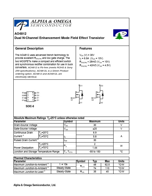
SymbolTyp Max 4862.574110R θJL3540Maximum Junction-to-Lead CSteady-State°C/WParameterUnits Maximum Junction-to-Ambient A t ≤ 10s R θJA °C/W Maximum Junction-to-Ambient A Steady-State °C/W Thermal Characteristics AO4812SymbolMin TypMaxUnits BV DSS 30V 0.0041T J =55°C5I GSS 100nA V GS(th)1 1.93V I D(ON)20A 22.528T J =125°C31.33834.542m Ωg FS 1015.4S V SD 0.761V I S3A C iss 680820pF C oss 102pF C rss 77pF R g3 3.6ΩQ g (10V)13.8417nC Q g (4.5V) 6.748.1nC Q gs 1.82nC Q gd 3.2nC t D(on) 4.67ns t r 4.1 6.2ns t D(off)20.630ns t f 5.27.5ns t rr 16.520ns Q rr7.810nCTHIS PRODUCT HAS BEEN DESIGNED AND QUALIFIED FOR THE CONSUMER MARKET. APPLICATIONS OR USES AS CRITICAL COMPONENTS IN LIFE SUPPORT DEVICES OR SYSTEMS ARE NOT AUTHORIZED. AOS DOES NOT ASSUME ANY LIABILITY ARISING OUT OF SUCH APPLICATIONS OR USES OF ITS PRODUCTS. AOS RESERVES THE RIGHT TO IMPROVE PRODUCT DESIGN,FUNCTIONS AND RELIABILITY WITHOUT NOTICE.Body Diode Reverse Recovery TimeBody Diode Reverse Recovery Charge Turn-Off Fall TimeSWITCHING PARAMETERS Total Gate Charge Total Gate Charge Gate Source Charge Turn-On DelayTime V GS =10V, V DS =15V, R L =2.2Ω, R GEN =3ΩV GS =10V, V DS =15V, I D =6.9AGate Drain Charge Reverse Transfer Capacitance Turn-On Rise Time Turn-Off DelayTime Gate resistanceV GS =0V, V DS =0V, f=1MHzForward TransconductanceV DS =5V, I D =6.9ADiode Forward Voltage I S =1A Maximum Body-Diode Continuous CurrentDYNAMIC PARAMETERS Input Capacitance V GS =0V, V DS =15V, f=1MHz Output Capacitance R DS(ON)Static Drain-Source On-ResistanceV GS =10V, I D =6.9Am ΩV GS =4.5V, I D =5.0AGate Threshold Voltage V DS =V GS I D =250µA On state drain currentV GS =4.5V, V DS =5V V DS =24V, V GS =0VµA Gate-Body leakage current V DS =0V, V GS =±20V I F =6.9A, dI/dt=100A/µsI F =6.9A, dI/dt=100A/µsElectrical Characteristics (T J =25°C unless otherwise noted)ParameterConditions STATIC PARAMETERS Drain-Source Breakdown Voltage I D =250µA, V GS =0V I DSS Zero Gate Voltage Drain Current A: The value of R θJA is measured with the device mounted on 1in 2FR-4 board with 2oz. Copper, in a still air environment with T A =25°C. The value in any given application depends on the user's specific board design. The current rating is based on the t ≤ 10s thermal resistance rating.B: Repetitive rating, pulse width limited by junction temperature.C. The R θJA is the sum of the thermal impedence from junction to lead R θJL and lead to ambient.D. The static characteristics in Figures 1 to 6 are obtained using 80 µs pulses, duty cycle 0.5% max.E. These tests are performed with the device mounted on 1 in 2FR-4 board with 2oz. Copper, in a still air environment with T A =25°C. The SOA curve provides a single pulse rating. Rev 4 : Sept 2005TYPICAL ELECTRICAL AND THERMAL CHARACTERISTICS。
MAX4820中文资料

*For maximum heat dissipation, packages have an exposed pad (EP) on the bottom. Solder exposed pad to GND.
Pin Configurations
TOP VIEW
20 SET 19 VCC 18 OUT1 17 OUT2 16 PGND
RESET 1 CS 2 DIN 3
SCLK 4 DOUT 5
MAX4820
15 OUT3 14 OUT4 13 COM 12 OUT5 11 OUT6
N.C. 6 GND 7 OUT8 8 OUT7 9 PGND 10
SPI and QSPI are trademarks of Motorola, Inc. MICROWIRE is a trademark of National Semiconductor Corp.
PIN-PACKAGE
MAX4820ETP*
-40°C to +85°C 20 Thin QFN-EP
MAX4820EUP*
-40°C to +85°C 20 TSSOP
MAX4821ETP*
-40°C to +85°C 20 Thin QFN-EP
MAX4821EUP*
-40°C to +85°C 20 TSSOP
The MAX4820/MAX4821 8-channel relay drivers offer built-in kickback protection and drive +3.3V/+5V nonlatching or dual-coil-latching relays. These devices are especially useful when driving +3V relays. Each independent open-drain output features a 2Ω on-resistance and is guaranteed to sink 70mA (min) of load current. Both devices consume less than 50µA (max) quiescent current and have 1µA output off-leakage current. The MAX4820 features an SPI™-/QSPI™-/MICROWIRE™compatible serial interface. Input data is shifted into an 8bit shift register and latched to the outputs when CS transitions from low to high. Each data bit in the shift register corresponds to a specific output, allowing independent control of all outputs. The MAX4821 features a 4-bit (A0, A1, A2, LVL) parallel-input interface. The first three bits (A0, A1, A2) determine the output address, and the fourth bit (LVL) determines whether the selected output is switched on or off. Data is latched to the outputs when CS transitions from low to high. Both devices feature separate set and reset functions that allow the user to turn on or turn off all outputs simultaneously with a single control line. Built-in hysteresis (Schmidt trigger) on all digital inputs allows this device to be used with slow rising and falling signals, such as those from optocouplers or RC power-up initialization circuits. The MAX4820/MAX4821 are available in 20-pin TSSOP and space-saving 20-pin thin QFN packages.
电源适配器 MA1210 用户手册说明书

用户手册电源适配器MA1210规格参数参数项参数内容170-240VAC 50Hz AC输入尺寸使用环境内直径2.1毫米,外直径5.5毫米DC插头工作温度:-30~50℃、存储温度:-40~70℃工作湿度:10%~90%RH不凝结、存储湿度:5%~90%RH不凝结DC输出12VDC 1A(MAX)80mmX132mmX33mm注意:此为A级产品,在生活环境中,该产品可能会造成无线电干扰。
在这种情况下,可能需要客户对干扰采取切实可行的措施。
按电源内盒卡扣,取出内盒。
①③将监控摄像机的DC电源线与稳压电源DC接口连接,线头保持安全距离,以防短路。
④将电源内盒推入外壳中,确认锁紧,并⑤通过壁挂孔将电源安装在合适的位置。
物品清单:电源适配器 x 6 说明书 x 1②根据不同布线需求,选择合适的操作方式。
7108502529 REV1.0.4有毒有害物质含量声明产品保修卡下列情况不属于免费维修范围,深圳市美科星通信技术有限公司(以下简称本公司)可提供有偿服务,请注意:未按使用说明书要求安装、使用、维护、保管导致的产品故障或损坏;已经超出保修、保换期限;擅自涂改、撕毁产品条形码;产品保修卡上的产品条形码或型号与产品本身不符;未经本公司许可,擅自改动产品固有的设置文件或擅自拆机修理;意外因素或人为行为导致的产品故障或损坏,如对准强光聚焦、输入不合适电压、高温、进水、机械破坏、摔坏、产品严重氧化或生锈等;产品在客户发回返修途中由于运输、装卸所导致的损坏;因不可抗力如地震、火灾、水灾、雷击等导致的产品故障或损坏;其他非产品本身设计、技术、制造、质量等问题而导致的产品故障或损坏。
特别说明:在国家法律法规的范围内,本承诺的解释权、修改权归深圳市美科星通信技术有限公司。
电源适配器的保换期限为1年,电池的保换期限为6个月。
如因用户使用不当或意外因素,造成电源适配器或电池有明显的硬物损伤、裂痕、断脚、严重变形,电源线破损、断线、裸芯等现象则不予保换,用户可另行购买。
D4812中文资料
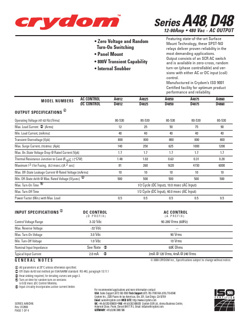
Series A48, D48 12-90Amp • 480 Vac - AC OUTPUT
• Zero Voltage and Random Turn-On Switching • Panel Mount • 800V Transient Capability • Internal Snubber
MOUNTING HOLE/SLOT 0.17 (4.3) DIA.
1.10 (27.9)
.45 (11.4)
FASTON TERMINAL .250 X .032 (2 PLCS.)
.87 REF. (22.2)
Crydom Heat Sinks offer excellent thermal management and are perfectly matched to the load current ratings of Crydom panel mount relays. Request Crydom’s Heat Sink specification sheet for all the details.
Crydom Inc., 2320 Paseo de las Americas, Ste. 201, San Diego, CA 92154
Email: sales@ WEB SITE:
SERIES A48/D48.
UK: +44 (0)1202 606030 • FAX +44 (0)1202 606035 Crydom SSR Ltd., Arena Business Centre,
A4850 D4850
A4875 D4875
A4890 D4890
Operating Voltage (47-63 Hz) [Vrms]
MEMORY存储芯片RT4812GJ8F中文规格书
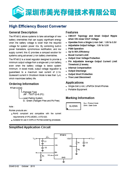
General Description
The RT4812 allows systems to take advantage of new battery chemistries that can supply significant energy when the battery voltage is lower than the required voltage for system power ICs. By combining built-in power transistors, synchronous rectification, and low supply current; this IC provides a compact solution for systems using advanced Li-Ion battery chemistries. The RT4812 is a boost regulator designed to provide a minimum output voltage from a single-cell Li-Ion battery, even when the battery voltage is below system minimum. In boost mode, output voltage regulation is guaranteed to a maximum load current of 2.1A. Quiescent current in Shutdown Mode is less than 1A, which maximizes battery life.
OCP The converter senses the current signal when the high-side P-MOSFET turns on. As a result, the OCP is cycle by-cycle current limitation. If the OCP occurs, the converter holds off the next on pulse until inductor current drops below the OCP limit.
MA3100类II过流保护器商品说明书

Class IIIClass II 100kA* (10/350µs)5kA (8/20µs)*Total over a 3 phase systemCascade Effect Examplestandalone device and in cascade coordination with Class I lightning arrester. A single width module withstands surge currents up to 40,000A with an 8/20µs waveform. Class I I arresters are available in single width modules for maximum user flexibility, double width modules for all-mode protection on single phase systems and quad width modules for all-mode protection on three phase systems. The Class II modules have remote monitoring capabilities as a standard feature. Voltage free, normally open, normally closed contacts can beused for a variety of monitoring tasks.The MA3145 Class II surge current arrestor has a Short CircuitCurrent rating (SCCR) of 200kA which removes the need for externalfusing and reduces installation cost.The MA3100 range offers cost effective surge protection for applications described by IEC 61312, where the AC mains supply can carry a partial share of the lightning surge current. Class I surge protectors (rated according to IEC 61643) are designed to carry up to 50kA (10/350µs). Class II surge protectors are characterized by their ability to protect against 8/20µs impulses up to 40kA, possibly resulting from the operation of a class I device. Finally Class III devices are used to protect individual pieces of equipment. An excellent example of a class III device is the MA15.Coordinated IEC 61643 Class I, Class II and Class III surge protectionEaton Electric Limited,Great Marlings, Butterfield, Luton Beds, LU2 8DL, UK.Tel: + 44 (0)1582 723633 Fax: + 44 (0)1582 422283E-mail:********************© 2016 EatonAll Rights ReservedPublication No. EPS 901-173 RevC September 20161TN-C-S SystemVariations for IT ORMA3145-230-1-R MA3145-230-2-RMA3145-230-1-R Variations for TTT o order Class II surge protection devices, specify -R = Remote contacts present MA31 = (Product range name)120 = operating voltage 230 = operating voltage 1 = 1 module width 2 = 2 module widths 45 = Product rangeFigure 1 Class II dimensionsBA Class II Surge Protection DeviceT echnical dataDimensions (see Fig. 1 for A and B)IEC category/VDE requirement class:Nominal voltage U n :Max. continuous operating voltage U Lightning test current Iimp (10/350µs)Test standards: UL1449 3rd Edition; IEC 61643-11:2011-03MA3145-230-1-REUROPE (EMEA): +44 (0)1582 723633 ********************THE AMERICAS: +1 800 835 7075*********************ASIA-PACIFIC: +65 6 645 9888***********************The given data is only intended as a productdescription and should not be regarded as a legal warranty of properties or guarantee. In the interest of further technical developments, we reserve the right to make design changes.Eaton Electric Limited,Great Marlings, Butterfield, Luton Beds, LU2 8DL, UK.Tel: + 44 (0)1582 723633 Fax: + 44 (0)1582 422283E-mail:********************© 2016 EatonAll Rights ReservedPublication No. EPS 901-173 RevC 190916September 20162MTL MA3145 (I & II Pole) Class IISeptember 2016。
新马电池公司 PM 系列电源模块产品说明书
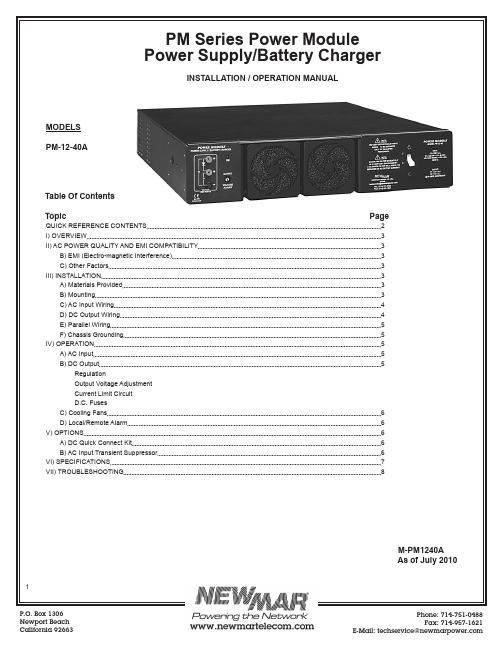
1PM Series Power ModulePower Supply/Battery ChargerINSTALLATION / OPERATION MANUALMODELSPM-12-40ATable Of ContentsTopic PageQUICK REFERENCE CONTENTS 2I) OVERVIEW 3II) AC POWER QUALITY AND EMI COMPATIBILITY 3B) EMI (Electro-magnetic Interference) 3C) Other Factors 3III) INSTALLATION 3A) Materials Provided 3B) Mounting 3C) AC Input Wiring 4D) DC Output Wiring 4E) Parallel Wiring 5F) Chassis Grounding 5IV) OPERATION 5A) AC Input 5B) DC Output 5RegulationOutput Voltage AdjustmentCurrent Limit CircuitD.C. FusesC) Cooling Fans 6D) Local/Remote Alarm 6V) OPTIONS 6A) DC Quick Connect Kit 6B) AC Input Transient Suppressor 6VI) SPECIFICATIONS 7VII) TROUBLESHOOTING 8M-PM1240AAs of July 20102Quick Reference ContentsThe front and rear panel features of the Power Modules are illustrated below, along with the page number where information on eachparticular feature is located.Figure 1: Power Module Front PanelPM “ON”Indicator LED,Pg. 5Cooling Fans,Pg. 6Input Switch/Circuit Breaker,Pg. 5Output VoltageTest Points,Pg. 5Output VoltageAdjustment Pot,Pg. 5,6Figure 2: Power Module Rear PanelA.C. Input Socket,Pg. 4Output Terminals,Pg. 4Wiring Access Port,Chassis Grounding Stud,Pg. 5Remote Alarm Contacts,Pg. 63I) OverviewThe PM Series Power Module is a uniquely adaptable communicationequipment power source which functions as either power supply or batterycharger for 12 volt d.c. systems positive, negative or floating ground.Power Modules may be employed singly or in combina t ion. Units maybe paral l eled for N + 1 redundancy and alarm contacts allow local orremote mon i toring. An optional d.c. wiring quick connect kit allows easyreplacement of modules while the system as a whole remains up andrunning (see section V-B).Power Modules may be used separately as a power source, or they maybe integrated with NEWMAR’s Power Function Manager (model PFM-400;rated to 400 amps maximum) to greatly expand the system capability withother functions such as digital output monitoring, multiple load distributionand low voltage disconnect. (Contact the factory for complete informationregarding the PFM-400.) Note: If the Power Module is being installedas part of an integrated system with the PFM-400 refer to the manualwhich comes with that unit for all d.c. wiring instructions and functionaldescriptions.II) AC Power Quality and EMI CompatibilityA) AC Power QualityReliability is of prime concern when designing an AC-DC powersystem for communication sites. Poor AC input power qualitycan seriously impede system reliability. In particular, transientdisturbances on the power lines can severely weaken or causefailure of semi-conductors in power supplies and communicationgear. It is important that you know the input power quality wheninstalling the PM. Following is some basic information on thesubject:CausesTransients are characterized as a voltage pulse of high energy and veryshort duration impressed upon the AC wave form. These over voltagepulses can range from 1 to 100 times the normal AC voltage level and canlast for a fraction of a cycle to a few cycles.Transient disturbances can be placed into two categories:- Lightning generated- Equipment generatedA direct lightning hit on a utility power line will cause a high energy voltagetransient to travel in both directions along the power line. This disturbancecan affect equipment hundreds of miles from the strike point.Equipment generated transient sources include utility fault conditionsand load switching as well as on-site equipment such as pumps and airconditioning loads, motors, phase control equipment.RecommendationsAll PM models are designed to meet IEEE 587/ANSI C62.41 requirementsfor transient withstand capability. The AC power source should conform tothis specification to ensure reliable power supply operation.If the power source quality is suspect or unknown, it is recommended thatan AC power quality survey be conducted by a power quality consultantor power conditioning firm. Corrective measures may include lightningsuppressors, line conditioners and filters.An optional AC transient suppressor (see OPTIONS section) isrecommended for installations in third world countries and sites that aresubject to nearby lightning strikes or transients caused by nearby motorcontactors, air conditioning compressors, etc.B) EMI (Electro-Magnetic Interference) ConsiderationsThe PM Series Power Modules employ switch-mode technology to con-vert AC to DC. They are designed to produce minimal EMI levels whenoperating (compliant to International Standards EN55022 [conducted]and EN50082 [immunity]). Although the level of EMI produced may beacceptable for most radio applications, some installations may not eventolerate what little EMI is produced.Analog microwave and other extremely sensitive radio sites mayrequire additional input/output filtering and careful installation. In somecases linear power supplies (also available from NEWMAR) should beconsidered, as they emit lower EMI (although they are more susceptible to“brown-outs” or voltage sags and high input voltage).C) Other FactorsSome of the various factors which must be considered when discussingelectrical interference include the following:- RF Signal strength- Ground loops- Power and signal cable routing proximity- Power supply and radio mounting locations- Antenna, signal, and power groundsIII) InstallationA) Materials ProvidedPrior to installation, check to ensure that each of the following items havebeen included with the packaging. For any missing items please contactthe factory or warehouse.(2) ea. mounting brackets for 19” rack mounting (# 13917-0)(2) ea. mounting brackets for 23” rack mounting (# 13918-0)(6) ea. 6-32 X 3/8” pan head phillips screws(1) ea. Molex “pigtail” connector(1) ea. IEC 115V NEMA 5-15P AC input power cord(1) ea. Installation/Operation manual(1) ea. Output terminal coverB) MountingThe PM is provided with two pairs of mounting ears: one for 19” rackmounting (# 13917-0) and one for 23” rack mounting (# 13918-0). Six #6-32 x 3/8” pan head Phillips screws are provided for attaching the earsto the PM chassis. Select the appropriate set of ears and fasten to the PMsides.Note there are three sets of a triangular pattern of 6-32 tapped holeson each side of the PM. When rack mounting (two posts) the PM it isrecommended that the ‘center mount’ holes (6” set back from the PM’sfront panel) be used. The set of holes nearest the front panel and theset nearest the rear panel are normally used when installing the optionalUniversal Mounting Bracket (UMB).For four post mounting, please contact the factory for a second set of ears(specify 19” or 23” and the model no.), mount one pair of ears to the frontholes and the second pair of ears to the center or rear most tapped holes.Adjust your cabinet rail front to back distance so it matches the mountingholes on the PM.4Note: Due to the weight of the Power Module, we do not recommend flush mounting the PM with the mounting ears attached to the forward most mounting holes unless rear support is provided.C) AC Input WiringInput Wiring: PM-12-40A is provided with an IEC power cord (in theinstallation kit) with a NEMA 5-15 plug for a 115V AC outlet on one end and a molded socket at the other which fits the entry module at the rear of the PM. If the 5-15 plug is not suited to the available AC outlet, 1) obtain an IEC cord with appropriate plug or 2) cut off the 5-15 plug, obtain the correct plug for the outlet and attach it to the provided IEC cord. (Plug should be rated at 15 amps minimum). When replacing the plug, pay careful attention to the pin wiring as follows:Brown.........................AC Hot (over-current protected) Blue............................AC NeutralGreen*........................AC Ground (safety, earth) * may be Green with Yellow StripeInput Voltage Selection: The PM-12-40A is universal input. No switch required and will accept input of 90-264 VAC, 47-63 Hz.Important: Although the internal AC wiring is protected by the front panel mounted circuit breaker, the wiring to the PM must also be protected by plugging into an appropriate over-current protected three prong outlet or routed through a separate dedicated fuse or circuit breaker on an AC distribution panel with proper safety/earth chassis ground in accordance with all applicable codes and ordinances.Distribution Panel AC Fuse/Circuit Breaker Values 15 ampCAUTION (230 V a.c applications only): If AC input is derived from a source consisting of two HOT leads (phase-to-phase 230V AC inputvoltage), an external fuse or circuit breaker (double pole) must be used to protect the unfused (formerly NEUTRAL, now HOT) lead.D) DC Output WiringIMPORTANT: Ensure that AC input to the PM is switched off beforeworking with DC wiring. The output terminals are “hot” whenever the unit is switched on.1) Output terminals for hard-wiring of DC output are located on the rear panel of the PM. Terminate wires with 1/4” ring lug connectors for a secure installation.2) Use the chart below to determine minimum gauge for wires depend-ing on the particular model and the length of the run from the PM to the load or distribution bus (or refer to N.E.C or local codes for any questions regarding proper DC wire gauges):DC Wire Size Table:Model Minimum Wire Size per N.E.C. AWG (mm) PM-12-40A: #8 (10 mm)To minimize line loss at lengths greater than 5 feet, it is recommended to increase wire size one gauge for each additional 5 feet of cable run.3) Two separate (+) output terminals are provided. Connection of d.c. wiring is typically made to the (-) output and the “V OUT” (+) output ter-minal, though “V2” (+) may be used instead if the application requires it (see “V2” below).“V OUT” (+) Terminal: This output is routed through an internal “or-ing”/isolation diode. This terminal should be used for most installations. Use of this terminal is mandatory when the PM is wired for parallel n+1 redundant operation, or when it is used as a battery charger. Regula t ion at this terminal is 2 % line/load. Note: When the PM is used in a parallel n+1 redundant configuration, output current is derated by 10 % due to current sharing tolerances (see SPECIFICATIONS section).“V2” (+) Terminal: This is a direct output without the internal oring/isolation diode in line. 1 % regulation is available at this terminal and it should only be used in installations where only a single PM is used, 1 % regulation is required and the PM will not be wired to a battery. Output voltage measured at this terminal is approximately 0.7V d.c. higher than at the “V OUT” terminal.Typical single PM wiring schemes are illustrated in Figures 5-6.FIGURE 5: Single Power Module, negative ground, with battery:Figure 6: Single Power Module, negative ground, no battery, 1% regulation required:(-) Negative to Load or Ground Bus Bar(+) Positive to Load or Distribution Panel>>(+) Positive to Load or Distribution Panel(-) Negative to Load or Ground Bus Bar5E) Parallel WiringThe internal oring/isolation diode of the PM allows parallel n+1 redundant wiring with no modification or other external isolation de v ices required. Figure 9 on the following page illustrate some typical parallel wiring schemes.IMPORTANT: When wiring two or more units in parallel d.c. wires for all units should be identical in gauge and length and the output voltage of each module should be adjusted (as outlined below) in order to facilitate droop load sharing.Parallel Load Sharing Adjustment Procedures Method 1:1) Shut off all but one of the Power Modules and apply a load equivalent to 1/2 of the rating for that unit (e.g., for model PM-12-40A apply a 20 amp load).2) Connect a digital voltmeter to the test points on the front of the power module at the “V OUT” and (+) and (-) positions.3) Verify that the output voltage is at the correct factory setting (see Specifications section) or at the desired system voltage. If adjustment is neces s ary, use a small flat tip screwdriver to turn the “OUTPUT VOLTAGE ADJUST” potentiometer on the front panel until the voltmeter reads the desired system output voltage.4) Shut off the PM, turn on the next unit in the system, and repeat steps 2 through 4 until all PM’s in the system have the identical “V OUT” output voltage.Method 2:1) With all Power Modules powered up, apply the typical operational d.c. system load.2) Using a clamp-on ammeter, measure the output current of each PM in the system. If there is an out-put current differential of greater than 5 % between any two PM’s, attach the ammeter to the PM with the highest output current and turn the “OUTPUT VOLTAGE ADJUST” potentiometer on that unit slowly counterclockwise, until the output current of that unit reduces slightly.3) Repeat step 2 until there is less than 5 % current output differential between all PM’s in the system.F) Chassis GroundingIf grounding of the PM chassis is required for theinstallation, use the provided 1/4” grounding stud on the rear panel for this purpose (see Figure 2 or 3).FIGURE 6: Parallel (two to three Power Modules) and N+1 redundancy, negative ground V) Operation A) AC InputThe PM will operate on 90-264 VAC input at 47-63 Hz. No input voltage selection or adjustment is required for 115/230 VAC, 50 or 60 Hz. operation.AC input is protected against over-current and internal short circuit condi t ions by the circuit breaker/input power switch on the front panel. When this switch is in the on position and DC is available at the output terminal, the “ON” indicator L.E.D. on the left side of the front panel will illuminate.B) DC OutputThe PM produces 12 VDC nominal output. The ground reference may be positive, negative or floating.Regulation: Regulation at the “V OUT” output terminal is within ± 2 % of rated voltage, under all line and load conditions. Regulation at the “V2” terminal is ± 1 %. Ripple is within ± 1 % of rated voltage with or without batteries on-line.Output Voltage Adjust: Factory-set voltages (as measured at the V OUT terminal) and approximate adjustment ranges are specified below. Adjust m ent is made at the “OUTPUT VOLTAGE ADJUST” pot on the left side of the front panel using a small flat tip screwdriver (see Figure 1). Output voltage test points for both the “V OUT” and “V2” outputs areprovided beside the voltage adjust pot for ease of monitoring while making this adjustment. Use of a digital multimeter is recommended when making this adjustment. If the PM has had the charger function board installed, output voltage adjustments are automatic and this adjustment pot is disabled.••••○○>(+) Positive to Distribution Panel or Battery (fuse at battery per N.E.C. or local codes)Power Module #1Power Module #2Power Module #3<<<(-) Negative to Loads or BatteryIf the battery is connected to the PM output with backwards polarity, the fuses should blow to protect DC wiring. However damage to internal components may also have occurred. If the replacement fuse blows, return To maximize the life of the internal components and to allow continu o us operation at full rating, the PM employs automatic cooling fans. These fans operate at full speed whenever AC is applied and the unit is producing DCPreventative Maintenance: The fan is a maintenance-free ball-bearing type and does not require lubrication. It is equipped with a filter to keep Relay contact rating for all models is 5a @ 30V DC V) Options (Available from the Factory)UnusedPositionsUnusedPositions7The suppressor provides continuous bi-polar, bi-directional, non-inter-rupting protection for both the PM and load from damaging high voltage transients. It is installed in-line with AC input to the PM. Status indicators verify input and “PROTECTED” conditions and alarm contacts indicate when the unit has tripped and equipment is in the unprotected mode. Two models are available for 115V and 230V applications. Contact the factory for more information on how to obtain this transient suppressor.VI) SPECIFICATIONSAll ModelsInput: 90-264 VAC, 47-63 Hz.Power Factor: .96-.99Regulation: ± 2% at V OUT (through “oring” diode)Ripple P-P: 1%Efficiency: 80-85% @ full loadOutput Voltage Adjustment Range: ± 10 %Temperature Rating: 0° to +60° C derate linearly from 100% load @ 50° C to 80% load at 60° CAltitude Operational Rating: Full output to 5,000 feet; reduce output current 4% per 1,000 feetabove 5,000 feet; 10,000 feet maximumIndividual Model Specifications† For parallel configuration/load sharing derate output 10%ProtectionOutput fuse for reverse polarityCurrent limit and foldbackInput circuit breakerAutomatic high temperature protectionCase Size:3.5” H x 17” W* x 20.5” D* 19” and 23” mounting brackets providedCertifications• EN 55022 (Conducted)• FCC Part 15, Level A (Radiated)Model Input OutputRecommended Weight Amps V OUT V2Amps Battery Lbs Kg. @ F.L. Cont.† Capacity115/230V (Amp/Hours)*PM-12-40 8.5/4.3 13.6 14.3 40 80-40012.2 5.5 PM-12-70 16/8 13.6 14.3 70140-70015.2 6.9 PM-24-20 8.5/4.3 27.2 27.9 2040-20012.2 5.5 PM-24-35 16/8 27.2 27.9 3570-35015.2 6.9 PM-48-10 8.5/4.3 54.4 55.1 1018-9012.2 5.5 PM-48-18 16/8 54.4 55.1 1836-18014.0 6.48A. No output currentB. PM repeatedly trips input circuitbreaker with no battery or loadconnectedC. Reverse polarity batteryconnection to PM has caused PM tostop chargingD. High output voltage measuredacross “V OUT” terminalsE. Batteries connected to PMovercharging1. Using a voltmeter, confirm AC input volt a ge.Check input connections.2. Reduce DC load and/or determine cause ofover temperature condition.3. Clear or replace clogged fan filter. Removefan obstruction, or replace fan if necessary. (Seesection IV-D, Cooling Fans)4. Replace blown fuse (See section IV-B, DCOutput.)5. Return to place of purchase for repair/re-placement or contact NEWMAR for returnauthorization.Return to place of purchase for repair/re p lacementor contact NEWMAR for return authorization.Replace output fuses. If fuses blow again, return toplace of purchase for repair/re p lacement or contactNEWMAR for return authorization.Check for tight connection of charging leads fromPM to batteries.1. Move positive output wire from “V2” position to“V OUT” position.2. Lower output voltage (See section IV-B, DCOutput.) to battery manufacturer’s recommendedcharging voltageVII) TroubleshootingCondition Solution Possible Cause1. PM not receiving AC input voltage or is notreceiving correct input voltage2. PM limiting its output due to overload orambient over temperature condition3. One or both fans not operating properly,or filter clogged, causing over temperaturecondition and PM power reduction4. Blown output fuses5. Defective Power ModuleInternal shortDC output fuses and possibly other compo-nents blownBatteries not connected to PM. It is normal toread 1/2 volt higher across “V OUT” terminalswith no battery connected1. Batteries connected to “V2” output terminals.“V2” output is approximately .7 volt higher than“V OUT” output2. Output voltage adjusted too high。
八马电池参数

八马电池参数八马电池是一种常见的锂电池,广泛应用于电动汽车、电动自行车、储能系统等领域。
它具有高能量密度、长寿命、轻巧、低自放电率等优点。
下面,我将详细介绍八马电池的参数。
一、额定电压:八马电池的额定电压通常为3.6V。
这是锂电池的一般标准电压,符合大多数应用场景的需求。
二、容量:八马电池的容量根据型号和用途的不同,通常在1000mAh至3000mAh之间。
容量越大,电池的使用时间就越长,但同时也会增加电池的尺寸和重量。
三、尺寸和重量:八马电池的尺寸和重量也多样化,以适应不同应用场景的需求。
一般来说,电池的尺寸越小,重量越轻,越适合用于便携设备和轻量化设备。
四、充电电压和放电电压:八马电池的充电电压通常为4.2V,放电电压为3.0V。
在充放电过程中,需要严格控制电压,以确保电池的安全性和使用寿命。
五、充电温度和放电温度:八马电池的充电温度通常在0°C至45°C之间,放电温度在-20°C至60°C之间。
超出这个温度范围,电池的性能可能会受到影响,并可能造成电池的损坏。
六、循环寿命:八马电池具有较长的循环寿命,一般可以达到数百个充放电循环。
这意味着电池可以进行多次充放电,使用寿命较长,更经济实用。
七、自放电率:八马电池的自放电率较低,一般为每月1%-2%左右。
这意味着即使在长时间不使用的情况下,电池的电量也能够保持较长时间,不会产生明显的电量损失。
八、安全性能:八马电池具有良好的安全性能,采用了多种安全保护措施,如过充保护、过放保护、过流保护等,以确保电池在使用过程中的安全性和可靠性。
九、环保性:八马电池是一种绿色环保产品,不含汞、镉、铅等有害物质,符合环保要求,并且可以进行循环利用。
总结起来,八马电池具有高能量密度、长寿命、轻巧、低自放电率等优点,适用于电动汽车、电动自行车、储能系统等领域。
同时,它也具备良好的安全性能和环保性,为用户提供安全可靠的能源解决方案。
mos管4812

SymbolTyp Max 4862.574110R θJL3540Maximum Junction-to-Lead CSteady-State°C/WParameterUnits Maximum Junction-to-Ambient A t ≤ 10s R θJA °C/W Maximum Junction-to-Ambient A Steady-State °C/W Thermal Characteristics AO4812SymbolMin TypMaxUnits BV DSS 30V 0.0041T J =55°C5I GSS 100nA V GS(th)1 1.93V I D(ON)20A 22.528T J =125°C31.33834.542m Ωg FS 1015.4S V SD 0.761V I S3A C iss 680820pF C oss 102pF C rss 77pF R g3 3.6ΩQ g (10V)13.8417nC Q g (4.5V) 6.748.1nC Q gs 1.82nC Q gd 3.2nC t D(on) 4.67ns t r 4.1 6.2ns t D(off)20.630ns t f 5.27.5ns t rr 16.520ns Q rr7.810nCTHIS PRODUCT HAS BEEN DESIGNED AND QUALIFIED FOR THE CONSUMER MARKET. APPLICATIONS OR USES AS CRITICAL COMPONENTS IN LIFE SUPPORT DEVICES OR SYSTEMS ARE NOT AUTHORIZED. AOS DOES NOT ASSUME ANY LIABILITY ARISING OUT OF SUCH APPLICATIONS OR USES OF ITS PRODUCTS. AOS RESERVES THE RIGHT TO IMPROVE PRODUCT DESIGN,FUNCTIONS AND RELIABILITY WITHOUT NOTICE.Body Diode Reverse Recovery TimeBody Diode Reverse Recovery Charge Turn-Off Fall TimeSWITCHING PARAMETERS Total Gate Charge Total Gate Charge Gate Source Charge Turn-On DelayTime V GS =10V, V DS =15V, R L =2.2Ω, R GEN =3ΩV GS =10V, V DS =15V, I D =6.9AGate Drain Charge Reverse Transfer Capacitance Turn-On Rise Time Turn-Off DelayTime Gate resistanceV GS =0V, V DS =0V, f=1MHzForward TransconductanceV DS =5V, I D =6.9ADiode Forward Voltage I S =1A Maximum Body-Diode Continuous CurrentDYNAMIC PARAMETERS Input Capacitance V GS =0V, V DS =15V, f=1MHz Output Capacitance R DS(ON)Static Drain-Source On-ResistanceV GS =10V, I D =6.9Am ΩV GS =4.5V, I D =5.0AGate Threshold Voltage V DS =V GS I D =250µA On state drain currentV GS =4.5V, V DS =5V V DS =24V, V GS =0VµA Gate-Body leakage current V DS =0V, V GS =±20V I F =6.9A, dI/dt=100A/µsI F =6.9A, dI/dt=100A/µsElectrical Characteristics (T J =25°C unless otherwise noted)ParameterConditions STATIC PARAMETERS Drain-Source Breakdown Voltage I D =250µA, V GS =0V I DSS Zero Gate Voltage Drain Current A: The value of R θJA is measured with the device mounted on 1in 2FR-4 board with 2oz. Copper, in a still air environment with T A =25°C. The value in any given application depends on the user's specific board design. The current rating is based on the t ≤ 10s thermal resistance rating.B: Repetitive rating, pulse width limited by junction temperature.C. The R θJA is the sum of the thermal impedence from junction to lead R θJL and lead to ambient.D. The static characteristics in Figures 1 to 6 are obtained using 80 µs pulses, duty cycle 0.5% max.E. These tests are performed with the device mounted on 1 in 2FR-4 board with 2oz. Copper, in a still air environment with T A =25°C. The SOA curve provides a single pulse rating. Rev 4 : Sept 2005TYPICAL ELECTRICAL AND THERMAL CHARACTERISTICS。
CDMA BTS 4812T 简介

CDMA BTS 4812T 简介目录1CDMA BTS 4812T 基本介绍 (2)1.1信道处理器机架 (2)1.2信道处理器机架C-CCP的介绍 (2)1.2信道处理器机架 (3)1.2主要控制板卡功能简介 (3)1.3基站顶部的介绍 (8)2BTS基站上电前的准备 (12)2.1基站接地检查 (12)2.2基站上电检查 (12)2.3CSM 系统GPS的跟踪 (13)2.4Span检测 (15)1 CDMA BTS 4812T 基本介绍1.1 信道处理器机架信道处理器机架C-CCP 的介绍1) 信道处理器机架(C-CCP )中安装基站的各种控制板卡,如(图3-1)所示。
图3-1信道处理器机架中各种控制板卡的安装位置示意图2) 处理器机架图信道处理器机架主要由以下控制板卡:a) PS-1,PS-2 - 电源模块 b) GLI2 - 接口板 c) CIO - 输出输入合成板 d) CCD - 时钟处理板 e) HSO - 高稳晶振 f) AMR - 告警板 g) CSM - GPS 接收处理 h) MCC24 – 24路语音处理板 i) MCC8 - 8路语音处理板 j) BBX2 - 宽带收发处理板 k) Switch – 板卡切换控制 l) MPC - 话路预选控制器1.2信道处理器机架主要控制板卡功能简介1)GLI2的功能GLI2的功能相当于整个BTS的控制器。
它提供了话音和信令的路由,对信道处理器机架“C-CCP”中的所有板卡进行管理。
(1)GLI2提供了BTS与CBSC的SPAN的接口。
(2)GLI2提供了BTS与外部设备连接的网口(LAN A和LAN B)。
如LMF的接入端口。
(3)GLI2提供了一个MMI口,用操作系统中的Hyper Terminal可以接入。
且通过MMI,维护人员可以对GLI2和SPAN的各种状态进行监控和设置。
a)GLI2板卡上的指示灯状态及含义在GLI2有五个指示灯,一个“RESET”按钮和一个“MMI”接口。
- 1、下载文档前请自行甄别文档内容的完整性,平台不提供额外的编辑、内容补充、找答案等附加服务。
- 2、"仅部分预览"的文档,不可在线预览部分如存在完整性等问题,可反馈申请退款(可完整预览的文档不适用该条件!)。
- 3、如文档侵犯您的权益,请联系客服反馈,我们会尽快为您处理(人工客服工作时间:9:00-18:30)。
Single-output modelsModule МАА50- 1S03S ХХ МАА50- 1S05S ХХ МАА50- 1S12S ХХ МАА50- 1S15S ХХ МАА50- 1S24S ХХ МАА50- 1S27S ХХМАА50- 1S48S ХХ МАА50- 1S68S ХХ Output power 26,4 W 40 W 50 W Output voltage 3,3 VDC 5 VDC12 VDC15 VDC24 VDC27 VDC48 VDC68 VDCOutput current8 A8 А 4,17 А 3,33 А 2,27 А 1,85 А 1,04 А 0,73 АDual-output modelsModule МАА50-2S0505S ХХ МАА50-2S1212S ХХМАА50-2S1515S ХХOutput power 50 WChannel number 1 2 1 2 1 2 Output voltage 5 VDC 5 VDC 12 VDC 12 VDC15 VDC 15 VDC Output current5 А 5 А 2,1 А 2,1 А 1,67 А 1,67 АTriple-output modelsModule МАА50-3S051212S ХХМАА50-3S051515S ХХOutput power 50 WChannel number 1 2 3 1 2 3Output voltage 5 VDC12 VDC12 VDC5 VDC15 VDC15 VDCOutput current5 А 1,04А 1,04А 5 А 0,83 А 0,83 Аby request can be delivered modules with non-standard output voltage from 3 to 70 VDC and maximal output current to 8А.Ordering informationМАА 50 – 3 S 05 15 15 S U Nc d e f g h i j k lc - MAA Seriesd - Nominal output power, Watte - Channel quantity (1, 2, 3)f - - Input voltageS – 220VAC K – 115VACg - Output voltage channel 1, VDC h - Output voltage channel 2, VDC i - Output voltage channel 3, VDC j - Execution with sealing k - EmbodimentB – uniform case with primingl - Operating temperature range of caseN - - 40°С…+85°С P - - 50°С…+85°С• Rugged environment in operation intechnical equipment of industrial and special purpose. • Low-profile construction • Metal case• Cooling by heat sink or free air convection• Electromagnetic compatibility index to GOST V 25803-91 for group 1.2.1 (curve 2) • Stability to external factors of group 1U GOST RV 20.39.414.1-97 (additional) • Short circuit protection, overload, overvoltage and thermal protection • Galvanic isolated outputs •Acceptance «5»Температура окружающей среды Токр, С9080706050403020100-10-20-30-40-50Выходная мощность, Вт6050403020100Input specificationsParameter Conditions of dimensions MIN NOM MAX UnitS 187 220 242 VACSteady-state deviationК 80 115 140 VAC S 176 264 VACInput voltageTransient deflection, 1 secК 80 150 VAC SInput frequencyК47 400 440 HzOutput specificationsParameterConditions of dimensions MIN NOM MAX Unit Single-output execution (Inom 10 – 100%) ±3 % Output 1 multi-output execution(Inom 10 – 100%) ±3 %Uout2&3 differs from Uout1 less than 20% Output 2 and 3 multi-output execution(Inom 10 – 100%)±13 %Output 1 multi-output execution (Inom 30 – 100%) ±3 %Total output voltage instabilityUout2&3differs fromUout1 more than 20% Output 2 and 3 multi-output execution(Inom 50-100%) ±15 %Output voltage pulsations ripple(peak-to-peak)Dimension by device for pulsation control2% Uout.nom.Current overload protection actuation level110 % Iout.nom. Short circuit protection Autorepair 150 % Iout.nom. Overvoltage protection 120 % Uout.nom.Thermal protection90-95°CGeneral specificationsParameterConditions of dimensions MIN NOM MAX Unit- operating of case N P – 40 – 50 +85+85°C– power loss See diagram Temperature– storage – 50 +85 °CEfficiency 78 % Conversion frequency 50 kHz~ in/out 1500 VAC ~ in/case 1500 VAC~ out/case 500 VDC Isolation~ out/out 500 VDCInsulation resistance Voltage 500VDC 20 Ohm High humidity Temperature 35°С 98 % Cyclic overpatching of temperature – 60 +85 °C Multiple mechanical shocks Speeding-up 15g 2 15 ms Sinusoidal vibration Speeding-up 5g 50 500 Hz Atmosphere pressure 6х104 1,2х105 Pa Time to failure Temperature 35°C 105 hour Mass 0,4 kg all specifications redused for normal climatic conditions, Uin.nom., Iout.nom., if it is not specified differently.Power loss diagramFree airconvectionWith heat sinkAmbient temperature Tamb, °CO u t p u t p o w e r , WOutput settings№ pin1 2 3 4 5 6 7 8 9 Single-channel case ~IN (N) ~IN (L) +out1 +out1 +out1 -out1 -out1 -out1 Dual-channel case ~IN (N) ~IN (L) +out1 +out1 -out1 -out1 -out2 +out2 Triple-channelcase~IN (N)~IN (L)-out3+out3+out1-out1-out2+out2Switching on standart diagramFU in – current safety device 1A for input voltage 220VAC, 2A for input voltage 115VAC.S out – ceramic condenser capacity 0,47-15 mcF with corresponding operating voltage to decrease high-frequency noise level.S out2 – electronic condenser capacity 22-100 mcF in consideration with operating voltage and polarity. It makes for purpose to decrease dynamic instability when module work at dynamic load.+Out -Out ~In (L) ~In (N) Power module R heat CaseСout1 Сout2~In (L)~In (N)ground FU inSingle, Dual, and Triple-output execution SBNSingle, Dual, and Triple-output execution SVN (with flexible erection joints)The Flexible erection fjoints by length (100±5)mm is executed by wire section (0,5...1,5)mm2.。
