L1_4_Blackfin_EBIU
两种芯片比较

Blackfin561 VS TMS320DM642 全面比较德州仪器公司(Texas Instruments以下简称TI公司)和美国模拟器件公司(Analog Devices以下简称ADI公司),作为全球领先的高性能DSP供应商,它们几乎占据了全球DSP市场全部分额。
TMS320DM642(以下简称DM462)是TI公司近来发布的新一代多媒体处理器,它基于其第二代高性能的 VelociTI VLIW结构,适用于多种数字媒体应用,它的时钟频率为600MHz,指令速度高达4800MIPS。
而ADSP-BF561(以下简称BF561)处理器是ADI公司推出的Blackfin 系列中的高性能产品,主要针对于多媒体和通信方面的各种应用。
BF561的核心由两枚独立的Blackfin 处理器组成。
它集成了一套通用的数字图像处理外围设备,为数字图像处理和多媒体应用创建了一个完整的系统级片上解决方案。
下面我们将对TI公司的 TMS320DM642与ADI公司的Blackfin561做一些简要介绍和比较。
一、体系结构TMS320DM642与Blackfin561的体系结构的最大差别在于TMS320DM642是单核结构、而Blackfin561是双核结构,这就从整体上决定了它们之间的整个架构的不一致性。
图1 DM642的内核结构如图1所示,DM642内核包含8 个并行的处理单元(.L1,.L2,.S1,.S2,M1,.M2,.D1,.D2),两个通用寄存器组(A和B,各32 个32-bit通用寄存器),两个从内存读取数据的通道(LD1和LD2),两个写内存的数据通道(ST1和ST2),两个数据地址通道(DA1和DA2),两个寄存器组数据交叉通道(1X和2X),两个乘法单元(M)、六个32-bit 的算术单元、40-bit的ALU和40-bit的桶型移位器。
DM642乘法单元(M)每个时钟周期执行两个16-bit的乘法,此外,每个乘法单元(M)可以在每个周期内作4 个8 bit 的乘法。
NuMicro N9H30系列开发板用户手册说明书
NuMicro®FamilyArm® ARM926EJ-S BasedNuMaker-HMI-N9H30User ManualEvaluation Board for NuMicro® N9H30 SeriesNUMAKER-HMI-N9H30 USER MANUALThe information described in this document is the exclusive intellectual property ofNuvoton Technology Corporation and shall not be reproduced without permission from Nuvoton.Nuvoton is providing this document only for reference purposes of NuMicro microcontroller andmicroprocessor based system design. Nuvoton assumes no responsibility for errors or omissions.All data and specifications are subject to change without notice.For additional information or questions, please contact: Nuvoton Technology Corporation.Table of Contents1OVERVIEW (5)1.1Features (7)1.1.1NuMaker-N9H30 Main Board Features (7)1.1.2NuDesign-TFT-LCD7 Extension Board Features (7)1.2Supporting Resources (8)2NUMAKER-HMI-N9H30 HARDWARE CONFIGURATION (9)2.1NuMaker-N9H30 Board - Front View (9)2.2NuMaker-N9H30 Board - Rear View (14)2.3NuDesign-TFT-LCD7 - Front View (20)2.4NuDesign-TFT-LCD7 - Rear View (21)2.5NuMaker-N9H30 and NuDesign-TFT-LCD7 PCB Placement (22)3NUMAKER-N9H30 AND NUDESIGN-TFT-LCD7 SCHEMATICS (24)3.1NuMaker-N9H30 - GPIO List Circuit (24)3.2NuMaker-N9H30 - System Block Circuit (25)3.3NuMaker-N9H30 - Power Circuit (26)3.4NuMaker-N9H30 - N9H30F61IEC Circuit (27)3.5NuMaker-N9H30 - Setting, ICE, RS-232_0, Key Circuit (28)NUMAKER-HMI-N9H30 USER MANUAL3.6NuMaker-N9H30 - Memory Circuit (29)3.7NuMaker-N9H30 - I2S, I2C_0, RS-485_6 Circuit (30)3.8NuMaker-N9H30 - RS-232_2 Circuit (31)3.9NuMaker-N9H30 - LCD Circuit (32)3.10NuMaker-N9H30 - CMOS Sensor, I2C_1, CAN_0 Circuit (33)3.11NuMaker-N9H30 - RMII_0_PF Circuit (34)3.12NuMaker-N9H30 - RMII_1_PE Circuit (35)3.13NuMaker-N9H30 - USB Circuit (36)3.14NuDesign-TFT-LCD7 - TFT-LCD7 Circuit (37)4REVISION HISTORY (38)List of FiguresFigure 1-1 Front View of NuMaker-HMI-N9H30 Evaluation Board (5)Figure 1-2 Rear View of NuMaker-HMI-N9H30 Evaluation Board (6)Figure 2-1 Front View of NuMaker-N9H30 Board (9)Figure 2-2 Rear View of NuMaker-N9H30 Board (14)Figure 2-3 Front View of NuDesign-TFT-LCD7 Board (20)Figure 2-4 Rear View of NuDesign-TFT-LCD7 Board (21)Figure 2-5 Front View of NuMaker-N9H30 PCB Placement (22)Figure 2-6 Rear View of NuMaker-N9H30 PCB Placement (22)Figure 2-7 Front View of NuDesign-TFT-LCD7 PCB Placement (23)Figure 2-8 Rear View of NuDesign-TFT-LCD7 PCB Placement (23)Figure 3-1 GPIO List Circuit (24)Figure 3-2 System Block Circuit (25)Figure 3-3 Power Circuit (26)Figure 3-4 N9H30F61IEC Circuit (27)Figure 3-5 Setting, ICE, RS-232_0, Key Circuit (28)Figure 3-6 Memory Circuit (29)Figure 3-7 I2S, I2C_0, RS-486_6 Circuit (30)Figure 3-8 RS-232_2 Circuit (31)Figure 3-9 LCD Circuit (32)NUMAKER-HMI-N9H30 USER MANUAL Figure 3-10 CMOS Sensor, I2C_1, CAN_0 Circuit (33)Figure 3-11 RMII_0_PF Circuit (34)Figure 3-12 RMII_1_PE Circuit (35)Figure 3-13 USB Circuit (36)Figure 3-14 TFT-LCD7 Circuit (37)List of TablesTable 2-1 LCD Panel Combination Connector (CON8) Pin Function (11)Table 2-2 Three Sets of Indication LED Functions (12)Table 2-3 Six Sets of User SW, Key Matrix Functions (12)Table 2-4 CMOS Sensor Connector (CON10) Function (13)Table 2-5 JTAG ICE Interface (J2) Function (14)Table 2-6 Expand Port (CON7) Function (16)Table 2-7 UART0 (J3) Function (16)Table 2-8 UART2 (J6) Function (16)Table 2-9 RS-485_6 (SW6~8) Function (17)Table 2-10 Power on Setting (SW4) Function (17)Table 2-11 Power on Setting (S2) Function (17)Table 2-12 Power on Setting (S3) Function (17)Table 2-13 Power on Setting (S4) Function (17)Table 2-14 Power on Setting (S5) Function (17)Table 2-15 Power on Setting (S7/S6) Function (18)Table 2-16 Power on Setting (S9/S8) Function (18)Table 2-17 CMOS Sensor Connector (CON9) Function (19)Table 2-18 CAN_0 (SW9~10) Function (19)NUMAKER-HMI-N9H30 USER MANUAL1 OVERVIEWThe NuMaker-HMI-N9H30 is an evaluation board for GUI application development. The NuMaker-HMI-N9H30 consists of two parts: a NuMaker-N9H30 main board and a NuDesign-TFT-LCD7 extensionboard. The NuMaker-HMI-N9H30 is designed for project evaluation, prototype development andvalidation with HMI (Human Machine Interface) function.The NuMaker-HMI-N9H30 integrates touchscreen display, voice input/output, rich serial port serviceand I/O interface, providing multiple external storage methods.The NuDesign-TFT-LCD7 can be plugged into the main board via the DIN_32x2 extension connector.The NuDesign-TFT-LCD7 includes one 7” LCD which the resolution is 800x480 with RGB-24bits andembedded the 4-wires resistive type touch panel.Figure 1-1 Front View of NuMaker-HMI-N9H30 Evaluation BoardNUMAKER-HMI-N9H30 USER MANUAL Figure 1-2 Rear View of NuMaker-HMI-N9H30 Evaluation Board1.1 Features1.1.1 NuMaker-N9H30 Main Board Features●N9H30F61IEC chip: LQFP216 pin MCP package with DDR (64 MB)●SPI Flash using W25Q256JVEQ (32 MB) booting with quad mode or storage memory●NAND Flash using W29N01HVSINA (128 MB) booting or storage memory●One Micro-SD/TF card slot served either as a SD memory card for data storage or SDIO(Wi-Fi) device●Two sets of COM ports:–One DB9 RS-232 port with UART_0 used 75C3232E transceiver chip can be servedfor function debug and system development.–One DB9 RS-232 port with UART_2 used 75C3232E transceiver chip for userapplication●22 GPIO expansion ports, including seven sets of UART functions●JTAG interface provided for software development●Microphone input and Earphone/Speaker output with 24-bit stereo audio codec(NAU88C22) for I2S interfaces●Six sets of user-configurable push button keys●Three sets of LEDs for status indication●Provides SN65HVD230 transceiver chip for CAN bus communication●Provides MAX3485 transceiver chip for RS-485 device connection●One buzzer device for program applicationNUMAKER-HMI-N9H30 USER MANUAL●Two sets of RJ45 ports with Ethernet 10/100 Mbps MAC used IP101GR PHY chip●USB_0 that can be used as Device/HOST and USB_1 that can be used as HOSTsupports pen drives, keyboards, mouse and printers●Provides over-voltage and over current protection used APL3211A chip●Retain RTC battery socket for CR2032 type and ADC0 detect battery voltage●System power could be supplied by DC-5V adaptor or USB VBUS1.1.2 NuDesign-TFT-LCD7 Extension Board Features●7” resolution 800x480 4-wire resistive touch panel for 24-bits RGB888 interface●DIN_32x2 extension connector1.2 Supporting ResourcesFor sample codes and introduction about NuMaker-N9H30, please refer to N9H30 BSP:https:///products/gui-solution/gui-platform/numaker-hmi-n9h30/?group=Software&tab=2Visit NuForum for further discussion about the NuMaker-HMI-N9H30:/viewforum.php?f=31 NUMAKER-HMI-N9H30 USER MANUALNUMAKER-HMI-N9H30 USER MANUAL2 NUMAKER-HMI-N9H30 HARDWARE CONFIGURATION2.1 NuMaker-N9H30 Board - Front View Combination Connector (CON8)6 set User SWs (K1~6)3set Indication LEDs (LED1~3)Power Supply Switch (SW_POWER1)Audio Codec(U10)Microphone(M1)NAND Flash(U9)RS-232 Transceiver(U6, U12)RS-485 Transceiver(U11)CAN Transceiver (U13)Figure 2-1 Front View of NuMaker-N9H30 BoardFigure 2-1 shows the main components and connectors from the front side of NuMaker-N9H30 board. The following lists components and connectors from the front view:NuMaker-N9H30 board and NuDesign-TFT-LCD7 board combination connector (CON8). This panel connector supports 4-/5-wire resistive touch or capacitance touch panel for 24-bits RGB888 interface.Connector GPIO pin of N9H30 FunctionCON8.1 - Power 3.3VCON8.2 - Power 3.3VCON8.3 GPD7 LCD_CSCON8.4 GPH3 LCD_BLENCON8.5 GPG9 LCD_DENCON8.7 GPG7 LCD_HSYNCCON8.8 GPG6 LCD_CLKCON8.9 GPD15 LCD_D23(R7)CON8.10 GPD14 LCD_D22(R6)CON8.11 GPD13 LCD_D21(R5)CON8.12 GPD12 LCD_D20(R4)CON8.13 GPD11 LCD_D19(R3)CON8.14 GPD10 LCD_D18(R2)CON8.15 GPD9 LCD_D17(R1)CON8.16 GPD8 LCD_D16(R0)CON8.17 GPA15 LCD_D15(G7)CON8.18 GPA14 LCD_D14(G6)CON8.19 GPA13 LCD_D13(G5)CON8.20 GPA12 LCD_D12(G4)CON8.21 GPA11 LCD_D11(G3)CON8.22 GPA10 LCD_D10(G2)CON8.23 GPA9 LCD_D9(G1) NUMAKER-HMI-N9H30 USER MANUALCON8.24 GPA8 LCD_D8(G0)CON8.25 GPA7 LCD_D7(B7)CON8.26 GPA6 LCD_D6(B6)CON8.27 GPA5 LCD_D5(B5)CON8.28 GPA4 LCD_D4(B4)CON8.29 GPA3 LCD_D3(B3)CON8.30 GPA2 LCD_D2(B2)CON8.31 GPA1 LCD_D1(B1)CON8.32 GPA0 LCD_D0(B0)CON8.33 - -CON8.34 - -CON8.35 - -CON8.36 - -CON8.37 GPB2 LCD_PWMCON8.39 - VSSCON8.40 - VSSCON8.41 ADC7 XPCON8.42 ADC3 VsenCON8.43 ADC6 XMCON8.44 ADC4 YMCON8.45 - -CON8.46 ADC5 YPCON8.47 - VSSCON8.48 - VSSCON8.49 GPG0 I2C0_CCON8.50 GPG1 I2C0_DCON8.51 GPG5 TOUCH_INTCON8.52 - -CON8.53 - -CON8.54 - -CON8.55 - -NUMAKER-HMI-N9H30 USER MANUAL CON8.56 - -CON8.57 - -CON8.58 - -CON8.59 - VSSCON8.60 - VSSCON8.61 - -CON8.62 - -CON8.63 - Power 5VCON8.64 - Power 5VTable 2-1 LCD Panel Combination Connector (CON8) Pin Function●Power supply switch (SW_POWER1): System will be powered on if the SW_POWER1button is pressed●Three sets of indication LEDs:LED Color DescriptionsLED1 Red The system power will beterminated and LED1 lightingwhen the input voltage exceeds5.7V or the current exceeds 2A.LED2 Green Power normal state.LED3 Green Controlled by GPH2 pin Table 2-2 Three Sets of Indication LED Functions●Six sets of user SW, Key Matrix for user definitionKey GPIO pin of N9H30 FunctionK1 GPF10 Row0 GPB4 Col0K2 GPF10 Row0 GPB5 Col1K3 GPE15 Row1 GPB4 Col0K4 GPE15 Row1 GPB5 Col1K5 GPE14 Row2 GPB4 Col0K6GPE14 Row2GPB5 Col1 Table 2-3 Six Sets of User SW, Key Matrix Functions●NAND Flash (128 MB) with Winbond W29N01HVS1NA (U9)●Microphone (M1): Through Nuvoton NAU88C22 chip sound input●Audio CODEC chip (U10): Nuvoton NAU88C22 chip connected to N9H30 using I2Sinterface–SW6/SW7/SW8: 1-2 short for RS-485_6 function and connected to 2P terminal (CON5and J5)–SW6/SW7/SW8: 2-3 short for I2S function and connected to NAU88C22 (U10).●CMOS Sensor connector (CON10, SW9~10)–SW9~10: 1-2 short for CAN_0 function and connected to 2P terminal (CON11)–SW9~10: 2-3 short for CMOS sensor function and connected to CMOS sensorconnector (CON10)Connector GPIO pin of N9H30 FunctionCON10.1 - VSSCON10.2 - VSSNUMAKER-HMI-N9H30 USER MANUALCON10.3 - Power 3.3VCON10.4 - Power 3.3VCON10.5 - -CON10.6 - -CON10.7 GPI4 S_PCLKCON10.8 GPI3 S_CLKCON10.9 GPI8 S_D0CON10.10 GPI9 S_D1CON10.11 GPI10 S_D2CON10.12 GPI11 S_D3CON10.13 GPI12 S_D4CON10.14 GPI13 S_D5CON10.15 GPI14 S_D6CON10.16 GPI15 S_D7CON10.17 GPI6 S_VSYNCCON10.18 GPI5 S_HSYNCCON10.19 GPI0 S_PWDNNUMAKER-HMI-N9H30 USER MANUAL CON10.20 GPI7 S_nRSTCON10.21 GPG2 I2C1_CCON10.22 GPG3 I2C1_DCON10.23 - VSSCON10.24 - VSSTable 2-4 CMOS Sensor Connector (CON10) FunctionNUMAKER-HMI-N9H30 USER MANUAL2.2NuMaker-N9H30 Board - Rear View5V In (CON1)RS-232 DB9 (CON2,CON6)Expand Port (CON7)Speaker Output (J4)Earphone Output (CON4)Buzzer (BZ1)System ResetSW (SW5)SPI Flash (U7,U8)JTAG ICE (J2)Power ProtectionIC (U1)N9H30F61IEC (U5)Micro SD Slot (CON3)RJ45 (CON12, CON13)USB1 HOST (CON15)USB0 Device/Host (CON14)CAN_0 Terminal (CON11)CMOS Sensor Connector (CON9)Power On Setting(SW4, S2~S9)RS-485_6 Terminal (CON5)RTC Battery(BT1)RMII PHY (U14,U16)Figure 2-2 Rear View of NuMaker-N9H30 BoardFigure 2-2 shows the main components and connectors from the rear side of NuMaker-N9H30 board. The following lists components and connectors from the rear view:● +5V In (CON1): Power adaptor 5V input ●JTAG ICE interface (J2) ConnectorGPIO pin of N9H30Function J2.1 - Power 3.3V J2.2 GPJ4 nTRST J2.3 GPJ2 TDI J2.4 GPJ1 TMS J2.5 GPJ0 TCK J2.6 - VSS J2.7 GPJ3 TD0 J2.8-RESETTable 2-5 JTAG ICE Interface (J2) Function●SPI Flash (32 MB) with Winbond W25Q256JVEQ (U7); only one (U7 or U8) SPI Flashcan be used●System Reset (SW5): System will be reset if the SW5 button is pressed●Buzzer (BZ1): Control by GPB3 pin of N9H30●Speaker output (J4): Through the NAU88C22 chip sound output●Earphone output (CON4): Through the NAU88C22 chip sound output●Expand port for user use (CON7):Connector GPIO pin of N9H30 FunctionCON7.1 - Power 3.3VCON7.2 - Power 3.3VCON7.3 GPE12 UART3_TXDCON7.4 GPH4 UART1_TXDCON7.5 GPE13 UART3_RXDCON7.6 GPH5 UART1_RXDCON7.7 GPB0 UART5_TXDCON7.8 GPH6 UART1_RTSCON7.9 GPB1 UART5_RXDCON7.10 GPH7 UART1_CTSCON7.11 GPI1 UART7_TXDNUMAKER-HMI-N9H30 USER MANUAL CON7.12 GPH8 UART4_TXDCON7.13 GPI2 UART7_RXDCON7.14 GPH9 UART4_RXDCON7.15 - -CON7.16 GPH10 UART4_RTSCON7.17 - -CON7.18 GPH11 UART4_CTSCON7.19 - VSSCON7.20 - VSSCON7.21 GPB12 UART10_TXDCON7.22 GPH12 UART8_TXDCON7.23 GPB13 UART10_RXDCON7.24 GPH13 UART8_RXDCON7.25 GPB14 UART10_RTSCON7.26 GPH14 UART8_RTSCON7.27 GPB15 UART10_CTSCON7.28 GPH15 UART8_CTSCON7.29 - Power 5VCON7.30 - Power 5VTable 2-6 Expand Port (CON7) Function●UART0 selection (CON2, J3):–RS-232_0 function and connected to DB9 female (CON2) for debug message output.–GPE0/GPE1 connected to 2P terminal (J3).Connector GPIO pin of N9H30 Function J3.1 GPE1 UART0_RXDJ3.2 GPE0 UART0_TXDTable 2-7 UART0 (J3) Function●UART2 selection (CON6, J6):–RS-232_2 function and connected to DB9 female (CON6) for debug message output –GPF11~14 connected to 4P terminal (J6)Connector GPIO pin of N9H30 Function J6.1 GPF11 UART2_TXDJ6.2 GPF12 UART2_RXDJ6.3 GPF13 UART2_RTSJ6.4 GPF14 UART2_CTSTable 2-8 UART2 (J6) Function●RS-485_6 selection (CON5, J5, SW6~8):–SW6~8: 1-2 short for RS-485_6 function and connected to 2P terminal (CON5 and J5) –SW6~8: 2-3 short for I2S function and connected to NAU88C22 (U10)Connector GPIO pin of N9H30 FunctionSW6:1-2 shortGPG11 RS-485_6_DISW6:2-3 short I2S_DOSW7:1-2 shortGPG12 RS-485_6_ROSW7:2-3 short I2S_DISW8:1-2 shortGPG13 RS-485_6_ENBSW8:2-3 short I2S_BCLKNUMAKER-HMI-N9H30 USER MANUALTable 2-9 RS-485_6 (SW6~8) FunctionPower on setting (SW4, S2~9).SW State FunctionSW4.2/SW4.1 ON/ON Boot from USB SW4.2/SW4.1 ON/OFF Boot from eMMC SW4.2/SW4.1 OFF/ON Boot from NAND Flash SW4.2/SW4.1 OFF/OFF Boot from SPI Flash Table 2-10 Power on Setting (SW4) FunctionSW State FunctionS2 Short System clock from 12MHzcrystalS2 Open System clock from UPLL output Table 2-11 Power on Setting (S2) FunctionSW State FunctionS3 Short Watchdog Timer OFFS3 Open Watchdog Timer ON Table 2-12 Power on Setting (S3) FunctionSW State FunctionS4 Short GPJ[4:0] used as GPIO pinS4Open GPJ[4:0] used as JTAG ICEinterfaceTable 2-13 Power on Setting (S4) FunctionSW State FunctionS5 Short UART0 debug message ONS5 Open UART0 debug message OFFTable 2-14 Power on Setting (S5) FunctionSW State FunctionS7/S6 Short/Short NAND Flash page size 2KBS7/S6 Short/Open NAND Flash page size 4KBS7/S6 Open/Short NAND Flash page size 8KBNUMAKER-HMI-N9H30 USER MANUALS7/S6 Open/Open IgnoreTable 2-15 Power on Setting (S7/S6) FunctionSW State FunctionS9/S8 Short/Short NAND Flash ECC type BCH T12S9/S8 Short/Open NAND Flash ECC type BCH T15S9/S8 Open/Short NAND Flash ECC type BCH T24S9/S8 Open/Open IgnoreTable 2-16 Power on Setting (S9/S8) FunctionCMOS Sensor connector (CON9, SW9~10)–SW9~10: 1-2 short for CAN_0 function and connected to 2P terminal (CON11).–SW9~10: 2-3 short for CMOS sensor function and connected to CMOS sensorconnector (CON9).Connector GPIO pin of N9H30 FunctionCON9.1 - VSSCON9.2 - VSSCON9.3 - Power 3.3VCON9.4 - Power 3.3V NUMAKER-HMI-N9H30 USER MANUALCON9.5 - -CON9.6 - -CON9.7 GPI4 S_PCLKCON9.8 GPI3 S_CLKCON9.9 GPI8 S_D0CON9.10 GPI9 S_D1CON9.11 GPI10 S_D2CON9.12 GPI11 S_D3CON9.13 GPI12 S_D4CON9.14 GPI13 S_D5CON9.15 GPI14 S_D6CON9.16 GPI15 S_D7CON9.17 GPI6 S_VSYNCCON9.18 GPI5 S_HSYNCCON9.19 GPI0 S_PWDNCON9.20 GPI7 S_nRSTCON9.21 GPG2 I2C1_CCON9.22 GPG3 I2C1_DCON9.23 - VSSCON9.24 - VSSTable 2-17 CMOS Sensor Connector (CON9) Function●CAN_0 Selection (CON11, SW9~10):–SW9~10: 1-2 short for CAN_0 function and connected to 2P terminal (CON11) –SW9~10: 2-3 short for CMOS sensor function and connected to CMOS sensor connector (CON9, CON10)SW GPIO pin of N9H30 FunctionSW9:1-2 shortGPI3 CAN_0_RXDSW9:2-3 short S_CLKSW10:1-2 shortGPI4 CAN_0_TXDSW10:2-3 short S_PCLKTable 2-18 CAN_0 (SW9~10) Function●USB0 Device/HOST Micro-AB connector (CON14), where CON14 pin4 ID=1 is Device,ID=0 is HOST●USB1 for USB HOST with Type-A connector (CON15)●RJ45_0 connector with LED indicator (CON12), RMII PHY with IP101GR (U14)●RJ45_1 connector with LED indicator (CON13), RMII PHY with IP101GR (U16)●Micro-SD/TF card slot (CON3)●SOC CPU: Nuvoton N9H30F61IEC (U5)●Battery power for RTC 3.3V powered (BT1, J1), can detect voltage by ADC0●RTC power has 3 sources:–Share with 3.3V I/O power–Battery socket for CR2032 (BT1)–External connector (J1)●Board version 2.1NUMAKER-HMI-N9H30 USER MANUAL2.3 NuDesign-TFT-LCD7 -Front ViewFigure 2-3 Front View of NuDesign-TFT-LCD7 BoardFigure 2-3 shows the main components and connectors from the Front side of NuDesign-TFT-LCD7board.7” resolution 800x480 4-W resistive touch panel for 24-bits RGB888 interface2.4 NuDesign-TFT-LCD7 -Rear ViewFigure 2-4 Rear View of NuDesign-TFT-LCD7 BoardFigure 2-4 shows the main components and connectors from the rear side of NuDesign-TFT-LCD7board.NuMaker-N9H30 and NuDesign-TFT-LCD7 combination connector (CON1).NUMAKER-HMI-N9H30 USER MANUAL 2.5 NuMaker-N9H30 and NuDesign-TFT-LCD7 PCB PlacementFigure 2-5 Front View of NuMaker-N9H30 PCB PlacementFigure 2-6 Rear View of NuMaker-N9H30 PCB PlacementNUMAKER-HMI-N9H30 USER MANUALFigure 2-7 Front View of NuDesign-TFT-LCD7 PCB PlacementFigure 2-8 Rear View of NuDesign-TFT-LCD7 PCB Placement3 NUMAKER-N9H30 AND NUDESIGN-TFT-LCD7 SCHEMATICS3.1 NuMaker-N9H30 - GPIO List CircuitFigure 3-1 shows the N9H30F61IEC GPIO list circuit.Figure 3-1 GPIO List Circuit NUMAKER-HMI-N9H30 USER MANUAL3.2 NuMaker-N9H30 - System Block CircuitFigure 3-2 shows the System Block Circuit.NUMAKER-HMI-N9H30 USER MANUALFigure 3-2 System Block Circuit3.3 NuMaker-N9H30 - Power CircuitFigure 3-3 shows the Power Circuit.NUMAKER-HMI-N9H30 USER MANUALFigure 3-3 Power Circuit3.4 NuMaker-N9H30 - N9H30F61IEC CircuitFigure 3-4 shows the N9H30F61IEC Circuit.Figure 3-4 N9H30F61IEC CircuitNUMAKER-HMI-N9H30 USER MANUAL3.5 NuMaker-N9H30 - Setting, ICE, RS-232_0, Key CircuitFigure 3-5 shows the Setting, ICE, RS-232_0, Key Circuit.NUMAKER-HMI-N9H30 USER MANUALFigure 3-5 Setting, ICE, RS-232_0, Key Circuit3.6 NuMaker-N9H30 - Memory CircuitFigure 3-6 shows the Memory Circuit.NUMAKER-HMI-N9H30 USER MANUALFigure 3-6 Memory Circuit3.7 NuMaker-N9H30 - I2S, I2C_0, RS-485_6 CircuitFigure 3-7 shows the I2S, I2C_0, RS-486_6 Circuit.NUMAKER-HMI-N9H30 USER MANUALFigure 3-7 I2S, I2C_0, RS-486_6 Circuit3.8 NuMaker-N9H30 - RS-232_2 CircuitFigure 3-8 shows the RS-232_2 Circuit.NUMAKER-HMI-N9H30 USER MANUALFigure 3-8 RS-232_2 Circuit3.9 NuMaker-N9H30 - LCD CircuitFigure 3-9 shows the LCD Circuit.NUMAKER-HMI-N9H30 USER MANUALFigure 3-9 LCD Circuit3.10 NuMaker-N9H30 - CMOS Sensor, I2C_1, CAN_0 CircuitFigure 3-10 shows the CMOS Sensor,I2C_1, CAN_0 Circuit.NUMAKER-HMI-N9H30 USER MANUALFigure 3-10 CMOS Sensor, I2C_1, CAN_0 Circuit3.11 NuMaker-N9H30 - RMII_0_PF CircuitFigure 3-11 shows the RMII_0_RF Circuit.NUMAKER-HMI-N9H30 USER MANUALFigure 3-11 RMII_0_PF Circuit3.12 NuMaker-N9H30 - RMII_1_PE CircuitFigure 3-12 shows the RMII_1_PE Circuit.NUMAKER-HMI-N9H30 USER MANUALFigure 3-12 RMII_1_PE Circuit3.13 NuMaker-N9H30 - USB CircuitFigure 3-13 shows the USB Circuit.NUMAKER-HMI-N9H30 USER MANUALFigure 3-13 USB Circuit3.14 NuDesign-TFT-LCD7 - TFT-LCD7 CircuitFigure 3-14 shows the TFT-LCD7 Circuit.Figure 3-14 TFT-LCD7 CircuitNUMAKER-HMI-N9H30 USER MANUAL4 REVISION HISTORYDate Revision Description2022.03.24 1.00 Initial version NUMAKER-HMI-N9H30 USER MANUALNUMAKER-HMI-N9H30 USER MANUALImportant NoticeNuvoton Products are neither intended nor warranted for usage in systems or equipment, anymalfunction or failure of which may cause loss of human life, bodily injury or severe propertydamage. Such applications are deemed, “Insecure Usage”.Insecure usage includes, but is not limited to: equipment for surgical implementation, atomicenergy control instruments, airplane or spaceship instruments, the control or operation ofdynamic, brake or safety systems designed for vehicular use, traffic signal instruments, all typesof safety devices, and other applications intended to support or sustain life.All Insecure Usage shall be made at customer’s risk, and in the event that third parties lay claimsto Nuvoton as a result of customer’s Insecure Usage, custome r shall indemnify the damagesand liabilities thus incurred by Nuvoton.。
VSC854xRT 放射性耐受快速 ги格兹以太网物理单端口 PHY说明书
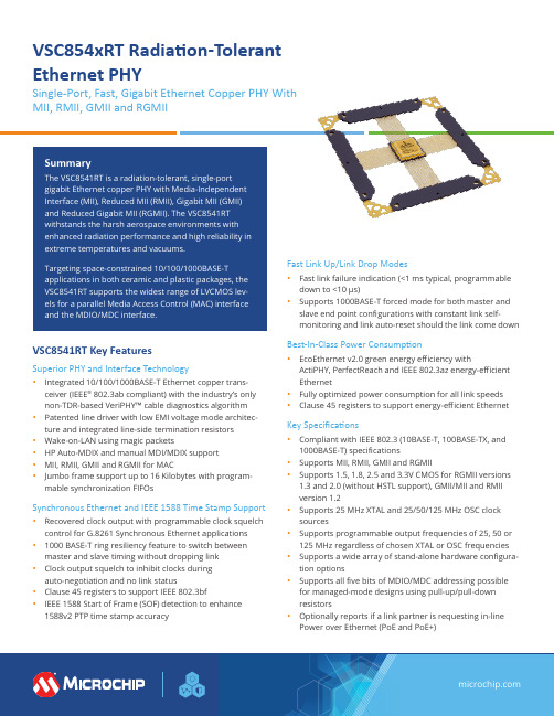
VSC854xRT Radiation-Tolerant Ethernet PHYSingle-Port, Fast, Gigabit Ethernet Copper PHY With MII, RMII, GMII and RGMIIVSC8541RT Key FeaturesSuperior PHY and Interface Technology• Integrated 10/100/1000BASE-T Ethernet copper trans-ceiver (IEEE ® 802.3ab compliant) with the industry’s only non-TDR-based VeriPHY™ cable diagnostics algorithm • Patented line driver with low EMI voltage mode architec-ture and integrated line-side termination resistors • Wake-on-LAN using magic packets• HP Auto-MDIX and manual MDI/MDIX support • MII, RMII, GMII and RGMII for MAC•Jumbo frame support up to 16 Kilobytes with program-mable synchronization FIFOsSynchronous Ethernet and IEEE 1588 Time Stamp Support • Recovered clock output with programmable clock squelch control for G.8261 Synchronous Ethernet applications • 1000 BASE-T ring resiliency feature to switch between master and slave timing without dropping link • Clock output squelch to inhibit clocks during auto-negotiation and no link status• Clause 45 registers to support IEEE 802.3bf•IEEE 1588 Start of Frame (SOF) detection to enhance1588v2 PTP time stamp accuracyFast Link Up/Link Drop Modes• Fast link failure indication (<1 ms typical, programmable down to <10 μs)•Supports 1000BASE-T forced mode for both master and slave end point configurations with constant link self-monitoring and link auto-reset should the link come downBest-In-Class Power Consumption• EcoEthernet v2.0 green energy efficiency with ActiPHY, PerfectReach and IEEE 802.3az energy-efficient Ethernet• Fully optimized power consumption for all link speeds •Clause 45 registers to support energy-efficient EthernetKey Specifications• Compliant with IEEE 802.3 (10BASE-T, 100BASE-TX, and 1000BASE-T) specifications• Supports MII, RMII, GMII and RGMII• Supports 1.5, 1.8, 2.5 and 3.3V CMOS for RGMII versions 1.3 and 2.0 (without HSTL support), GMII/MII and RMII version 1.2• Supports 25 MHz XTAL and 25/50/125 MHz OSC clock sources• Supports programmable output frequencies of 25, 50 or 125 MHz regardless of chosen XTAL or OSC frequencies • Supports a wide array of stand-alone hardware configura -tion options• Supports all five bits of MDIO/MDC addressing possible for managed-mode designs using pull-up/pull-down resistors•Optionally reports if a link partner is requesting in-line Power over Ethernet (PoE and PoE+)The Microchip name and logo and the Microchip logo are registered trademarks of Microchip Technology Incorporated in the U.S.A. and other countries. All other trademarks mentioned herein are property of their respective companies. © 2021, Microchip Technology Incorporated. All Rights Reserved. 7/21 DS00003337BSpace Environment• Full wafer lot traceability• 68-pin hermetic ceramic CQFP package • Space-grade screening and qualification• Total ionizing dose: up to 100 krad (Si), QML and ESCC)• Heavy ions and protons test• Single event latch-up LET > 78 MeV.cm²/mg •SEU full characterization for all functional blockHiRel/New Space Application• Full wafer lot traceability • 68-pin plastic VQFN package• QML-N/AQEC/AEC-Q100 equivalent• Unitary burn-in and temperature cycling (opt.)• Qual pack documentation •Single lot date codeVSC8540RTThe Radiation-Tolerant, Single-Port, Fast Ethernet Copper PHYTargeting space-constrained 10/100BASE-T applications in both ceramic and plastic packages, the VSC8540RT is a radiation-tolerant, single-port, fast Ethernet copper PHY with RGMII/MII/RMII interfaces that withstands the harsh aerospace environments with enhanced radiation performance and high reliability in extreme temperatures and vacuums. With its equivalent feature set, VSC8540RT is the radiation-tolerant Ethernet PHY solution for customers not requiring gigabit capabilities.VSC8541 Evaluation KitProduct Selection GuideTHERMDATHERMDCP0_D0N P0_D0P P0_D1N P0_D1P P0_D2N P0_D2P P0_D3N P0_D3PRCVRD_CLK CLK_SQUELCH_IN FASTLINK_FAILCLKOUTXTAL1/REFCLK XTAL2REFCLK_SEL[1:0]REF_FILT_A REF_REXT_ALED[1:0]。
ANALOG DEVICES ADSP-21535 说明书
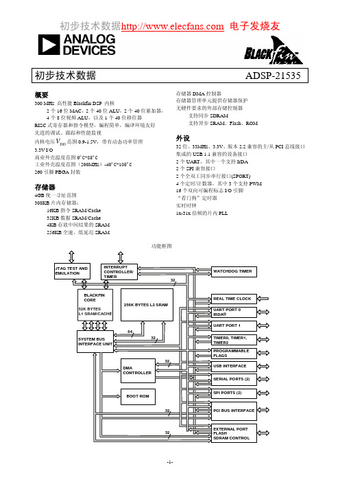
初步技术数据 电子发烧友概要300 MHz 高性能Blackfin DSP 内核2个16位MAC,2个40位ALU,2个40位累加器,4个8位视频ALU,以及1个40位移位器RISC式寄存器和指令模型,编程简单,编译环境友好先进的调试、跟踪和性能监视内核电压DDV范围0.9-1.5V,带有动态功率管理3.3V I/O商业外壳温度范围0ºC-85ºC工业外壳温度范围(200MHz)-40ºC-105ºC260引脚PBGA封装存储器4GB统一寻址范围308KB片内存储器:16KB指令SRAM/Cache32KB数据SRAM/Cache4KB存放中间结果的SRAM256KB全速、低延迟SRAM 存储器DMA控制器存储器管理单元提供存储器保护无硬件要求的外部存储控制器支持同步SDRAM支持异步SRAM、Flash、ROM外设32位、33MHz、3.3V、版本2.2兼容的主/从PCI总线接口集成的USB 1.1兼容的设备接口2个UART,其中一个支持IrDA2个SPI兼容接口2个全双工同步串行接口(SPORT)4个定时/计数器,其中3个支持PWM16个双向可编程标志I/O引脚“看门狗”定时器实时时钟1x-31x倍频的片内PLL初步技术数据ADSP-21535 2002年6月说明本数据手册提供的是关于ADSP-21535 Blackfin DSP 的初步信息。
概述ADSP-21535 是Blackfin DSP系列产品的成员之一,由AD公司和Intel公司共同开发,采用了Micro Signal Architecture (MSA)。
这种体系结构将艺术级的dual-MAC DSP引擎,简洁的RISC式微处理器指令集的优点,以及单指令多数据(SIMD)多媒体能力结合起来,形成了一套独特的指令集结构。
通过集成业界领先和丰富的系统外设及存储器,Blackfin DSP系列成为下一代需要将RISC式编程、多媒体支持和前沿的信号处理等集成在片内的DSP的选择平台。
Synopsys OptoDesigner 2020.09安装指南说明书
3. Troubleshooting scanning issues........................................................25
Accidental full scan proliferation by folder paths which include build or commit ID............................ 25 Solution......................................................................................................................................25
Contents
Contents
Preface....................................................................................................5
1. Scanning best practices......................................................................... 8
Clonezilla Basics for Windows Embedded说明书

Clonezilla Basics for Windows EmbeddedBy Sean D. Liming and John R. MalinAnnabooks –August 22, 2014Cloning a master image for mass production is an important step for Windows Embedded Standard and Windows Embedded Industry. First, the image must be rolled back to create the master, which is accomplished using sysprep. Here is an example command:Sysprep /generalize /oobe /shutdown /unattend:c:\myunattend.xmlThe unattended XML file is a small answer file that handles several of the Out-of-Box Experience (OOBE) screens as well as accounts, run–time key, computer names, etc. There are those that say you don’t need sysprep, but failure to run sysprep and just copy the image can run into technical consequences. In short, one must run sysprep to duplicate the image.Once the image has been rolled back, the next step is to capture the master image for deployment to other systems. The books: Starter Guide for Windows® System Image Manager, Professional's Guide To Windows® Embedded 8 Standard, and Professional's Guide To Windows® Embedded Standard 7 - 2nd Edition cover creating the unattended file and running sysprep, but what is not covered is an actual full disk capture utility. There are several hardware disk duplication solutions for hard drive and compact flash cards. International Microsystems I nc. and Logicube are two companies that offer hardware duplication products. . There are also software solutions, but some of the most popular like Norton Ghost are going end-of-life in favor of licensed server-based solutions. Microsoft has solutions to capture partitions into WIM files, but when multiple partitions need to be captured, the WIM file solution is very cumbersome. Simple and inexpensive software image capture solutions are becoming hard to find. Luckily, the Linux community has developed a solution called Clonezilla that captures full disk images; and best of all, it is a free solution that can be used to capture a Windows Embedded master image.This paper walks through the steps to create a Clonezilla disk to capture and deploy a Windows Embedded master disk image. You will need two USB flash disks. One will hold the Clonezilla boot disk image (USB disk size 8 GB), and the other will hold the captured image (USB flash disk size 32 GB or greater recommended).Note: This paper is based on Clonezilla 2.2.3-25 live image. The steps and pictures will be different for later versions.Generate Clonezilla boot diskWe start on the development machine, and download a utility to help create the Clonezilla boot disk.1. Download Tuxboot from . The actual download comes from SourceForge.2. Format the smaller USB flash disk as FAT 32. Format the larger flash disk as exFAT.3. Plug the smaller USB flash disk into the development machine and run Tuxboot.4. The Tuxboot application will start. Make sure that clonezilla_live_stable is selected forthe On-Line Distribution. Also, point to the correct USB flash drive.5. Click OK to start the process. The Clonezilla ISO will be downloaded, mounted locally,and then copied over to the flash disk.6. Do not reboot when asked. Just Exit Tuxboot.7. Safely eject the USB flash drive.Capture Disk ImageNow, we move to the target system that holds the master image.1. Plug the Clonezilla boot disk that we just created into the target system.2. Boot the target and make sure the BIOS is set up to boot from the USB flash disk.3. The Clonezilla boot screen appears. Select Clonezilla Live (Default settings, VGAXXXxYYY) and hit Enter.4. The OS will load. Select English as the language to use and hit Enter.5. Keep the default Don’t touch keymap and hit Enter.6. The default Start_Clonezilla Start Clonezilla should be selected, hit Enter.7. In the next menu, select device-image work with disks or partitions using images asthe operation mode and hit Enter.8. The next menu is for the image directory. Keep the default, local_dev, and hit Enter.9. Insert the larger USB flash disk when prompted, wait about 5 seconds, and then hitEnter.10. The system will mount and prepare the UBS flash disk for the image. You will be askedfor the home directory to store the image. Select the USB flash disk image (sdx1) and hit Enter.11. The top directory is the default, hit Enter.12. A summary will appear, hit Enter.13. The clone wizard starts. Select Beginner and hit Enter.14. The Select Mode screen appears. Select save disk, and hit Enter.15. An image name with date has been started. Rename the image as you like. For example“Annabooks-2014-08-18-19-img”, hit Enter.16. The hard disk will be selected as the default source. Hit Enter.17. Select Skip checking/repairing source file system, hit Enter.18. Check save disk image option appears, the default is Yes, check the saved image. HitEnter.19. Hit Enter to continue.20. Click y at the prompt and hit Enter to begin the backup process.21. The capture and check process takes several minutes depending on image size. HitEnter when completed22. Select Poweroff to Power down the system, and hit Enter.23. Remove both flash disks after the target powers down.Deploy the Captured Disk ImageThe two USB disks to capture the image can now be used to deploy the image to other systems.1. Plug the Clonezilla boot disk into the target system.2. Boot the target and make sure the BIOS is setup to boot from the USB flash disk.3. The Clonezilla boot screen appears. Select Clonezilla Live (Default settings, VGAXXXxYYY) and hit Enter.4. The OS will load. Select English as the language to use and hit Enter.5. Keep the default Don’t touch keymap and hit Enter.6. The default Start_Clonezilla Start Clonezilla should be selected, hit Enter.7. In the next menu, select device-image work with disks or partitions using images asthe operation mode and hit Enter8. The next menu is for the image directory. The default is for local_dev, hit Enter.9. Insert the larger USB flash disk when prompted, wait about 5 seconds, and then hitEnter.10. The system will mount and prepare the UBS flash disk for the image. You will be askedfor the home directory to store the image. Select the USB flash disk image (sdx1) and hit Enter.11. The top directory is the default, hit Enter.12. A summary will appear, hit Enter.13. The clone wizard starts. Select Beginner and hit Enter.14. The Select Mode screen appears. Select restoredisk and hit Enter.15. The system will search the disk for an image. Since there is only one image on the disk, itis already select, so hit Enter.16. Select the hard drive and hit Enter.17. Hit Enter again.19. One more time, enter y at the prompt and hit Enter.20. The process can take several minutes. Hit Enter when completed.21. Select to Poweroff to power down the system, and hit Enter.22. Remove both flash disks after the target powers down.23. Boot the system again and let the Windows cloning process run on the system.Once the master Clonezilla image has been created, it can be deployed any number of times to identical target hardware systems. This could easily be incorporated as part of the manufacturing process for an embedded system product.。
adi dsp内核资源
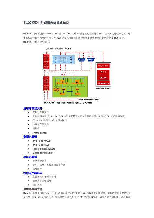
BLACKFIN 处理器内核基础知识Blackfin 处理器包括一个具有10 级RISC MCU/DSP 流水线的高性能16/32 位嵌入式处理器内核、用于实现最佳代码密度的可变长度ISA 以及具有面向加速视频和多媒体处理的指令的全SIMD 支持。
Blackfin 内核的说明如下:通用寄存器文件∙数据寄存器文件∙数据类型包括8 位、16 位或32 位带符号或无符号整数以及16 位或32 位带符号分数∙32 位读出和两个32 位写入操作∙地址寄存器文件∙栈指针∙Frame pointer数据运算器∙Two 16-bit MACs∙Two 40-bit ALUs∙Four 8-bit video ALUs∙Single barrel shifter地址运算器∙存储器取指令∙索引、长度、基数和修改寄存器∙循环缓冲程序定序器单元∙条件转移和子程序调用∙嵌套式零开销循环∙代码密度通用寄存器文件Blackfin 处理器内核包括一个用于通用运算单元的8 路×32 位数据寄存器文件。
支持的数据类型包括8 位、16 位或32 位带符号或无符号整数以及16 位或32 位带符号分数。
在每个时钟周期中,这种多端口寄存器文件均支持两个32 位读出和两个32 位写入操作。
还可将其作为一个16 路×16 位数据寄存器文件来进行存取。
除了支持循环缓冲和栈保持以外,地址寄存器文件还提供了一种通用型寻址机制。
该寄存器文件由8 个表目组成,并包括一个帧指针和一个栈指针。
帧指针可用于子例程参数传输,而栈指针则可用于存储子程序调用的返回地址。
数据运算器数据运算器所包含的系统资源大约是Analog Devices 公司以往16 位架构的两倍。
它包括:∙两个16 位MAC∙两个40 位ALU∙四个8 位视频ALU∙单个桶形移位器所有的计算资源均能够处理来自数据寄存器文件(R0~R7)的8 位、16 位或32 位操作数。
可将每个寄存器作为一个32 位寄存器或一个16 位寄存器的高位部分或低位部分来进行存取。
Blackfin CM-BF533 硬件用户手册说明书
Hardware User Manual CM-BF533 V2.0 (V1.3)ContactBluetechnix Mechatronische Systeme GmbHWaidhausenstr. 3/19A-1140 ViennaAUSTRIA/EUROPE*********************Document No.: 100-1203-2.0Version 6Date: 2007-04-05Table of Contents1Introduction (1)1.1Overview (1)1.2Benefits (2)1.3Applications (2)2Specification (3)2.1Functional Specification (3)2.2Boot Mode (3)2.3Memory Map (4)2.4Electrical Specification (4)2.4.1Supply Voltage (4)2.4.2Supply Voltage Ripple (4)2.4.3External Oscillator Frequency (4)2.4.4Real Time Clock Crystal (4)2.4.5Supply Current (4)2.5Environmental Specification (4)2.5.1Temperature (4)2.5.2Humidity (5)3CM-BF533 (Connector Version) (6)3.1Mechanical Outline (6)3.2Connector Footprint (7)3.3Top Mounted Connector (8)3.4Schematic Symbol (Signals of P1 and P2) (9)3.5Connectors Pin Assignment P1 – (1-60) (10)3.6Connector Pin Assignment P2 – (61-120) (11)3.7ITU656 Camera Connector P3 (1-22) (12)3.8Connector P4 (1-10) (12)4Test Points (13)4.1Footprint – Test Points (13)5Application Examples (14)5.1Sample Application (14)5.2Stand-alone Camera System (15)5.3Generic Signal Processing System (15)5.4Coprocessor Application (15)5.5Digital Video System (16)5.6Design Services (16)6Software Support (17)6.1BLACKSheep (17)6.2uClinux (17)7Known Bugs (18)8Product Changes (19)9Document Revision History (20)A List of Figures and Tables (21)Edition 2007-02© Bluetechnix Mechatronische Systeme GmbH 2007All Rights Reserved.The information herein is given to describe certain components and shall not be considered as a guarantee of characteristics.Terms of delivery and rights of technical change reserved.We hereby disclaim any warranties, including but not limited to warranties of non-infringement, regarding circuits, descriptions and charts stated herein.Bluetechnix makes and you receive no warranties or conditions, express, implied, statutory or in any communication with you. Bluetechnix specifically disclaims any implied warranty of merchantability or fitness for a particular purpose.Bluetechnix takes no liability for any damages and errors causing of the usage of this board. The user of this board is responsible by himself for the functionality of his application. He is allowed to use the board only if he has the qualification. More information is found in the General Terms and Conditions (AGB).InformationFor further information on technology, delivery terms and conditions and prices please contact Bluetechnix ().WarningsDue to technical requirements components may contain dangerous substances.BLACKFIN ProductsCore Modules:CM-BF533: Blackfin Processor Module powered by Analog Devices single coreADSP-BF533 processor; up to 600MHz, 32MB RAM, 2MB Flash,120 pin expansion connector and a size of 36.5x31.5mmCM-BF537E: Blackfin Processor Module powered by Analog Devices single coreADSP-BF537 processor; up to 600MHz, 32MB RAM, 4MB Flash,integrated TP10/100 Ethernet physical transceiver, 120 pin expansionconnector and a size of 36.5x31.5mmCM-BF537U: Blackfin Processor Module powered by Analog Devices single coreADSP-BF537 processor; up to 600MHz, 32MB RAM, 4MB Flash,integrated USB 2.0 Device, 120 pin expansion connector and a size of36.5x31.5mmTCM-BF537: Blackfin Processor Module powered by Analog Devices single coreADSP-BF537 processor; up to 500MHz, 32MB RAM, 8MB Flash,28x28mm, 120 pin expansion connector, Ball Grid Array or BorderPads for reflow soldering, industrial temperature range -40°C to+85°C.CM-BF561: Blackfin Processor Module powered by Analog Devices dual coreADSP-BF561 processor; up to 2x 600MHz, 64MB RAM, 8MBFlash, 120 pin expansion connector and a size of 36.5x31.5mmCM-BF527: From Q3 '07 a new Blackfin Processor Module powered by AnalogDevices single core ADSP-BF527 processor will be available; keyfeatures are USB OTG 2.0 and Ethernet. 2x120pin expansionconnectors are backwards compatible to other Core Modules.CM-BF548: From Q3 '07 a new Blackfin Processor Module powered by AnalogDevices single core ADSP-BF548 processor will be available; keyfeatures are 64MB DDR SD-RAM 2x100pin expansion connectors.Development Boards:EVAL-BF5xx: Low cost Blackfin processor Evaluation Board with one socket forany Bluetechnix Blackfin Core Module. Additional periphery isavailable, such as a SD-Card.DEV-BF5xxDA-Lite: Get ready to program and debug Bluetechnix Core Modules with thistiny development platform including a USB Based Debug Agent. TheDEV-BF5xxDA-Lite is a low cost starter development systemincluding VDSP++ Evaluation Software License.DEV-BF5xx-FPGA: Backfin Development Board with two sockets for any combination ofBlackfin Core Modules. Additional periphery is available, such asSD-Card, Ethernet, USB host, multi-port JTAG including a USBbased Debug Agent, connector for a LCD-TFT Display and connectorfor a digital camera system. A large on-board SPARTAN-3 FPGAand Soft IPs make this board the most flexible Blackfin developmentplatforms ever developed.Available Q2 2007EXT-Boards: The following Extender Boards are available: EXT-BF5xx-Audio,EXT-BF5xx-Video, EXT-BF5xx-Camera, EXT-BF5xx-Exp, *EXT-BF5xx-LVDS, *EXT-BF5xx-ETH-USB, *EXT-BF5xx-AD/DA.Additional boards based on customer request*Available Q2 2007Software Support:BLACKSheep: The BLACKSheep VDK is a multithreaded framework for theAnalog Devices Blackfin processor family that includes driversupport for a variety of hardware extensions. It is based on the real-time VDK kernel included within the VDSP++ developmentenvironment.LabVIEW: LabVIEW embedded support for the CM-BF537E, CM-BF537U andTCM-BF537 Core Modules based on the BLACKSheep VDK driverFramework.uClinux: All the Core Modules are supported by uClinux. The required bootloader and uClinux can be downloaded at .BLACKFIN Design ServiceBased on over three years Blackfin experience Bluetechnix offers development assistance as well as custom design services and software development.1 IntroductionThe CM-BF533 is a tiny, high performance and low power DSP/RISC core module incorporating Analog Devices Blackfin family of processors. The module allows easy integration into high demanding very space and power limited applications.1.1 OverviewThe Core Module CM-BF533 consists of the following components:Figure 1-1: Main Components of the CM-BF533 module▪Analog Devices Blackfin Processor BF533o ADSP-BF533SKBCZ600 (0°-70°C) Standard mounto ADSP-BF533SBBCZ500 (-40°-85°C) Option upon request▪32 MB SDRAMo SDRAM clock up to 133 MHzo MT48LC16M16A2BG-7 (16Mx16 at 3.3 V)▪2MB of Addressable Flasho ITLRC28F320J3C110 (2Mx16 at 3.3 V; 2MByte addressable only)o Additionally flash memory can be connected through the expansion board as parallel flash using asynchronous chip select lines or as a SPI flash.▪Low Voltage Reset Circuito Resets module if power supply goes below 2.93 V for at least 140 ms▪Dynamic Core Voltage Controlo Allows to adjust core voltage by setting software registers at the Blackfin Processoro Core voltage range: 0.8 – 1.32V▪Expansion Connector Ao Data Buso Address Buso Control Signalso Power Supply▪Expansion Connector Bo SPORT 0 and SPORT 1o JTAGo UARTo SPIo PPI (Parallel Port Interface)o GPIO’s1.2 Benefits▪The CM-BF533 is very compact and measures only 36.5x31.5mm▪Allows quick prototyping of product that comes very close to the final design ▪Reduces development costs, faster time to market▪Very cost effective for small and medium volumes1.3 Applications▪Generic high performance signal processor module▪Internet Connected Embedded System▪High performance web camera▪Robotics: Tiny processor module for mobile robots2 Specification2.1 Functional SpecificationFigure 2-1: Detailed Block DiagramFigure 2-1 shows a detailed block diagram of the CM-BF533 module. Beside the SDRAM control pins the CM-BF533 has all other pins of the Blackfin processor at its two main 60 pin connectors.Dynamic voltage control allows reducing power consumption to a minimum adjusting the core-voltage and the clock frequency dynamically in accordance to the required processing power.A low voltage reset circuit guarantees a power on reset and resets the system when the input voltage drops below 2.93V.2.2 Boot ModeDefault Boot Mode = 00 (BMODE1 = LOW, BMODE0 = LOW)BMODE0, BMODE1 has internal pull-down resistorConnect BMODE0 to Vcc and leave BMODE1 pin open for Boot Mode 01 (equals to 8 or 16 bit PROM/FLASH boot mode), this is the default boot mode of the Blacksheep software. See Blackfin Datasheets or Eval/DevBoard manuals for more details.2.3 Memory MapTable 2-1: Memory Map2.4 Electrical Specification2.4.1 Supply Voltage▪ 3.3 V DC +/-10%2.4.2 Supply Voltage Ripple▪100 mV peak to peak 0-20MHz2.4.3 External Oscillator Frequency▪25MHz2.4.4 Real Time Clock Crystal▪32.768kHz2.4.5 Supply Current▪Maximumsupplycurrent:**********▪Operating conditions:o Processor running at 600MHz, Core Voltage 1.2V, SDRAM 20% bandwidth utilization at 130MHz: 150mAo Processor running at 300MHz, Core Voltage 0.8V SDRAM 20% bandwidth utilization at 130MHz: 90mA2.5 Environmental Specification2.5.1 TemperatureDevelopment Version:▪Operating at full 600MHz: 0 to + 70° CIndustrial Version: (Only available upon request at a MOQ)2.5.2 HumidityOperating: 10% to 90% (non condensing)3 CM-BF533 (Connector Version)3.1 Mechanical OutlineTOP VIEWAll dimensions are given in millimeters!P336.517.57.059.2532.46.8526.7528.0531.522.450.60.35Ø0.652.551.7P1P27.759.0514.653452Figure 3-1: Mechanical outline and Bottom ConnectorsThe mechanical outline represents a top view of the connectors placed at the bottom of the core board.The module is shipped with two 60pin connectors.Figure 3-2: Side View with Connector mountedThe total minimum mounting height including receptacle at the motherboard is 6.1 mm.3.2 Connector FootprintIf the connector version (2x Hirose 0.6mm pitch) is used, the footprint for the baseboard may look as shown in Figure 3-3.For the baseboard the following connectors have to be used:Table 3-1: Baseboard connector typesThe connectors on the CM-BF533 are of the following type:Table 3-2: Module connector types36.526.7531.57.756.85Figure 3-3: Connector Footprint for Baseboard3.3 Top Mounted ConnectorThe optionally mounted connector P4 will not be supported in future versions.Figure 3-4: TOP VIEW3.4 Schematic Symbol (Signals of P1 and P2)SPORT0SPORT1PPIUARTSPIJTAGDataBusAddr.BusControlSignals Figure 3-5: Schematic Symbol of Module3.5 Connectors Pin Assignment P1 – (1-60)Table 3-3: Connector P1 pin assignmentAll Pin names of the connectors correspond to the names found in the Blackfin BF533 datasheet from Analog Devices.3.6 Connector Pin Assignment P2 – (61-120)Table 3-4: Connector P2 pin assignmentNon processor Pins:CLK_OUT: 25MHz buffered output clock of main oscillatorAll other pins are connected directly to the respective ADSP-BF533 processor pins.For details about the meaning of the signal names consult the Blackfin ADSP-BF533 datasheet.3.7 ITU656 Camera Connector P3 (1-22)The ITU656 connector has been tested only for the OmniVision cameras available in our camera kit Kit-CAM-OV. It is not recommended to use this connector!Table 3-5: Connector P3 pin assignment3.8 Connector P4 (1-10)The top optionally mounted connector P4 can be used as a stand-alone connector for a system requiring only power supply and one or two communication ports (UART and SPI)Table 3-6: Connector P4 pin assignment4 Test Points4.1 Footprint – Test Points9.859.251.25.057.4510.751.7524.0526.4529.7520.751233031322960596162909192119120Ø0.731.536.5Figure 4-1: Test Points of the Core Module5 Application Examples5.1 Sample ApplicationIn this minimum configuration the CM-BF533 is used as a high performance SPI-based co-processor module.Figure 5-1: Minimum Configuration with SPI and JTAG Connector5.2 Stand-alone Camera SystemThe CM-BF533 module can be used as a stand-alone module for a camera system requiring only power supply and the direct attachment of a compatible video camera. A camera kit including drivers can be purchased from Bluetechnix: KIT-CAM-OV (O.Nr 100-9901) The digital ITU656 camera directly connects to P3 while the power supply and any of two communication ports (SPI and UART) can be connected to the 10 pin P4 connector as well as over the large connectors P1 and P2 at the bottom.3.3 V Power, SPI, UARTFigure 5-2: Stand-alone Camera System5.3 Generic Signal Processing SystemFigure 5-3: Block Diagram – Analog Signal Processing Module5.4 Coprocessor ApplicationFigure 5-4: Block Diagram – Coprocessor Module5.5 Digital Video SystemFigure 5-5: Block Diagram: Digital Video System5.6 Design ServicesBluetechnix offers custom design services and software development.6 Software Support6.1 BLACKSheepThe Core Module is delivered with a pre-flashed basic version of the BLACKSheep VDK multithreaded framework. It contains a boot-loader for flashing the Core Module via the serial port.Please mind the software development documents.6.2 uClinuxThe Core Module is supported by the open source platform at . Since the Core Modules are pre-flashed with BLACKSheep you have to flash uBoot first. For flashing the uBoot you can use the BLACKSheep boot-loader.7 Known BugsTable 7-1: Known Bugs8 Product ChangesTable 8-1: Product Changes9 Document Revision HistoryTable 9-1: Revision HistoryA List of Figures and TablesFiguresFigure 1-1: Main Components of the CM-BF533 module (1)Figure 2-1: Detailed Block Diagram (3)Figure 3-1: Mechanical outline and Bottom Connectors (6)Figure 3-2: Side View with Connector mounted (6)Figure 3-3: Connector Footprint for Baseboard (7)Figure 3-4: TOP VIEW (8)Figure 3-5: Schematic Symbol of Module (9)Figure 4-1: Test Points of the Core Module (13)Figure 5-1: Minimum Configuration with SPI and JTAG Connector (14)Figure 5-2: Stand-alone Camera System (15)Figure 5-3: Block Diagram – Analog Signal Processing Module (15)Figure 5-4: Block Diagram – Coprocessor Module (15)Figure 5-5: Block Diagram: Digital Video System (16)TablesTable 2-1: Memory Map (4)Table 3-1: Baseboard connector types (7)Table 3-2: Module connector types (7)Table 3-3: Connector P1 pin assignment (10)Table 3-4: Connector P2 pin assignment (11)Table 3-5: Connector P3 pin assignment (12)Table 3-6: Connector P4 pin assignment (12)Table 7-1: Known Bugs (18)Table 8-1: Product Changes (19)Table 9-1: Revision History (20)。
Blackfin LDF文件格式详解

Blackfin LDF文件格式详解对ADSP-BF533 Blackfin处理器,VisualDSP++提供4个.LDF文件:如果.LDF文件名没有后缀,那它就是“缺省的.LDF文件”。
即,如果没有明确指定某个.LDF文件,编译器连接应用程序时会使用缺省的.LDF文件。
例如,ADSP-BF531.ldf是ADSP-BF531 Blackfin处理器的缺省的.LDF文件。
对每个处理器,有三个.LDF文件,后缀是_C、_CPP和_ASM (例如ADSP-BF533_C.ldf)。
这些.LDF文件是Expert Linker的模板。
Blackfin处理器的.LDF文件可以分为5个主要部分:•前导段•库选择•run-time头选择•存储空间声明•代码/数据到存储器映射定义每个.LDF文件处理一系列命令,允许通过提供少量命令行选项来把多种配置植入应用。
通过在.LDF文件中大量使用预处理器宏,******************************************************************************* **//ARCHITECTURE指令规定这个.LDF文件用于ADSP-BF533 Blackfin处理器。
ARCHITECTURE(ADSP-BF533)******************************************************************************* **SEARCH_DIR指令识别标准run-time库的位置,像VisualDSP++安装目录的Blackfin\lib子目录一样。
链接器将$ADI_DSP置为VisualDSP++安装目录。
如果选择__NO_STD_LIB选项,不包括SEARCH_DIR指令,这意味着链接器没有搜索run-time库的缺省空间。
这个选项由-no-std-lib编译器开关选择,确保应用仅被用户提供的库链接。
ANSI-TIA-EIA-568-B.2-1 Cat.6 June 20 2002

PUBLICATIONS or call Global Engineering Documents, USA and Canada (1-800-854-7179) International (303-397-7956)
All rights reserved Printed in U.S.A.
PLEASE! DON'T VIOLATE
This Standard does not purport to address all safety problems associated with its use or all applicable regulatory requirements. It is the responsibility of the user of this Standard to establish appropriate safety and health practices and to determine the applicability of regulatory limitations before its use.
Published by
最全DD-WRT 支持无线路由器列表
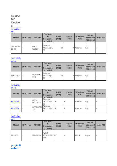
Suppor ted Device s[edit]3c[edit]Ab [edit]Ac [edit]Ac [edit ]Actiontec[edit ]ADIEnginee [edit ]Airl[edit ]Airlive /[edit ]AlfaNetwor[edit ]Alln[edit]Ana ptyx Wireles sDynami[edit]Ara da System[edit]As[edit]Asu sWARNIN G: It is recomme nded to use ASUS Firmware restorati on tool for ASUS routers initial flash (use*.TRX file)[edit ]BelkinWARNING:Always use TFTP to flash Belkin routers if at allpossible!Upgradin g dd-wrt from the webinterface can lead to abricked (nonfunc tional)unit![edit]Bou[edit]Bro[edit]Buf[edit]Cisc o [edit]Cisc oLinksys[edit]Cisc o Linksys[edit]Cisc o Linksys (Wireles s[edit ]Cisc[edit ]Conceptron [edit ]Compex[edit]Co nrad Elektron[edit]Co[edit ]Dev[edit ]Digi[edit ]D-Link[edit]Do odle[edit]Dy[edit]Edi[edit]En [edit ]EnGeniusseeSenao[edit ]ExelNetwor[edit]Flui[edit]FO[edit]Fr y's Electron ics[edit]Ga[edit]Gat[edit]In tellinet (Reichel t)see RFNet Techn ologi es[edit ]Io[edit ]JJPl[edit ]Lanready[edit]Lin ksysseeCisco[edit ]Log[edit ]Ma[edit ]Mer[edit]Mi MN-700@125[edit ]Mikrotik Routerb[edit]Mi [edit]Mo[edit]MS[edit]MT N Electron[edit]Ne[edit]Net[edit]NET[edit]Net[edit]No[edit]Op enMesh[edit]Ope[edit]OS[edit ]Ovislinksee Airli ve[edit ]PC-[edit ]Planex aka[edit]Ra[edit ]Ray[edit ]Rep[edit ]RFNetTechnol[edit]Ro[edit ]Senao / EnGeni。
FPGA可编程逻辑器件芯片EP1C12F324I7中文规格书

General-Purpose TimersOutput Pad DisableThe output pin can be disabled in PWM_OUT mode by setting the OUT_DIS bit in the TIMERx_CONFIG register. The TMRx pin is then three-statedregardless of the setting of PULSE_HI and TOGGLE_HI. This can reducepower consumption when the output signal is not being used. The TMRx pin can also be disabled by the PORTx_FER and the PORTx_MUX registers. Single Pulse GenerationIf the PERIOD_CNT bit is cleared, the PWM_OUT mode generates a single pulse on the TMRx pin. This mode can also be used to implement a precise delay.The pulse width is defined by the TIMERx_WIDTH register, and theTIMERx_PERIOD register is not used. See Figure10-5.At the end of the pulse, the timer interrupt latch bit TIMILx is set, and the timer is stopped automatically. No writes to the TIMER_DISABLEx register are required in this mode. If the PULSE_HI bit is set, an active high pulse is generated on the TMRx pin. If the PULSE_HI bit is not set, the pulse is active low.Figure 10-5. Timer Enable and Automatic Disable TimingADSP-BF54x Blackfin Processor Hardware Reference25UART PORT CONTROLLERS This chapter describes the universal asynchronous receiver/transmitter(UART) modules and includes the following sections:•“Overview” on page25-1•“Interface Overview” on page25-3•“Description of Operation” on page25-6•“Programming Model” on page25-22•“UART Registers” on page25-26•“Programming Examples” on page25-51OverviewThe ADSP-BF54x processor Blackfin processors feature multiple separate and identical UART modules.ADSP-BF548 and ADSP-BF549 processors feature four UARTs, referred to as UART0, UART1, UART2, and UART3. UART2 is not present on ADSP-BF542 and ADSP-BF544 devices.The UART modules are full-duplex peripherals compatible with PC-style industry-standard UARTs, sometimes called Serial Controller Interfaces (SCI). The UARTs convert data between serial and parallel formats. The serial communication follows an asynchronous protocol that supports var-ious word length, stop bits, bit rate, and parity generation options. ADSP-BF54x Blackfin Processor Hardware Reference。
PowerUp SYBR Green Master Mix说明书

PowerUp™ SYBR™ Green Master MixUniversal 2X master mix for real-time PCR workflowsCatalog Numbers A25741, A25742, A25743, A25776, A25777, A25778, A25779, A25780, A25918Pub. No. MAN0028468 Rev. B.0Note: For safety and biohazard guidelines, see the “Safety” appendix in the following product documentation: PowerUp™ SYBR™ Green Master Mix User Guide (Pub. No. MAN0013511). Read the Safety Data Sheets (SDSs) and follow the handling instructions. Wear appropriate protective eyewear, clothing, and gloves.This Quick Reference is intended as a benchtop reference for experienced users of PowerUp™ SYBR™ Green Master Mix. Fordetailed instructions, supplemental procedures, and troubleshooting, see the PowerUp™ SYBR™ Green Master Mix User Guide (Pub. No. MAN0013511).GuidelinesInput DNA template requirementsUse 1–10 ng single-stranded cDNA or 10–100 ng gDNA per reaction.IMPORTANT! In some cases, cDNA generated with the SuperScript™ IV VILO™ Master Mix is not compatible with the PowerUp™ SYBR™ Green Master Mix. It can result in a high background signal. To ensure consistent results across different samples and assays, we recommend a different reverse transcription kit.For kits recommended for reverse transcription of RNA to cDNA, see PowerUp™ SYBR™ Green Master Mix User Guide (Pub.No. MAN0013511).If you use SuperScript™ IV VILO™ Master Mix and your results do not show a high background signal with your assay and sample, you can continue to use the SuperScript™ IV VILO™ Master Mix and the PowerUp™ SYBR™ Green Master Mix.PCR reactions•Four replicates of each reaction are recommended.•Reaction mixes can be prepared depending upon experimental requirements. Scale the components according to the number of reactions and include 10% overage.•If using smaller reaction volumes, scale all components proportionally. Reaction volumes <10 µL are not recommended.NTC controlsNo template control (NTC) reactions can be used to identify PCR contamination. NTC reactions contain all reaction components (PowerUp™ SYBR™ Green Master Mix, primers, water) except sample, and therefore should not return a C t value.MethodsSet up the PCR reactions1.Prepare the appropriate number of reactions, plus 10% overage.[1]For optimal performance in Fast and Standard modes, use 300–800 nM for each primer.[2]Use 1–10 ng cDNA or 10–100 ng gDNA for each reaction.For Research Use Only. Not for use in diagnostic procedures.2.Mix the components thoroughly, then centrifuge briefly to spin down the contents and eliminate any air bubbles.3.Transfer the appropriate volume of each reaction to each well of an optical plate.4.Seal the plate with an optical adhesive cover, then centrifuge briefly to spin down the contents and eliminate any air bubbles.PCR can be performed on the reaction plate up to 24 hours after completing the set-up, when stored at room temperature.Set up and run the real-time PCR instrument1.Place the reaction plate in the real-time PCR instrument.2.Set the thermal cycling conditions using the default PCR thermal cycling conditions specified in the following tables according to theinstrument cycling parameters and melting temperatures of the specific primers.Note: Standard cycling conditions are recommended for genomic DNA templates. Use only standard cycling conditions for the 7900HT Real-Time PCR Instrument and the 7500 Real‑Time PCR Instrument.Table 1 Fast cycling mode (primer T m ≥60°C)[1]When using a QuantStudio™ Real-Time PCR System or a ViiA™ 7 Real-Time PCR System.[2]When using a 7500 Fast Real-Time PCR System, 7900HT Fast Real-Time PCR Instrument, StepOnePlus™ Real-Time PCR System, or StepOne™ Real-Time PCR System.Table 2 Standard cycling mode (primer T m ≥60°C)Table 3 Standard cycling mode (primer T m <60°C)[1]Anneal temperature should be set to the melting point for your primers.3.Set the instrument to perform a default dissociation step.A dissociation step can be performed up to 72 hours after the real-time PCR run if the plate is stored in the dark and up to 24 hoursafter the real-time PCR run if the plate is exposed to light.Table 4 Dissociation curve conditions (melt curve stage)[1]Dissociation2PowerUp™ SYBR™ Green Master Mix Quick ReferenceUse the following settings for Applied Biosystems™ instruments:•Experiment type: Standard curve•Reagent: SYBR™ Green reagents•Reporter: SYBR™•Quencher: None•Passive reference dye: ROX™•Ramp speed: Standard or fast (choose the same setting as in step 2)•Melt curve ramp increment: Continuous4.Set the reaction volume appropriate for the type of plate being used for your PCR reaction.5.Start the run.Analyze results1.View the amplification plots.2.Calculate the baseline and threshold cycles (C t) for the amplification curves using the instrument software.3.Check for nonspecific amplification using dissociation curves.4.Perform relative or absolute quantitation.Thermo Fisher Scientific Baltics UAB | V.A. Graiciuno 8, LT-02241 | Vilnius, LithuaniaFor descriptions of symbols on product labels or product documents, go to /symbols-definition.Revision history: Pub. No. MAN0028468The information in this guide is subject to change without notice.DISCLAIMER: TO THE EXTENT ALLOWED BY LAW, THERMO FISHER SCIENTIFIC INC. AND/OR ITS AFFILIATE(S) WILL NOT BE LIABLE FOR SPECIAL, INCIDENTAL, INDIRECT, PUNITIVE, MULTIPLE, OR CONSEQUENTIAL DAMAGES IN CONNECTION WITH OR ARISING FROM THIS DOCUMENT, INCLUDING YOUR USE OF IT.Important Licensing Information: This product may be covered by one or more Limited Use Label Licenses. By use of this product, you accept the terms and conditions of all applicable Limited Use Label Licenses.©2023 Thermo Fisher Scientific Inc. All rights reserved. All trademarks are the property of Thermo Fisher Scientific and its subsidiaries unless otherwise specified./support | /askaquestion19 January 2023。
Blackfin 专用管脚复用插件

Engineer-to-Engineer Note EE-341更多关于ADI公司的DSP、处理器以及开发工具的技术资料,请访问网站:/ee-note 和/processor如需技术支持,请发邮件至processor.support@或processor.tools.support@Blackfin®专用管脚复用插件作者:Jagadeesh Rayala Rev 1-May 15,2008 简介本文介绍了如何使用VisualDSP++®开发工具(5.0或更高版本的专用管脚复用插件来配置ADSP-BF54x和ADSP-BF52x的端口寄存器。
使用管脚复用插件可以自动生成C或汇编代码来配置端口寄存器,这样可以大大降低工作量。
管脚复用ADSP-BF52x和ADSP-BF54x系列Blackfin处理器具有一系列丰富的外设,通过强大的管脚复用机制,为外部应用空间提供很高的灵活性。
因为具有一系列丰富的外设端口,ADSP-BF52x处理器将这些外设信号分成四个端口组,分别为PORT F,PORT G,PORT H,PORT J。
对于ADSP-BF54x 来说,外设信号被分成了十个端口组,从PORT A到PORT J。
大多数相关管脚可以被多路信号来共享。
通过多路复用器控制端口的功能。
PORT A到PORT J的每个管脚(ADSP-BF52x处理器的PORT F,PORT G,PORT H)还能作为通用的输入输出管脚。
任何没有被外设功能占用的管脚都可以单独地被配置成GPIO模式。
在默认的情况下,重启以后的所有管脚都是GPIO模式。
但是GPIO的输入输出驱动在默认设置中都是未激活的。
每个端口都有一套自己的映射到内存的寄存器,用于控制端口复用和GPIO功能。
使用外设功能需要明确的使能寄存器(PORTx_FER,对于ADSP-BF52x此处x表示F,G,H)。
端口里面外设间的复用由另一个多路控制寄存器来控制(PORTx_MUX)。
balluff bni iol-709-000-k006 bni iol-710-000-k006

BNI IOL-709-000-K006 BNI IOL-710-000-K006IO-Link Sensor-Hub analogUser’s GuideContent1Notes to the user 21.1Structure of the guide 21.2Typographical conventions 2Enumerations 2 Actions 2 Syntax 2 Cross-references 21.3Symbols 21.4Abbreviations 21.5Divergent views 2 2Safety 32.1Intended use 32.2Installation and startup 32.3General safety Notes 32.4Resistance to Aggressive Substances 3Hazardous voltage 3 3Getting Started 43.1Connection overview 43.2Mechanical connection 53.3Electrical connection 53.4Function ground 53.5IO-Link connection 53.6Digital Sensors 63.7Analogue Sensors 6 4IO-Link Interface 74.1IO-Link Data 74.2Process data inputs 74.3Process data outputs 84.4Parameter data/ On-request data 8Identification data 8 Inversion 9 Switch point enable 9 Switch point 94.5Errors 104.6Events 10 5Technical Data 115.1Dimensions 115.2Mechanical data 115.3Electrical data 115.4Operating conditions 115.5Function indicators 12Module LEDs 12 Digital Input LEDs 12 Analogue Input LEDs 12 6Appendix 136.1Type designation code 136.2Order information 13IO-Link Sensor-HubBNI IOL-709-… / BNI IOL-710-…1 Notes to the user1.1 Structure of theguide The Guide is organized so that the sections build on one another. Section 2 : Basic safety information. …………1.2 Typographicalconventions The following typographical conventions are used in this Guide. EnumerationsEnumerations are shown in list form with bullet points.• Entry 1, • Entry 2.Actions Action instructions are indicated by a preceding triangle. The result of an action is indicated by an arrow.Action instruction 1. Action result.Action instruction 2. SyntaxNumbers:Decimal numbers are shown without additional indicators (e.g. 123),Hexadecimal numbers are shown with the additional indicator hex (e.g. 00hex ).Cross-references Cross-references indicate where additional information on the topic can be found.1.3 SymbolsAttention!This symbol indicates a security notice which most be observed.NoteThis symbol indicates general notes.1.4 AbbreviationsBCD BNI CV DPP I-Port EMC FE IOL LSB MSB SP SPDU VVBinary coded switch Balluff Network InterfaceCurrent Version: BNI IOL 709… Direct Parameter Page Digital input portElectromagnetic Compatibility Function ground IO-LinkLeast Significant Bit Most Significant Bit Switch PointService Protocol Data UnitVoltage version: BNI IOL 710…1.5 Divergent views Product views and images can differ from the specified product in this manual. They serve only as an illustration.2 Safety2.1 Intended use The BNI IOL-… is a decentralized sensor input module which is connected to a host IO-Linkmaster over an IO-Link interface.2.2 Installation andstartup Attention!Installation and startup are to be performed by trained technical personnel only. Skilled specialists are people who are familiar with the work such as installation and the operation of the product and have the necessary qualifications for these tasks. Any damage resulting from unauthorized tampering or improper use shall void warranty and liability claims against the manufacturer. The operator is responsible for ensuring that the valid safety and accident prevention regulations are observed in specific individual cases.2.3 General safetyNotes Commissioning and inspectionBefore commissioning, carefully read the User's Guide.The system must not be used in applications in which the safety of persons depends on the function of the device.Intended useWarranty and liability claims against the manufacturer shall be rendered void by damage from:•Unauthorized tampering•Improper use•Use, installation or handling contrary to the instructions provided in this User's Guide.Obligations of the owner/operator!The device is a piece of equipment in accordance with EMC Class A. This device can produce RF noise. The owner/operator must take appropriate precautionary measures against this for its use. The device may be used only with a power supply approved for this. Only approved cables may be connected.MalfunctionsIn the event of defects and device malfunctions that cannot be rectified, the device must be taken out of operation and protected against unauthorized use.Approved use is ensured only when the housing is fully installed.2.4 Resistance toAggressiveSubstances Attention!The BNI modules always have good chemical and oil resistance. When used in aggressive media (such as chemicals, oils, lubricants and coolants, each in a high concentration (i.e. too little water content)), the material must first be checked for resistance in the particular application. No defect claims may be asserted in the event of a failure or damage to the BNI modules caused by such aggressive media..Hazardous voltage Attention!Disconnect all power before servicing equipment.NoteIn the interest of continuous improvement of the product,Balluff GmbH reserves the right to change the technical data of the product and the content of these instructions at any time without notice.IO-Link Sensor-HubBNI IOL-709-… / BNI IOL-710-…3 Getting Started3.1 Connectionoverview1 Mounting hole2 IO-Link interface3 Analogue input-Port 14 Status-LED: Analogue port5 Analogue input port 36 Status-LED: digital input Pin 27 Digital input port 18 Status-LED: Digital port Pin 49 Digital input port 3 10 Status LED “Power Supply”11 Digital input port 212 Digital input port 013 Analogue input port 214 Analogue input port 015 Label16 Status-LED …COM“17 Function ground connection3 Getting Started3.2 Mechanicalconnection The BNI IOL modules are attached using 3 M4 screws (Item 1, Fig. 3-1/3-2).3.3 Electricalconnection The Sensor Hub modules require no separate supply voltage connection. Power is provided through the IO-Link interface by the host IO-Link Master.3.4 Function groundThe modules are provided with a ground terminal.Connect Sensor Hub module to the ground terminal.NoteThe FE connection from the housing to the machine must be low-impedance and as short as possible.3.5 IO-LinkconnectionThe IO-Link connection is made using an M12 connector (A-coded, male).IO-Link (M12, A-coded, male)Pin Function 1Supply voltage, +24 V, max. 1.6 A 2 - 3 GND, reference potential4 C/Q, IO-Link data transmission channelConnection protection ground to FE terminal, if present. Connect the incoming IO-Link line to the Sensor Hub.NoteA standard sensor cable is used for connecting to the host IO-Link Master.IO-Link Sensor-HubBNI IOL-709-… / BNI IOL-710-…3 Getting Started3.6 Digital Sensors Digital input port (M12, A-coded, female)Pin Function 1 +24 V, 100 mA 2 Standard Input 3 0 V, GND 4 Standard Input 5 -NoteFor the digital sensor inputs follow the input guideline per EN 61131-2, Type 2.3.7 AnalogueSensors Analogue input port (M12, A-coded, female)Pin Function1 +24 V, 100 mA2BNI IOL-709...: 4 - 20 mABNI IOL-710…:n.c. 3 0 V, GND4BNI IOL-710...: 0 - 10 V BNI IOL-709…:n.c 5 FE, function groundNoteUnused I/O port sockets must be fitted with cover caps to ensure IP67 protection rating.NoteOvercurrent (> 25mA) on the BNI IOL-709 Module´s inputs can distort the measurement results of the other channels and it may leads to malfunction..4 IO-Link Interface4.1 IO-Link Data Baudrate COM2 (38,4 kBaud)Frame type 1Minimum cycle time 3 msProcess data cycle 30 ms with minimum cycle time4.2 Process datainputs BNI IOL-710-…/BNI IOL-709-…(Sensor-Hub digital/analog)Process data length 10Byte:Byte 0 Byte 17 6 5 4 3 2 1 0 7 6 5 4 3 2 1 0InputPort7Pin4InputPort6Pin4InputPort5Pin4InputPort4Pin4SwitchPoint1Port3SwitchPoint1Port2SwitchPoint1Port1SwitchPoint1PortInputPort7.Pin2InputPort6.Pin2InputPort5.Pin2InputPort4.Pin2SwitchPoint2Port3SwitchPoint2Port2SwitchPoint2Port1SwitchPoint2PortByte 2 Byte 37 6 5 4 3 2 1 0 7 6 5 4 3 2 1 0Error1Error2Error3MSBAnalogue valueLSBPort 0Byte 4 Byte 57 6 5 4 3 2 1 0 7 6 5 4 3 2 1 0Error1Error2Error3MSBAnalogue valueLSBPort 1Byte 6 Byte 77 6 5 4 3 2 1 0 7 6 5 4 3 2 1 0Error1Error2Error3MSBAnalogue valueLSBPort 2Byte 8 Byte 97 6 5 4 3 2 1 0 7 6 5 4 3 2 1 0Error1Error2Error3MSBAnalogue valueLSBPort 3IO-Link Sensor-HubBNI IOL-709-… / BNI IOL-710-…4 IO-Link InterfaceInput: Input-Signal at Port and PinSwitch Point: The switch point bits show a switch pointoverrun. The switch point can be configuredby parameter ( see 0.0 - “Switch pointenable” and 0.0 - “Switch point”)Analogue value: VV: actual voltage value between0 and 1056 (1Bit = 0.01V)CV: actual current value between0 and 2150 (1Bit = 0.01mA)Error:• Error 1 • Error 2 • Error 3 Overcurrent/short circuit on sensor supply Measurement range overflow Measurement range undercut (only CV)4.3 Process dataoutputsThere are no outputs at BNI IOL-710-... and BNI IOL-709-... modules.4.4 Parameter data/On-request dataDPP SPDU Parameter DatawidthAccess Index Index Sub-indexIdentificationData07hex Vendor ID 2 ByteReadonly 08hex09hex Device ID 3 Byte0A hex0B hex10hex0 Vendor Name 8 Byte11hex0 Vendor text 16 Byte12hex0 Product Name 34 Byte13hex0 Product ID 21 Byte14hex0 Product text 34 Byte16hex Hardware Revision 3 Byte17hex0 Firmware Revision 3 ByteIdentification data Type Device ID VersionBNI IOL-710-000-K006 050201hex Voltage versionBNI IOL-709-000-K006 050202hex Current version4 IO-Link InterfaceDPPSPDUParameter Data width Value rangeDefault- valueIndex Index Sub-index P a r a m e t e r D a t a10hex 40hex640 1-16 Inversion 2 Byte 0000hex …FFFF hex 0000hex 11hex 12hex 41hex650 1-8 Switch point enable 1 Byte 00hex …FF hex 00hex 42hex660 Switch point 1 Port 0 2 Byte 0000hex … 03E8hex 0000hex 43hex670 Switch point 1 Port 1 2 Byte 0000hex … 03E8hex 0000hex 44hex680 Switch point 1 Port 2 2 Byte 0000hex … 03E8hex 0000hex 45hex690 Switch point 1 Port 3 2 Byte 0000hex … 03E8hex 0000hex 46hex700 Switch point 2 Port 0 2 Byte 0000hex … 03E8hex 0000hex 47hex710 Switch point 2 Port 1 2 Byte 0000hex … 03E8hex 0000hex 48hex720 Switch point 2 Port 2 2 Byte 0000hex … 03E8hex 0000hex 49hex73Switch point 2 Port 32 Byte0000hex … 03E8hex0000hexInversionInversion of the input signals:Byte 0Byte 176543217654321I n v e r s i o n P o r t 7 P i n 4I n v e r s i o n P o r t 6 P i n 4I n v e r s i o n P o r t 5 P i n 4I n v e r s i o n P o r t 4 P i n 4I n v e r s i o n S P 1 P o r t 3I n v e r s i o n S P 1 P o r t 2I n v e r s i o n S P 1 P o r t 1I n v e r s i o n S P 1 P o r t 0I n v e r s i o n P o r t 7 P i n 2I n v e r s i o n P o r t 6 P i n 2I n v e r s i o n P o r t 5 P i n 2I n v e r s i o n P o r t 4 P i n 2I n v e r s i o n S P 2 P o r t 3I n v e r s i o n S P 2 P o r t 2I n v e r s i o n S P 2 P o r t 1I n v e r s i o n S P 2 P o r t 0Switch point enableEnable the switch points by setting the enable bitsByte 07654321E n a b l e s w i t c h p o i n t 2 P o r t 3E n a b l e s w i t c h p o i n t 2 P o r t 2E n a b l e s w i t c h p o i n t 2 P o r t 1E n a b l e s w i t c h p o i n t 2 P o r t 0E n a b l e s w i t c h p o i n t 1 P o r t 3E n a b l e s w i t c h p o i n t 1 P o r t 2E n a b l e s w i t c h p o i n t 1 P o r t 1E n a b l e s w i t c h p o i n t 1 P o r t 0Switch pointByte 0Byte 1 7 6 5 4 3217654321Switch pointValue range (dec) CV= 400...2000 VV= 0 (1000)BNI IOL-709-… / BNI IOL-710-…4 IO-Link Interface4.5 Errors Byte 0Byte 1Device application error: 80hex11hex Index not available 12hex Subindex not available 30hex Value out of range4.6 EventsClass/QualifierCode (high + low)Mode Type InstanceP a r a m e t e r D a t aappears Error AL Device Hardware supply Supply low voltage U2 = supply + 24VC0hex 30hex 03hex 5000hex 0100hex 0010hex 0002hex F3hex5112hex disappears ErrorAL Device Hardware supply Supply low voltage U2 = supply + 24V80hex 30hex 03hex 5000hex 0100hex 0010hex 0002hexB3hex 5112hexappears Error AL Device Hardware supply supply peripheryC0hex30hex 03hex 5000hex 0100hex0060hexF3hex 5160hexdisappears ErrorAL Device Hardware supply supply periphery80hex30hex 03hex5000hex0100hex0060hexB3hex5160hex5 Technical Data5.1 Dimensions5.2 Mechanical data Housing Material Plastic, transparentIO-Link-Port M12, A-coded, maleInput-Ports 8x M12, A-coded, femaleEnclosure rating IP67 (only when plugged-in and threaded-in)Weight 90 gDimensions(L × W × H, excluding connector)115 × 50 × 30,8 mm5.3 Electrical data Operating voltage 18 ... 30,2 V DC, per EN 61131-2Ripple < 1 %Current draw without load ≤ 40 mA5.4 Operatingconditions Operating temperature -5 °C … +55 °C Storage temperature -25 °C … +70 °CBNI IOL-709-… / BNI IOL-710-…5 Technical Data5.5 FunctionindicatorsModule LEDs LED 5, IO-Link CommunicationStatus FunctionGreen No CommunicationGreen negative pulsed Communication OKRed Communication line overloadOff Module unpoweredLED 4, Power supply statusStatus FunctionGreen Module power is OKGreen slowly flashing Short circuitGreen rapidly flashing Module power supply < 18 VOff Module unpowered Digital Input LEDs LED 3, Input Pin 4 and LED 2, Input Pin 2Status FunctionYellow Input signal = 1Off Input signal = 0Analogue Input LEDs LED 1, Analogue input portStatus Signal 709 (4-20 mA) Signal 710 (0-10 V) Green ≥ 4 mA - ≤ 20 mA> 0,05 VRed < 4 mA - > 20 mA > 10,05 V6 Appendix6.1 Type designationcode6.2 OrderinformationType Order CodeBNI IOL-709-000-K006 BNI0007BNI IOL-710-000-K006 BNI0008BNI IOL-7xx-000-K006 Balluff Network InterfaceIO-Link interfaceFunctions710 = 8 digital inputs 0,15 A + 4 analog inputs 0 - 10 V709 = 8 digital inputs 0,15 A + 4 analog inputs 4 - 20 mAVariant000 = StandardvarianteMechanical configurationK006 =Plastic housing,Connectors:- BUS and Power supply: 1x M12x1, external thread- Input ports: 8x M12x1, internal threadBNI IOL-709-… / BNI IOL-710-… NotesBalluff GmbHSchurwaldstrasse 973765 Neuhausen a.d.F. GermanyTel. +49 7158 173-0 N r . 910442-726 E •01.125277 • E d i t i o n K 17 • R e p l a c e s E d i t i o n 1311 • S u b j e c t t o m o d i f i c a t i o n。
ADSP基础入门 第6讲 Blackfin嵌入式C编程

6
成信院-ADI联合实验室
Volatile的用法
volatile在英文字典的解释为“易变的,反复无常 的(性格)”。
编译器有一种技术叫数据流分析,分析程序中的变 量在哪里赋值、哪里使用、哪里失效,分析结果可 以用于常量合并,常量传播等优化。当它觉察到你 的代码没有修改变量的值时,它就可能在你访问变 量时提供上次访问的缓冲值,这能够提高程序的效 率。
编译器内置函数(Compiler Builtin Function),主要针对一些常 用的操作,其实现大多与处理器硬件电路有关。
内置函数一般采用汇编语言编写,一旦用户调用此函数,编译器直 接映射到相应的汇编代码中(会被编译器识别出来,使用固定的汇 编语句来代替库函数的调用),运行效率很高。
有一些内置函数是系统管理函数,这些内置函数将系统管理的各项 操作封装成函数,直接调用这些内置函数将能提高代码的可读性。
多任务环境中各任务间共享的标志应该加 volatile。
8
成信院-ADI联合实验室
C/C++编译语言扩展
编译器支持对ISO/ANSI 标准的C语言和C++语言 的扩展。 为了使C/C++扩展中附加关键字与ISO/ANSI 标准 C/C++的关键字不冲突, C/C++扩展中附加关键字 在形式上均以双下划线“__”打头。 标准C/C++关键字用一个下划线“_”打头,编译 器扩展C/C++关键字用两个下划线“__” 打头; 标准库函数名用一个下划线“_”打头,编译器扩 展的库函数(由编译器给出的内嵌函数)名用两 个下划线“__” 打头。
Spyder 4 科学型 Python IDE 用户指南说明书

Spyder 4 ... the python IDE for sciencePost 2020-05-24 by Dan Patterson (retired) Original Post by Dan Patterson 12-Dec-2019SpyderContentsSpyder (1)Version (1)Theme choices (2)Preference options (3)Graphics options (4)File/project and script navigation (5)Help documentation and presentation (6)Editing tips (7)Finding stuff (8)Details as I go. Everything is there to assist you from initial project thought to final application.Right now... just the pics and a few tips.An attachment of the first image, as well, if you want to explore in more detail.VersionSpyder 4's current version and changelog can be tracked at...Spyder changelog on GitHubTheme choicesThere are a variety of ways to layout and style the IDE. A full dark theme is above. Or you can split the themes and have different ones for the editor and console.The image below shows a lighter theme for the Variable explorer and the file explorer. Separate (floating) or in-pane graphics available using direct access to Matplotlib.Preference optionsGraphics optionsThere is a new Plots window, or you can set your graphics to automatic to get a separate matplotlib graph window. From there you can interactively alter the graphic to suit your needs.You will also note, that svg inline graphics are supported. I wrote a function to display numpy arrays representing geometry objects to get a quick preview without the need to create a featureclass.File/project and script navigationHelp documentation and presentationHelp is everywhere.The example to the right shows what a function docstring looks link in the console and in the help tab. You can choose between coding styles within the preferences.The numpydoc style used by packages like scipy, matplotlib, pandas to name a few, is shown below for comparison.I hate scrolling, so when you get an error, click on the line number.If it is in an imported script, you can even click on the script name to go there.The object explorer can be used to retrieve information for objects. This is useful for documentation purposes.When your package gets large and you are trying to locate something... Find is your friend.A quick click and you are there to make edits, copy or just read.Kite can be installed as wellKite - AI Autocomplete and Docs for Python•spyder_4.png 561.2 KBDan Patterson (both )。
实验五DAM to SDRAM例程详解

一、实验目的:1. 熟悉Visual DSP软件。
2. 了解Blankfin系列DSP芯片的内存管理情况以及DMA寄存器的配置和基于描述符的DMA 传送机制二、实验要求:例程详解:visual 4.5版本的安装目录下,找exzmple/blackfin535/DMA to SDRAM 的文件,写一份例程详解报告。
三、实验分析:1. 相关知识⑴DMABlackfin使用 DMA进行存储器空间内部或者存储器空间与外设之间的数据传送.DMA控制器允许Blackfin或外部设备指定数据传送操作,然后其返回到正常操作中。
DMA控制器传送数据的过程独立于处理器的活动。
DMA控制器将数据传输完成后会给处理器内核一个信号来表示数据已经传完。
⑵SDRAM同步DRAM。
其工作频率与系统工作频率相同。
⑶内存管理21535的内存管理把存储器视为一个统一的4GB的地址空间,使用32位地址。
所有的资源,包括内部存储器、外部存储器、PCI地址空间和I/O控制寄存器,都具有独立的地址空间。
芯片内部的308KB RAM中,L1(一级缓存)52KB,L2(二级缓存)256KB (0xF003FFFF~~0xF000000);内存地址的具体配置空间如下图所示.L1 内存访问速度最快,每个处理器周期能完成一次访问。
L2 内存远离内核处理器,用于存储更大量的程序代码和数据。
存储器的DMA控制器提供高带宽的数据传输能力,它能够在内部L1/L2存储器和外部存储器(包括PCI存储空间)之间执行代码或者数据的块传输。
⑷ DMA寄存器的配置为了描述Mem DMA序列,DMA控制器使用一套名为描述子块(Descriptor)的参数。
当需要后继的DMA序列时,这些描述子块被链接起来。
这样,一个DMA序列完成时能够自动初始化下一个序列,并将其启动。
如果不需启动下一个序列,只要将其指向一个内容为0的地址空间即可。
如果下一次链接指向原描述子块,则DMA完成后暂停。
ccle cell line selector使用
ccle cell line selector使用
CCLE Cell Line Selector是一个在线工具,可以帮助用户选择合适的细胞系进行实验。
它基于癌症细胞线CCLE(Cancer Cell Line Encyclopedia)中的数据,提供了多种筛选条件和搜索功能。
使用CCLE Cell Line Selector可以按照以下步骤进行操作:
1. 打开CCLE Cell Line Selector的网页。
2. 选择一个或多个感兴趣的筛选条件,这些条件可以包括细胞系的组织来源、突变情况、基因表达水平等。
3. 如果需要,可以设置筛选条件的具体数值范围或选择特定的基因或突变。
4. 点击“Search”按钮进行搜索。
5. 结果页面将显示符合筛选条件的细胞系列表。
列表中包含各细胞系的详细信息,如细胞系名称、组织来源、突变情况、基因表达水平等。
6. 用户可以根据需要选择合适的细胞系,并进行进一步的研究或实验。
总之,CCLE Cell Line Selector是一个简单易用的工具,可以根据用户提供的筛选条件,帮助选择合适的细胞系进行实验研究。
- 1、下载文档前请自行甄别文档内容的完整性,平台不提供额外的编辑、内容补充、找答案等附加服务。
- 2、"仅部分预览"的文档,不可在线预览部分如存在完整性等问题,可反馈申请退款(可完整预览的文档不适用该条件!)。
- 3、如文档侵犯您的权益,请联系客服反馈,我们会尽快为您处理(人工客服工作时间:9:00-18:30)。
The World Leader in High Performance Signal Processing SolutionsBlackfin ADSP-BF533External Bus Interface Unit (EBIU)2008.May2Watchdog And TimersDMA ControllerUART0IRDAReal Time ClockProgrammableflagsSPORTsSPIEBIU1KB internal Boot ROMSystem Bus Interface Unit32Core D1 bus64Core I busCore TimerJTAG/DebugPerformance MonitorCore ProcessorL1Instruction MemoryL1 DataMemoryLD1 3264PPIPeripheral Access Bus (PAB)DMA Access Bus(DAB)External Access Bus(EAB)Power ManagementEvent Controller32DMA Mastered busADSP-BF533 Block DiagramCore DA0 bus3232Core D0 busCore DA1 bus 32Core Clock (CCLK) DomainSystem Clock (SCLK) DomainLD0 3216161616External Port Bus(EPB)DMA Ext Bus(DEB)16DMA Core Bus (DCB)16SD32Data Address ControlEBIU OverviewProvides a glueless interface to external synchronous and asynchronous memories.z On-chip SDRAM controller (SDC) supports PC-100 and PC-133SDRAMAsynchronous Memory Controller (AMC) and Synchronous DRAM Controller (SDC) arbitrate for internal bus resources and shared external pin resources.EBIU runs at the system clock rate (SCLK).z All synchronous memories interfaced to the BF533 operate at this frequency.SDC and AMC both support 16-bit accessesz True 8-bit read accesses are supported on SDC only3Bus Interfaces to EBIUThree internal 16-bit busses are connected to the EBIU:z External Access Bus (EAB): Mastered by the core memorymanagement unit to access external memoryz Peripheral Access Bus (PAB): Used to provide access to EBIUMMRsz DMA External Bus (DEB): Mastered by the DMA controller toaccess external memoryExternal Port Bus (EPB) connects the output of EBIU to external devicesTransactions from the core have priority over DMA accesses unless the DMA detects an urgent condition (e.g. peripheral FIFO filling up)Packing modes are available for DMA transfersz16-bit transfers make the most efficient use of the DMA buses4EBIU Block Diagram 5ADSP-BF533 External Memory Map 6The World Leader in High Performance Signal Processing SolutionsAsynchronous MemoryControllerAsynchronous Memory Controller Features Supports up to 4 MB of addressable memory comprised of four 1MB banks.Each 1MB asynchronous memory bank has its own memory select signalz/AMS0, /AMS1, /AMS2, /AMS3EBIU supports 16-bit accessesz True byte accesses not supported because EBIU always fetches 16-bitsCore will return upper or lower byte as needed using instruction of the form R0 = B[P0];Booting option does exist from 8-bit flashz Performed by making 16-bit access and using least significant 8 bitsMemory bank(s) must be enabled in the EBIU_AMGCTL register if a device is presentGlueless interface to SRAM, flashz Can also be used to map peripherals (A/D’s, Video decoders, etc)89Interface Signals Unique to Asynchronous MemoryDescriptionPin TypeEBIU Pin NameByte EnablesOABE[1:0]Asynchronous Memory Ready Response I ARDY Asynchronous Memory Read Enable O AOE Asynchronous Memory Read Enable O ARE Asynchronous Memory Write Enable O AWE Asynchronous Memory Selects O AMS[3:0]External Data BusI/O DATA[15:0]External Address Bus O ADDR[19:1]Pin Types: I = Input, O = Output, I/O = Input/Output16-bit SRAM Interface Example 10AMC Control RegistersAsynchronous Memory Global Control Register(EBIU_AMGCTL)z Enable/disable CLKOUT signal (SCLK)z All banks enabled/disabled, bank 0 enabled only, bank 0 and1 enabled only, banks 0 & 1,2 enabled only.Asynchronous Memory Bank Control Registers(EBIU_AMBCTL0, EBIU_AMBCTL1)z Define wait states, ARDY enable/disable, and setup and holdtimes for each asynchronous memory bank.11The World Leader in High Performance Signal Processing SolutionsSynchronous DRAM ControllerSDC FeaturesSDC supports one bank of standard SDRAMs of 64Mbit,128Mbit, 256Mbit, and 512Mbit with configurations x4, x8, and x16.z Access up to 128MB of memory.Provides a programmable refresh counter.Supports self refresh mode.Provides two SDRAM power-up options.Allows up to 4 SDRAM pages to be open at any one timez Open SDRAM internal pages reduce the number of page refreshes when multiple accesses are ongoingz Greatly improves performance1314Interface Signals Unique to Synchronous MemoryDescription Pin Type EBIU Pin NameSDRAM Clock pin. (Connect to SDRAM’s CLK pin. Operates at SCLK frequency.)O CLKOUTSDRAM Clock Enable pin. (Connect to SDRAM’s CKE pin.)O SCKESDRAM A10 pin. (Used for SDRAM refreshes; connect to SDRAM’s A[10] pin.)O SA10Memory select pin of external memory bank configured for SDRAM.O SMSSDRAM Data Mask pins. (Connect to SDRAM’s DQM pins.)O SDQM[1:0]SDRAM Write Enable pin. (Connect to SDRAM’s WE pin.)O SWESDRAM Column Address Strobe. (Connect to SDRAM’s CAS pin.)O SCASSDRAM Row Address Strobe. (Connect to SDRAM’s RAS pin.)O SRASExternal Data Bus.I/O DATA[15:0]External Address Bus. (Bank address is output on ADDR[19:18]; connect to SDRAM’s BA[1:0] pins.)O ADDR[19:18], ADDR[16:1]16MB SDRAM System Example 15Q & A 16。
