Resistive relaxation in field-induced insulator-metal transition of a (La$_{0.4}$Pr$_{0.6}$
如何理解UIS 非箝位感性开关
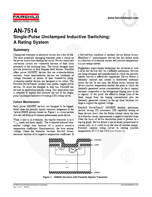
AN-7514Single-Pulse Unclamped Inductive Switching:A Rating SystemSummaryUnexpected transients in electrical circuits are a fact of life. The most potentially damaging transients enter a circuit on the power source lines feeding the circuit. Power control and conversion circuits are vulnerable because of their close proximity to the incoming lines. The circuit designer must provide protection or face frequent field failures. Fairchild offers power MOSFET devices that are avalanche-failure resistant. Some semiconductor devices are intolerant of voltage transients in excess of their breakdown rating. Avalanche-capable devices are designed to be robust. The Fairchild PowerTrench® product line typifies rugged power devices. To assist the designer in their use, Fairchild has devised an application-specific rating. This application note is intended to explain and illustrate the use of the single-pulse Unclamped Inductive Switching (UIS) rating curves. Failure MechanismsEarly power MOSFET devices, not designed to be rugged, failed when the parasitic bipolar transistor indigenous to the vertical DMOS process turned on. Figure 1 is a cross-section of a unit cell from an N-channel enhancement mode device. When a unit is in avalanche, the bipolar transistor is in a V CER mode and heats rapidly. The avalanche-induced base-emitter voltage rises because of a positive resistive temperature coefficient. Simultaneously, the base emitter voltage, where the transistor becomes forward biased, decreases because of its negative temperature coefficient. If a forward-bias condition is reached, device failure occurs. Blackburn’s[1] measurements showed that this failure mode is a function of avalanche current and junction temperature; it is not energy related.Ruggedness improvement technology has advanced to such a level that devices fail via a different mechanism. Devices are being designed and manufactured in which the parasitic bipolar turn-on is effectively suppressed. Device failure is thermally induced and current is distributed uniformly across the die. In this case, the failure occurs because the device junction temperature reaches the point at which the thermally generated carrier concentration (in the n- region) becomes comparable to the background doping (also in the n- region). At this point, the effective charge (sum of the fixed charge from the doping concentration plus the thermally generated carriers) in the epi layer becomes too large to support the applied voltage.Fairchild PowerTrench® MOSFET families epitomizes devices having UIS robustness. UIS capability testing of these devices shows that the failure current versus the time in avalanche closely approximates a negative one-half slope when the locus of device destruction point is plotted on a log-log graph. Device failure is not inversely proportional to current only, as it would be in the case of constant energy. Fairchild supplies rating curves at starting junction temperatures of 25°C and 150°C (see Figure 2).Figure 1. VDMOS Structure with Parasitic Bipolar TransistorFigure 2. FDB8444 Unclamped-Inductive-Switching SaferOperating Area Curve (Single-Pulse UIS SOA)Test Circuit EquationsThe circuit model (see Figure 3) used to describe a UIS test is a simple, lumped parameter series inductor / resistor circuit in which both the power supply and device avalanche voltage are presumed to be constant. All the equations that result from the mathematical analysis are listed in Table 1 by the V DD ; R conditions commonly referenced in the test method and commercial datasheets. The equations in row 1 are for the general case. The factor K is the ratio of the net voltage across the inductor and resistor to the resistor voltage drop. When K is large (K >30), the equations in row 1 reduce to those in rows 2 and 3. This can be accomplished mathematically by substituting the series expansion: ln (1+X) = X -X 2/2+. Only the first term is needed for t AV , while two terms are required for E AS and P AS(AVE). Time in avalanche, t AV , is the important parameter for a rugged device. Reviewing the expressions for t AV in Table 1, the following observations can be made:Series circuit resistance reduces the device avalanche stress. A supply voltage approaching the device avalanche voltage increases t AV . Stress increases and the allowable avalanche current is reduced.When the supply voltage is zero, t AV varies inversely with the device avalanche voltage.The equations of Table 1 presume that the device avalanche voltage is constant. In an actual test, it is not. Experiments have been performed using devices with similar low-current room temperature BV DSS readings. V DD , L, R, I AS , and t AV were carefully measured and the avalanche breakdown was calculated. All units yielded similar results. The effective avalanche voltage in all cases was 30% larger than BV DSS when avalanched near rated capability (see Figure 5 and Figure 6). V DSX(SUS) is the effective voltage referenced in the JEDEC test method [2]. Fairchild has chosen to list V DSX(SUS) in the t AV equations on the rating curves for these devices as 1.3 times the rated low-current breakdown voltage.I AS - peak current reached during device avalanche t AV - time duration of device avalancheV DSX(SUS) - effective (constant) device breakdown voltage during avalanche (approximately 1.3.BV DSS ) L - Inductance R - ResistanceV DD - output circuit supply voltageK - (V DSX(SUS)-V DD )/(I AS R) - ratio of the inductor plus the resistor voltage to the resistor voltage dropFigure 3. UIS Test CircuitFigure 4. UIS WaveformsTable 1. Mathematical AnalysisRow #Circuit Condition Time in AvalancheAvalanche EnergyAverage Avalanche Power V DD Rt AVE ASP AS(AVE)=(E AS /t rep ), t rep >t AV1 V DD R (L/R)ln(1+1/K) (LI AS V DSX(SUS)/R)[1–Kln(1+1/K)][I AS V DSX(SUS)].[(1/ln(1+1/K))-K)(t AV /t rep )2 V DD 0 LI AS /(V DSX(SUS)-V DD ) LI AS 2/[2(1-V DD /V DSX(SUS))] (I AS V DSX(SUS)/2)(t AV /t rep )3 0 0 LI AS /V DSX(SUS) LI AS 2/2 (I AS V DSX(SUS)/2)(t AV /t rep )‐50510152025‐55152535455500.00050.0010.00150.002A m p sV o l t sTime (s)VDS IDFigure 5. FDB8444 V DSX(SUS), L=5mH,I AS =5A, Initial T J =25°C‐50510152025‐5515253545550.0010.0020.0030.004A m p sV o l t sTime (s)VDS IDFigure 6. V DSX(SUS), L=5mH, I AS =20A, Initial T J =25°CSingle-point avalanche-energy ratings at T J = 25°C are not application speci fic nor are they useful for comparing similar devices offered by different manufacturers. To highlight the difficulty, a hypothetical example is in order.Application Example: Operating Margin for a Single-Pulse UIS EventDetermine the safe single-pulse avalanche current for an application that uses L = 1mH and V DD = 0V for Fairchild’s FDB8444. Datasheet information is as follows (reference the UIS rating curve in Figure 2): E AS = 307mJ Maximum T J = 25o C (Starting) BV DSS = 40V L = 200µHV DD = 0V during avalancheI AS = 56A (Effective I AS calculates to 55.4A because R ≠ 0Ω and a non-constant V DSX(SUS) as a result of self-heating, (see Figure 5)t AV = 477µs (calculated using effective IAS = 55.4A) Only a starting junction temperature of 25°C can be assessed. For a starting temperature other than that described in Fairchild datasheets (usually 25°C and 150°C), additional analysis is required to extrapolate the duration and amplitude limits of the avalanche event.Parasitic Bipolar Turn-onAssuming the parasitic bipolar transistor is suppressed, it need not be considered for state-of-the-art devices.Constant EnergyTo use the relationship E AS = L I 2AS /(2(1-V DD /V DSX(SUS))), use V DSX(SUS) = 1.3.BV DSS . For a constant energy of 307mJ, the predicted safe I AS (for L = 1mH) would equal 24.8A (t AV = 477µs). This data point is located beneath the 25°C Figure 2 UIS rating curve.Thermal (I 2AS t AV = Constant)T JS = 25°CAgain using V DSX(SUS) = 1.3.BV DSS in the relationship t AV = LI AS /( V DSX(SUS)-V DD ) for the intended application (L = 1mH), predicted t AV and I AS are: I 3AS = 0.654 (V DSX(SUS)-V DD )/L where: L = 1mH, V DD = 0V,V DSX(SUS) = 1.3.BV DSS , t AV = 623µs, and I AS = 32.4A.It is a simple matter to establish the safe avalanche current for a Fairchild PowerTrench ® devise when supplied with rating curves.T JS = 150°CDatasheet I 2AS t AV = 0.25. At the maximum rated starting junction temperature, t AV = 452µs and I AS = 23.5A. The safe avalanche current for any starting T J can be established from the Fairchild rating curves. Stoltenburg [3] showed that for avalanche-rated devices, avalanche failure was a linear function of starting T J for a fixed inductor. This is also true for a constant t AV . It is a simple matter then to establish the I 2AS t AV = constant for any starting T J . T JS = 100o C is a common operating temperature for a practical application. Entering the Fairchild curves at any convenient t AV , in this case; 0.6ms; the I AS temperature sensitivity is (20A-33A)/+125°C or -104mA/°C. Therefore, I AS = 33-(0.104) (100°C-25°C) = 25.2A for t AV = 0.6ms and I 2AS t AV = 0.381. For the example application where L = 1mH, using I 3AS = 0.381 (V DSX(SUS)-V DD )/L; a maximum avalanche current of I AS = 27.1A for a starting T J = 100°C.Related DatasheetsFor Fairchild documents available on the internet, see website [1] D. L. Blackburn, “Power MOSFET Failure Revisited,” Proc. 1988 IEEE Power Electronics Specialists Conference, pp681-688, April 1988.[2] “Single-Pulse Unclamped Inductive Switching (UIS) Avalanche Test Method,” JEDEC Standard JESD24-5, October2002.[3] Rodney R. Stoltenburg, “Boundary of Power-MOSFET, Unclamped Inductive-Switching (UIS) Avalanche-CurrentCapability,” Proc. 1989 Applied Power Electronics Conference, pp 359-364, March 1989.[4] Miroslav Glogolja, “Ruggedness Test-Claims Demand Another Careful Look,” Powertechnics Magazine, pp 23-28, July1986.[5] S. K. Ghandhi, Semiconductor Power Devices, John Wiley & Sons, New York, pp 15-29, 1977.DISCLAIMERFAIRCHILD SEMICONDUCTOR RESERVES THE RIGHT TO MAKE CHANGES WITHOUT FURTHER NOTICE TO ANY PRODUCTS HEREIN TO IMPROVE RELIABILITY, FUNCTION, OR DESIGN. FAIRCHILD DOES NOT ASSUME ANY LIABILITY ARISING OUT OF THE APPLICATION OR USE OF ANY PRODUCT OR CIRCUIT DESCRIBED HEREIN; NEITHER DOES IT CONVEY ANY LICENSE UNDER ITS PATENT RIGHTS, NOR THE RIGHTS OF OTHERS.LIFE SUPPORT POLICYFAIRCHILD’S PRODUCTS ARE NOT AUTHORIZED FOR USE AS CRITICAL COMPONENTS IN LIFE SUPPORT DEVICES OR SYSTEMS WITHOUT THE EXPRESS WRITTEN APPROVAL OF THE PRESIDENT OF FAIRCHILD SEMICONDUCTOR CORPORATION.As used herein:1. Life support devices or systems are devices or systemswhich, (a) are intended for surgical implant into the body, or(b) support or sustain life, or (c) whose failure to performwhen properly used in accordance with instructions for use provided in the labeling, can be reasonably expected toresult in significant injury to the user. 2. A critical component is any component of a life supportdevice or system whose failure to perform can bereasonably expected to cause the failure of the life support device or system, or to affect its safety or effectiveness.。
电气工程专业英语 (1)

电路 electric circuit电气工程electrical engineering 电机electric machine自然科学physical science电气设备 electrical device电器元件 electrical element正电荷positive charge负电荷negative charge直流direct current交流alternating current电压voltage导体conductor功work电动势electromotiveforce电势差potential difference功率power极性polarity能量守恒定律the law of conservation energy 变量variable电阻 resistance电阻率resistivity绝缘体insulator电阻器resistor无源元件passive element常数constant电导conductance短路short circuit开路open circuit线性的linear串联series并联parallel电压降voltage drop等效电阻equivalent resistance 电容器capacitor电感器inductor储能元件storage element电场electric field充电 charge放电discharge动态的dynamic电介质dielectric电容capacitance磁场magnetic field电源power supplu变压器transformer电机electric motor线圈coil电感inductance导线conducting wire绕组wingding漏电阻leakage resistance电子系统electronic system结构图block diagram功能模块functional block放大器amplifier滤波器filter整形电路wave-shaping circuit 振荡器oscillator增益gain输入阻抗input impedance带宽bandwidth晶体管transistor集成电路integrated circuit电力电子power electronics数字信号处理digital signal-processing 输出装置output device模拟信号analog signal数字信号digital signal传感器transducer采样值sample value模数转换器analog-to-digital converter 频谱frequency content采样频率sampling rate or frequendy扰动disturbance分立电路discrete circuit数字化信号digitized signal运算放大器operational amplifier有源电路active circuit电子部件electronic unit封装package管脚pin同相端noninverting terminal反相输入inverting input电路图circuit diagram压控电压源voltage-controlled voltage source 开环增益open-loop gain闭环增益closed-loop gain负反馈negative feedback正饱和positive saturation线性区linear region电压跟随器voltage follower等效阻抗equivalent impedance逻辑变量logic variable位bit数字字digital word字节byte半字节nibble与运算AND operation真值表truth table与门AND gate非门NOT gate或门OR gate加号addition sign与非门NANA gate异或运算XOR operation逻辑表达式logic expression 二进制binary system正逻辑positive logic负逻辑negative logic参考方向reference direction 理想变压器ideal transformer 电气绝缘electrical isolation阻抗匹配impedance matching电力electrical pewer绝缘变压器isolating transformer电压互感器voltage transformer电流互感器current transformer原边绕组primary winding工作频率operating frequency配电变压器distribution transformer 电力变压器power transformer磁通密度flux density磁场magnetic field铁芯变压器iron-core transformer大功率high-power空芯air-core磁耦合magnetic coupling小功率lower-power励磁损耗magnetizing loss磁滞损耗hysteresis loss涡流eddy current励磁电流exciting current漏磁通leakage flux互磁通 mutual flux线圈coil芯式core form壳式shell form高压绕组high-voltage winding 磁链flux linkage电动势electromotive force有效值root mean square value 匝数比turns ratio视在功率apparent power匝数the number of turns升压变压器step-up transformer 降压变压器step-down transformer 电动机motor发电机generator机械能mechanical energy电能electrical energy电磁的electromagnetic直线式电动机linear motor同步电机synchronous machine感应电机induction machine定子stator转子rotor气隙air gap轴shaft电枢armature励磁绕组field winding无功功率reactive power制动状态braking mode稳态steady-state相序phase sequence反响制动plugging滞后电流lagging current励磁电抗magnetizing reactance 启动电流starting current变频器frequency changer感应电势induced voltage逆变器inverter周波变换器cycloconverter换向器commutator自动控制automatic control控制器controller扰动disturbance期望值desired value压力pressure液位liquid level被控变量controlled variable 方框图block diagram传递函数transfer function 工程控制process control伺服系统servomechanism流率flow rate加速度acceleration前向通路forward path补偿correction反馈通路feedback path闭环closed-loop开环open-loop输出output增益gain手动调节manual adjustment变送器transducer误差error控制方式control mode比例控制proportional control 积分控制integral control微分控制derivative control 执行元件manipulating element 调节时间setting time残差residual error不确定度uncertainty观测数据observations采样sample算术平均arithmetic average 期望值expected value标准偏差standard deviation 下限lower range limit上限upper range limit跨度span分辨率resolution死区dead band灵敏度sensitivity阈值threshold可靠性reliability过量程overrange恢复时间recovery time过载overload过量程极限overrange limit 漂移drift准确性accuracy误差error重复性repeatability系统误差systemic error再现性reproducibility校准calibration线速度linear velocity角速度angular velocity弧度radian测速仪tachometer增量式编码器incremental encoder 定时计数器timed counter稳定性stability接口interface调节器conditioner开关switch执行器actuator电磁阀solenoid valve连续控制系统sequential control system 触点contact常开normally open常闭normally closed限位开关limit switch继电器relay延时继电器time-delay relay接通电流pull-in current开断电流drop-out current电机启动器motor starter接触器contactor自锁触点holding contact整流器rectifier变流器converter逆变器inverter二极管diode阳极anode阴极cathode正向偏置forward biased反向偏置reverse biased阻断block稳压二极管zener diode晶体管transistor集电极collector基极base发射极emitter共发射极common-emitter双向晶闸管triac正半周positive half-cycle 触发电流trigger circuit 功率容量power capability 功率器件power device晶闸管thyristor导通conduction正向阻断 forward-blocking通态on-state关断状态off-state反向击穿电压reverse breakdown voltage 漏电流leakage current电流额定值current rating漏极drain门极gate缓冲电路snubber circuit均流current sharing额定电压rated voltage可控开关controllable switch相控phase-controlled充电器charger工频line-frequency变换器converter整流rectification逆变inversion可逆调速revesible-speed再生制动regenerative barking关断时间turn-off time纯电阻负载pure resistive load脉动ripple感性负载inductance load周期time period带内部直流电动势的负载load witn an internal DC voltage 波形waveform换相commutation稳态steady state交流侧AC-side延时角delay angle交点intersection电力系统power system发电厂generating plant发电机generator负荷load输电网transmission nerwork 配电网distribution network 电electricity天然气natural gas原理图schematic diagram锅炉boiler热效率thermal efficiency 风力wind power断路器circuit breaker变电所substation故障fault过电压overvoltage击穿值breakdown value过电流over current可靠性reliability继电器relay触点contact电流互感器current transformer合闸线圈operating coil分闸线圈trip coilCircuit theory is also valuable to students specializing in other branches of the physical science because circuit are a good model for the study of energy system in general,and because of the applied mathematics,physics,and topology involved.电路理论对于专门研究自然科学其他分支的学生来说也十分有价值,因为电路一般可以很好地作为能量系统研究的模型,并且电路理论涉及应用数学、物理学和拓扑学的相关知识。
CELON+RFITT_+翻译件

治疗静脉曲张
CELON 静脉设备系统
双极 RF 电极 CELON ProCurve弯曲
消融设备 CELON Precision
Made in Germany
双极 RFITT 消融
注册商标: Radiofrequency-induced thermotherapy (RFITT®) 射频感应温热疗法
电极1
绝缘体
电极2
RFITT 温度
局部精确使用射频能量 使血管温和收缩封闭
在射频治疗时的温度是 60°C to 100°C.
3D 阻抗反馈
如果血管闭塞, 阻 抗声音信号增大,输出 功率自动停止
RFITT专利技术: 声音反馈监视阻抗.
在凝固过程中,功率自 动控制能量输出
超声影像of CELON ProCurve
系统特点
需要隐静脉穿刺
双极技术
任意选择静脉的 穿刺部位
自动控制停止功 能
3D阻抗反馈
60° to 100° C
临床结果
完全闭合率98,4 %... 到 99,6 % 有效的治疗方法被许多病人接受 RFA 相比“激光腔内消融”病人痛 苦小,对血管损伤轻,被认为是 很成功的治疗方法
Radiofrequency-induced thermal therapy: results of a European multicentre study of resistive ablation of incompetent truncal varicose veins. [Phlebology 2013 Feb;28(1):38-46] Laser and Radiofrequency Ablation Study (LARA study): A Randomised Study Comparing Radiofrequency Ablation and Endovenous Laser Ablation (810 nm) [Eur J Vasc Endovasc Sug. 2010 Aug;40(2)]
韩国先进科技学院机械工程系Bong Jae Lee副教授简介

Bong Jae LeeAssociate ProfessorThermal Radiation LaboratoryDepartment of Mechanical EngineeringKorea Advanced Institute of Science and Technology(KAIST)291Daehak-ro,Yuseong-guDaejeon305-701,Republic of KoreaEmail:bongjae.lee@kaist.ac.krPhone:+82-42-350-32391RESEARCH INTERESTS•Near-Field Thermal Radiation for Thermophotovoltaic Energy Conversion•Electric/Magnetic Metamaterials for Solar Energy Harvesting•Radiation Thermometry at Extreme Conditions2EDUCATION•Georgia Institute of Technology,Atlanta,Georgia,USA–Ph.D.,Mechanical Engineering2007/12–M.S.,Mechanical Engineering2005/08•Seoul National University,Seoul,Republic of Korea–B.S.,Mechanical Engineering2001/083PROFESSIONAL APPOINTMENTS•Associate Professor,KAIST2013/09–present •Assistant Professor,KAIST2011/05–2013/08•Assistant Professor,University of Pittsburgh2008/09–2011/04•Postdoctoral Fellow&Lecturer,Georgia Institute of Technology2008/01–2008/084HONORS AND A W ARDS•Best Paper Award,Thermal Engineering Division,KSME2015•Excellence in Teaching Prize,KAIST2015•Outstanding Teaching Award(MAE311Heat Transfer),Department of Mechanical Engineering, KAIST Spring2014•Invited Professor Grant,`Ecole Centrale Paris July,2014•Young Investigator Award,Thermal Engineering Division,KSME2014•Outstanding Teaching Award(MAE810Special Topic:Nanoscale Heat Transfer),Department of Mechanical Engineering,KAIST Spring2012•Sigma Xi(Georgia Tech Chapter)Best Ph.D.Thesis Award2008•ASME-Hewlett Packard Best Paper Award(2nd place)2007•Haiam Scholarship from the SeAH Steel Corporation1996–20015PUBLICATIONS5.1INTERNATIONAL JOURNAL1.M.Lim,S.S.Lee,and B.J.Lee,“Near-Field Thermal Radiation between Doped-Si Plates atNanoscale Gaps,”Physical Review B91,195136,2015(IF:3.664).2.M.Lim,S.M.Jin,S.S.Lee,and B.J.Lee,“Graphene-Assisted Si-InSb Thermophotovoltaic Devicefor Low Temperature Applications,”Optics Express23,A240–A253,2015(IF:3.525).3.S.Han and B.J.Lee,“Control of Thermal Radiative Properties using Two-Dimensional ComplexGratings,”International Journal of Heat and Mass Transfer83,713–721,2015(IF:2.522).4.J.Yeo,G.Kim,S.Hong,J.Lee,H.Park,B.J.Lee,C.P.Grigoropoulos,S.H.Ko,“Single NanowireResistive Nano-heater for Highly Localized Thermo-Chemical Reactions:Localized Hierarchical Heterojunction Nanowire Growth,”Small10,5015–5022,2014(IF:7.514).5.J.Jeon,S.Park,and B.J.Lee,“Optical Property of Blended Plasmonic Nanofluid based on GoldNanorods,”Optics Express22,A1101–A1111,2014(IF:3.525).6.B.J.Lee,Y.-B.Chen,S.Han,F.-C.Chiu,and H.J.Lee,“Wavelength-Selective Solar ThermalAbsorber with Two-Dimensional Nickel Gratings,”Journal of Heat Transfer136,072702,2014 (IF:2.055).7.H.Park,B.J.Lee,and J.Lee,“Note:Simultaneous Determination of Local Temperature andThickness of Heated Cantilevers using Two-Wavelength Thermoreflectance,”Review of Scientific Instruments85,036106,2014(Selected for RSI Editor’s Picks2014;IF:1.367).8.M.Lim,S.S.Lee,and B.J.Lee,“Near-Field Thermal Radiation between Graphene-Covered DopedSilicon Plates,”Optics Express21,22173–22185,2013(IF:3.525).9.J.S.Jin,B.J.Lee,and H.J.Lee,“Analysis of Phonon Transport in Silicon Nanowires IncludingOptical Phonons,”Journal of the Korean Physical Society63,1007–1013,2013(IF:0.506).10.B.Ding,M.Yang,B.J.Lee,and J.-K.Lee,“Tunable Surface Plasmons of Dielectric Core-MetalShell Particles for Dye Sensitized Solar Cells,”RSC Advances3,9690–9697,2013(IF:2.562). 11.J.Kim,S.Han,T.Walsh,K.Park,B.J.Lee,W.P.King,and J.Lee,“Temperature Measurementof Heated Microcantilever using Scanning Thermoreflectance Microscopy,”Review of Scientific Instruments84,034903,2013(IF:1.367).12.H.J.Lee,J.S.Jin,and B.J.Lee,“Assessment of Phonon Boundary Scattering from Light Scat-tering Standpoint,”Journal of Applied Physics112,063513,2012(IF:2.168).13.J.Lee,B.J.Lee,and W.P.King,“Deflection Sensitivity Calibration of Heated MicrocantileversUsing Pseudo-gratings,”IEEE Sensors Journal12,2666–2667,2012(IF:1.520).14.B.J.Lee,K.Park,T.Walsh,and L.Xu,“Radiative Heat Transfer Analysis in Plasmonic Nanoflu-ids for Direct Solar Thermal Absorption,”Journal of Solar Energy Engineering134,021009,2012 (IF:0.846).15.L.Xu,Z.-J.Zhang,and B.J.Lee,“Magnetic Resonances on Core-Shell Nanowires with Notches,”Applied Physics Letters99,101907,2011(Selected for the September19,2011issue of Virtual Journal for Nanoscale Science&Technology;IF:3.844).16.Z.-J.Zhang,K.Park and B.J.Lee,“Surface and Magnetic Polaritons on Two-DimensionalNanoslab-Aligned Multilayer Structure,”Optics Express19,16375–16389,2011(IF:3.587).17.B.Ding,B.J.Lee,M.Yang,H.S.Jung,and J.-K.Lee,“Surface-Plasmon Assisted Energy Con-version in Dye-Sensitized Solar Cells,”Advanced Energy Materials1,415–421,2011(IF:10.043).18.W.DiPippo,B.J.Lee,and K.Park,“Design Analysis of Surface Plasmon Resonance Immunosen-sors in Mid-Infrared Range,”Optics Express18,19396–19406,2010(Selected for the October 22,2010issue of Virtual Journal for Biomedical Optics;IF:3.753).19.L.Xu,B.J.Lee,W.L.Hanson,and B.Han,“Brownian Motion Induced Dynamic Near-FieldInteraction between Quantum Dots and Plasmonic Nanoparticles in Aqueous Medium,”Applied Physics Letters96,174101,2010(IF:3.841).20.A.J.McNamara,B.J.Lee,and Z.M.Zhang,“Quantum Size Effects on the Lattice Specific Heat ofNanostructures,”Nanoscale and Microscale Thermophysical Engineering14,1–20,2010(Figure selected as the cover image for the January2010issue;IF:1.903).21.S.Basu,B.J.Lee,and Z.M.Zhang,“Near-Field Radiation Calculated with an Improved DielectricFunction Model for Doped Silicon,”Journal of Heat Transfer132,021005,2010(IF:0.942). 22.S.Basu,B.J.Lee,and Z.M.Zhang,“Infrared Radiative Properties of Heavily Doped Silicon atRoom Temperature,”Journal of Heat Transfer132,021001,2010(IF:0.942).23.B.J.Lee and A.C.To,“Enhanced Absorption in One-dimensional Phononic Crystals with Inter-facial Acoustic Waves,”Applied Physics Letters95,031911,2009(IF:3.554).24.X.J.Wang,J.D.Flicker,B.J.Lee,W.J.Ready,and Z.M.Zhang,“Visible and Near-InfraredRadiative Properties of Vertically Aligned Multi-Walled Carbon Nanotubes,”Nanotechnology20, 215704,2009(IF:3.137).25.L.P.Wang,B.J.Lee,X.J.Wang,and Z.M.Zhang,“Spatial and Temporal Coherence of ThermalRadiation in Asymmetric Fabry-Perot Resonance Cavities,”International Journal of Heat and Mass Transfer52,3024–3031,2009(IF:1.947).26.B.J.Lee and Z.M.Zhang,“Indirect Measurements of Coherent Thermal Emission from a Trun-cated Photonic Crystal Structure,”Journal of Thermophysics and Heat Transfer23,9–17,2009 (IF:0.687).27.Q.Li,B.J.Lee,Z.M.Zhang,and D.W.Allen,“Light Scattering of Semitransparent SinteredPolytetrafluoroethylene(PTFE)Films,”Journal of Biomedical Optics13,054064,2008(IF:2.970).28.B.J.Lee and Z.M.Zhang,“Lateral Shift in Near-Field Thermal Radiation with Surface PhononPolaritons,”Nanoscale and Microscale Thermophysical Engineering12,238–250,2008(IF:1.000).29.B.J.Lee,L.P.Wang,and Z.M.Zhang,“Coherent Thermal Emission by Excitation of MagneticPolaritons between Periodic Strips and a Metallic Film,”Optics Express16,11328–11336,2008 (IF:3.880).30.Y.-B.Chen,B.J.Lee,and Z.M.Zhang,“Infrared Radiative Properties of Submicron Metallic SlitArrays,”Journal of Heat Transfer130,082404,2008(IF:1.421).31.B.J.Lee,Y.-B.Chen,and Z.M.Zhang,“Transmission Enhancement through Nanoscale MetallicSlit Arrays from the Visible to Mid-infrared,”Journal of Computational and Theoretical Nanoscience 5,201–213,2008(Invited paper;IF:1.256).32.B.J.Lee,Y.-B.Chen,and Z.M.Zhang,“Surface Waves between Metallic Films and TruncatedPhotonic Crystals Observed with Reflectance Spectroscopy,”Optics Letters33,204–206,2008 (Featured in the Year End Review issue of Aerospace America2008;IF:3.772).33.B.J.Lee,Y.-B.Chen,and Z.M.Zhang,“Confinement of Infrared Radiation to Nanometer Scalesthrough Metallic Slit Arrays,”Journal of Quantitative Spectroscopy and Radiative Transfer109, 608–619,2008(IF:1.635).34.B.J.Lee,K.Park,and Z.M.Zhang,“Energy Pathways in Nanoscale Thermal Radiation,”AppliedPhysics Letters91,153101,2007(Figure selected as the cover image for the October8, 2007issue;Introduced in the October30,2007issue of Nanomaterials News;IF:3.596).35.B.J.Lee and Z.M.Zhang,“Coherent Thermal Emission from Modified Periodic Multilayer Struc-tures,”Journal of Heat Transfer129,17–26,2007(IF:1.202).36.Z.M.Zhang and B.J.Lee,“Lateral Shift in Photon Tunneling Studied by the Energy StreamlineMethod,”Optics Express14,9963–9970,2006(IF:4.009).37.B.J.Lee and Z.M.Zhang,“Design and Fabrication of Planar Multilayer Structures with CoherentThermal Emission Characteristics,”Journal of Applied Physics100,063529,2006(IF:2.316). 38.B.J.Lee,C.J.Fu,and Z.M.Zhang,“Coherent Thermal Emission from One-dimensional PhotonicCrystals,”Applied Physics Letters87,071904,2005(Selected for the August22,2005issue of Virtual Journal of Nanoscale Science&Technology;IF:4.127).39.B.J.Lee,Z.M.Zhang,E.A.Early,D.P.DeWitt,and B.K.Tsai,“Modeling Radiative Properties ofSilicon with Coatings and Comparison with Reflectance Measurements,”Journal of Thermophysics and Heat Transfer19,558–569,2005(IF:0.665).40.B.J.Lee,V.P.Khuu,and Z.M.Zhang,“Partially Coherent Spectral Radiative Properties ofDielectric Thin Films with Rough Surfaces,”Journal of Thermophysics and Heat Transfer19, 360–366,2005(IF:0.665).41.K.Park,B.J.Lee,C.J.Fu,and Z.M.Zhang,“Study of the Surface and Bulk Polaritons with aNegative Index Metamaterial,”Journal of the Optical Society of America B22,1016–1023,2005 (IF:2.119).42.H.J.Lee,B.J.Lee,and Z.M.Zhang,“Modeling the Radiative Properties of SemitransparentWafers with Rough Surfaces and Thin-Film Coatings,”Journal of Quantitative Spectroscopy and Radiative Transfer93,185–194,2005(IF:1.685).5.2DOMESTIC JOURNAL1.S.Han,B.Choi,T.-H.Song,S.J.Kim,and B.J.Lee,“Experimental Investigation of VariableEmittance Material Based on(La,Sr)MnO3,”Transactions of the Korean Society of Mechanical Engineers B37,583–590,2013.2.D.Kim,S.Kim,S.Choi,B.J.Lee,and J.Kim,“Effect of Flame Radiative Heat Transfer inHorizontal-Type HRSG with Duct Burner,”Transactions of the Korean Society of Mechanical En-gineers B37,197–204,2013.5.3INTERNATIONAL CONFERENCE PROCEEDING1.H.Han and B.J.Lee,“Spectral Absorptance of Tandem Grating and Its Application for Solar En-ergy Harvesting,”ASME International Mechanical Engineering Congress and Exposition,Abstract No.IMECE2014-36694,Montreal,Canada,November14–20,2014.2.H.Han and B.J.Lee,“Tailoring Radiative Property of Two-Dimensional Complex Grating Struc-tures,”15th International Heat Transfer Conference,Paper No.IHTC15-9050,Kyoto,Japan,Au-gust10–15,2014.3.J.Jeon,S.Park,and B.J.Lee,“Absorption Coefficient of Plasmonic Nanofluids based on GoldNanorods,”2nd International Workshop on Nano-Micro Thermal Radiation:Energy,Manufactur-ing,Materials,and Sensing,Shanghai,China,June6–9,2014.4.M.Lim,S.S.Lee,and B.J.Lee,“MEMS-based Parallel Plate with Sub-micron Gap for MeasuringNear-field Thermal Radiation,”2nd International Workshop on Nano-Micro Thermal Radiation: Energy,Manufacturing,Materials,and Sensing,Shanghai,China,June6–9,2014(poster presen-tation).5.M.Lim,S.S.Lee,and B.J.Lee,“Theoretical Investigation of the Effect of Graphene on the Near-Field Thermal Radiation between Doped Silicon Plates,”ASME4th Micro/Nanoscale Heat and Mass Transfer International Conference,Abstract No.MNHMT2013-22033,Hong Kong,China, December11–14,2013.6.Y.-B.Chen,S.W.Han,F.-C.Chiu,H.J.Lee,and B.J.Lee,“Design a Wavelength-SelectiveAbsorber for Solar Thermal Collectors with Two-Dimensional Nickel Gratings,”ASME Summer Heat Transfer Conference,Paper No.HT2013-17288,Minneapolis,MN,USA,July14–19,2013.7.J.Kim,B.J.Lee,W.P.King,and J.Lee,“Optical Heating and Temperature Sensing of Heated Mi-crocantilever using Two-Wavelength Thermoreflectance,”10th International Workshop on Nanome-chanical Sensing,Stanford University,CA,USA,May1–3,2013(poster presentation).8.J.Kim,S.Han,K.Park,B.J.Lee,W.P.King,J.Lee,“DC and AC Electrothermal Charac-terization of Heated Microcantilevers using Scanning Thermoreflectance Microscopy,”26th IEEE International Conference on Micro Electro Mechanical Systems,Taipei,Taiwan,January20–24, 2013(poster presentation).9.H.J.Lee,J.S.Jin,and B.J.Lee,“Theoretical Investigation of Phonon Boundary Scatteringfrom One-Dimensional Rough Surfaces,”3rd International Forum on Heat Transfer,Paper No.IFHT2012-149,Nagasaki,Japan,November13–15,2012.10.B.J.Lee,“Electric and Magnetic Resonances on Isolated Nanostructure,”ASME3rd Micro/NanoscaleHeat and Mass Transfer International Conference,Abstract No.MNHMT2012-75078,Atlanta,GA, USA,March3–6,2012.11.K.Park,J.K.Lee,and B.J.Lee,“Investigating Laser-Induced Heating of Plasmonic Nanofluidsfor a Fast,High Throughput Polymerase Chain Reaction,”ASME3rd Micro/Nanoscale Heat and Mass Transfer International Conference,Abstract No.MNHMT2012-75127,Atlanta,GA,USA, March3–6,2012.12.B.J.Lee and K.Park,“Direct Solar Thermal Absorption using Blended Plasmonic Nanofluids,”ASME International Mechanical Engineering Congress and Exposition,Abstract No.IMECE2011-64067,Denver,CO,USA,November11–17,2011.13.Z.-J.Zhang,B.J.Lee,and K.Park,“Modeling Radiative Properties of Nanowire-Aligned Multi-layer Structures,”presented at Open Forum on Radiative Transfer and Properties for Renewable Energy Applications,14th International Heat Transfer Conference,Washington,D.C.,USA,Au-gust8–13,2010.14.W.DiPippo,B.J.Lee,and K.Park,“Development of Surface Plasmon Resonance Immuno-Sensorsat Mid-Infrared Range,”14th International Heat Transfer Conference,Paper No.IHTC14-22914, Washington,D.C.,USA,August8–13,2010.15.B.J.Lee,W.Hanson,and B.Han,“Plasmon-Enhanced Quantum Dot Fluorescence Induced byBrownian Motion,”ASME2nd Micro/Nanoscale Heat and Mass Transfer International Confer-ence,Paper No.NMHMT2009-18185,Shanghai,China,December18–21,2009.16.B.J.Lee and Z.-J.Zhang,“Investigation of the Effects of Nanostructures on Thermal Radiation inthe Near Field,”7th Asia-Pacific Conference on Near-Field Optics,Jeju,Korea,November25–27, 2009(poster presentation).17.A.J.McNamara,B.J.Lee,and Z.M.Zhang,“Reexamination of the Size Effect on the LatticeSpecific Heat of Nanostructures,”ASME International Mechanical Engineering Congress and Ex-position,Abstract No.IMECE2009-12388,Orlando,FL,USA,November13–19,2009(poster pre-sentation).18.W.DiPippo,B.J.Lee,and K.Park,“Theoretical Investigation of Tip-based Nanoscale InfraredSpectroscopy,”ASME Summer Heat Transfer Conference,Paper No.HT2009-88538,San Francisco, CA,USA,July19–23,2009.19.B.J.Lee and A.C.To“Periodic Nanostructure Patterning using Pulsed Laser Ablation in the NearField,”ASME Summer Heat Transfer Conference,San Francisco,CA,USA,July19–23,2009.20.A.C.To and B.J.Lee,“Multifunctional One-dimensional Phononic Crystal Structures ExploitingInterfacial Acoustic Waves,”2009MRS Spring Meeting,San Francisco,CA,USA,April13–17, 2009.21.S.Basu,B.J.Lee,and Z.M.Zhang,“Near-Field Radiation Calculated with an Improved DielectricFunction Model for Doped Silicon,”ASME International Mechanical Engineering Congress and Exposition,Paper No.IMECE2008-68314,Boston,MA,USA,October31–November6,2008.22.L.P.Wang,B.J.Lee,and Z.M.Zhang,“Metamaterials Using Magnetic Resonance between Pe-riodic Strips and a Metallic Film,”OSA Fall Optics and Photonics Congress:Plasmonics and Metamaterials,Rochester,NY,USA,October20–23,2008.23.B.J.Lee,L.P.Wang,X.J.Wang,and Z.M.Zhang,“Spatial and Temporal Coherent Emission froma Fabry-Perot Resonance Cavity,”ASME3rd Energy Nanotechnology International Conference,Jacksonville,FL,USA,August10–14,2008.24.B.J.Lee and Z.M.Zhang,“Energy Streamlines in Near-Field Thermal Radiation,”ASME Mi-cro/Nanoscale Heat Transfer International Conference,Paper No.MNHT2008-52210,Tainan,Tai-wan,January6–9,2008.25.Y.-B.Chen,B.J.Lee,and Z.M.Zhang,“Infrared Radiative Properties of Submicron MetallicSlit Arrays,”ASME International Mechanical Engineering Congress and Exposition,Paper No.IMECE2007-41268,Seattle,WA,USA,November11–15,2007.26.S.Basu,B.J.Lee,and Z.M.Zhang,“Infrared Radiative Properties of Heavily Doped Siliconat Room Temperature,”ASME International Mechanical Engineering Congress and Exposition, Paper No.IMECE2007-41266,Seattle,WA,USA,November11–15,2007(2nd Place in ASME -Hewlett Packard Best Paper Award).27.B.J.Lee,K.Park,and Z.M.Zhang,“Visualization of Energy Streamlines in Near-Field ThermalRadiation,”in Photogallery Heat Transfer Visualization,ASME-JSME Thermal Engineering and Summer Heat Transfer Conference,Vancouver,Canada,July8–12,2007.28.B.J.Lee,Y.-B.Chen,and Z.M.Zhang,“Indirect Measurements of Coherent Thermal Emissionfrom a Truncated Photonic Crystal Structure,”ASME-JSME Thermal Engineering and Summer Heat Transfer Conference,Paper No.HT2007-321303,Vancouver,Canada,July8–12,2007.29.B.J.Lee,Y.-B.Chen,and Z.M.Zhang,“Can Infrared Energy Be Focused to Nanometeric LengthScale?”ASME International Mechanical Engineering Congress and Exposition,Chicago,IL,USA, November5–10,2006.30.B.J.Lee,Y.-B.Chen,and Z.M.Zhang,“Measurements of Coherent Thermal Emission from PlanarMultilayer Structures,”ASME International Mechanical Engineering Congress and Exposition, Chicago,IL,USA,November5–10,2006(poster presentation).31.Z.M.Zhang and B.J.Lee,“What is Photon Tunneling?”ASME International Mechanical Engi-neering Congress and Exposition,Chicago,IL,USA,November5–10,2006.32.B.J.Lee and Z.M.Zhang,“Coherent Thermal Emission from Modified Periodic Multilayer Struc-tures,”ASME International Mechanical Engineering Congress and Exposition,Paper No.IMECE2005-82487,Orlando,FL,USA,November5–11,2005.33.B.J.Lee and Z.M.Zhang,“Temperature and Doping Dependence of the Radiative Properties ofSilicon:Drude Model Revisited,”Proceedings of the13th IEEE Annual International Conference on Advanced Thermal Processing of Semiconductors,pp.251–260,Santa Barbara,CA,USA,October 4–7,2005.34.B.J.Lee and Z.M.Zhang,“Rad-Pro:Effective Software for Modeling Radiative Properties inRapid Thermal Processing,”Proceedings of the13th IEEE Annual International Conference on Advanced Thermal Processing of Semiconductors,pp.275–281,Santa Barbara,CA,USA,October 4–7,2005.35.B.J.Lee,V.P.Khuu,and Z.M.Zhang,“Partially Coherent Spectral Radiative Properties ofDielectric Thin Films with Rough Surfaces,”37th AIAA Thermophysics Conference,Paper AIAA-2004-2466,Portland,OR,USA,June28–July1,2004.36.B.K.Tsai,D.P.DeWitt,E.A.Early,L.M.Hanssen,S.N.Mekhontsev,M.Rink,K.G.Kreider,B.J.Lee,and Z.M.Zhang,“Emittance Standards for Improved Radiation Thermometry during Ther-mal Processing of Silicon Materials,”9th International Symposium on Temperature and Thermal Measurements in Industry and Science,Cavtat-Dubrovnik,Croatia,June22–25,2004.37.H.J.Lee,B.J.Lee,and Z.M.Zhang,“Modeling the Radiative Properties of SemitransparentWafers with Rough Surfaces and Thin-Film Coatings,”4th International Symposium on Radiation Transfer,Istanbul,Turkey,June20–25,2004.38.K.Park,B.J.Lee,C.J Fu,and Z.M.Zhang,“Effect of Surface and Bulk Polaritons on theRadiative Properties of Multilayer Structures with a Left-Handed Medium,”ASME International Mechanical Engineering Congress and Exposition,Washington D.C.,USA,Paper No.IMECE2003-41972,November16–21,2003.39.Z.M.Zhang,B.J.Lee,and H.J.Lee,“Study of the Radiative Properties of Silicon-Based Materialsfor Thermal Processing and Control,”Proceedings of the11th IEEE Annual International Con-ference on Advanced Thermal Processing of Semiconductors,pp.107–115,Charleston,SC,USA, September23–26,2003.40.B.J.Lee and Z.M.Zhang,“Development of Experimentally Validated Optical Property Models forSilicon and Related Materials,”Proceedings of the11th IEEE Annual International Conference on Advanced Thermal Processing of Semiconductors,pp.143–150,Charleston,SC,USA,September 23–26,2003.41.H.J.Lee,B.J.Lee,and Z.M.Zhang,“Modeling the Directional Spectral Radiative Properties ofSemitransparent Wafers with Thin-Film Coatings,”15th Symposium on Thermophysical Proper-ties,Boulder,CO,USA,June22–27,2003.5.4DOMESTIC CONFERENCE PROCEEDING1.J.Jeon,S.Park,and B.J.Lee,“Enhancing Light Absorption Performance of Volumetric So-lar Collector using Plasmonic Nanofluid based on Gold Nanorod,”KSME Annual Fall Meeting, Gwangju,Korea,November11–13,2014.2.M.Lim,S.M.Jin,S.S.Lee,and B.J.Lee,“Doped Si-Graphene-InSb Near-Field Thermophoto-voltaic System,”KSME Annual Fall Meeting,Gwangju,Korea,November11–13,2014.3.J.B.Kim and B.J.Lee,“Thermal Properties of Dielectric Nanofluids,”KSME Annual Fall Meet-ing,Gwangju,Korea,November11–13,2014.4.M.K.Lim,S.S.Lee,and B.J.Lee,“The Effect of Graphene on the Near-Field Radiation,”KSMEThermal Engineering Division Spring Meeting,Busan,Korea,May23–24,2013(poster presenta-tion).5.S.W.Kim and B.J.Lee,“Pool Boiling Characteristics of SiO2-Nanoparticle-Coated Surface,”KSME Thermal Engineering Division Spring Meeting,Busan,Korea,May23–24,2013.6.S.Han,H.J.Lee,and B.J.Lee,“Design and Analysis of Efficient Solar Absorber Using Two-Dimensional Metallic Gratings,”KSME Annual Fall Meeting,Changwon,Korea,November7–9, 2012.7.H.J.Lee,J.S.Jin,and B.J.Lee,“Specularity Models to Account for Energy Scattering by Sur-face Roughness,”KSME Thermal Engineering Division Spring Meeting,Yongpyung,Korea,May 23–25,2012.5.5BOOK CHAPTER1.Z.M.Zhang and B.J.Lee,“Theory of Thermal Radiation and Radiative Properties,”Chapter3,pp.74–132,in Radiometric Temperature Measurements:I.Fundamentals,Z.M.Zhang,B.K.Tsai, and G.Machin(eds.),Academic Press(an Imprint of Elsevier),Amsterdam,2009.5.6PATENT1.J.Jeon and B.J.Lee,“Plasmonic Nanofluid Having Broad-band Absorption Characteristic Madeby Blending Gold Nanorods of Different Aspect Ratios and Its Design Method,”Korea Patent (Application Number:10-2015-0000500).2.J.B.Kim and B.J.Lee,“Low Viscous Dielectric Nanofluid for Electric Device Cooling,”KoreaPatent(Application Number:10-2014-0173068).3.H.Lee,H.J.Choi,and B.J.Lee,“Metamaterial-based Absorber of Solar Radiation Energy andMethod of Manufacturing the Same,”Korea Patent(Patent Number:10-1497817).4.S.W.Han,B.S.Choi,T.H.Song,S.J.Kim,and B.J.Lee,“Thin Film of Variable Emittance Ma-terial on Metal Layer and Method for Fabrication,”Korea Patent(Patent Number:10-1430222).6INVITED PRESENTATIONS1.“Application of Thermal Radiation to Energy Technology,”Department seminar,Department ofMechanical Engineering,Pohang University of Science and Technology,Korea,May8,2015.2.“Introduction to Nanoscale Thermal Radiation,”Department seminar,School of Mechanical En-gineering,Yeungnam University,Korea,March27,2015.3.“Introduction to Nanoscale Thermal Radiation,”Group seminar,Thermal&Fluid System R&BDGroup,Korea Institute of Industrial Technology(KITECH),Korea,March17,2015.4.“Introduction to Nanoscale Thermal Radiation,”Department seminar,Department of MechanicalEngineering,Korea University,Korea,March6,2015.5.“Nanoscale Thermal Radiation:Theory and Application,”Division seminar,School of Energy Sci-ence and Engineering,Harbin Institute of Technology,Harbin,China,January19,2015.6.“Nanoscale Thermal Radiation:Theory and Application,”Division seminar,Institute of FluidScience,Tohoku University,Sendai,Japan,January13,2015.7.“Design of Metamaterial-based Solar Thermal Absorber,”Invited presentation,Material ResearchSociety of Korea,Daejeon,Korea,November27,2014.8.“Tailoring Radiative Properties with Micro/Nanostructures for Energy Harvesting,”Departmentseminar,Department of Mechanical Engineering,Yonsei University,Korea,November7,2014.9.“Tailoring Radiative Properties with Micro/Nanostructures for Energy Harvesting,”Departmentseminar,School of Mechanical and Advanced Material Engineering,Ulsan National Institute of Science and Technology,Korea,October15,2014.10.“Nanoscale Thermal Radiation:Theory and Application,”KCC open seminar,KAIST Institutefor Nanocentury,Korea,October14,2014.11.“Spectral and Directional Control of Radiative Properties using Nanostructures,”Departmentseminar,EM2C Laboratory,`Ecole Centrale Paris,France,July10,2014.12.“Application of Nanostructures in Solar Energy Absorption,”Invited presentation,KSME ThermalEngineering Division Spring Meeting,Jeju,Korea,April25,2014.13.“Designing Nanostructures for Solar Thermal Absorption,”Department seminar,School of Mecha-tronics,Gwangju Institute of Science and Technology,Korea,April16,2014.14.“Introduction to Nanoscale Thermal Radiation,”Division seminar,Division of Future Vehicle,KAIST,Korea,April9,2014.15.“Harvesting Solar Thermal Energy using Nanoscale Engineering,”Department seminar,Depart-ment of Materials Science and Engineering,Korea University,Korea,May25,2013.16.“Measurement of Radiative Properties and Their Control using Nanostructures,”Division seminar,Environmental and Energy Systems Research Division,Korea Institute of Machinery&Materials(KIMM),Korea,February7,2013.17.“Metamaterials for Thermal Radiation and Their Counterpart for Acoustic Waves and Phonons,”Department seminar,Department of Nano Manufacturing Technology,Korea Institute of Machin-ery&Materials(KIMM),Korea,February5,2013.18.“Plasmonic Nanoparticles for Energy and Sensing Applications,”Department seminar,Departmentof Mechanical Engineering,National Cheng Kung University,Taiwan,January25,2013.19.“Thermal Radiative Properties of Nanostructures,”Invited presentation,KSME Annual Fall Meet-ing,Changwon,Korea,November8,2012.20.“Tailoring Radiative Properties using Nanostructures,”Department seminar,Satellite Thermal/PropulsionDepartment,Korea Aerospace Research Institute(KARI),Korea,August29,2012.21.“Application of Gold Nanoshell for Biosensing and Direct Solar Thermal Absorption,”Invitedpresentation,Collaborative Conference on Materials Research,Seoul,Korea,June26,2012.22.“Thermal Radiative Properties of Nanostructures,”Department seminar,Department of Mechan-ical Engineering,Tokyo Metropolitan University,Japan,March16,2012.23.“Thermal Radiative Properties of Nanostructures,”Department seminar,Department of Mechan-ical Engineering,Tokyo University of Science,Japan,March15,2012.24.“Recent Development in Measurement Techniques of the Radius of Curvature of Reflectors inSolar Thermal Power Plant,”Department seminar,Department of Solar Energy,Korea Instituteof Energy Research(KIER),Korea,February29,2012.25.“Theory of Thermal Radiation&Radiative Properties,”Invited seminar,Home Appliance R&DLaboratory,LG Electronics,Korea,December16,2011.26.“Electric or Magnetic Metamaterials for Applications in Biosensing and Energy Harvesting,”Di-vision seminar,Nano-Mechanical Systems Research Division,Korea Institute of Machinery&Ma-terials(KIMM),Korea,November25,2011.27.“Application of Plasmonic Nanostructures in Solar Energy Harvesting,”KAIST Institute Thursdayseminar,KAIST Institute for Eco-Energy,Korea,October6,2011.28.“Localized Surface Plasmon and Its Applications in Biosensing and Energy Harvesting,”Depart-ment seminar,Department of Mechanical Engineering,Sogang University,Korea,May6,2011.29.“Tailoring Radiative Properties using Nanostructures,”Department seminar,Department of Me-chanical Engineering and Applied Mechanics,University of Pennsylvania,USA,November11, 2010.30.“Enhanced Fluorescence of Quantum Dots by the Dynamic Near-Field Interaction with PlasmonicNanoparticles,”Invited presentation,Workshop on Thermal Transport at the Nanoscale,Telluride, CO,USA,June21-25,2010.31.“Engineering Nanostructures for Tailoring Energy Transport,”Department seminar,Departmentof Physics,Indiana University of Pennsylvania,USA,April2,2010.32.“Nanostructures for the Control of Thermal Radiative Properties,”Invited presentation,ASMEMicro/Nanoscale Heat and Mass Transfer International Conference,Shanghai,China,December 18-21,2009.33.“Controlling Energy Transport using Surface Waves,”Department seminar,School of Informationand Communication Engineering,Inha University,Korea,May21,2009.34.“Controlling Energy Transport using Surface Waves,”Department seminar,School of Mechanicaland Aerospace Engineering,Seoul National University,Korea,May19,2009.35.“Controlling Energy Transport using Surface Waves,”Department seminar,School of Mechanicaland Advanced Material Engineering,Ulsan National Institute of Science and Technology,Korea, May15,2009.36.“Controlling Energy Transport using Surface Waves,”Department seminar,Department of Me-chanical Engineering,Kyung Hee University,Korea,May12,2009.37.“Coherent Thermal Emission from Nanostructures and Near-Field Radiative Heat Transfer,”De-partment seminar,Department of Mechanical Engineering,University of Massachusetts Lowell, USA,November6,2008.38.“Multilayer Structures for Coherent Thermal Emission and Energy Pathways in Near-Field Ra-diative Transfer,”Invited presentation,6th Japan-US Joint Seminar on Nanoscale Transport Phe-nomena-Science and Engineering,Boston,MA,USA,July13-16,2008.39.“Spectral and Directional Radiative Properties of Semitransparent Materials with Rough Sur-faces,”Division seminar,Optical Technology Division,Physics Department,National Institute of Standards and Technology,USA,November10,2004.7PROFESSIONAL ACTIVITIES&AFFILIATIONS7.1DEPARTMENTAL SER VICE•Curriculum Committee(2013–present)•Coordinator,KAIST-ITB Joint Workshop on Research and Education(2012–present)•Student Affairs Committee(2011–present)•Mechanical Engineering Design Competition Committee(Ad Hoc;2013–present)•EAC Preparation Committee(Ad Hoc;2014)。
《电工学》中英名词对照表

学习好资料欢迎下载《电工学》中英名词对照表一阶电路first-order circuitV形曲线V curve三相电路three-phase circuit三相功率three-phase power三相三线制three-phase three-wire system三相四线制three-phase four-wire system三相变压器three-phase transformer三角形联接trianular connection三角波triangular wave三相异步电动机three-phase induction motor 支路branch支路电流法branch current method中性点neutral point中性线neutral conductor中央处理器centre processing unit(CPU)互感mutual inductance介电常数permittivity of the dielectric瓦特Watt功率表powermeter无功功率reactive power韦伯Weber反电动势counter emf反相opposite in phase反馈控制feedback control方框图block diagram开路open circuit开关switch水轮发电机water-wheel generator功work功率power功率因数power factor功率三角形power triangle功率角power angle电能electric energy电荷electric charge电场electric field电场强度electric field intensity电位electric potential电位差electric potential difference 电位升potential rise电位降potential drop电位计potentiometer电压voltage电压三角形voltage triangle电动势electromotive force(emf)电源source电压源voltage source电流源current source电路circuit电路分析circuit analysis电路元件circuit element电路模型circuit model电流current电流密度current density电流互感器current transformer电阻resistance电阻器resistor电阻性电路resistive circuit电阻率resistivity电导conductance电导率conductivity电容capacitance电容器capacitor电容性电路capacitive circuit电感inductance电感器inductor电感性电路inductive circuit电桥bridge电机electric machine电磁转矩electromagnetic torque电角度electrical degree电枢armature电枢反应armature reaction电工测量electrical measurement电磁式仪表electromagnetic instrument 电动式仪表electrodynamic instrument 平均值average value平均功率average power正极positive pole正方向positive direction正弦量sinusoid正弦电流sinusoidal current结点node结点电压法node voltage method对称三相电路symmetrical three-phase circuit 主磁通main flux外特性external characteristic发送机transmitter他励发电机separately excited generator可编程控制器programmable controller(PLC)安培Ampere电流表currenter安匝ampere-turns伏特V olt电压表valeage伏安特性曲线volt-ampere characteristic有效值effective value有功功率active power交流电路alternating current circuit (a-ccircuit) 交流电机alternating-current machine自感self-inductance自感电动势self-induced emf自耦变压器autotransformer自励发电机self-excited generator自整角机selsyns自动控制automatic control自动调节automatic regulation自锁self-locking负极negative pole负载load负载线load line负反馈negative feedback动态电阻dynamic resistance并联parallel connection并联谐振parallel resonance并励发电机shunt d-c generator并励电动机shunt d-c motor并励绕组shunt field vending同步发电机synchronous generator同步电动机synchronous motor 同步转速synchronous speed同相in phase机械特性torque-speed characteristic过励overexcitation执行元件servo-unit传递函数transfer function传感器transducer闭环控制closed loop control回路loop网络network导体conductor导纳admittance阶跃电压step voltage全电流定律law of total current全响应complete response麦克斯韦Maxwell基尔霍失电流定律Kirchhof f’s current law (KCL)基尔霍失电压定律Kirchhof’s voltage law(KVL)库仑Coulomb亨利Henry角频率angular frequency串联series connection串联谐振series resonance串励绕组series field winding阻抗impedance阻抗三角形impedance triangle阻转矩counter torque初相位initial phase时间常数time constant时域分析time domain analysis时间继电器time-delay relay励磁电流exciting current励磁机exciter励磁绕组field winding励磁电流exciting current励磁变阻器field rheostat两相异步电动机two-phase induction motor两功率表法two-powermeter method伺服电动机servomotor步进电动机stepping motor步距角stepangle汽轮发电机turboalternator直流电路direct current circuit (d-c cir-cuit)直流电机direct-current machine法拉Farad空载no-load空载特性open-circuit characteristic空气隙air gap非线性电阻nonlinear resistance非正弦周期电流nonsinusoidal periodic受控电源controlled source变压器transformer变比ration of transformation变阻器rheostat线电压line voltage线电流line current线圈coil线性电阻linear resistance周期period参考电位reference potential参数parameter视在功率apparent power定子stator转子rotor转子电流rotor current转差率slip转速speed转矩torque组合开关switchgroup制动braking单相异步电动机single-phase induction motor 相phase相电压phase voltage相电流phase current相位差phase difference相位角phase angle相序phase sequence相量phasor相量图phasor diagram响应response星形联接star connection复数complex number阻抗impedance 导纳admittance复励发电机compound d-c generator欧姆Ohm欧姆定律Ohm's law等效电路equivalent circuit品质因数quality factor绝缘insulation绝缘体insulator显极转子salient poles rotor测速发电机tachometer generator绕组winding绕线式转子wound rotor起动starting起动电流starting current起动转矩starting torque起动按钮start button容抗capacitive reactance容纳capacitive susceptance诺顿定理Norton's theorem高斯Gauss原动机prime mover原绕组primary winding铁心core铁损core loss矩形波rectangular wave特征方程characteristic equation积分电路integrating circuit效率efficiency振荡放电oscill tory discharge继电器relay热继电器thermal overload relay(OLR)换向器commutator调节特性regulating characteristic调速speed regulation继电接触器控制relay-contactor control 副绕组secondary winding铜损copper loss基波fundamental harmonic谐波harmonic谐振频率resonant frequency通频带bandwidth理想电压源ideal voltage source理想电流源ideal current source减幅振荡attenuated oscillation常开触点normally open contact常闭触点normally closed contact停止stopping停止按钮stop button接收机receiver接触器contactor控制电动机control motor控制电路control circuit旋转磁场rotating magnetic field隐极转子nonsalient poles rotor涡流eddy current涡流损耗eddy-current loss焦耳Joule奥斯特Oersted短路short circuit锯齿波sawtooth wave幅值amplitude最大值maximum value最大转矩maximum(breakdown)torque 滞后lag超前lead傅里叶级数Fourier series暂态transient state暂态分量transient component等幅振荡unattenuated oscillation联锁interlocking感抗inductive reactance感纳inductive susceptance感应电动势induced emf楞次定则Lenz's law频率frequency频域分析frequency domain analysis频谱spectrum输入input输出output微法microfarad微分电路differentiating circuit叠加原理superposition theorem零状态响应zero-state response零输入响应zero-input response 罩极式电动机shaded-pole motor滑环slip ring鼠笼式转子squirrel-cage rotor截止角频率cutoff angular frequency 滤波器filters磁场magnetic field磁场强度magnetizing farce磁路magnetic circuit磁通flux磁感应强度flux density磁通势magnetomotive force(mmf)磁阻reluctance磁导率permeability磁化magnetization磁化曲线magnetization curve磁滞hysteresis磁滞回线hysteresis loop磁滞损耗hysteresis loss磁极pol磁电式仪表magnetoelectric instrument 漏磁通leakage flux漏磁电感leakage inductance漏磁电动势leakage emf赫兹Hertz稳态steady state稳态分量steady state component静态电阻static resistance碳刷carbon brush额定值rated value额定rated voltage额定功率rated power额定转矩tated torque瞬时值instantaneous value戴维宁定理Thevenin's theorem激励excitation满载full load槽fuse熔断器fuse。
反向电动势英语

Reverse electromotive force (EMF), also known as back EMF, is a crucial concept in the realm of electrical engineering and electromagnetism. It arises when an electric motor or generator is operated under dynamic conditions, fundamentally altering the behavior of these devices and their interactions with external circuits. This essay presents a comprehensive, multi-faceted analysis of reverse EMF, delving into its underlying principles, practical implications, and applications across various domains.I. Fundamentals of Reverse Electromotive ForceA. Definition and OriginsReverse EMF is a voltage that opposes the applied voltage in an electric circuit, particularly in motors and generators. It is generated as a result of Faraday's Law of Electromagnetic Induction, which states that a change in magnetic flux through a conducting loop induces an electromotive force (EMF) in the loop proportional to the rate of change of flux. In the context of electric motors, when the rotor (containing conductive windings) rotates within a magnetic field, it cuts through the lines of magnetic flux, producing an induced EMF. This induced EMF acts in opposition to the supply voltage, hence the term "reverse" or "back" EMF.B. Mathematical RepresentationMathematically, the magnitude of reverse EMF can be expressed as:E_{back} = k \cdot \omega \cdot \phiwhere E_{back} is the back EMF, k is a constant dependent on the motor's design (number of turns, winding configuration, etc.), ωis the angular velocity of the rotor, and φ is the magnetic flux density. This equation reveals that the back EMF is directly proportional to the rotor speed and the strength of the magnetic field.C. Role in Motor Operation1. **Torque-Speed Relationship:** The presence of back EMF significantly impacts the torque-speed characteristic of a motor. As the rotor accelerates, the back EMF increases, counteracting the applied voltage. This reduces the netvoltage available for driving current through the windings, consequently decreasing the torque produced by the motor. The result is a nonlinear relationship between torque and speed, often approximated by the following equation:T = K_t \cdot (V - E_{back}) \cdot Iwhere T is the torque, K_t is a torque constant, V is the applied voltage, and I is the current. This equation illustrates that at higher speeds, a larger portion of the applied voltage is opposed by back EMF, leading to a decline in torque output.2. **Efficiency and Power Consumption:** Back EMF contributes to the efficiency of electric motors by reducing power consumption at high speeds. Since the opposing voltage decreases the current drawn from the supply, the power loss due to resistive heating in the windings is minimized. This results in a more efficient operation, especially in applications where steady-state operation at high speeds is desired.II. Practical Implications and ApplicationsA. Motor Control Systems1. **Speed Control:** Understanding and accurately predicting back EMF is vital in designing effective motor control systems. By measuring or estimating the back EMF, controllers can adjust the applied voltage or current to maintain a desired speed or torque output, ensuring precise control over motor performance.2. **Braking and Regenerative Braking:** Back EMF enables motoring and generating modes in electric machines. When a motor is forced to decelerate (e.g., by mechanical load or external braking), the kinetic energy of the rotor can be converted back into electrical energy through the reverse EMF. This process, known as regenerative braking, allows for energy recovery and can significantly improve overall system efficiency in applications like electric vehicles and elevators.B. Protection against OvercurrentBack EMF serves as a natural protection mechanism against excessive currents in electric motors. At startup, when the rotor is stationary, there is no back EMF, allowing a large initial current to flow and generate the required torque to overcome static friction. As the motor accelerates, the back EMF increases, limiting the current and preventing overheating or damage due to excessive current draw.III. Advanced Topics and Research DirectionsA. High-Speed Motors and Electrical MachinesIn modern high-speed motors and electrical machines, the effects of back EMF become even more pronounced. Researchers are continually exploring advanced materials, cooling techniques, and electromagnetic designs to mitigate the negative impacts of high back EMFs, such as increased insulation stress and reduced thermal stability, while exploiting their benefits for enhanced efficiency and power density.B. Sensorless Control and Estimation TechniquesAccurate estimation of back EMF is crucial for sensorless control schemes, which eliminate the need for costly position or speed sensors in electric motors. Various techniques, such as high-frequency signal injection, Kalman filtering, and adaptive observers, have been developed to estimate back EMF in real-time, enabling efficient and reliable control without direct feedback from sensors.C. Energy Harvesting and MicrogeneratorsReverse EMF plays a central role in energy harvesting applications using microgenerators, piezoelectric transducers, or other vibration-powered devices. These systems exploit the reverse EMF generated by the relative motion between magnets or coils to convert ambient mechanical energy into usable electrical power, paving the way for self-powered wireless sensors, wearable electronics, and other autonomous devices.IV. ConclusionReverse electromotive force, a manifestation of Faraday's Law of Electromagnetic Induction, is a fundamental concept with far-reachingimplications in the realms of electric motors, generators, and related control systems. Its influence on torque-speed characteristics, efficiency, and power consumption makes it a critical factor in the design, operation, and optimization of these devices. Moreover, ongoing research and advancements in materials science, control strategies, and energy harvesting technologies continue to expand our understanding and utilization of reverse EMF, further solidifying its importance in the ever-evolving landscape of electrical engineering and electromagnetism.。
防静电简介
d:5mm d:10mm d:15mm d:20mm d:25mm
Ground Cable
measurement area is 25mm φ (at measurement distance 5mm)
Handy Type ESVM Demonstration 1
Model520-1 ESVM
①
②
Status of Electrostatic Removable / Irremovable
例1
例2
Electrostatic Generations
• 1. 2. 3. • Characteristic of Charge Tribo Charge Separations Charge Induced Charge Triboelectric Series
例2
5P Probe
Measurement Example (Conductive Floor/Tablemat)
Ground to Surface Point to Point Surface Resistance
Measurement Condition
1.Electrode Area 2.Electrode Figure 3.Pressure 4.Temperature 5.Humidity 6.Applied Voltage
Coulomb Meter (Electric Current Integral Calculus ).
Charged Material Probe
R
Coulomb Meter
Q C
V
V
C0 :Unknown
V1 ≒ Q1 / C1
Q1 = C1 Q C0 + C1
雷电防护科学与技术专业英语单词整理

……重要而又不可分割的一部分 a critical and integral part of 安全通道,逃逸通道escape route保安装置crowbar device爆裂explosive fracture北半球northern hemisphere被认为是陈旧的be considered obsolete避雷杆几何形状rod geometry标准,规范norm标准/扩展格式standard/extended format颮线Squall line不间断供电系统no break power systems财产Property n.测试波形test wave shapes插座receptacles n.承受Sustain v.尺寸,大小dimensions n.充气放电器gas-tube arrester穿孔puncture n.传导电流Conduct current磁屏蔽magnetic shield大体的区域 a general area单站,单点one location/single location导弹发射井missile silo等电位equipotentialization等电位联结equipotential bonding等雷暴的isokeraunic等值线图contour map低电阻值,低阻的low-resistance电层Coulomb n.电层Electrosphere n.电场electric field电磁场electromagnetic fields电动力学的electrodynamic a.电感性耦合inductive coupling电离通道Ionized path电离通道Ionized path电力公司electric power company电力线路electricity mains电偶极子electric dipoleIEEE(institule of electrical and 电气和电子工程师协会electronics engineers)电气系统与电子系统electrical and electronic systems 电势差Potential difference电线杆utility poles电信公司telecommunications company 电压钳位器voltage clamp电涌保护器surge protective device电涌放电器,防止过载放电器surge arrester电晕放电corona discharge电阻率Resistivity n.电阻率Resistivity n.电阻性耦合resistive coupling电阻值Resistance n.独立接闪器separate air terminal 对……敏感sensitive to对……由免疫能力immune to对流活动Convective activity发电装置generating sets法兰的非金属垫圈not metallic gasket of flange 防雷法规/规范Lightning protection code防雷装置lightning protection system 妨碍,干扰interfere with放电Discharge放电,电流泄放electrical discharges分流diversion风速计,风速表anemometer n.风险评估Risk assessment负电荷Negative charge感测装备sensing equipment感应电压induced voltage钢架结构基础foundation steelwork钢筋混凝土reinforced concrete高风险High risk隔离变压器isolation transformer隔离距离separation distance供应品,备用品provision n.故障,不工作malfunction故障自检系统automatic failure detection system 关联relevance观点,说明scenario过电流overcurrents过电压overvoltage过渡点transition point寒冷气候cold climates换能器,变换器transducer n.回击return stroke回击Return stroke毁灭性雷击catastrophic lightning strikes混凝土concrete火花塞spark火警装置fire alarm installation击中Strike v.&n.机械损伤mechanical damage积雨云Cumulonimbus基于……的观点with one's view即将来临的雷电先导imminent lightning leader 假想的Hypothetical a.坚固的建筑物substantial building箭式先导dart leader降水单体Rain cell接触电压touch voltage接触电压与跨步电压touch and step voltages 接地装置Earth temination system 接地装置grounding system接闪器air terminal接闪装置air termination system 结果是turn out to be解体,非集成disintegrate金属导管metal duct金属顶轿车metal-topped vehicle金属接地体grounding metal bodies金属氧化物变阻器metal oxide varistor(mov)进线incoming line绝缘insulation n.绝缘insulation n.绝缘关节insulating joint可控硅整流器silicon controlled rectifier(scr)空间分辨率spatial resolution跨步电压step voltage拦截,截取intercept v.浪涌电流surge current浪涌抑制器surge suppresser雷,雷声Thunder雷暴thunderstorm雷暴日thunderday雷暴日等值线图thunderday map=isokeraunic map 雷暴云thunderstorm cloud雷达反射率radar reflectivity雷电定位Thunder ranging雷电探测技术lightning detection technology雷电预报lightning prediction雷击可能性The potential of a lightning strike雷雨云Thundercloud连接端子,连接导体bonding conductor连续金属屏蔽continuous metallic screen流动贮藏系统fluid storage systems龙卷风tornado轮叶,风向标vane n.美国保险商实验所UL(Underwriters laboratories Inc.)NLDN=national lightning detection 美国电力雷电监测网network灭火装置fire extinguishing installation敏感电子设备sensitive electronics魔法magic bullet内心的平静peace of mind牛栏cow barn蓬松积云fluffy cumulus cloud屏蔽screen屏蔽shielding齐纳二极管Zener diode铅制品plumbing强硬的stiff a.强硬的要求stiff requirements球形电容器Spherical capacitor曲率,弯曲curvature n.确切的时间和位置exact time and place热效应thermal effect人工触发机制,人工引雷机制artificial trigger mechanism人工观测human observation熔化掉melt down冗余,备用redundancy n.入口处,入口点entrance point三端双向可控硅开关元件triac n.闪电高发区high lightning areas闪电接闪器lightning air terminal闪电频率Lightning frequency闪电频数Lightning frequency闪电频数剧烈区,闪电重发区servere lightning frequency闪电数量lightning amount闪电通道lightning channel上行迎合光花upward-going attachment spark上升气流Updrafts设施service盛行风prevailing winds时变磁通量密度time-varying magnetic flux density 时变电流time-varying current时间分辨率temporal resolution时间跨度temporal coverage时空特征spatial and temporal features使相互连接interconnect双重偶极子结构double-dipole structure水槽gutter n.水龙头faucettransient voltage surge瞬变电压浪涌保护器,瞬变二极管suppressor(TVSS)瞬变电压浪涌保护器,瞬变二极管transient voltage surge suppressors 随之发生的consquential a.损害概率probability of damage太平洋周边地区Pacific Rim梯级先导stepped leader天气学家weather scientists通信线路冗余量route redundancy土壤电阻率surface resistivity土壤电阻率Earth resistivity外露可导电部分exposed conductive part外露可导电部分exposed conductive parts下行步进先导downward-moving stepped leader先导Pilot leader消防龙头,消防栓hydrant n.消雷器lightning dissipater信号强度signal strength修订版revision一个日数 a day count引下线down conductor引下装置,泄流装置down-conductor system迎合闪光(火花)attachment spark有限的空间分辨率limited spatial resolution远距离探测网Long Range Detection Network云地闪Cloud-to-ground flash云地闪电Cloud-to-groung lightningCloud-to cloud lightning=intercloud 云际闪电lightning云空闪电Cloud-to-air lightning云内闪电In-cloud lightning=Intracloud lightning这一概念正在逐渐失去它原有的the concept is losing relevance意义蒸发evaporation正电荷Positive charge直击雷direct lightning flash中断outrage中性接地点neutral-ground bond终端设备termination equipment周边,周围perimeter n.逐步Discrete steps住宅dwelling住宅雷电防护系统residential lightning protection system 锥形物,蛋筒cone n.自然威胁,自然灾害natural hazard自主发电装置autonomous power generating set最后一个手段as a last resort作用积分action integral注:老师可能讲过的课文1,2,7,8,10,12,23,30,31,35,37,42,43,44,52,53,61,62,64,66,82,83,97,98,100,101以上课文后出现的单词整理。
低噪声放大器简介

g m (1 sriCgs ) sC gd s 2 riCgsCgd I2 Y21 V1 V 0 1 s(Cgs Cgd ) Rg sriCgs s 2 Rg riCgsCgd
2
23
T of NMOS and PMOS
Set:
Y11 ( j T ) Y21 ( j T )
Sin/Nin G1, N1, NF1 Gi, Ni, NFi Sout/Nout GK, NK, NFK
NF2 1 NF3 1 NFK 1 NF 1 NF1 1 ... G1 G1G2 G1G2...GK 1
• Overall NF dominated by NF1 [1] F. Friis, “Noise Figure of Radio Receivers,” Proc. IRE, Vol. 32, pp.419-422, July 1944.
• 0.25um CMOS Process*
1
Solve for T
gm T gm Cgs Cgd
[2] Tajinder Manku, “Microwave CMOS - Device Physics and Design,” IEEE J. Solid-State Circuits, vol. 34, pp. 277 - 285, March 1999.
g
Rs g m
2 (1 2 Rs2Cgs )
g
Rs g m
gRs g m
2
( g m / Cgs ) 2
gm T C gs
20
Unity Current Gain Frequency
Device
iin
iout
材料物理导论名词解释

Absorption coefficient 吸收常数:垂直于光束方向的水层元内单位厚度的吸收量Acceptor impurity 受主杂质:lll族杂质在Si、Ge中能够接受电子而产生导电空穴并形成负电中心acceptor ionization 受主电离:空穴挣脱受主杂质束缚的过程Antiferromagnetism 反铁磁性:材料中相邻原子或离子的磁矩作反向平行排列使得总磁矩为零的性质。
Birefringence 双折射:光入射到各向异性的晶体分解为两束光而沿不同方向折射的现象Conduction bands 导带:一部分被电子填充,另一部分能级空着的允带Crystallization 结晶:液态金属转变为固态金属形成晶体的过程Current density 电流密度:描述电路中某点电流强弱和流动方向的物理量currie temperature 居里温度:自发极化急剧消失的温度Diamagnetism 抗磁性:外加磁场使材料中电子轨道运动发生变化,感应出很小的磁矩且该磁矩与外磁场方向相反的性质Dielectric breakdown 介电体击穿:介电体在高电场下电流急剧增大,并在某一电场强度下完全丧失绝缘性能的现象dielectric loss 介电损耗:将电介质在电场作用下,单位时间内消耗的电能Dielectric medium 电介质:能够被电极化的介质Dipolar turning polarization 偶极子转向极化:极性介电体的分子偶极矩在外电场作用下,沿外施电场方向转向而产生宏观偶极矩的极化Disperse phase 分散相:被分散的物质Dispersion of refractive index 折射率的色散:材料的折射率m随入射光频率减小而减小的现象Donor impurity level 施主能级:将被施主杂质束缚的电子能量状态称施主能级Donor impurity 施主杂质:V族杂志在硅、锗中电力时,能够释放电子而产生导电导子并形成整点中心,称其位施主杂质或n型杂志donor ionization 施主电离:施主杂质释放电子的过程Electirical polarization 电子极化:电场作用下,构成原子外围的电子云相对原子核发生位移形成的极化Electrical field 电场:由电荷及变化磁场周围空间里存在的一种特殊物质Electrical resistivity 电阻率:某种材料制成的长1米、横截面积是1平方米的在常温下(20℃时)导线的电阻,叫做这种材料的电阻率。
纳米技术
Reversible resistive switching behaviors in NiO nanowires Sung In Kim1, Jae Hak Lee1, Young Wook Chang1, and Kyung-Hwa Yoo1,2*1Department of Physics, Yonsei University, Seoul 120-749, Republic of Korea2National Core Research Center for Nanomedical Technology, Yonsei University, Seoul 120-749, Republic of KoreaAbstract - We have investigated resistive switching phenomena in NiO nanowires fabricated using anodized aluminum ox ide membranes and shown that NiO nanowires ex hibit reversible and bistable resistive switching behaviors like those in NiO thin films. However, compared to NiO thin films, electroforming in NiO nanowires takes place at much lower electric fields. These results suggest the possibility of developing nanowire-based resistance memory devices.I.I NTRODUCTIONRecently, resistive switching phenomena in binary transition metal oxides such as NiO, TiO2 and Fe2O3 etc., have received considerable attention because of their potential application in nonvolatile memory devices [1–7]. The key feature of resistive switching in metal oxides is the ability to switch between a low and high resistance state simply by applying a voltage or current. Here, we report reversible and bistable resistive switching behaviors in NiO nanowires fabricated using anodized aluminum oxide (AAO) membranes and demonstrate that NiO nanowires are promising building blocks for nonvolatile, scalable memory devices called resistance random access memory (ReRAM)II.E XPERIMENTFigure 1 is a schematic of the NiO nanowire array fabrication procedure. First, AAO membranes were grown by a two-step anodization process.[8] NiO nanowire arrays were prepared by electrodepositing Ni in the pores of AAO membranes and then oxidizing the Ni. For electrodeposition of Ni, a 300-nm-thick Au film was deposited onto one side of the AAO membrane and Ni was electrodeposited at a constant current density. The sample was then oxidized at 450 °C for 7 h in an air to obtain NiO nanowires. The X-ray diffraction (XRD) and Transmission Electron Microscopy (TEM) studies show that our thermally grown NiO nanowires have polycrystalline structure. [9]III.R ESULTS AND D ISCUSSIONAn individual NiO nanowire device was fabricated on a silicon substrate as shown in Fig. 2(a). The Au Ti (300 5 nm) electrodes were patterned by electron beam lithography and lift-off techniques. Fig.2(b) shows the current-voltage (I-V) characteristics for this NiO nanowire device. Prior to the I-V curve measurements, a forming voltage V form of about 2.5 V was applied to change the insulating, high resistance state into .*Contacting Author: khyoo@yonsei.ac.kr FIG. 1 Schematic of the NiO nanowire array fabrication procedure..a bistable reversible state, as in NiO thin films. In this state, as the voltage is swept from zero to positive values, the current increases linearly with the voltage. At 0.52 V (V reset), however, the current drops suddenly from the maximum of 0.23 mA (I reset) to the high resistance “off” state. Subsequently, when the voltage is swept again to positive voltages, an abrupt electrical transition takes place to the low resistance “on” state at the voltage of 1.2 V (V SET). However, it should be noted that the V form=2.5 V, found for the NiO nanowire device with a spacing of 1 ȝm between two electrodes, is lower than that of 20–300-nm-thick NiO thin films.[2]In the case of NiO thin films, V form is proportional to film thickness and an electric field larger than 1 MV cm is necessary for the forming process.[3]Thus, V form>100 V is expected for 1 ȝm thickness. However, a V form of only 2.5 V, corresponding to an electric field of 25 kV/cm, was required to induce electroforming in the 1-ȝm-long NiO nanowire deviceFor practical application of ReRAM, reducing I reset is important since large currents increase the power consumption and require larger chips. To decrease I reset in NiO thin films, the cell size A has been reduced.[6] I reset was found to decrease slightly with the reduction in A below about 10 ȝm2, although I reset was almost independent of A for large cell sizes. In the inset of Fig. 2(b), I reset is plotted as a function of A , where the FIG. 2 (a) FESEM image of an individual NiO nanowire device. (b) I-V curves of the NiO nanowire device. The inset shows I reset vs A. The open circles represent the data for NiO thin films (Ref. 6) and the filled circle is the result measured for the 70 nm diameter NiO nanowire.978-1-4244-3544-9/10/$25.00 ©2010 IEEEFIG. 3 (a) Schematic of the measurement setup. (b) I-V curves for an array of 13-ȝm-long NiO nanowires. (c) I-V curves for an array of 25-ȝm-long NiO nanowires. (d) Variation of V reset and V set with respect to switching cycles for an array of 13-ȝm-long NiO nanowires.open circles represent the data for NiO thin films reported in Ref. 6 and the filled circle represents our result measured for the 70 nm diameter NiO nanowire. Interestingly, a relation of I reset A0.38 is obtained from the different sets of data. From these results, we expect that I reset may be further reduced by decreasing the diameter of the NiO nanowires.We carried out similar measurements for 13- and 25-ȝm- long NiO nanowires. For these measurements, however, a tungsten (W) probe with a diameter of about 50 ȝm and a Au film deposited on an AAO membrane were used as the top and the grounded bottom electrodes, as shown in Fig.3(a). So, the data in Figs. 3(b)–3(d) result from a NiO nanowire array consisting of hundreds of nanowires connected in parallel rather than an individual NiO nanowire. Clear bistable resistive switching behaviors are observed for 13- and 25-ȝm-long NiO nanowires in Figs. 3(b) and 3(c), in spite of their very long lengths. Surprisingly, electroforming for 13- and 25-ȝm-long NiO nanowires was induced with only 11 and 20 V, corresponding to an electric field of about 8 kV/cm, which is even lower than the electric field of 25 kV/cm observed for the 1-ȝm-long NiO nanowire device. These findings confirm that electroforming occurs at much lower electric fields in NiO nanowires than in NiO thin films. Figure 3(d) shows V set and V reset as a function of switching cycles measured for 13-ȝm-long NiO nanowires.The standard deviations of V reset and V set are slightly larger than those reported for NiO films.[10]For device applications, it is necessary to improve the repeatability.IV.S UMMARYWe have fabricated NiO nanowires by electroplating Ni inside an AAO membrane, followed by oxidizing the Ni nanowires. We have also investigated the electrical properties of NiO nanowires. As in NiO films, unipolar resistive switching was observed for both individual NiO nanowires and vertically aligned nanowire arrays. However, compared to NiO films, the forming process took place at much lower electric fields in NiO nanowires, probably due to the grain boundaries being nearly connected through the entire length of the nanowires. As a result, the 1-ȝm-long individual NiO nanowire operated successfully under 2.5 V and 0.23 mA. Also, reproducible resistive switching behaviors were clearly seen below 20 V even for vertically aligned 25-ȝm-long NiO nanowires, demonstrating the feasibility of the development of nanowire-based resistance memory devices.A CKNOWLEDGMENTThis work was financially supported by Korea Science and Engineering Foundation through National Core Research Center for Nanomedical Technology (Grant No. R15-20040924-00000-0) and BK21 Project.R EFERENCES[1] S. Seo, M. J. Lee, D. H. Seo, E. J. J eoung, D.-S. Suh, Y. S. J oung, I.K.Yoo, I. R. Hwang, S. H. Kim, I. S. Byun, J.-S. Kim, J. S. Choi, and B.H. Park, “Reproducible resistance switching in polycrystalline NiOfilms”, Appl. Phys. Lett. 85, 5655 ,2004.[2] Y. H. You, B. S. So, J. H. Hwang, W. Cho, S. S. Lee, T. M. Chung, C. G.Kim, and K. S. An, “Impedance spectroscopy characterization of resistance switching NiO thin films prepared through atomic layer deposition”, Appl. Phys. Lett. 89, 222105, 2006.[3] I. G. Baek, M. S. Lee, S. Seo, M. J. Lee, D. H. Seo, D.-S. Suh, J. C. Park,S. O. Park, H. S. Kim, I. K. Yoo, U.-I. Chung, and J. T. Moon, “Highly scalable nonvolatile resistive memory using simple binary oxide driven by asymmetric unipolar voltage pulses”, Tech. Dig. Int. Electron Devices Meet., 587, 2004.[4] G. S. Park, X. S. Li, D. C. Kim, R. J. J ung, M. J. Lee, and S. Seo,“Observation of electric-field induced Ni filament channels in polycrystalline NiO x film”, Appl.Phys. Lett. 91, 222103 , 2007.[5] J. W. Park, J. W. Park, D. Y. Kim, and J. K. Lee, “Reproducible resistiveswitching in nonstoichiometric nickel oxide films grown by rf reactive sputtering for resistive random access memory applications”, J. Vac. Sci.Technol. A, 23, 1309, 2005.[6] D. C. Kim, S. Seo, S. E. Ahn, D.-S. Suh, M. J. Lee, B.-H. Park, I. K. Yoo,I. G. Baek, H.-J. Kim, E. K. Yim, J. E. Lee, S. O. Park, H. S. Kim, U-InChung, J. T. Moon, and B. I. Ryu, Appl. Phys. Lett. 88, 202102 , 2006. [7] I. H. Inoue, S. Yasuda, H. Akinaga, and H. Takagi,”Nonpolar resistanceswitching of metal/binary-transition-metal oxides/metal sandwiches: Homogeneous/inhomogeneous transition of current distribution”, Phys.Rev. B, 77, 035105, 2008.[8] H. Masuda and A. Fukuda, “Ordered Metal Nanohole Arrays Made by aTwo-Step Replication of Honeycomb Structures of Anodic Alumina”, Science 268, 1466, 1995[9] S. Kim, K. Lee, Y. Chang, S.Hwang and K-H. Yoo, “Reversible resistiveswitching behaviors in NiO nanowires”, Appl. Phys. Lett. 93, 033503,2008[10] D. C. Kim, M. J. Lee, S. E. Ahn, S. Seo, J. C. Park, I. K. Yoo, I. G. Baek,H. J. Kim, E. K. Yim, J. E. Lee, S. O. Park, H. S. Kim, U-In Chung, J. T.Moon, and B. I. Ryu, “Improvement of resistive memory switching inNiO using IrO2”, Appl. Phys. Lett. 88, 232106, 2006.。
OPTICS EXPRESS

Long lifetime plasma channel in air generated by multiple femtosecond laser pulses and anexternal electrical fieldJiabin Zhu, Zhonggang Ji, Yunpei Deng, Jiansheng Liu, Ruxin Li, and Zhizhan Xu State Key Laboratory of High Field Laser Physics, Shanghai Institute of Optics and Fine Mechanics (SIOM), ChineseAcademy of Sciences, Shanghai 201800, Chinajiabinzhu@Abstract: The lifetime of a plasma channel produced by self-guidingintense femtosecond laser pulses in air is largely prolonged by adding a highvoltage electrical field in the plasma and by introducing a series offemtosecond laser pulses. An optimal lifetime value is realized throughadjusting the delay among these laser pulses. The lifetime of a plasmachannel is greatly enhanced to 350 ns by using four sequential intense100fs(FWHM) laser pulses with an external electrical field of about350kV/m, which proves the feasibility of prolonging the lifetime of plasmaby adding an external electrical field and employing multiple laser pulses.© 2006 Optical Society of AmericaOCIS codes: (320.7120) ultrafast phenomena; (350.5400) plasmasReferences and links1. A. Braun, G. Korn, X. Liu, D. Du, J. Squier, and G. Mourou, “Self-channeling of high-peak-powerfemtosecond laser pulses in air,” Opt. Lett. 20, 73-75 (1995).2. E. T. J. Nibbering, P. F. Curley, G. Grillon, B. S. Prade, M. A. Franco, F. Salin, and A. Mysyrowicz,“Conical emission from self-guided femtosecond pulses in air,” Opt. Lett. 21, 62-64 (1996).3.Miguel Rodriguez, Riad Bourayou, Guillaume Méjean, Jérôme Kasparian, Jin Yu, Estelle Salmon,Alexander Scholz, Bringfried Stecklum, Jochen Eislöffel, Uwe Laux, Artie P. Hatzes, RolandSauerbrey, Ludger Wöste, and Jean-Pierre Wolf.“Kilometer-range nonlinear propagation offemtosecond laser pulses,” Phy. Rev. E 69, 036607 (2004).4.S. A. Hosseini, Q. Luo, B. Ferland, W. Liu, N. Akozbek, G. Roy, S.L. Chin, “Effective length of filamentsmeasurement using backscattered fluorescence from nitrogen molecules,” Appl. Phys. B 77, 697-702(2003).5.R. Ackermann, K. Stelmaszcyk, P. Rohwetter, G. Mejean, E. Salmon, J. Yu, J. Kasparian, G. Mechain,V.Bergmann, S. Schaper, B. Weise, T. Kumm, K.Rethmeier, W. Kalkner, L. Wöste, and J. P. Wolf,“Triggering and guiding of megavolt discharges by laser-induced filaments under rain conditions,”Appl.Phys. Lett. 85, 5781-5783 (2004).6. F. Vidal, D. Comtois, C.-Y. Chien, A. Desparois, B. La Fontaine, T. W. Johnston, J.-C. Kieffer, H. P.Mercure, and F. A. Rizk, “Modeling the triggering of streamers in air by ultrashort laser pulses,” IEEETrans. Plasma Sci. 28, 418–433 (2000).7.J. Kasparian, M. Rodriguez, G. Méjean, J. Yu, E. Salmon, H. Wille, R. Bourayou, S. Frey, Y.-B. André,A. Mysyrowicz, R. Sauerbrey, J.-P. Wolf, and L. Wöste, “White-Light Filaments for AtmosphericAnalysis,” Science 301, 61-64 (2003).8.H. Yang, J. Zhang, W. Yu, Y. J. Li, and Z. Y. Wei,“Long plasma channels generated by femtosecondlaser pulses,” Phys. Rev. E 65, 016406(2001).9.X. Lu, Xi Ting Ting, Li Ying-Jun, and Zhang Jie, “Lifetime of the plasma channel produced by ultra-shortand ultra-high power laser pulse in the air,” Acta Physica Sinica 53, 3404-3408 (2004).10.Hui Yang, Jie Zhang, Yingjun Li, Jun Zhang, Yutong Li, Zhenglin Chen, Hao Teng, Zhiyi Wei, andZhengming Sheng, “Characteristics of self-guided laser plasma channels generated by femtosecond laserpulses in air,” Phys. Rev. E 66, 016406(2002).11.X .M .Zhao, Jean-Claude Diels, Cai Yi Wang, and Juan M. Elizondo, “Femtosecond Ultraviolet LaserPulse Induced Lightning Discharges in Gases,” IEEE J. Quantum Electron. 31. 599-612(1995).12.M.A. Biondi, “Recombination,” in Principles of Laser Plasmas, G. Bekefi, ed. pp.125-157 (New York,Wiley, 1976)#68045 - $15.00 USD Received 17 February 2006; revised 9 May 2006; accepted 10 May 2006 (C) 2006 OSA29 May 2006 / Vol. 14, No. 11 / OPTICS EXPRESS 491513. Quanli Dong, Fei Yan, Jie Zhang, Zhan Jin, Hui Yang, Zuoqiang Hao, Zhenglin Chen, Yutong Li, ZhiyiWei, and Zhengming Sheng, “The measurement and analysis of the prolonged lifetime of the plasmachannel formed by short pulse laser in air,” Acta Physica Sinica 54, 3247-3250 (2005).14. Jiansheng Liu, Zuoliang Duan, Zhinan Zeng, Xinhua Xie, Yunpei Deng, Ruxin Li, and Zhizhan Xu,“Time-resolved investigation of low-density plasma channels produced by a kilohertz femtosecond laser inair,” Phys. Rev. E 72, 026412 (2005).The generation of light filaments in air has attracted broad interest [1-4] due to their applications for lightning protection [5-6] and atmospheric remote sensing [7]. The filaments remain stable over tens of meters or more, which is much longer than the beam’s Rayleigh distance [1-3]. This self-guiding effect has been attributed to a dynamic balance between beam self-focusing (owing to the optical Kerr effect) and defocusing (owing to medium ionization). A high degree of ionization as well as a long lifetime of light filaments is preferred in practical application. Recent research on the lifetime of light filaments reported that the lifetime of a light filament could be enhanced by bringing in a second long-pulse laser after a femtosecond laser pulse mainly due to the optical detachment effect [8-10]. The electron density owing to the optical detachment effect maintains itself at about 12313310~10cm cm −− [9]. We hope to further increase the degree of ionization during the total lifetime of a plasma channel.In our experiment, we applied a high voltage electrical field in the plasma channel induced by a femtosecond laser pulse in air. Results show that the lifetime of the plasma channel had been prolonged and also the degree of ionization increased. The lifetime of the plasma channel reaches about 60 ns with a field of about 350kV/m. We investigated the variation of the lifetime of the plasma channel with the increase in electric field. In addition, we brought in a second femtosecond laser pulse and found that the lifetime of the filament can reach 200 ns with a delay of 60 ns between the first and second pulse. Finally, the lifetime of plasma channel was enhanced to 350 ns by using four sequential laser pulses, which proves the feasibility of prolonging the lifetime of plasma by employing multiple laser pulses.The experiments were performed with a 10-Hz chirped-pulse amplification Ti-sapphire laser system. A plasma channel was produced by a 2-mJ, 100-fs chirped laser pulse at 790 nm with a focusing lens of f=50 cm. An electrical field which can be adjusted in a range of 0-350kV/m was applied along the plasma channel. The experimental arrangement is shown in Fig. 1. The configuration of the electrodes here for the high voltage is sharp-point. The distance between two electrodes is about 3 cm. The variation of the electrical signals in the channel indicates the decay of electron density. And Electron decay rate is directly related to the length of plasma’s life. Therefore, we measure the lifetime of the plasma channel by detecting voltage from probe c in the channel.Fig. 1. Experimental setup; Electrodes a, b, and probe c are set close to the path of the plasmachannel induced by femtosecond laser pulse.#68045 - $15.00 USD Received 17 February 2006; revised 9 May 2006; accepted 10 May 2006(C) 2006 OSA 29 May 2006 / Vol. 14, No. 11 / OPTICS EXPRESS 4916We have measured the electrical signals when the fields are 0, 250, and 350kV/m respectively. Meanwhile, through a longitudinal diffraction detection method [14], the initial electron density was estimated at about 17310cm −and the diameter of the plasma channel was about 100m μ. The visible length of the plasma channel was over 4 cm.As shown in Fig. 2(a), the decay time of the electrical signal (defined as the duration lasting from the maximum value to 5% of the maximum value), increased by about 3 folds when the electrical field increased to 350 kV/m (dash-dotted line c). As we expected, the variation of the electrical signals in the channel showed that the lifetime of the plasma channel was prolonged when the electrical field increased. On the other hand, the solid line in Fig. 2(b), resulting from a theoretical model, which will be discussed later based on Eq. (1)-(3), depicts the evolution of electron density in the absence of an electrical field. We calculated that within 20 ns the electron density would be expected to fall to 31410−cm . Here, the initial electron density in our calculation was of the same order magnitude as the measurement in our experiment (17310cm −). Therefore, we expected that within the same 20 ns the electron density in the plasma would remain above 31410−cm . We regard this level as an indication of the lifetime of a plasma channel. In Fig. 2(a), compared to line a, line b and c indicate increased lifetimes of 40 and 60 ns respectively. Our experiment results show that an electrical field added in the plasma channel can affect the characteristics of the plasma and prolong the lifetime of the plasma channel.#68045 - $15.00 USD Received 17 February 2006; revised 9 May 2006; accepted 10 May 2006(C) 2006 OSA 29 May 2006 / Vol. 14, No. 11 / OPTICS EXPRESS 4917Fig. 2. (a) Measured electrical signals (solid line a, dashed line b, and dash-dotted line ccorrespond to electrical fields of 0V/m, 250kV/m, 350kV/m respectively); (b) Theoreticalcalculation with initial condition that 173210e n cm −=×.In order to further extend the lifetime of the plasma channel, we added a second femtosecond laser pulse with the external electrical field still in place. The delay between the two laser pulses was adjusted and the corresponding lifetime of the plasma channel is measured as shown in Fig. 3 and Fig. 4. As we can see in Fig. 3, the lifetime is prolonged to about 150 ns when the delay between two pulses is 40 ns. With a delay of 60 ns, the lifetime increases to 200 ns. As shown in Fig. 4, further increase in delay (100 ns) no longer leads to further extension of the lifetime. This is because the distance between the two laser pulses is so long that the interaction between them is less pronounced than in situations with shorter delay time.#68045 - $15.00 USD Received 17 February 2006; revised 9 May 2006; accepted 10 May 2006(C) 2006 OSA 29 May 2006 / Vol. 14, No. 11 / OPTICS EXPRESS 4918A multi-pulse scheme is employed here to reach a longer lifetime. In our experiment, we added three more laser pulses to the original laser pulse with a delay between two consecutive pulses at about 70 ns. This was done to obtain an optimal effect on the lifetime. These multiple laser pulses were generated by passing a main laser pulse through beam splitters and setting long-range fixed delays. The electrical field remained at about 350kV/m. The energy of the original pulse was 0.4 mJ and those of the later three laser pulses are all about 0.1 mJ ±0.1 mJ due to long-range propagation. The measured electrical signal is shown in Fig. 5 with a total lifetime of about 350 ns. As we can see, the signal caused by subsequent pulses is not as intense as in the double-pulse experiments conducted. This is due to the relatively low energy of later pulses. According to our double-pulse experimental results, we can expect that with relatively high energy of each later pulse at about 0.4 mJ, the lifetime of the plasma channel can be increased longer than what we acquired in Fig. 5. Therefore, we can conclude that a multi-pulse scheme with an electrical field added is efficacious for the extension of the lifetime of the plasma channel.-0.010.000.010.020.030.040.050.06e l e c t r i c a l s i g n a l (a .u .)t(ns)Fig. 3. Electrical signals in double-pulse scheme. The energies of two pulses with the delay of20 ns are 0.5 mJ and 0.4 mJ respectively. The energies of two pulses with the delay of 40 ns arealso 0.5 mJ and 0.4 mJ respectively. #68045 - $15.00 USD Received 17 February 2006; revised 9 May 2006; accepted 10 May 2006(C) 2006 OSA 29 May 2006 / Vol. 14, No. 11 / OPTICS EXPRESS 4919Fig. 4. Electrical signals in double-pulse scheme. The energies of two pulses with the delay of60 ns are 0.5 mJ respectively. The energies of two pulses with the delay of 100 ns are 0.3 mJrespectively.Fig. 5. Electrical signal in four-pulse scheme. The energy of the first pulse is 0.4 mJ, and theenergies of later pulses are all about 0.1 mJ. The delay between two contiguous pulses is 70 ns.The main mechanisms involved in the decay process of the plasma channel in a highelectrical field include the photo-ionization, impact ionization, dissociative attachments of electrons to oxygen molecules, charged particle recombination, detachments of electrons byion-ion collision, and electron diffusion. Among these effects, the attachment of electrons to oxygen molecules is detrimental to the lifetime of the plasma channel. The effect of#68045 - $15.00 USD Received 17 February 2006; revised 9 May 2006; accepted 10 May 2006 (C) 2006 OSA29 May 2006 / Vol. 14, No. 11 / OPTICS EXPRESS 4920detachments of electrons caused by ion-ion collision is relatively weak compared with the others and thus is omitted in our analysis. And the electron diffusion is a slow process, on the time scale of tens of s μ[11]. And electron generation and plasma formation are on the time scale of ns to s μ. At this time scale, effects from electron diffusion can be neglected. Therefore, we can estimate the lifetime of the plasma channel following the equation of continuity as follows [10,11] p e ep e e e n n n n tn βηα−−=∂∂ (1) p n np p e ep e pn n n n n tn ββα−−=∂∂ (2) p n np e n n n n tn βη−=∂∂ (3) where e n , p n , n n are electron density, positive ion density, and negative ion density in air respectively. α is the impact ionization coefficient. ηis the attachment rate. Initial conditions for theoretical analysis is that 173210e n cm −=×, 173210p n cm −=×, 0n n =.Through our simulation, αand ηin different electric fields did not exert a noticeable effect on the lifetime of a plasma channel. Therefore, we expect that ep βand np βmay play a role in extending the lifetime when an external electrical field is added.Without considering the effect of external electric field, a general expression of electron-ion recombination coefficient ep βas a function of electron temperature Te is [11, 12]:3120.39123110.702212(/) 2.03510,()(/) 1.13810,()0.790.21ep m s Te e N m s Te e O βββββ−−−+−−−+=×−=×−=+ (4)We take np ep ββ= in our calculation since the ion-ion recombination coefficient np β is of the same order of magnitude as the electron-ion recombination coefficient ep β.The theoretical simulation of the lifetime of the plasma channel is shown in Fig. 6. As line a, b and c shown, the lifetime of the plasma channel is prolonged from 20 ns to 60 ns as the dissociative recombination coefficient ep βand np β decrease.Potential energy curves play a role in dissociative recombination. In a favorable potential curve crossing case, a sharper falloff in this coefficient than 0.39Te −and 0.70Te −will occur with increasing incident electron energy [12]. When the external electrical field is added along the plasma channel, the incident energy of electrons will be increased. Meanwhile, Te can be assumed to thermalize at the same ambient air temperature as the gas molecules [11]. Because potential energy curves will change due to the external electrical field, we expect that a favorable potential curve crossing may exist in this case. And this can lead to a quicker falloff in ep βand np β, and corresponding extension in the lifetime as electron energy increases, as we can see from the comparison of line a, b and c shown in Fig. 6.#68045 - $15.00 USDReceived 17 February 2006; revised 9 May 2006; accepted 10 May 2006(C) 2006 OSA 29 May 2006 / Vol. 14, No. 11 / OPTICS EXPRESS 4921Fig. 6. Theoretical simulation with 417.410s α−=× and 712.510s η−=× [11]; Solid line a,dashed line b and dash-dotted line c correspond to different dissociative recombinationrates 1332.210/m s −×, 1330.810/m s −× and 1330.310/m s −× respectively.Similarly, in double-pulse and multi-pulse case, the dissociative recombination rate can decline more intensively than the case without an external electrical field and this will thus lead to an extension of the lifetime of the plasma channel. Moreover, the addition of the second and later pulses will again cause a large number of electrons due to photo-ionization [13]. With these extra electrons, the lifetime of the plasma channel will further extend.As a conclusion, characteristics of the lifetime of the plasma channel are investigated by adding an external electrical field and also extra laser pulses. The lifetime increases by 3 folds when the external electrical field is about 350kV/m in our experiment. We expect that a favorable crossing case may exist when an external electrical field is in place, and this can lead to a corresponding growth in the lifetime of the plasma channel. In addition, the lifetime of plasma channel is greatly enhanced to 350 ns by using four sequential intense 100fs (FWHM) laser pulses with the external electrical field (350kV/m). Therefore, we conclude that a multi-pulse scheme with an external electrical field added is feasible for greatly prolonging the lifetime of a plasma channel. This research is supported by a Major Basic Research project of the Shanghai Commission of Science and Technology, the Chinese Academy of Sciences, the Chinese Ministry of Science and Technology, and the Natural Science Foundation of China. #68045 - $15.00 USD Received 17 February 2006; revised 9 May 2006; accepted 10 May 2006(C) 2006 OSA 29 May 2006 / Vol. 14, No. 11 / OPTICS EXPRESS 4922。
电气专业工程电气术语英文对照表

加号addition sign
与非门NANA gate
异或运算XOR operation
逻辑表达式logic expression
二进制binary system
正逻辑positive logic
负逻辑negative logic
参考方向reference direction
电磁阀solenoid valve
连续控制系统sequential control system
触点contact
常开normally open
常闭normally closed
限位开关limit switch
继电器relay
延时继电器time-delay relay
接通电流pull-in current
绕组wingding
漏电阻leakage resistance
电子系统electronic system
结构图block diagram
功能模块functional block
放大器amplifier
滤波器filter
整形电路wave-shaping circuit
振荡器oscillator
原边绕组primary winding
工作频率operating frequency
配电变压器distribution transformer
电力变压器power transformer
磁通密度flux density
磁场magnetic field
铁芯变压器iron-core transformer
功率容量power capability
常用术语中英对照

常用术语中英对照一、建筑结构永久荷载:permanent load可变荷载:variable load偶然荷载:accidental load荷载代表值:representative values of a load 设计基准期:design reference period标准值:characteristic value/nominal value组合值:combination value频遇值:frequent value准永久值:quasi-permanent value荷载设计值:design value of a load荷载效应:load effect荷载组合:load combination基本组合:fundamental combination偶然组合:accidental combination标准组合:characteristic/nominal combination 频遇组合:frequent combinations准永久组合:quasi-permanent combination等效均布荷载:equivalent uniform live load 从属面积:tributary area动力系数:dynamic coefficient基本雪压:reference snow pressure基本风压:reference wind pressure地面粗糙度:terrain roughness混凝土结构:concrete structure现浇结构:cast-in-situ concrete structure装配式结构:prefabricated concrete structure缺陷:defect严重缺陷:serious defect一般缺陷:common defect施工缝:construction joint结构性能检验:inspection of structural performance锚具:anchorage夹具:grip连接器:coupler预应力钢材:prestressing steel预应力筋:prestressing tendon预应力筋-锚具组装件:prestressing tendon-anchorage assembly预应力筋-夹具组装件:prestressing tendon-grip assembly预应力筋-连接器具组装件:prestressing tendon-coupler assembly内缩:draw-in预应力筋-锚具组装件的实测极限拉力:ultimate tensile force of tendon-anchorage assembly预应力筋-夹具组装件的实测极限拉力:ultimate tensile force of tendon-grip assembly受力长度:tension length预应力筋的效率系数:efficiency factor og prestressing tendon 二、钢结构零件:part部件:component构件:element小拼单元:the smallest assembled rigid unit中拼单元:intermediate assembled structure高强度螺栓连接副:set of high strength bolt抗滑移系数:slip coefficent of faying surface预拼装:test assembling空间刚度单元:space rigid unit焊钉(栓钉)焊接:stud welding环境温度:ambient temperature钢结构防火涂料:fire resistive coating for steel struture 三、抗震地震震级:earthquake magnitude地震面波:surface wave质点运动:particle motion地动位移:displacement of ground motion质点运动速度:velocity of particle motion震中距:epicentral distance量规函数:calibration function地震烈度:seismic intensity抗震设防烈度:seismic fortification intensity抗震设防标准:seismic fortification criterion地震作用:earthquake action设计地震动参数:design parameters of ground motion设计基本地震加速度:design basic acceleration of ground motion 设计特征周期:design characteristic perild of guound motion场地:site建筑抗震概念设计:seismic concept design of buildings抗震措施:seismic fortification measures抗震构造措施:details of seismic design工程抗震:earthquake engineering工程抗震决策:earthquake engineering decision抗震对策:earthquake protective counter-measure抗震措施:earthquake protective counter抗震设防:earthquake fortification搞震设防标准:earthquake fortification level抗震设防区: earthquake fortification zone抗震设防区划:earthquake fortification zoning基本烈度:basic intensity多遇地震烈度:intensity of frequently occurred earthquake 罕遇地震烈度:intensity of seldomly occurred设计地震震动:design ground motion人工地震震动:artificial ground motion极限安全地震震动:ultimate-safe guound motion运动安全地震震动:operation-safe ground环境振动:ambient vibration;microtremer卓越周期:predominant period结构抗震性能:earthquake resistant behavior of structure 结构延性:ductility of structure抗震鉴定:seismic evaluation for engineering抗震加固:seismic strengthening for engineer-ing结构体系加固:structural system strengthening构件加固:structural member strengthening生命线工程:lifeling engineering工程地震学:engineering seismology地震:earthquake板内地震:intraplate earthquake板间地震:interplate earthquake人工诱发地震:artificially induced earthquake爆破诱发地震:explosion induced earthquake水库诱发地震:reservoir induced earthquake矿山陷落地震:mine depression earthquake 地震波:seismic wave地震震级:earthquake magnitude里氏震级:Richter’s magnitude活断裂:active fracture断裂活动段:fracturing segment地表断裂:surface fuacture断裂距:fracture distance震源:earthquake focus;hypocenter震源深度:focal depth浅源地震:shallow-focus earthquake深源地震:deep-focus earthquake震中:earthquake epicenter仪器震中:instrumental epicenter现场震中:field epicenter震中距:epicentral distance地震烈度:earthquake intensity烈度分布:intensity distribution烈度异常:abnormal intensity烈度异常区:intensity abnormal rigion等震线:isoseismal;isoseism等震线图:isoseismal map极震区:meizoseismal srea有感面积:felt area;area of perceptivity地震烈度表:earthquake intensity scale地震预报:earthquake prediction地震危险性:seismic hazard潜在震源:potential source点源:point source线源:linear source面源:areal source本底地震:background earthquake地震发生概率:earthquake occurrence probability 地震活动性:seismicity地震重现期:earthquake return period年平均发生率:amerage annual occurrence rate超越概率:exceedance probability地震震动参数:ground motion parameter地震震动衰减规律:attenuation law of ground motion烈度衰减规律:intensity attenuation地震能量耗散:seismic energy dissipation地震能量吸收:seismic energy absorption地震区划:seismic zonation中国地震烈度区划图:Chinese seismic intensity zoning map 地震小区划:seismic microzoning结构动态特性:dynamic properties of structure自由振动:free vibration自振周期:matural perild of vibration基本周期:fundamental period振型:vibration mode基本振型:fundamental mode高阶振型:high order mode共振:resonance振幅:amplitude of vibration阻尼振动:damping vibration阻尼:damping临界阻尼:critical damping阻尼比:damping ratio耗能系数:energy dissipation coefficient自由度:degree of freedom单自由度体系:single-degree of freedom system多自由度体系:multi-degree of freedom system集中质量:lumped mass地震反应:earthquake response随机地震反应:random earthquake response结构—液体耦联振动:structure-liquid coupling vibration强震观测:strong motion observation强震观测台网:strong motion observation metwork强震观测台阵:strong motion observation array强震仪:strong motion instrument三分量地震计仪:three-component seismometer(seismoscope) 加速度仪:accelerograph 光学记录加速度仪:optically recording accelerograph磁带记录加速度仪:magnetic-tape recording accelerograph 数字加速度仪:digital accelerograph加速度仪启动器:starter of accelerograph启动时间:starting time触发阈值:triggering threshold value加速度仪放大倍数:magnification of accelerograph时标:time marking强震记录:strong motion record加速度图:accelerogram数据处理:data proccessing基线校正:base-line correction地震震动:ground motion强地震震动:strong ground motion自由场地震震动:free field ground motion地震震动持续时间:ground motion duration地震震动强度:ground motion intensity谱烈度:spectral intensity峰值加速度:peak acceleration峰值速度:peak velocity峰值位移:peak displacement抗震试验:earthquake resistant test现场试验:in-sitr test天然地震试验:natural earthquake test人工地震试验:artificial earthquake test模拟地震震动试验:simulated ground motion tes t伪动力试验:pseudo dynamic test振动台试验:shaking table test结构动态特性测量:dynamic properties measurement of structure 自由振动试验:free vibration test初位移试验:initial displacement test初速度试验:initial vibuation test强迫振动试验:forced vibration test偏心块起振试验:rotation eccentric mass excitation test液压激振试验:hydraulic excitation test人激振动试验:man-escitation test环境振动试验:ambient(environmental) excitation test动态参数识别:dynamic parameter identification伪静力试验:pseudo static test偱环加载试验:cyclic loading test滞回曲线:hysteretic curve骨架曲线:skeleton curve恢复力模型:restoring mod el土动态特性试验:dynamic property test for soil共振柱试验:resonant column test动力三轴试验:dynamic triaxial test剪切波速测试:shear wave velocity measurement单孔法:single hold method跨孔法:cross hole method场地:site危险条件site condition:有利地段:favoruable area不利地段:unfavourable area危险地段:dangerous area场地类别:site classification计算基岩面:nominal bedrock场地土:site soil场地土类型:type of site soil土层平均剪切波速:average velocity of shear wave of soil layer 土体抗震稳定性:seismic stability of soil地裂缝:ground crack构造性地裂缝:tectonic ground crack非构造性地裂缝:non-tectonic ground crack震陷:subsidence due to earthquake矿坑震陷:mining subsidence due to earthquake4.2、地基抗震术语地震地基失效:ground failure due to earthquake液化:liquefaction液化势:liquefaction potintial喷水冒砂:sandboil and waterspouts液化初步判别:preliminary discrimination of liquefaction标准贯入锤击数临界值:critical blow count in standard penetration test 液化指数:liquefaction index液化等级:class of soil liquefaction液化安全系数:liquefaction safety coefficient液化强度:liquefaction safety coefficient抗液化措施:liquefaction defence measures地基承载力抗震调整系数:modified coefficient of seismic bearing capacity of subgrade5、工程抗震设计术语5.1、抗震设计术语抗震设计:seismic design二阶段设计:two-stage design工程结构抗震类别:seismic categoryof engineering structures5.2、抗震概念设计术语抗震概念设计:conceptual design of earthquake设计近震和设计远震:design mear earthquake and design far earthquake 多道抗震设防:multi-defence system of seismic engineering抗震结构整体性:integral behaviour of seismic structure塑性变形集中:concentration of plastic deformation强柱弱梁:strong column and weak beam强剪弱弯:strong shear and weak bending capacity柔性底层:soft ground floor5.3、抗震构造设计术语抗震构造措施:earthquake resistant constructional measure 抗侧力体系:lateral resisting system抗震墙:seismic structural wall抗震支撑:seismic bracing约束砌体:confined masonry圈梁:ring beam;tie column构造柱:constructional column;tie column约束混凝土:confined concrete防震缝:seismic joint隔震:base isolation;seismic isolation滑动摩擦隔震:friction isolation滚球隔震:ball bearing isolation叠层橡胶隔震:steel-plate-laminated-rubber-bearing isolation 耗能:energy dissipation5.4抗震计算设计术语抗震计算方法:seismic checking computation method静力法:static method底部剪力法:equivalent base shear method振型分解法:modal analysis method振型参与系数:mode-participation coefficient平方和方根法:aquare root of sumsquare combination method 完全二次型方根法:complete quadric combination method时程分析法:time history method时域分析法:time history method频域分析:frequency domain analysis地震作用:earthquake action设计反应谱:response apectrum楼面反应谱:floor response spectrum反应谱特征周期:characteristic period of response spectrum 地震影响系数:seismic influence coefficient地震作用效应:seismic action effect地震作用效应系数:coefficient of seismic action地震作用效应调整系数:modified coefficient of seismic action effect 变形二次效应:secondary effect of deformation 鞭梢效应:whipping effect晃动效应:sloshing effect地震动水压力:earthquake hydraulic dynamic pressure地震动土压力:earthquake dynamic earth pressure结构抗震可靠性:reliability of earthquake resistance of structure材料抗震强度:earthquake resistant strength of materials结构抗震承载能力:seismic bearing capacity of structure杆件承载力抗震调整系数:modified coefficient of seismic bearing capacity of member结构抗震变形能力:earthquake resistant deformability of structure6、地震危害和减灾术语6.1地震危害术语危害:risk危险:hazard地震危害分析:seismic risk analysis可接受的地震危害:acceqtable seismic risk灾害:disaster地震灾害:earthquake disaster地震原生灾害:primary earthquake disaster地震次生灾害:secondary earthquake disaster海啸:tsunami震害调查:earthquake damage investigation工程结构地震破坏等级:grade of earthquake damaged engineering structure完好:intact轻微破坏:slight damage中等破坏:moderate damage严重耍破坏:severe damage倒塌:collapse震害指数:esrthquake damage结构性破坏:structural damage非结构性破坏:nonstructural damage撞击损坏:pounding damage工程震害分析:earthquake damage analysis of engineering6.2减轻地震灾害术语减轻地震灾害:earthquake disaster mitigation震害预测:earthquake disaster prediction易损性:vulnerability累积损坏:cumulative damage地震经济损失:economic loss due to earthquake地震直接经济损失:direct economic loss due to earthquake 地震间接经济损失:indirect economic loss due to earthquake 地震社会损失(影响):social effect due to earthquake地震人员伤亡:earthquake casualty地震破坏率:earthquake casualty修复费用:rehabilitation cost抗震减灾规划:earthquake disaster reduction planing城市抗震减灾规划:urban earthquake disaster reduction planning工矿企业抗震减灾规划:earthquake disaster reduction planning for industrial enterpriss土地利用规划:land use planning灾害保险:disaster insurance地震灾害保险:earthquake disaster insurance震后救援:post-earthquake relief震后恢复:post-earthquake rehabilitation四、幕墙建筑幕墙:building curtain wall组合幕墙:composite curtain wall玻璃幕墙:glass curtain wall斜玻璃幕墙:inclinde building curtain wall框支承玻璃幕墙:frame supported glass curtain wall明框玻璃幕墙:exposed frame supported glass curtain wall 隐框玻璃幕墙:hidden frame supported glass curtain wall半隐框玻璃幕墙:semi-hidden frame supported glass curtain wall单元式玻璃幕墙:frame supported glass curtain wall assembled inprefabricated units构件式玻璃幕墙:frame supported glass curtain wallassembled inelements全玻璃幕墙:full glass curtain wall点支承玻璃幕墙:point-supported glass curtain wall支承装置:supporting device支承结构:suppouting structure钢绞线:strand硅酮结构密封胶:structural silicone sealant硅酮建筑密封胶:weather proofing silicone双面胶带:double-faced adhesive tape双金属腐蚀:bimetallic corrosion相容性:compatibility五、防火高层民用建筑设计防火规范裙房:skirt building建筑高度:building altitude耐火极限:duration of fire resistance不燃烧体:non-combustible component难燃烧体:hard-combustible component燃烧体:combustible component综合楼:multiple-use building商住楼:business-living building网局级电力调度楼:large-scale power dispatcher’building 高级旅馆:high-grade hotel高级住宅:high-grade hotel重要的办公楼、科研楼、档案楼:important office building、laboratory、archive半地下室:semi-basement地下室:basement安全出口:safety exit挡烟垂壁:hang wall六、防雷和采光建筑物防雷设计规范接闪器:air-termination system引下线:down-conductor system接地装置:earth-termination system接地体:earth-termination接地线:earth electrode防雷装置:lightning protection system,LPS 直击雷:direct lightning flash雷电感应:lightning induction。
CT-ERD.12电子定时器说明书
2C D C 251 043 S 0011Electronic timer CT-ERD.12ON-delayed with 1 c/o (SPDT) contactThe CT-ERD.12 is an electronic time relay with ON-delay. It is from the CT-D range.With their MDRC profile and a width of only17.5 mm, the CT-D range timers are ideally suited for installation in distribution panels as well as for industrial applications where compact dimensions are required.Characteristics–Rated control supply voltage 24-48 V DC, 24-240 V AC –Single-function timer ON-delay–7 time ranges (0.05 s - 100 h) in one device –Light-grey enclosure in RAL 7035 – 1 c/o (SPDT) contact (250 V / 6 A) –Width of only 17.5 mm (0.689 in)– 2 LEDs for the indication of operational statesApprovalsA UL 508, CAN/CSA C22.2 No.14REAC E CCCLRMRSMarksa CE bRCMOrder dataType Rated control supply voltage Time range OutputOrder codeCT-ERD.1224-48 V DC, 24-240 V AC0.05 s - 100 h1 c/o (SPDT) contact1SVR 500 100 R00002 - Electronic timer CT-ERD.12 | Data sheetFunctions Operating controls2C D C 251 043 F 00111 Rotary switch for the preselection of the timerange2 Potentiometer with direct reading scale for thefine adjustment of the time delay 3 Indication of operational states U: green LEDV control supply voltage applied W timing R: yellow LEDV output relay energized 4 Circuit diagramApplicationWith their structural form and their width of only 17.5 mm, the CT-D range timers are ideally suited for installation in distribution panels.Operating modeThe CT-ERD.12 has 1 c/o (SPDT) contact and offers 7 time ranges, from 0.05 s to 100 h. The time delay range is rotary switch selectable on the front of the unit. The fine adjustment of the time delay is made via an internal potentiometer, with a direct reading scale, on the front of the unit.Function descriptions / diagramsA ON-delayThis function requires continuous control supply voltage for timing. Timing begins when control supply voltage is applied.The green LED flashes during timing. When the selected time delay is complete, the output relay energizes and the flashing green LED turns steady. If control supply voltage is interrupted, the output relay de-energizes and the time delay is reset.Electrical connectionData sheet| Electronic timer CT-ERD.12 - 3Data at T a = 25 °C and rated values, unless otherwise indicatedInput circuitsSupply circuit A1-A2Rated control supply voltage U s24-240 V AC, 24-48 V DCRated control supply voltage U s tolerance-15...+10 %Typical current / power consumption24 V DC14 mA / 0.3 W115 V AC52 mA / 1.3 VA230 V AC60 mA / 2.4 VARated frequency DC; 50/60 HzFrequency range AC47-63 HzPower failure buffering time min. 20 msRelease voltage> 10 % of the min. rated control supply voltage U sTiming circuitKind of timer Single-function timer ON-delayTime ranges 0.05 s - 100 h0.05-1 s, 0.5-10 s, 5-100 s, 0.5-10 min, 5-100 min, 0.5-10 h, 5-100 h Recovery time< 50 msRepeat accuracy (constant parameters)D t < ± 0.5 %Accuracy within the rated control supply voltage tolerance D t < 0.005 % / VAccuracy within the temperature range D t < 0.06 % / °CSetting accuracy of time delay± 10 % of full-scale valueUser interfaceIndication of operational statesControl supply voltage / timing U: green LED V: control supply voltage appliedW: timingRelay status R: yellow LED V: output relay energizedOutput circuitKind of output15-16/18relay, 1 c/o (SPDT) contactContact material Cd-freeRated operational voltage U e250 VMinimum switching voltage / Minimum switching current12 V / 100 mAMaximum switching voltage / Minimum switching current see load limit curve / see load limit curveRated operational current I e AC-12 (resistive) at 230 V 6 AAC-15 (inductive) at 230 V 3 ADC-12 (resistive) at 24 V 6 ADC-13 (inductive) at 24 V 2 AAC rating (UL 508)utilization category(Control Circuit Rating Code)B 300max. rated operational voltage300 V ACmaximum continuous thermal current at B 300 5 Amax. making/breaking apparent power at B 3003600 VA / 360 VAMechanical lifetime30 x 106 switching cyclesElectrical lifetime AC-12, 230 V, 4 A0.1 x 106 switching cyclesMaximum fuse rating to achieve short-circuit protection n/c contact 6 A fast-acting n/o contact10 A fast-acting4 - Electronic timer CT-ERD.12 | Data sheetMTBF on requestDuty time100 %Dimensions (W x H x D)product dimensions17.5 x 70 x 58 mm (0.69 x 2.76 x 2.28 in)packaging dimensions89 x 65 x 20 mm (3.50 x 2.56 x 0.79 in)Weight0.06 kg (0.132 lb)Mounting DIN rail (IEC/EN 60715), snap-on mounting without any tool Mounting position anyMinimum distance to other units, normal operation mode horizontal not necessary vertical not necessaryDegree of protection housing IP50terminals IP20Electrical connectionConnecting capacity fine-strand with wire end ferrule 2 x 0.5-1.5 mm2 / 1 x 0.5-2.5 mm2 (2 x 20-16 AWG / 1 x 20-14 AWG) fine-strand without wire end ferrule 2 x 0.5-1.5 mm2 / 1 x 0.5-2.5 mm2 (2 x 20-16 AWG / 1 x 20-14 AWG)rigid 2 x 0.5-1.5 mm2 / 1 x 0.5-4 mm2 (2 x 20-16 AWG / 1 x 20-12 AWG) Stripping length7 mm (0.28 in)Tightening torque0.5-0.8 Nm (4.43-7.08 lb.in)Environmental dataAmbient temperature ranges operation -20...+60 °C (-4...+140 °F)storage-40...+85 °C (-40...+185 °F)Climatic class (IEC/EN 60068-2-30)3k3Relative humidity range25 % to 85 %Vibration, sinusoidal (IEC/EN 60068-2-6)20 m/s2, 10 cycles, 10...150...10 HzShock, half-sine (IEC/EN 60068-2-27)150 m/s2, 11 msIsolation dataRated insulation voltage U i input circuit / output circuit300 Voutput circuit 1 / output circuit 2n/aRated impulse withstand voltage U imp between all isolated circuits 4 kV; 1.2/50 μsPower-frequency withstand voltage between all isolated circuits(test voltage)2.5 kV, 50 Hz, 60 sBasic insulation (IEC/EN 61140)input circuit / output circuit300 VProtective separation (IEC/EN 61140, EN 50178)input circuit / output circuit250 VPollution degree3Overvoltage category IIIStandards / DirectivesStandards IEC/EN 61812-1Low Voltage Directive2014/35/EUEMC directive2014/30/EURoHS Directive2011/65/ECData sheet| Electronic timer CT-ERD.12 - 56 - Electronic timer CT-ERD.12 | Data sheetElectromagnetic compatibilityInterference immunity toIEC/EN 61000-6-2electrostatic discharge IEC/EN 61000-4-2Level 3 (6 kV / 8 kV)radiated, radio-frequency, electromagnetic fieldIEC/EN 61000-4-3Level 3 (10 V/m)electrical fast transient / burst IEC/EN 61000-4-4Level 3 (2 kV / 5 kHz)surgeIEC/EN 61000-4-5Level 3 (2 kV L-L)conducted disturbances, induced by radio-frequency fields IEC/EN 61000-4-6Level 3 (10 V)Interference emissionIEC/EN 61000-6-3high-frequency radiated IEC/CISPR 22,EN 55022Class Bhigh-frequency conductedIEC/CISPR 22,EN 55022Class BTechnical diagramsLoad limit curvesAC load (resistive) DC load (resistive)Derating factor F for inductive AC loadContact lifetimeDimensionsin mm andinchesFurther documentationDocument title Document type Document numberElectronic products and relays Technical catalogue2CDC 110 004 C02xxCT-D range Instruction manual1SVC 500 010 M1000You can find the documentation on the internet at /lowvoltage-> Automation, control and protection -> Electronic relays and controls -> Electronic timers.CAD system filesYou can find the CAD files for CAD systems at -> Low Voltage Products & Systems -> Control Products -> Electronic Relays and Controls.Data sheet| Electronic timer CT-ERD.12 - 7ABB STOTZ-KONTAKT GmbHP. O. Box 10 16 8069006 Heidelberg, Germany Phone: +49 (0) 6221 7 01-0Fax: +49 (0) 6221 7 01-13 25E-mail:*****************.comYou can find the address of your local sales organisation on theABB home page/contacts-> Low Voltage Products and Systems Contact usNote:We reserve the right to make technical changes or modify the contents of this document without prior notice. With regard to purchase orders, the agreed particulars shall prevail. ABB AG does not accept any responsibility whatsoever for potential errors or possible lack of information in this document.We reserve all rights in this document and in the subject matter and illustrations contained therein. Any reproduction, disclosure to third parties or utilization of its contents – in wholeor in parts – is forbidden without prior written consent of ABB AG.Copyright© 2016 ABBAll rights reserved D o c u m e n t n u m b e r 2 C D C 1 1 1 1 5 2 D 0 2 0 1 ( 0 8 . 2 0 1 6 )。
RAC AC DC 转换器 15 瓦 2 英寸 x 1.6 英寸 单输出说明书

RAC AC/DC Converter15 Watt2“ x 1.6“Single OutputY E A Rwa r r a n ty3DescriptionThe RAC15-K/480 series AC/DC modules with ultra-wide input range of 100-480 VAC are specially designed for harsh industrial conditions of overvoltage category OVC III and pollution degree PD3 in both single-phase and phase-to-phase power connections of class II. These power supplies are capable of operating over a wide temperature range of -40° to 90°C (up to 60°C without derating) by just adding an external fuse, and offer LPS limited outputs with continuous overcurrent protection and emission class B EMC compliance in potential free configuration of the load. These silicone-free encapsulated modules are built extremely compact to fit on printed circuit boards without compromising board area. Global safety certifications ensure fast time-to-market when integrated into applications for markets such as Smart G rid, Smart Metering, Renewable Energy; Sensors and actuators or IoT applications.E224736FeaturesRegulated Converter• OVC III and PD3 up to 5000m altitude • 85-528VAC input range• -40°C to +90°C operating temperature • LPS limited power source• EN55032 class “B”; floating outputs • No load power consumption <0.3WRAC15-K/480Selection GuidePart Input Output Output Efficiency Max. CapacitiveNumber Voltage Range Voltage Current typ (1) Load (1)[VAC] [VDC] [mA] [%] [µF] RAC15-05SK/480 85-528 5 3000 86 20000 RAC15-12SK/480 85-528 12 1250 84 12000RAC15-15SK/480 85-528 15 1000 85 10000RAC15-24SK/480 85-528 24 625 87 6000Model NumberingS inglenom. Output PowerOutput VoltageRAC15-__ SK/480BASIC CHARACTERISTICSParameterConditionMin.Typ.Max.Nominal Input Voltage (2)50/60Hz100VAC 277VAC 480VAC Input Voltage Range (3)47-63HZ 85VAC 528VAC DC 120VDC750VDC Input Current115/230VAC 480VAC500mA 400mA Inrush Currentcold start115VAC 20A 230VAC 40A 480VAC50Acontinued on next pageREACHcompliantRoHS 2+compliant 10 from 10Specifications (measured @ Ta= 25°C, nom. Vin, full load and after warm-up unless otherwise stated)Notes:Note1: Is tested at 230VAC input and constant resistive load at +25°C ambientNotes:Note2: 480VAC limited to L-L connectionsNote3: The products were submitted for safety files at AC-Input operationIEC/EN62368-1 certified UL62368-1 certifiedCAN/CSA-C22.2 No. 62368-1-14 certified IEC/EN61010 certified EN55032 compliant EN55035 compliant CB Reportp re li mi n a ySpecifications (measured @ Ta= 25°C, nom. Vin, full load and after warm-up unless otherwise stated)Specifications (measured @ Ta= 25°C, nom. Vin, full load and after warm-up unless otherwise stated)PROTECTIONSParameterTypeValueInput Fuseexternal (refer to “Protection Circuit”)T2A, 600VAC min.Limited Power Source (LPS)according to IEC62368-1 CB ReportyesShort Circuit Protection (SCP)below 100m Whiccup, auto recovery Over Voltage Protection (OVP)105% - 120%, hiccup mode Over Current Protection (OCP)128% - 155%, hiccup modeOver Voltage Categoryaccording to 61010-1OVCIII (up to 5000m)continued on next pagepSpecifications (measured @ Ta= 25°C, nom. Vin, full load and after warm-up unless otherwise stated)Specifications (measured @ Ta= 25°C, nom. Vin, full load and after warm-up unless otherwise stated)SAFETY AND CERTIFICATIONSCertificate Type (Safety)Report NumberStandard Audio/Video, information and communication technology equipment - Safety requirements E491408-A6021-UL UL62368-1, 3rd Edition, 2019CAN/CSA C22.2 Nr. 62368-1-14, 3rd Ed. 2019Audio/Video, information and communication technology equipment - Safety requirements (CB)211112011IEC62368-1:2014 2nd Edition Audio/Video, information and communication technology equipment - Safety requirements (LVD)EN62368-1:2014 + A11:2017Audio/Video, information and communication technology equipment - Safety requirements (CB) 211112010IEC62368-1:2018 3rd Edition Audio/Video, information and communication technology equipment - Safety requirementsEN/IEC62368-1:2020 + A11:2020Electrical Equipment For Measurement, Control, and Laboratory Use; Part 1: General Requirements 085-210569501-000IEC61010-1:2010 3rd Edition + A1:2016Electrical Equipment For Measurement, Control, and Laboratory Use; Part 1: General Requirements 64.210.21.05695.01EN61010-1:2010 + A1:2019EAC TP TC 004/2011RoHS2RoHS-2011/65/EU + AM-2015/863EMC Compliance (EN55032)ConditionStandard / CriterionElectromagnetic compatibility of multimedia equipment - Emission requirementsEN55032:2015 + A11:2020, Class BElectromagnetic compatibility of multimedia equipment – Immunity requirements EN55035:2017 + A11:2020ESD Electrostatic discharge immunity testAir: ±2, 4, 8kV Contact: ±2, 4kV EN61000-4-2:2009, Criteria ARadiated, radio-frequency, electromagnetic field immunity test 3 V/m (80-5000MHz)EN61000-4-3:2006 + A2:2010, Criteria AFast Transient and Burst Immunity AC Port: L, N, L-N ±1kV EN61000-4-4:2012, Criteria A Surge ImmunityAC Port: L-N: ±1kV EN61000-4-5:2015, Criteria AImmunity to conducted disturbances, induced by radio-frequency fields AC Port: 3Vrms (0.15-10MHz)3-1Vrms (10-30MHz)1Vrms (30-80MHz)EN61000-4-6:2014, Criteria APower Magnetic Field Immunity 1A/m EN61000-4-8:2010, Criteria A Voltage Dips 100% (0.5P , 0.5P)30% (25P , 30P)EN61000-4-11:2004, Criteria A EN61000-4-11:2004, Criteria A Voltage Interruptions100% (250P/300P)EN61000-4-11:2004, Criteria BEMC Compliance (EN61204-3)ConditionStandard / CriterionLow voltage power supplies, d.c. output Part 3: Electromagnetic compatibility (EMC)EN IEC 61204-3:2018ESD Electrostatic discharge immunity testAir: ±2, 4, 8kV Contact: ±4kV EN61000-4-2:2009, Criteria ARadiated, radio-frequency, electromagnetic field immunity test 10V/m (80-1000MHz)3V/m (1400-2000MHz)1V/m (2000-2700MHz)EN61000-4-3:2006 + A2:2010, Criteria AFast Transient and Burst Immunity AC Port: L, N, L-N ±2kV EN61000-4-4:2012, Criteria ASurge ImmunityAC Port: L-N: ±1kVEN61000-4-5:2014 + A1:2017, Criteria AImmunity to conducted disturbances, induced by radio-frequency fieldsAC Port: 10Vrms (0.15-80MHz)EN61000-4-6:2014, Criteria A Power Magnetic Field Immunity 30A/m EN61000-4-8:2010, Criteria AVoltage Dips 100% (0.5P , 0.5P)100% (1.0P , 1.0P)60% (10P , 12P)30% (25P , 30P)20% (250P , 300P)EN61000-4-11:2004 + A1:2017, Criteria AVoltage Interruptions100% (250P , 300P)EN61000-4-11:2004 + A1:2017, Criteria BLimits of Harmonic Current Emissions EN IEC 61000-3-2:2019Limits of Harmonic Current Emissions EN61000-3-2:2014Limits of Voltage Fluctuations & FlickerEN61000-3-3:2013 + A1:2019p re li mi n a rySpecifications (measured @ Ta= 25°C, nom. Vin, full load and after warm-up unless otherwise stated)PACKAGING INFORMATIONParameterTypeValuePackaging Dimension (LxWxH)tube56.0 x 40.0 x 490.0mmPackaging Quantity 11pcsStorage Temperature Range -40°C to +90°CStorage Humiditynon-condensing95%The product information and specifications may be subject to changes even without prior written notice.The product has been designed for various applications; its suitability lies in the responsibility of each customer. The products are not authorized for use in safety-critical applications without RECOM’s explicit written consent. A safety-critical application is an application where a failure may reasonably be expected to endanger or cause loss of life, inflict bodily harm or damage property. The applicant shall indemnify and hold harmless RECOM, its affiliated companies and its representatives against any damage claims in connection with the unauthorizeduse of RECOM products in such safety-critical applications.p。
静电安全术语
名称:静电安全术语实行日期:19951001标准号:GB/T15463-1995静电安全术语1主题内容与合用范围本标准规定了静电安全专业领域使用的基本术语。
本标准合用于与本专业领域相关的各种标准的拟订,技术文件的编制,专业手册、教材、书刊的编写和翻译。
2引用标准GB6951轻质油品装油安全油面电位值GB12014防静电服及其测试方法GB12158静电事故预防公则3基本观点3.1静电Static electricity对观察者处于相对静止的电荷。
3.2静电场electrostatic field静电荷在其四周空间所激发的电场。
它不随时间变化,是一种特别的物质,其最基本的特点是对位于该场中的其余电荷施以作使劲。
3.3电势potential静电场中某点的电势值等于把单位正电荷从该点移至参照点处静电场力所作的功,它亦等于单位正电荷在该点的静电势能。
电势的单位与电势差的单位同样,均为伏待。
同义词:电位3.4电场强度electric field strength描绘静电场对位于场中的电荷拥有作使劲这一基天性质和方向的物理量。
静电场中任一点电场强度的大小和方向与单位正电荷在该点所受的作使劲均同。
电场强度的单位为牛[顿]/库[仑](N/C),或伏[特]/米(V/m)。
3.5静电感觉electrostatic induction在静电场影响下惹起导体上电荷从头散布,并在其表面产生电荷的现象。
3.6库仑定律coulomb's law表示两静止点电荷间互相作使劲的定律。
其作使劲的大小与两点电荷的电荷量的乘积成正比,而与它们的距离的平方成反比。
力的方向沿着两个点电荷的连线,同性电荷间为斥力,异性电荷间为吸力。
3.7静电力electrostatic force因为带电体的静电场作用,使其邻近的带电体遇到的电的作使劲。
3.8静电现象electrostatic phenomenon因为带电体的静电场作用而惹起的静电放电、静电感觉、介质极化以及静电力作用等诸物理现象的统称。
- 1、下载文档前请自行甄别文档内容的完整性,平台不提供额外的编辑、内容补充、找答案等附加服务。
- 2、"仅部分预览"的文档,不可在线预览部分如存在完整性等问题,可反馈申请退款(可完整预览的文档不适用该条件!)。
- 3、如文档侵犯您的权益,请联系客服反馈,我们会尽快为您处理(人工客服工作时间:9:00-18:30)。
a r X i v :c o n d -m a t /0504500v 1 [c o n d -m a t .s t r -e l ] 20 A p r 2005Resistive relaxation in field-induced insulator-metal transition of a(La 0.4Pr 0.6)1.2Sr 1.8Mn 2O 7bilayer manganite single crystalM.Matsukawa,1,∗K.Akasaka,1H.Noto,1R.Suryanarayanan,2S.Nimori,3M.Apostu,2A.Revcolevschi,2and N.Kobayashi 41Department of Materials Science and Technology,Iwate University ,Morioka 020-8551,Japan2Laboratoire de Physico-Chimie de L’Etat Solide,CNRS,UMR8648Universite Paris-Sud,91405Orsay,France3National Institute for Materials Science,Tsukuba 305-0047,Japan 4Institute for Materials Research,Tohoku University,Sendai 980-8577,Japan(Dated:February 2,2008)We have investigated the resistive relaxation of a (La 0.4Pr 0.6)1.2Sr 1.8Mn 2O 7single crystal,in order to examine the slow dynamics of the field-induced insulator to metal transition of bilayered mangan-ites.The temporal profiles observed in remanent resistance follow a stretched exponential function accompanied by a slow relaxation similar to that obtained in magnetization and magnetostriction data.We demonstrate that the remanent relaxation in magnetotransport has a close relationship with magnetic relaxation that can be understood in the framework of an effective medium approxi-mation by assuming that the first order parameter is proportional to the second order one.PACS numbers:75.47.Lx,75.50.LkI.INTRODUCTIONThe discovery of the colossal magnetoresistance (CMR)effect in doped manganites with perovskite struc-ture has stimulated considerable interest for the under-standing of their physical properties 1.Though the insu-lator to metal (IM)transition and its associated CMR are well explained on the basis of the double exchange (DE)model,it is pointed out that the dynamic Jahn-Teller (JT)effect due to the strong electron-phonon interac-tion,plays a significant role in the appearance of CMR as well as the DE interaction 2,3.Furthermore,Dagotto et al.propose a phase separation model where ferromag-netic (FM)metallic and antiferromagnetic (AFM)insu-lating clusters coexist as supported by recent experimen-tal studies on the physics of manganites 4.The bilayer manganite La 1.2Sr 1.8Mn 2O 7exhibits a paramagnetic insulator (PMI)to ferromagnetic metal (FMM)transition around T c ∼120K and its associ-ated CMR effect 5.In comparison with cubic mangan-ites,the MR effect of the compound under considera-tion,due to its layered structure,is enhanced by two orders of magnitude,at 8T,around T c .It is well known that Pr-substitution on the La-site leading to (La 1−z Pr z )1.2Sr 1.8Mn 2O 7causes an elongation of the c axis length in contrast with a shrinkage of the a (b )axis,resulting in a change of the e g -electron occupation from the d x 2−y 2to the d 3z 2−r 2orbital 6,7,8.These findings also accompany a variation of the easy axis of magnetization from the ab plane to the c axis.For the z =0.6crystal,the field-induced FMM state is realized,instead of the PMI ground state in the absence of magnetic field.In Fig.1,a phase diagram in the (M,T )plane established from the magnetization measurements carried out on the z =0.6crystal,with three regions labeled as the PMI,FMM and mixed phases (hatched area)is presented 10.A schematic diagram of free energy with two local min-ima corresponding to the PMI and FMM states is also given in Fig.1,for the virgin state (a)before application of the magnetic field,the field-induced state (b)after the PMI to FMM transition and the mixed state (c)after removal of the field.Just after removing the field,the system still remains in a metastable FMM state.Af-ter a long time,the system comes back to the original PMI state through the mixed state consisting of both FMM and PMI regions.In the mixed state,the to-tal system is divided into a large number of subsystems which are randomly distributed with different local densi-ties of free energy ,causing complex relaxation processes observed in the physical property studies 11,12,13,14,15,16.A magnetic frustration between double-exchange ferro-magnetic and superexchange antiferromagnetic interac-tions at the Mn sites gives rise to a spin-glass-like be-havior in manganites 12,13,15.In the mixed phase com-posed of metallic and insulating regions,it is believed that the resistive relaxations reported 11,14arise from an electronic competition between double-exchange like itin-erancy and carrier localization associated with the for-mation of polarons.Recently,the slow dynamics of a remanent lattice striction of (La 0.4Pr 0.6)1.2Sr 1.8Mn 2O 7single crystal has been examined on the basis of a com-petition between Jahn-Teller type orbital-lattice and DE interactions 16.The former interaction induces a local lat-tice distortion of Mn O 6octahedra along the c -axis but the latter suppresses a lattice deformation through the itinerant state 17.Thus,it is desirable to establish a close relationship among the resistive,magnetic and lattice re-laxations,for our understanding of the CMR phenomena in bilayered manganites.Hence,we have investigated the resistive relaxation of a (La 0.4Pr 0.6)1.2Sr 1.8Mn 2O 7single crystal.We compare our results with both magnetic and lattice relaxation data on the z =0.6crystal.2T (K )µ0H [T](a) H=0 T(b) High field(c) H=0 TFIG.1:Magnetic phase diagram in the (H,T )plane es-tablished from the magnetic measurements carried out on the z =0.6crystal.A schematic picture of the free energy with two local minima corresponding to the FMM and PMI phases(regions (a),(b)and (c)correspond to virgin state,field-induced metallic state and mixed state,respectively.)II.EXPERIMENTSingle crystals of (La 0.4Pr 0.6)1.2Sr 1.8Mn 2O 7were grown by the floating zone method using a mirror fur-nace.The calculated lattice parameters were shown in a previous report 9.The dimensions of the z =0.6sample are 3.4×3mm 2in the ab -plane and 1mm along the c -axis.Magnetoresistance was measured by means of a conven-tional four-probe technique at the Tsukuba Magnet Lab-oratory,the National Institute for Materials Science and at the High Field Laboratory for Superconducting Ma-terials,Institute for Materials Research,Tohoku Univer-sity.Magnetostriction measurements were performed us-ing a strain gauge method 16.The magnetization mea-surements were made using a superconducting quantum interference device magnetometer at Iwate University.12345Field (T)FIG.2:Magnetoresistance data R ab of a (La 0.4Pr 0.6)1.2Sr 1.8Mn 2O 7single crystal in a field applied along the c axis,(a)at T =20,25and 30K for I =20mA and (b)at I =1,20and 30mA for 30K.The inset of (a)shows the field de-pendence of the magnetization along the c axis at both 20and 30K .In the inset of (b),a solid curve represents the volume fraction of metal phase f M estimated from the R (H )data us-ing an effective medium approximation discussed in the text.For comparison,the normalized magnetization curve M (H )/M f ull at 30K is also presented.III.RESULTS AND DISCUSSIONLet us show in Fig.2the magnetoresistance data R ab of (La 0.4,Pr 0.6)1.2Sr 1.8Mn 2O 7single crystal at selected temperatures.Firstly,a field-induced insulator to metal transition and its associated CMR effect are observed around 2T,accompanied by a huge decrease in resistance by about two-orders of magnitude.Secondly,a clear hys-teresis in R ab is seen even though applied fields are low-ered down to zero.As mentioned above,the system still remains in a metastable state just after the external field3 is switched off.In Fig.2(a),it can be seen that the char-acteristicfield which switches the sample state from PMIto FMM,depends upon temperature and increases from1.8T at30K to2.2T at20K,in a good agreement withthe magnetization curves in the inset of Fig.2(a).More-over,such a criticalfield is also controlled by changingan applied current(Fig.2(b))A local joule heating as-sists a jump over potential barriers of local free energyallowing them to shift from PMI towards FMM states atnumerous PMI clusters within the sample,resulting ina suppression in both the switchingfield and hysteresiseffect.Here,we estimate a volume fraction of metal(orinsulator)from the R(H)data using an effective mediumapproximation(EMA)18,19.In our calculation,we as-sume a two-component composite material made up ofboth metallic and insulating grains with their resistiv-ities,ρM andρI,giving an effective resistivityρe forspherical shape as follows;f M ρe−ρMρe+2ρI=0(1),where f M denotes a volume fraction of metal with metallic resistivityρM.Substituting the R(H)data into the above equation and solving it with respect to f M, we get a volume fraction of metal as shown in the inset of Fig.2(b).For comparison,the magnetization curve at 30K is also presented.The calculated curve based on the EMA roughly reproduces the M(H)curve except for the low-field region in the demagnetization process.The difference in M(H)and f M is probably related to the formation of magnetic domains conserving ferromagnetic moments20.Here,ρI is taken as the value of R just before application of thefield andρM is determined from the value of R(H)at a maximumfield of5T.Furthermore, a volume fraction of metallic cluster at5T is assumed to be equal to the ration M(5T)/M full=∼0.8,in which M full means the value of full magnetization correspond-ing to the magnetic moment of the Mn ion(=3.4µB at a hole content x=0.4).According to a previous work on cubic manganites by Jaime et al.21,assuming both ferromagnetic and electronic free energy functionals and minimizing the total free energy,they obtain one solution where thefirst order parameter m(=M(H,T)/M full) is proportional to the second order parameter c(=f M). Thus,it is reasonable to take the preceding assumption in the EMA.Now,we examine the resistive relaxation data as a function of temperature and excited current as depicted in Fig.3(a)and(b).The system starts from a metastable state of the coexistence between metallic and insulating regions when afield is turned off,and should come back to a stable insulator at the original ground-state after a very long time.At30K,the value of R ab with I=30mA rapidly relaxes within a few hundred seconds and then re-stores the ground-state value,as shown in Fig.3.The re-laxation time of remanent R ab is elongated at least by two orders of magnitude upon decreasing temperature from 30K down to20K.We have noted from previous studies0.010.11R ab(Ω)0.1102000400060008000 1 104 R ab(Ω)4time (s)FIG.3:Resistive relaxation profiles of a (La0.4Pr0.6)1.2Sr1.8Mn2O7single crystal as a function of(a)temperature and(b)current.(a)I=1,10,20and30mA at30K,(b)T=20,25and30K at I=30mA.The inset of(b) represents a typical curvefitted to normalized R(t)data at 30K with I=1mA,using a stretched exponential function with the characteristic relaxation time and exponent,τand β,respectively.We haveτ=1.1×10⁴s andβ=0.25.that a relaxation curve in both remanent magnetization and lattice striction in a(La0.4Pr0.6)1.2Sr1.8Mn2O7sin-gle crystal is wellfitted using a stretched exponential function with the characteristic relaxation time and ex-ponent,τandβ.A deviation in exponent fromβ=1indi-cates the existence of multiple relaxation processes in the observed slow dynamics.In a similar way,we try to ex-amine a temporal profile of remanent magnetoresistance following a stretched exponential form such as normalized log R(t)=[log R(t)−log R(0)]/[log R(∞)−log R(0)]=1-exp[−(t/τ)β],where R(∞)and R(0)denote the virgin and initial values,before application of thefield and just after removal of thefield,respectively.A typical curve fitted to normalized R(t)data at30K with I=1mA is presented in the inset of Fig.3(b).As a result,thefitted parametersτR andβare plotted as a function of temperature,as shown in Fig. 4.For comparison,the previous relaxation parameters,τM and τL,for both magnetization and magnetostriction curves are also given.Firstly,upon decreasing the applied cur-101010100.030.0350.040.0450.050.0551/T (K -1)R e l a x a t i o n t i m e τ (s )02000400060008000 1 104time [s]f M (t )/f M (0)FIG.4:(a)The resistive relaxation time τR as a function of 1/T for I =1,20and 30mA.For comparison,both the magnetic and lattice relaxation parameters,τM and τL ,are also given.(b)A relaxation profile of the metallic fraction f M estimated from the R (t )data using the EMA model.Solid and dashed curves represent calculation data at 25and 30K,respectively.The normalized c axis magnetization data,M c (t )/M c (0),are given.In the inset of (b),the exponent βin the resistive,magnetic and lattice relaxations is plotted as a function of temperature.rent,the value of τR tends to approach the magnetic relaxation time ,τM .This tendency is also observed in the temperature variation of exponent β,as shown in the inset of Fig.4(b).On the other hand,the value of τL is smaller by about two orders of magnitude than the lifetime of R (t )and M (t ).Secondly,the relaxation time in R (t ),M (t )and L (t )follows the thermally acti-vated T -dependence,τ=τ0exp(∆/kT ),where ∆denotes the activation energy corresponding to the potential bar-rier between the metastable FMM state and the local maximum in free energy.τ0represents the intrinsic re-laxation time determined from microscopic mechanism.The activation energy of R (t ),∆R varies from 305K at I =30mA,through 443K at I =20mA,up to 530K at I =1mA.These values are not far from the activa-tion energies of both remanent lattice and magnetization,∆L =335K and ∆M =386K.The resistive and magnetic relaxations are taken as signatures of the phase transition from metastable FMM to stable PMI states in the long time scale.On the other hand,the lattice relaxation is not due to the structural transition associated with co-operative phenomena but arises from a local lattice dis-tortion of MnO 6octahedra without a long-range order.In Fig.4(b),a temporal profile of the metallic fraction f M estimated from the R (t )data for I =1mA using the EMA model is given.We notice that calculated curves of the metallic fraction tend to approach the magnetization data after a long period of time.This finding seems to be reasonable if we assume that a ferromagnetic order pa-rameter,m ,is proportional to an electronic one,f M .The difference in the initial drop between the metallic frac-tion and the magnetization curves is probably related to the formation of FMM domains might responsible for the disagreement observed between f M and the normalized magnetization as depicted in the inset of Fig.2(b).Finally,we explore resistive relaxation data as a func-tion of field at selected temperatures,as shown in Fig.5.The value of the relaxation time grows exponentially upon increasing the applied field because a local mini-mum in the free energy of the metastable state is stabi-lized by lowering the minimum free energy by µeff µ0H .The field dependence of τ(H ),is well fitted by such a functional form as τR (0)exp(µeff µ0H /kT ).The effective magnetic moment µeff is expressed as µeff =NgµB S ,giving the average number of the Mn ions,N ,contribut-ing to the relaxation process of the FMM to PMI transi-tion at the level of clusters in divided subsystems 11.Here,S represents the average spin number at the Mn ion site and we set S =1.8at a hole concentration of 0.4.A characteristic size of FMM clusters is estimated from the relaxation data using the exponential functional form to be N R =140at 30K (N R =166at 25K).Moreover,from magnetic τ(H )we get N M =122at 30K similar to the value of N R .If the average distance between adjacent Mn ions is taken as 4˚A ,the cluster size of the FMM region reaches several tens of nanometer.On the other hand,τL is independent of field up to 0.5T and shows no outstanding variation,in contrast with the value of both τR (H )and τM (H ).This finding indicates that magne-tostriction phenomena are not always associated with a long-rang order parameter although magnetization and magnetotransport are closely related to it.In summary,we have shown that the field-induced in-sulator to metal transition observed in the single crystal of (La 0.4Pr 0.6)1.2Sr 1.8Mn 2O 7is accompanied by a resis-tive relaxation process.The temporal profiles observed in remanent resistance follow a stretched exponential func-tion accompanied by a slow relaxation similar to those exhibited by magnetization and magnetostriction.We0.112000400060008000 1 104R a b(Ω)400.10.20.30.40.5Field (T)R e l a x a t i o n t i m e τ (s )FIG.5:(a)Resistive relaxation profiles of a (La 0.4Pr 0.6)1.2Sr 1.8Mn 2O 7single crystal as a function of field.H =0,0.1,0.2and 0.3T at 30K with I =30mA.In the inset of (a),magnetic relaxation data are also shown at 30K.(b)The resistive relaxation time τR (H )as a function of field at 25and 30K with I =30mA.For comparison,the magnetic and lattice relaxation times,τM (H )and τL (H ),are also given at selected temperatures.demonstrate that the remanent relaxation in magneto-transport has a close relationship with the magnetic re-laxation that can be understood in the framework of an effective medium approximation assuming a proportion-ality between the first order parameter and the second order one.AcknowledgmentsThis work was partially supported by a Grant-in-Aid for Scientific Research from the Ministry of Education,Science and Culture,Japan.The authors thank Dr.H.Ogasawara for his technical support.∗Electronic address:matsukawa@iwate-u.ac.jp1ColossalMagnetoresistiveOxides ,edited by Y.Tokura (Gordon and Breach,New York,2000).2C.Zener,Phys.Rev.82,403(1951);P.G.deGennes,ibid .118,141(1960).3ls,P.B.Littlewood,and B.I.Shraiman,Phys.Rev.Lett.74,5144(1995); ls, B.I.Shraiman,and R.Mueller,ibid .77,175(1996).4For a recent review,see E.Dagotto,T.Hotta,and A.Moreo,Phys.Rep.344,1(2001).5Y.Moritomo, A.Asamitsu,H.Kuwahara,and Y.Tokura,Nature 380,141(1996).6Y.Moritomo,Y.Maruyama,T.Akimoto,and A.Nakamura ,Phys.Rev.B56,R7057(1997).7H.Ogasawara,M.Matsukawa,S.Hatakeyama,M.Yoshizawa,M.Apostu,R.Suryanarayanan,G.Dhalenne,A.Revcolevschi,K.Ithoh,and N.Kobayashi,J.Phys.Soc.Jpn.69,1274(2000).8F.Wang,A.Gukasov,F.Moussa,M.Hennion,M.Apostu,R.Suryanarayanan,and A.Revcolevschi,Phys.Rev.Lett.91,047204(2003).9M.Apostu,R.Suryanarayanan, A.Revcolevschi,H.Ogasawara,M.Matsukawa,M.Yoshizawa,and N.Kobayashi,Phys.Rev.B64,012407(2001).10M.Apostu,Doctoral thesis,Univ.of Paris-Sud(2002).11A.Anane,J.P.Renard,L.Reversat,C.Dupas,P.Veillet, M.Viret,L.Pinsard,and A.Revcolevschi, Phys.Rev.B59,77(1999).12M.Uehara and S.W.Cheong,Europhys.Lett.52,674(2000). 13J.Lopez,P.N.Lisboa-Filho,W.A.C.Passos,W.A.Ortiz,F.M.Aruajo-Moreira,O.F.de Lima,D.Schaniel,and K.Ghosh,Phys.Rev.B63,224422(2001).14J.Dho,W.S.Kim,and N.H.Hu, Phys.Rev.B65,024404(2001).15I.Gordon,P.Wagner,V.V.Moshchalkov,Y.Bruynseraede, M.Apostu,R.Suryanarayanan,and A.Revcolevschi, Phys.Rev.B64,092408(2001).16M.Matsukawa,M.Chiba,K.Akasaka,R.Suryanarayanan, M.Apostu, A.Revcolevschi,S.Nimori,and N.Kobayashi, Phys.Rev.B70,132402(2004).17M.Medarde,J.F.Mitchell,lburn,S.Short,and J.D.Jorgensen,Phys.Rev.Lett.83,1223(1999).18D.A.G.Bruggeman,Ann.Physik24(1935)636.19D.J.Bergmann and D.Stroud,Solid State Phys.46(1993) 147.20M.Tokunaga,Y.Tokunaga,and T.Tamegai, Phys.Rev.B71,012408(2005).21M.Jaime,P.Lin,S.H.Chun,M.B.Salamon,P.Dorsey,and M.Rubinstein,Phys.Rev.B60,1028(1999).。