H41q_H51q_FM_Approvals_3015309_US
创维彩电遥控器型号对照表
遥控器型号彩电型号创维彩电遥控器型号对照表3N01 1418-5000等4N04 2198-5000 2128-5000等2198-5000 2128-5000等5130 29S19000等5N20 25ND9000A 25ND9000A丽音 25NF8800A 25NF8800A丽音25TF8000丽音25TH9000丽 25TM9000丽音 29SH8000丽音29TH9000丽音 8000-2599A 8000-2599A丽音5A01 8259 8298 8298AF 2140 2150 及大多数CPU使用CTV222X PCA84XXX的机型3P20 21ND9000A 21NF8800A 21N19000 21NK9000 21TH9000 21TI9000 21TN9000 21TR9000 8000-2122A 8000-21993418WF等5P03 CPU采用47-0000(1~7)-42的所有21" 25" 29" 34" 38" 等机型5P10 34SD9000等5P20 29HD9000 34SD9000 29TF8000 34NH8000 34HD8000 34SD9000 34SD9000丽音 8000-2522 8000-2522A 8000-2599A8000-2922 8000-2922 8000-2998WF 8000-3498WF等5P21 5P30 29HD900 29HI9000 29TAF9000 29TI9000 29TM9000 29TP9000 34SD9000 34SG9000 34SI9000 34SP900034TI9000 34TP9000 34TP9000 8000-2922 8000-2922A8000-2998WF等5S01 2588-8000S 29F1NW等5S10 29SH8800等4S01 2128 2108等4S02 2108-3008 2140-3008 2188-8000S等3S28 21NF9000 21TM9000 21NF8800A等5S28 25NF9000 25NX9000 25TM9000 29SX9000等5101 29TMDA 29SDDV等5D01 2982-100Hz等4T01 2122-8000T 2199-8000T等5T03 2588-8000T 2582-8000T等5T20 25ND9000 25NF8800 25NF8800A25NL9000 25TF8000 29HD9000 29NL900029SF8000 29SF8800 29SH8000 29SH880029TA8000 29TF8000 29TG9000 29TH90008000-2522 8000-2922等5T21 25ND9000 25ND9000A 25NF8800A 25TH900029HD9000 29SG9000 29SH8000 29SH9000 29TG900029TI9000 29TM9000等4T20 8000-2198等3T20 14NS9000 21ND9000 21NL9000 8000-1422 8000-2122 8000-2122A 8000-2199等3T21 21NL9000 8000-2122A等3T30 21ND9000 21NF9000 21NS9000 21TB900021TI9000 21TM9000 21TR9000等4Y01 2198-8000Y 2122-8000Y等3Y20 14NS9000 21ND9000 21ND9000A 21NF8800A 21NI9000 21NK9000 21PS9000 21TB900021TH9000 21TI9000 21TM9000 21TN90008000-1422 8000-1422 8000-2122 8000-2122A8000-2199 8000-2199A等5D20 29TIDP 29TJDP 29TMDP 34TIDP34TJDP 34TPDP/34JPDP等5D25 29TMDP 34TIDP 34TPDP/34JPDP5D26 29T66DP 29TMDP 34TIDP 34TPDP/34JPDP 5D60 29HIDA 29TBDA 29TKDA等5D66 29TBDP 29TKDP等5D70 29TIDP 29TJDP 291PDP 29TWDP等5D76 29T61DP 29TPDP等5D90 29T62D1 29TA1D1 29TKDI等5T25 25ND9000 25NX9000 25TH9000 25TI900025TM9000 29HI9000 29SG9000 29SI900029SX9000 29TH9000 29TI9000 8000-2522A等5T28 25TM9000 29SP9000 29TI9000 29TM9000等5T30 25NI9000 25TI9000 25TM9000 29SP900029TI9000 29TM900029TP9000等5T10 25TF80005M10 29TFDP 29TIDP 29TJDP等5D30 29TMDP等4A01 CPU采用菲利普CTV222X-XX及PCA84XX-XX PCA440-Axx等的大部分机型5K01 早期少量试产机型,产量很少,只有2928等几个型号5Y21 25ND9000A 29SF9000 29SH8000 29TH9000 8000-2982A5Y30 25ND9000 25ND9000A 25SM9000 29SX900029TH9000 29TM9000 29TX9000发射器型号IC电路对应处理器适用彩电机型大创维14号SAA3010 2210 3D36大创维15号5N20 9028-023 9D38 数码8000-2599A大创维16号9028-023 9D35大创维17号4N10 PT2213 9D29 8000T-2522 2922创维P1 5T20 PT2213 2E30 29NL9000 25NF8800 25NL9000 29SH8000 25ND9000 25TF8000 29HD9000创维P2,5T21 PT2213 9E35 25ND9000 25ND9000A 25NF8800A 25TH9000 29HD9000 29SG9000 29SH8000创维P3,5P20/4P02 SAA3010 25NF8000,29SH9000,8298DXA 数码8000-2522 2922 2939 8E36创维P4 5P10 SAA3010 29T 1930 343P9000创维P5,5Y21 SAA3010 25ND9000 5800-F22109-00 3418创维P6,5T03 TC-9028-023 4N01创维P7,5D25 9028 4T01 2122-8000T,2199-8000T 2199A 8000T-2140/A创维P8,3E35 3010 5P30 同5P21,29HD9000 29TI9000创维P9,3E37 PT2210 3010 5D70 29TIDP,29DTDP,29TPDP,29TWDP创维P10,8E34 8521 5P10 343P9000创维P11,3E30 OT22103010 5P21 29HD9000 29HI9000 29TAF9000 29TI9000 29TK9000 29TM9000 34TP9000 8000-2922 2922A 2998WF 34SG9000 34SI9000创维P12 4D30 9028 863320A 2588-8000S 29FINW创维P13 5Y30 PT2210,3010 3E34 21ND9000A 21TAB8000 25ND9000 25NF9000创维P14,9E37 2213 9012 3T30 21ND9000 21NF9000 21TR9000创维P15。
RM521学习型ASK功能接收模块说明书

RM521产品描述RM521是一款工作于315MHz/433.92MHZ的学习型ASK功能接收模块。
该模块集成解码,静噪,数据纠错,学习,对码等功能,且拥有4路互锁,点控,自锁以及多种组合输出方式。
该模块兼容多种固定码编码芯片,如EV1527,PT2262,PT2260,PT2240,SC2260等,并可以支持码宽范围覆盖100us~2000us。
Vx901M内置大容量EEPROM,可以支持学习多达80个遥控器。
该模块具有高灵敏度(-112dBm)、低功耗(<5.5mA),高动态范围(>80dB),同时该模块具有高抗干扰性能。
RM521正常工作电压范围 2.5~5.5V,正常工作电流5.5-6.0mA,接收灵敏度最高可达到-112dBm.该模块尺寸为27.3mm*12.3mm.特性工作频段315/433.92MHz数据率范围0.5-10kbps灵敏度-112dBm(3kbps),0.1%BER兼容EV1527,PT2262,PT2260,PT2240,SC2260码宽范围覆盖100us~2000us无需震荡电阻支持4路输出支持学习80个遥控器不需跳线,不需手工编码供电电压,2.5–5.5V低功耗,5.5~6.0mA支持互锁,点控,自锁以及多种组合输出方式应用领域遥控门禁系统遥控风扇照明开关玩具遥控安防系统智能小家电目录产品描述 (1)特性 (1)应用领域 (1)1、脚位定义及说明 (1)1.1脚位示意图 (1)1.2脚位说明 (1)2、绝对最大额定值 (2)3、工作条件 (2)4、电特性参数 (3)5、模块尺寸 (4)6、功能说明 (5)6.1应用电路图 (5)6.2功能说明 (5)7、天线说明 (7)7.1315MHz天线 (7)7.2433.92MHz天线 (7)8、注意事项 (7)1、脚位定义及说明1.1脚位示意图图1RM521管脚示意图1.2脚位说明表1RM521管脚描述2、绝对最大额定值表2绝对最大额定值3、工作条件表推荐工作条件4、电特性参数表4接收器规格5、模块尺寸图2RM521尺寸示意图表尺寸数据表6、功能说明6.1应用电路图图3RM521应用电路示意图6.2功能说明如图3所示,RM521采用单个按键实现模式设置及学习功能,可以通过VT接口外接按键也可以直接使用模块上的按键,以下简称学习按键。
MMBQ11 Wi-Fi Module 规格说明书
ShenZhen Gather Genius Technology LimitedMMBQ11 Wi-Fi ModuleFCC ID: 2ALLFMMBQ11SpecificationMMBQ11 WIFI Module DatasheetVersion 1.1 Disclaimer and noticeThe document is provided “AS IS,”without warranty of any kinds, including the implied warranties of merchantability and applies to any guarantee for a particular purpose, or non infringement, and any proposal, specification or sample of any guarantee mentioned anywhere else.This document does not bear any responsibility, including the use of the document information from infringement of any patent infringement liability.This document is not here by estoppel or otherwise, any intellectual property rights is granted the license, whether express or implied license.The information in this document might be modified for upgrade or other reasons.ShenZhen Gather Genius Technology Limite reserves the rights to make change withoutnotice. This document is used for design guide only, ShenZhen Gather Genius Technology Limitedtry the best to supply the correct information, but it does not assure there is not any error in this document. All the ostensive or implied states, information, suggestion are not guaranteed.INDEX1.GENERAL DESCRIPTION (2)1.1.Features (2)2.Pin assignment (4)3.Package and dimensions (5)4.Main function description (6)4.1.MCU (6)4.2.Memory (6)4.3.Interface (6)4.4.Absolute maximum ratings (6)4.5.Recommended operating range (7)5.RF specification (7)6.Power consumption (8)7.Recommended Reflow Profile (8)8.AT instruction (10)8.1.General AT instruction description (10)8.2.Operation instruction description (11)8.3.TCP/UDP port (14)8.4.GPIO/PWM instructions description (16)8.5.SMART LINK instruction description (17)8.6.SOFT AP instructions description (17)8.7.RF instructions description (18)8.8.Other description (23)1.GENERAL DESCRIPTIONThe MMBQ11module supports standard IEEE802.11 b/g/n protocol, TCP/IP stack and support STA, AP, STA+AP work mode. It can be used in the present device for additional Wi-Fi feature, or to design standalone network controller.MMBQ11 is a total solution for Wi-Fi network, which can be used separately.It can boot from external flash directly and designed to work with external MCU.In this case, MMBQ11can be added to any micro-controller system through UART interface.MMBQ11 is highly integrated with antenna switch, BALUN, PA, PMU. It just needs a few components for external circuit, which help to save the PCB room and cost furthest.1.1.Features•Support 802.11 b/g/n;•Embedded TCP/IP protocol stack;•Integrated TR switch/Balun/LNA/PA/antenna;•MCU clock frequency up to 160M, internal cache 8kB;•Integrated 16Mbitsflash;•Supply voltage range: 4.75V~5.25VDC, single 5V is recommended to use.•Support OTA firmware upgrade, which can be initiated with mobile phone APP and AT command;•Support STA, AP ,AP+STA mode;•Support Smart Link;•Support WEP/TKIP/WPA/WPA2 protocol;•Support802.11e and WMM/WMM PS;•Support UART;•Support HT20/40;Table 1 Major hardware and software features2.Pin assignmentThere are 4pins in MMBQ11 module, Figure1 is the pin assignment, Table 2 is the pin definition.Figure 1MMBQ11 pin assignmentTable 2 MMBQ11 pin definition3.Package and dimensionsThe dimensions of MMBQ11 module is 15mm*20mm*9.5mm(Figure 3), and it integrates 16Mb SPI Flash and 0 dBi PCB antenna.Figure 2MMBQ11module exteriorFigure 3MMBQ11 module dimensions4.Main function description4.1.MCUThe MCU of MMBQ11 is a low-power single chip, it supply integrated solution for embedded smart family system. It integrated 2.4 GHz WLAN CMOS PA and LNA. The RF front-end is single-ended double-direction. Also, it integrates LDO and DC-DC converter, which can separate digital circuit and analog circuit for lower noise.4.2.Memory4.2.1. Built- in SRAMMMBQ11 integrates 192KB SRAM。
Nordic Thingy 91产品简要说明版本1.4说明书
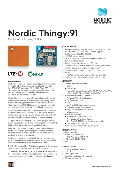
RGB LEDs
Temperature, humidity, air quality
and air pressure Light/color sensor
Buzzer
2.4 GHz antenna
Low-power accelerometer PMIC Battery connector Power switch
Nordic Thingy:91 Product Brief Verent Program/debug device
selection switch nRF9160 SiP
nRF52840 WLCSP
High-g accelerometer
Nano/4FF SIM card slot
An exhaustive set of sensors is included to gather data about the environment, and the movement of the Nordic Thingy:91. Temperature, humidity, air quality, air pressure, color and light data can easily be extracted for local or remote analysis.
and air pressure, plus a color and light sensor Low-power accelerometer and high-g accelerometer Buzzer 4 x N-MOS transistors for external DC motors or LEDs Rechargeable Li-Po battery with 1440 mAh capacity
AT89C5131A微控制器开发板用户指南说明书

AT89C5131A Starter Kit .............................................................................................. Hardware User GuideTable of ContentsSection 1Introduction...........................................................................................1-11.1Features....................................................................................................1-1Section 2Hardware Description...........................................................................2-32.1Block Diagram...........................................................................................2-32.2Power Supply............................................................................................2-42.3C51 Standard Settings..............................................................................2-52.4Feature Description...................................................................................2-62.5External Connectors.................................................................................2-8Section 3Device Programming............................................................................3-93.1In-System Programming...........................................................................3-93.2Using a Programmer.................................................................................3-9Section 4Appendix.............................................................................................4-114.1Electrical Schematics..............................................................................4-124.2Component Placement...........................................................................4-164.3Mechanical Outlines................................................................................4-174.4Bill of Materials........................................................................................4-17Section 1IntroductionThis document describes the AT89C5131A Starter Kit Evaluation Board dedicated tothe AT89C5131A USB microcontroller. This board is designed to allow an easy evalua-tion of the product using demonstration software (refer to Software Guide).1.1Features The AT89C5131A evaluation board provides the following features:Possibility to choose between two packages for the AT89C5131A–PLCC 52-pin package–VQFP 64-pin packageOn-board power supply circuitry–from an external power connector–from an external battery–from the USB line via the USB on-board connectorOn-board reset, INT0, LEDs, EA, ISP and programming interfacePower, ALE, RS232 Rx and Tx LEDsExternal system clock connectorPCA clock connectorUSB, TWI, SPI and RS232 hardware connectorsTwo Connectors available for extended boardIntroductionFigure 1-1. AT89C5131A Evaluation BoardHardware DescriptionSection 2Hardware Description2.1Block DiagramFigure 2-1. AT89C5131A Evaluation Board ComponentsAT89C5131APowerSupplyUSB TWISPIRS232LEDC51 Generic Board InterfaceResetISPEAINT0DeviceDeviceHost,Device...HumanC51 Generic BoardProgrammingSpecific DeviceInterfaceHardware Description2.2Power SupplyThe on-board power supply circuitry allows various power supply configurations.The power source can be:–V BUS from USB (5V)–V BUS from USB (5V) through the current limiter –External power supply (from 6 to 12V) or 9V batteryThe voltage output can be the direct power source, regulated at 5V or 3.3V.The power supply selection is performed using the JP2, JP3, JP4 and JP5 jumpers.The power supply can be turned on/off using the “power” switch (SW6). Once the power is established, the power LED (D9) is lit.Figure 2-2. Different Power ConfigurationsLIMREG V B U S5V 3.3V I C CPWR.S.PWRVCC LIMREG V B U S5V 3.3V I C CPWR.S.PWRVCC LIMREG V B U S5V 3.3V I C CPWR.S.PWR VCC LIM REGV B U S5V3.3V I C CPWR.S.PWRVCC LIMREGV B U S5V 3.3V I C CPWR.S.PWRVCC LIMREG V B U S5V 3.3V I C CPWR.S.PWRVCC LIM REGV B U S5V3.3V I C CPWR.S.PWRVCC LIMREGV B U S5V 3.3V I C CPWR.S.PWRVCC LIMREG V B U S5V 3.3V I C CPWR.S.PWRVCC VBUSVBUS and Current LimiterExternalDirect Input5V Regulate3.3V RegulatePower SourceRegulationHardware Description 2.3C51 StandardSettings2.3.1Reset The external Reset push-button (SW3) is provided to easily generate a warm reset. Thisbutton is used for ISP process. The Reset applied is active low.2.3.2Clock A crystal can be easily installed on the Y1 socket. The clock can also be provided usingthe J8 connector instead of the crystal.Note:Remove the clock generators before the using the programmer.2.3.3EA Place a jumper on the EA connector (J10) to force the EA pin to ground and executeexternal code. Otherwise internal code will be executed.Figure 2-3. EA Circuitry2.3.4INT0In order to use the on-board INT0 circuitry, connect the J7 Jumper to the AT89C5131A.When you press the INT0 button (SW5), the P3.2 pin will go low which induces an inter-rupt event.Note:Remove the J7 jumper before using the programmer. Otherwise the program-mer will not function.Figure 2-4. INT0 CircuitryHardware Description2.4FeatureDescription2.4.1RS232The AT89C5131A evaluation board includes all the required hardware to manage theRS232 communication.Figure 2-5. RS232 On-board Circuitry2.4.2USB Peripheral The AT89C5131A evaluation board provides all the required hardware to develop aUSB firmware for the AT89C5131A, this includes:–a USB connector–2 test points on D+ and D-–1 test point on V BUS–a USB UNLOAD button which allows to disconnect the pull-up on D+ and thento simulate an Attach/Detach of the USB cableThe USB peripheral can also be used to perform an In-System Programming.Hardware Description2.4.3TWI PeripheralThe CT3 and CT5 contacts have to be soldered in order to use the SDA and SCL alter-nate P4.1 and P4.0 port configuration on the SPI connector (J4).In order to use these signals on the J5 extension connector (SDA and SCL), the CT4and CT6 contacts have to also be soldered.2.4.4SPI Peripheral2.4.5LED Controller The AT89C5131A controller includes an LED controller on:–P3.3 (LED 0)–P3.5 (LED 1)–P3.6 (LED 2)–P3.7 (LED 3)The on board LEDs can be controlled with the AT89C5131A if the corresponding con-tacts CT9, CT10, CT11 and CT12 are bypassed.Figure 2-6. On-board LEDs for LED Controller1LED32CT9CT10CT11CT12LED 0LED 1LED 2LED 3Hardware Description2.5ExternalConnectorsThese two external connectors to build a customer extended board easily.Figure 2-7. Top View of J5 and J6 ConnectorsP1.0P1.1P1.2P1.3P1.4P1.5P1.6P1.7P3.0P3.1P3.2P3.3P3.4P3.5 P3.6 - WR P3.7 - RDNCNCNCNCNCNCNCNCVCCVSSSDASCLNCRESETEABP1A16NCVSSXTAL2VSSNCNCNCNCNCNCNCNCBUZZERVSSVSS4745434139373533312927252321191715131197531484644424038363432302826242220181614121086424.35 12V4.35 12VVSSNCNCNCNCNCNCNCNCPSENVSSALEP1.0 - KBD 0P1.1 - KBD 1P1.2 - KBD 2P1.3 - KBD 3P1.4 - KBD 4P1.5 - KBD 5P1.6 - KBD 6P1.7 - KBD 7VSSVSSP0.0P0.1P0.2P0.3P0.4P0.5P0.6P0.7P2.0P2.1P2.2P2.3P2.4P2.5P2.6P2.7P4.0P4.1NCNCNCNCNCNC474543413937353331292725232119171513119753148464442403836343230282624222018161412108642 J5J6AT89C5131A Starter Kit Hardware User Guide3-9Rev. 4245A–USB–11/04Section 3Device Programming3.1In-System ProgrammingThe user memory of the AT89C5131A part can be programmed using the ISP mode of the device. In order to enter in ISP mode, first select the high pin count mode (PSEN) or the low pin count mode (P1.0) using the ISP switch (SW2).To enter in ISP mode, press both the RESET (SW3) and ISP (SW4) buttons simulta-neously. First release the RESET button and then the ISP button. The device enters in ISP mode.ISP can then be performed using the USB bus (or with the peripheral corresponding with the bootloader version). The user may need to re-enumerate the USB bus using the USB UNLOAD button (SW1) if the USB cable is already connected.3.2Using aProgrammerThe AT89C5131A microcontroller can also be programmed using a programmer with the J3 connector. Connect all required signals between the programmer and the J3 con-nector and remove the J7 jumper to disconnect the EA circuitry. No clock should be enabled on the board, except the clock coming from the J3 connector.Figure 3-1. J3 Connector Schematic1VCC 2VSS 3XTAL14VSS 5NC 6RST7P3.2 (Test0)8VSS9P3.4 (Test1)10VSSJ3AT89C5131A Starter Kit Hardware User Guide4-11Rev. 4245A–USB–11/04Section 4Appendix4.14245A–USB–11/044245A–USB–11/04Appendix4245A–USB–11/04Appendix4245A–USB–11/04Appendix4245A–USB–11/04Appendix4245A–USB–11/044.2Component PlacementFigure 4-1. AT89C5131A Evaluation Board OverviewFigure 4-2. AT89C5131A Evaluation Board Component ImplementationAT89C5131A Evab 1.0.2J5J6Appendix4245A–USB–11/044.3Mechanical OutlinesFigure 4-3. AT89C5131A Evaluation Board Mechanical Outlines4.4Bill of MaterialsTable 4-1. Bill of MaterialsReference Part C11, C1222 pF C2 2.2 nF C1, C10, C1410 nF C9, C13100 nF C3, C4, C5, C6, C7, C8, C15, C17,C20, C210.1 µFC16, C1910 µF R4, R527R3100R15180R1, R6, R13, R191K R2 1.5K R10 2.2K R7, R8, R9 4.7K R11, R12, R1410KAppendix4245A–USB–11/04D2LED GREEN D1, D7, D9LEDs RED D3, D4, D5, D6LEDs PWR GREEND8MRA4007D11SMBJ9.0A U1MAX202ECSE U8DF005S TP1, TP2, TP3, TP4, TP5, TP6TEST POINTS J7, J10, J12JUMPERJ13CONNECTOR JACK PWR J8, J9CONNECTORS BNC P1SUB-D9 FEMALEJ1USB B J6, J5HEADER 24X2J11CONNECTOR SIP2J4CONNECTOR SIP4 RA J2CONNECTOR SIP6 RA J3CONNECTOR HE10SW2, SW6SW KEY-SPDT U3AT89C5131A_52U5AT89C5131A_VQFP64CT1, CT2, CT3, CT4, CT5, CT6, CT7, CT8, CT9, CT10, CT11, CT12, CT13,CT14CONTACTC1810 µF TANTALD101N4002JP1A16_Buzz Jumper JP2Limiter Jumper JP3Power Source Jumper JP4Regulator Jumper JP5V CC Level jumperR20121-1%R21365-1%R22196-1%SW1CONTACT BREAKERTable 4-1. Bill of Materials (Continued)ReferencePartAppendixTable 4-1. Bill of Materials (Continued)Reference PartSW3, SW4, SW5PUSH-BUTTONU2MAX708SCSAU6TPS2041ADU9LM1084/TO263Y1CRYSTAL4245A–USB–11/04Disclaimer: Atmel Corporation makes no warranty for the use of its products, other than those expressly contained in the Company’s standard warranty which is detailed in Atmel’s Terms and Conditions located on the Company’s web site. The Company assumes no responsibility for any errors which may appear in this document, reserves the right to change devices or specifications detailed herein at any time without notice, and does not make any commitment to update the information contained herein. No licenses to patents or other intellectual property of Atmel are granted by the Company in connection with the sale of Atmel products, expressly or by implication. Atmel’s products are not authorized for use as critical components in life support devices or systems.Atmel CorporationAtmel Operations2325 Orchard Parkway San Jose, CA 95131Tel: 1(408) 441-0311Fax: 1(408) 487-2600Regional HeadquartersEuropeAtmel SarlRoute des Arsenaux 41Case Postale 80CH-1705 Fribourg SwitzerlandTel: (41) 26-426-5555Fax: (41) 26-426-5500AsiaRoom 1219Chinachem Golden Plaza 77 Mody Road Tsimshatsui East Kowloon Hong KongTel: (852) 2721-9778Fax: (852) 2722-1369Japan9F, Tonetsu Shinkawa Bldg.1-24-8 ShinkawaChuo-ku, Tokyo 104-0033JapanTel: (81) 3-3523-3551Fax: (81) 3-3523-7581Memory2325 Orchard Parkway San Jose, CA 95131Tel: 1(408) 441-0311Fax: 1(408) 436-4314Microcontrollers2325 Orchard Parkway San Jose, CA 95131Tel: 1(408) 441-0311Fax: 1(408) 436-4314La Chantrerie BP 7060244306 Nantes Cedex 3, France Tel: (33) 2-40-18-18-18Fax: (33) 2-40-18-19-60ASIC/ASSP/Smart CardsZone Industrielle13106 Rousset Cedex, France Tel: (33) 4-42-53-60-00Fax: (33) 4-42-53-60-011150 East Cheyenne Mtn. Blvd.Colorado Springs, CO 80906Tel: 1(719) 576-3300Fax: 1(719) 540-1759Scottish Enterprise Technology Park Maxwell BuildingEast Kilbride G75 0QR, Scotland Tel: (44) 1355-803-000Fax: (44) 1355-242-743RF/AutomotiveTheresienstrasse 2Postfach 353574025 Heilbronn, Germany Tel: (49) 71-31-67-0Fax: (49) 71-31-67-23401150 East Cheyenne Mtn. Blvd.Colorado Springs, CO 80906Tel: 1(719) 576-3300Fax: 1(719) 540-1759Biometrics/Imaging/Hi-Rel MPU/High Speed Converters/RF DatacomAvenue de Rochepleine BP 12338521 Saint-Egreve Cedex, France Tel: (33) 4-76-58-30-00Fax: (33) 4-76-58-34-80e-mail********************Web Site4245A–USB–11/04/xM© Atmel Corporation 2004. All rights reserved. Atmel ® and combinations thereof are the registered trademarks of Atmel Corporation or its subsidiaries. Other terms and product names may be the trademarks of others.。
海信行输出高频头通用表
BSC29-N2409
回扫变压器
BSC29-N2416 BSC29-01B17
回扫变压器
BSC29-N2419
回扫变压器
BSC29-N2420A
回扫变压器
BSC29-N2423
回扫变压器
BSC29-N2424
回扫变压器
BSC29-N2425
回扫变压器
BSC29-N2426
回扫变压器
BSC29-N2429
010102B01017
A高频头
TDQ-3B9H-1,TDQ-3B9H-HP,TDC-3H3-5VL,TELE4-801A, ENV59D25G3,TDQ-3B9H-1SA,TELE4-871A,3B9H-116H,3B9H-2,IT-50YTLR,TDC-3H3-5DL,VTS-7ZH1,XG6SVD86B,IT-50YTLR
010102B04036
高频头
JS-5A/1216HS可代DTD11D01
010102B04037
高频头
UV3116CS,UV3116CSA,TDC-3H3-HT,UV3116VC
010102B04047
高频头HDP3411
DTD19DM011通JS-5A/1236HS
010202B02020
高频头
010101A08072
行输出
BSC29-0146A /0101-83833
010101A08076
行输出HDP2908
JF0101-83836通BSC20-0115D
010101A08078
行输出TC2977
JF0101-85915通29--N2426/A
010101A08080
行输出HDP3411
SMB1351 高通模块原厂规格书

描述
接地 系统用电输出(3.0V-4.5V),最大支持4.5A电流 外置MosFet驱动脚 电池充电输出脚 OTG/ID检测 模拟电压输出,指示USB输入端实时充电电流值 Suspend控制管脚 电池温度检测输入端 DCIN检测,当插入USB时,PGOOD输出2.5V高电平 充电使能,模块内部已接下拉电阻到GND,已开启使能 USB9/5/1.5/HC选择,内部已接下拉电阻到GND 状态输出 电源检测,接到USB D+/DIIC通信接口 辅助电源输出,最小50mA 电源输入脚,接到USB VBUS
PGOOD SMB1351-EJ3
BAT+ BAT-
24 GND 23 SY SON 22 MID 21 USB+ 20 USB+ 19 SCL 18 SDA 17
D+ 16 D- 15 STAT 14 USBCS 13 EN
图 1: 移动电源应用电路
J1 1 2 VBUS 3 D4 D+ 5 GND
Rev 1.0 12
EJRQC3003 模块说明书
{
SET_SDAT_OUT; wait();
SCLK(0);
SDA(0);
wait();
SCLK(1);
wait();
SDA(1);
}
void _i2c_no_ack(void)
{
SET_SDAT_OUT; wait();
SCLK(0);
wait();
#define WriteADDR
0xAE
#define ReadADDR
0xAF
#define BaterryNotFULL 0
#define BaterryFULL 1
各种无线传输模块

无线模块选型指南名称:无线模块选型指南NRF905/NRF24L01/CC1100/Si4432/CC1020/CC2500...型号:各型号综合介绍“物联网”概念风起云涌,无线应用大行其道。
如在选型阶段就正确确定最适合要求的型号,无疑能缩短开发周期,尽快实现无线应用。
本栏目旨在简要概括介绍各无线模块的性能特点,给您的无线选型提供初步参考“物联网”概念风起云涌,无线应用大行其道,如无线监控、无线抄表、无线点菜、传感网络、无线称重等领域。
以无线替代有线,是个必然的发展趋势。
在此情况下,作为无线应用厂商,应考虑如何快速地推出符合市场需求的无线应用产品,抢占市场的蓝海。
作为专业的无线模块设计及供应商,飞拓电子专注于无线通信领域的开发及应用,能提供齐全的无线基础性产品(无线模块),专业的开发指导,大大减少您公司产品的开发周期。
本栏目旨在简要概括介绍各无线模块的性能特点,给您的无线选型提供初步参考。
Si4432模块性能及特点:(1) 完整的FSK收发器(2) 工作频率433M免费ISM频段(430.24~439.75MHz),也可以工作于900.72~929.27MHz(3) 最大发射功率17dBm(4) 接收灵敏度高达-115 dBm(5) 传输速率最大128Kbps(6) FSK频偏可编程(15~240KHz)(7) 接收带宽可编程(67~400KHz)(8) SPI兼容的控制接口,低功耗任务周期模式,自带唤醒定时器(9) 低的接收电流(18.5mA),最大发射功率时的电流:73mA (10)空旷通讯距离可达800米以上(波特率9.6Kbps)RF903模块性能及特点:(1) 433MHz 开放ISM 频段免许可证使用(2) 最高工作速率50kbps,高效GFSK调制,抗干扰能力强,特别适合工业控制场合(3) 125 频道,满足多点通信和跳频通信需要(4) 内置硬件CRC 检错和点对多点通信地址控制(5) 低功耗3-3.6V 工作,待机模式下状态仅为2.5uA,TX Mode在+10dBm情况下,电流为40mA; RX Mode为14mA(6) 收发模式切换时间 < 650us(7) 模块可软件设地址,只有收到本机地址时才会输出数据(提供中断指示),可直接接各种单片机使用,软件编程非常方便(8) 增加了电源切断模式,可以实现硬件冷启动功能!(9) SPI接口—功能强大、编程简单,与RF905SE编程接口类似。