bq24020官方图纸
(完整版)手机结构设计手册(内部资料)
手机结构手设计手册目录赛微电子网整理第1章绪论 (4)1.1 手机的分类 (4)1.2 手机的主要结构件名称 (5)1.3 手机结构件的几大种类 (5)1.4 手机零件命名规则 (5)1.5 手机结构设计流程 (11)第2章手机壳体的设计和制造工艺 (12)2.1 前言 (12)2.2 手机常用材料 (12)2.2.1 PC(学名聚碳酸酯) (12)2.2.2 ABS(丙烯腈-丁二烯-苯乙烯共聚物) (13)2.2.3 PC+ABS(PC与ABS的合成材料) (13)2.2.4 选材要点 (13)2.3 手机壳体的涂装工艺 (14)2.3.1 涂料 (14)2.3.2 喷涂方法 (15)2.3.3 涂层厚度 (15)2.3.4 颜色及光亮度 (15)2.3.5 色板签样 (15)2.3.6 耐磨及抗剥离检测 (15)2.3.7 涂料生产厂家 (16)2.4 手机壳体的模具加工 (16)2.5 塑胶件加工要求 (16)2.5.1 尺寸,精度及表面粗糙度的要求 (16)2.5.2 脱模斜度的要求 (17)2.5.3 壁厚的要求 (17)2.5.4 加强筋 (17)2.5.5 圆角 (18)2.6 手机3D设计 (18)2.6.1 手机3D建模思路 (18)2.6.2 手机结构设计 (19)第3章按键的设计及制造工艺 (26)3.1 前言 (26)- I -赛微电子网整理- -II 3.2 P +R 按键设计与制造工艺 (26)3.3 硅胶按键设计与制造工艺 (27)3.4 PC (IMD )按键设计与制造工艺 (28)3.5 Metal Dome 的设计 (28)3.5.1 概述 (28)3.5.2 Metal Dome 的设计 (29)3.5.3 Metal Dome 触点不同表面镀层性能对比 (29)3.5.4 Metal Dome 技术特性 (29)3.6 手机按键设计要点 (30)第4章 标牌和镜片设计及其制造工艺 (33)4.1 前言 (33)4.2 金属标牌设计与制造工艺 (33)4.2.1 电铸Ni 标牌制造工艺 (33)4.2.2 铝合金标牌制造工艺 (35)4.3 塑料标牌及镜片设计与制造工艺 (36)4.3.1 IMD 工艺 (36)4.3.2 IML 工艺 (38)4.3.3 IMD 与IML 工艺特点比较 (39)4.3.4 注塑镜片工艺 (39)4.3.5 IMD 、IML 、注塑工艺之比较 (42)4.4 平板镜片设计与制造工艺 (42)4.4.1 视窗玻璃镜片 (42)4.4.2 塑料板材镜片 (42)4.5 镀膜工艺介绍 (43)4.5.1 真空镀 (43)4.5.2 电镀 俗称水镀 (44)4.5.3 喷镀 (44)第5章 金属部件设计及制造工艺 (45)5.1 前言 (45)5.2 镁合金成型工艺 (45)5.2.1 镁合金压铸工艺 (45)5.3 金属屏蔽盖设计与制造工艺 (46)5.3.1 屏蔽盖材料 (46)手机结构手设计手册目录赛微电子网整理5.3.2 设计要求 (46)5.4 弹片设计要点 (47)5.4.1 冷轧碳素钢弹片 (47)5.4.2 不锈钢弹片 (47)5.4.3 磷青铜弹片 (47)5.4.4 铍青铜弹片 (47)5.5 螺钉、螺母及弹簧设计要点 (48)5.5.1 螺钉 (48)5.5.2 热压螺母 (48)5.5.3 弹簧 (49)第6章手机结构设计相关测试标准 (51)6.1 环境条件试验方法 (51)6.1.1 低温试验 (51)6.1.2 高温试验 (51)6.1.3 潮热试验 (52)6.1.4 温度冲击试验 (52)6.1.5 振动试验 (52)6.1.6 跌落试验 (53)6.1.7 盐雾试验 (53)6.2 涂层耐磨和抗剥离检测 (54)6.2.1 耐磨检测 (54)6.2.2 涂层附着力检测——抗剥离检测 (55)6.2.3 设计和检测注意事项 (55)6.3 拟订的J耐磨检测方案 (55)6.3.1 涂层耐磨检测(第一方案) (55)6.3.2 涂层耐磨检测(第二方案) (56)6.3.3 涂层附着力检测 (56)- III -赛微电子网整理- - IV第1章 绪论1.1 手机的分类随着国内通信业的迅猛发展,国内手机行业的竞争也日趋白热化,国内外各手机厂商纷纷推出不同样式、功能的手机。
mini2440原理图

nOE nWAIT
nWE OM0 OM1
LADDR0 LADDR1 LADDR2 LADDR3 LADDR4 LADDR5 LADDR6 LADDR7 LADDR8 LADDR9 LADDR10 LADDR11 LADDR12 LADDR13 LADDR14 LADDR15 LADDR16 LADDR17 LADDR18 LADDR19 LADDR20 LADDR21 LADDR22 LADDR23 LADDR24 LADDR25
L3 nXDACK0 K7 nLED_3 K6 nXDREQ0 K5 nLED_4
R35 4.7K U1A
CON5
C5
XTIpll
15p X2
12M
C6
XTOpll
15p
nXDACK0/GPB9 nXDACK1/GPB7 nXDREQ0/GPB10 nXDREQ1/GPB8
nXBACK/GPB5 nXBREQ/GPB6
NAND CTRL
nFCEGPA22
nFRE/GPA20
nFWE/GPA19
SDCLK/GPE5 SSDDCDMATDA/G0/PGEP6E7SDIO SDDATA1/GPE8 SDDATA2/GPE9 SDDATA3/GPE10
UART
VD0/GPC8
USS
VD1/GPC9 VD2/GPC10
VD3/GPC11
22p
XTIrtc
C1 X1
32.768kHz
XTOrtc
C2 22p
C B
AIN0 AIN1 AIN2 AIN3 AIN4/TSYM AIN5/TSYP AIN6/TSXM AIN7/TSXP Aref EXYCLK CLKOUT0/GPH9 CLKOUT1/GPH10 MPLLCAP UPLLCAP OM2 OM3 XTIpll XTOpll XTIrtc XTOrtc TOUT0/GPB0 TOUT1/GPB1 TOUT2/GPB2 TOUT3/GPB3 TCLK0/GPB4 TCLK1/EINT19/GPG11
湖南省院CAD 制图标准

湖南省建筑设计院CAD 制图标准湖南省建筑设计院CAD 制图标准(2011-02-23 起执行)湖南省建筑设计院湖南省建筑设计院CAD 制图标准目录1、总则 (5)1.1 目的 (5)1.2 制定依据 (5)1.3 适用范围 (5)2、文件管理 (6)2.1 文件格式 (6)2.1.1 图形文件 (6)2.1.2 图像文件 (6)2.1.3 文本文件 (6)2.1.4 其它文件 (6)2.2 文件类型 (6)2.2.1 数据文件 (6)2.2.2 页面文件 (6)2.3 文件命名规则 (6)2.4 图纸管理 (8)2.4.1 图纸排序 (8)2.4.2 图纸编号 (8)2.4.3 封面 (8)2.4.4 图纸目录 (8)2.4.5 规格格式 (9)2.5 图纸规格 (9)2.5.1 图幅尺寸 (9)2.5.2 出图比例 (10)2.5.3 模版文件 (10)2.6 图纸模板 (11)2.6.1 施工图封面 (11)2.6.2 图纸目录 (13)2.6.3 图框样本 (15)2.6.4 标准图签 (16)2.6.5 标准图纸模板的取用: (18)湖南省建筑设计院CAD 制图标准3、二维制图 (181)3.1 比例 (18)3.1.1 图样的比例 (18)3.1.2 比例标识 (18)3.1.3 比例规定 (18)3.1.4 自选比例 (18)3.2 字体 (18)3.2.1 图面文字 (18)3.2.2 字体 (19)3.2.3 间距 (19)3.2.4 缺省值 (19)3.2.5 汉字 (19)3.2.6 字体字高 (19)3.3 图线 (19)3.3.1 线宽 (19)3.3.2 线宽组 (19)3.3.3 基本图线名称 (20)3.3.4 图框线宽 (20)3.4 轴线 (20)3.5 符号 (22)3.6 尺寸标注和标记 (23)3.7 其他 (24)4、专业制图 (252)4.1 专业图层规则 (25)4.2 专业图例、大样规则 (25)4.3 建筑专业 (26)4.4 结构专业 (30)4.5 给排水专业 (35)4.6 采暖通风空气调节专业 (40)湖南省建筑设计院CAD 制图标准4.7 电气专业 (43)二维协同CAD 标准湖南省建筑设计院CAD 制图标准本标准规定了建筑计算机辅助设计(以下简称CAD)过程中制图统一规则,主要包括定义、二维制图、专业制图和文件交换格式等。
某3层砖混结构加固改造全套结构施工图(3套)

预埋件图集(最终版).

U
U
U
U
I.总 说 明
I. 总 说 明
1 适用范围 1.1 本图集适用于火力发电厂建筑物中的混凝土、钢筋混凝土和
预应力混凝土结构。 1.2 在下列情形下必须根据现行专门规范、规程和技术规定的要
求重新验算。 1.2.1 用于轻骨料混凝土结构时。 1.2.2 处于侵蚀环境中的结构。 1.2.3 表面温度高于摄氏 100 度时。 1.2.4 承受振动荷载需作振动计算时。 1.3 不适用于混凝土厚度小于 50mm 的薄壁构件和截面宽度小于
TU
UT
TU
UT
IX. 与吊车梁翼缘连接的柱面预埋件.................................................................................................................................... 40
fy
+
M
1.3α aα bα r
fyz
(6)
As
≥
M 0.4α aαbα r
fyz
(7)
3.2.6 受斜拉预埋件(柱间支撑用预埋件,参见图—5),按下列两 个公式计算并取ABsB的较大值:
As
≥
N fy
⎜⎜⎝⎛
cosϕ α rαv
+ sinϕ 0.8α aαb
+
e0 1.3α
sin ϕ aα bα
r
式中 V —剪力设计值; M —弯矩设计值, M = V ⋅ e0 ; α a ,αb ,α r ,αv —各符号意义同以上各式。
S
且 且
0
V
V
创维20xxxTV系列图纸

R46 47R
R47 47R
1 2 3 4
1 2 3 4
MIV2571-2B
R811 10K
C812 103
10K R802 R804 10K T1 T2 T3 T4 T5
U801 BT BM1 SCL SDA AS
470U
470U
R814 4.7K
C802 4.7U
+5V
C813 1U
R702A 47R
D 5-8
G S 4 U38 1-3 IRF7805
D8 L101 C321 C322 C323
C324 C99 C100
U18 1-3 5-8 D IRF7404 G PWR-CNTL S
ADD U4V for DPTV 3D 1 3 U40 5 FAN2500S25 For DPTV PLL RAMDAC Power A
+5V输 出 3 U34 2 AS1117 For PP135 Digital Power
ht
tp :
1
ht tp : // zg j dw x. 5d 中 6 国 d. 家 co 电 m 维 /b 修 b 论 s. 坛 ph
p
辉 达
电
子
辉 达
1 2 3 4 5 6
dw x. 5d 中 6 国 d. 家 co 电 m 维 /b 修 b 论 s. 坛 ph
zg j
S
D 5-8 1-3 U37 IRF7807 4 G
4 D 1-3 U21 5-8 IRF7404
HS
For Intervor
10
13 U4 74LS04
PTV-PWR-CNTL
U19 3 LT1084 2
丙类单层车间厂房建筑设计施工图
2#BT转炉本体电气非标订货图纸

BQ24020(中文)

1锂离子电池充电过程锂系列(锂离子或锂聚合物)电池的充电过程分为3个阶段,如图1所示。
图1三阶段充电流程图第一阶段为检验和预充电阶段。
该阶段主要的任务是:验证电池的温度并将其调整到适合快速充电的范围内;检测电池电压并将其提高到一个安全水平。
温度检验和预充电提高了电池的安全性和使用寿命。
第二阶段将以“1C”或略低的电流进行恒流充电。
一旦电池达到它的电压限幅4.1V或4.2V,则已完成对大约70%的容量的充电,并进入第三阶段充电。
第三阶段是对电池进行恒压充电,为了使安全性和电量达到最大化,需要将充电电压稳定在±1%的精度内。
在恒压充电阶段,充电电流逐渐变小,并且在大多数情况下,当这个充电电流接近快速充电电流的10%,即C/10时,充电过程就结束了。
2基于bqTINY-II的电源管理模块bqTINY-II是TI推出的电池充电管理芯片,它为电源系统设计人员带来一套集成解决方案。
该芯片将自动电源选择、功率FET和电流传感器、高精准度的稳流和稳压能力、充电状态显示和充电中止等功能集为一体。
它的一个重要特点是其可以选择两种充电模式,支持目前流行的USB接口充电。
bqTINY-II支持三阶段的充电程序如图1所示,包括预充电调节阶段、恒流充电阶段以及许多设备制造商都要求的高精准度恒压充电阶段。
bqTINY-II的功耗极低,当系统未连接至电源时,bqTINY-II就会进入低功耗休眠模式,它此时只会从电池汲取非常少的电量。
2.1示意电路图该方案的示意电路如图2所示,该原理图以bq24020芯片为核心,配以必要的外围元器件。
由于bq24020芯片的高集成化,使得所需的外围元器件大大减小,只需要3颗滤波电容和1颗用于设置AC预充率的电阻即可。
图2bq24020的电源管理示意图图2所示电源管理模块有4个输入接口,4个输出接口和一个公共地。
其中4个输入接口为:交流适配器AC接口、USB取电接口、充电使能信号CE、USB充电点设置;4个输出接口为:电源输出、电源温度信号输出、2个充电状态指示输出。
BQ24080中文资料

FEATURES DESCRIPTIONAPPLICATIONSADAPTERbq24080SLUS698B–MARCH2006–REVISED MAY2006 SINGLE-CHIP,LI-ION AND LI-POL CHARGER IC•Small3mm×3mm MLP Package The bq24080is a highly integrated and flexible Li-Ionlinear charge device targeted at space-limited •Integrated Power FET and Current Sensor forcharger applications.It offers an integrated power Up to1-A Charge Applications From ACFET and current sensor,high-accuracy current and Adaptervoltage regulation,charge status,and charge •Precharge Conditioning With Safety Timer termination,in a single monolithic device.An external•Charge and Power Good(AC Adapter Present resistor sets the magnitude of the charge current.With Fixed Safety)Status OutputThe bq24080charges the battery in three phases:•Automatic Sleep Mode for Low-Power conditioning,constant current,and constant voltage.Consumption Charge is terminated based on minimum current.Aninternal charge timer provides a backup safety for •Fixed7-Hour Fast Charge Safety Timercharge termination.The bq24080automatically •Ideal for Low-Dropout Charger Designs forrestarts the charge if the battery voltage falls below Single-Cell Li-Ion or Li-Pol Packs in an internal threshold.The bq24080automaticallySpace-Limited Portable Applications enters sleep mode when the input supply isremoved.•PDAs,MP3Players•Digital Cameras•Internet Appliances•SmartphonesPlease be aware that an important notice concerning availability,standard warranty,and use in critical applications of TexasInstruments semiconductor products and disclaimers thereto appears at the end of this data sheet.PowerPAD is a trademark of Texas Instruments.PRODUCTION DATA information is current as of publication date.Copyright©2006,Texas Instruments Incorporated Products conform to specifications per the terms of the TexasInstruments standard warranty.Production processing does notnecessarily include testing of all parameters.DISSIPATION RATINGSABSOLUTE MAXIMUM RATINGSRECOMMENDED OPERATING CONDITIONSbq24080SLUS698B–MARCH 2006–REVISED MAY 2006These devices have limited built-in ESD protection.The leads should be shorted together or the device placed in conductive foam during storage or handling to prevent electrostatic damage to the MOS gates.ORDERING INFORMATIONCHARGE FAST-CHARGE TIMERPART T JREGULATION FUNCTIONSMARKINGS(HOURS)NUMBER (1)(2)VOLTAGE (V)bq24080DRCR -40°C to 125°C 4.2CE and PG 7BRObq24080DRCT(1)The DRC package is available taped and reeled only in quantities of 3,000devices per reel.(2)For the most current package and ordering information,see the Package Option Addendum at the end of this document,or see the TI Web site at .T A <40°C DERATING FACTOR PACKAGE θJA θJC POWER RATINGABOVE T A =25°CDRC (1)46.87°C/W4.95°C/W1.5W0.021W/°C(1)This data is based on using the JEDEC High-K board and the exposed die pad is connected to a copper pad on the board.This is connected to the ground plane by a 2x 3via matrix.over operating free-air temperature range unless otherwise noted (1)bq24080UNIT V IInput voltage (2)IN,CE,ISET,OUT,PG,STAT1,STAT2-0.3to 7V Output sink/source current STAT1,STAT2,PG 15mA Output currentOUT1.5A T A Operating free-air temperature range°C -40to 125T J Junction temperature range °C T stg Storage temperature–65to 150°CLead temperature 1,6mm (1/16inch)from case for 10seconds300(1)Stresses beyond those listed under absolute maximum ratings may cause permanent damage to the device.These are stress ratings only,and functional operation of the device at these or any other conditions beyond those indicated under recommended operating conditions is not implied.Exposure to absolute-maximum-rated conditions for extended periods may affect device reliability.(2)All voltages are with respect to V SS .MINMAX UNIT V CC Supply voltage4.5 6.5V T JOperating junction temperature range125°C2Submit Documentation FeedbackELECTRICAL CHARACTERISTICSbq24080 SLUS698B–MARCH2006–REVISED MAY2006over0°C≤TJ≤125°C and recommended supply voltage(unless otherwise noted)PARAMETER TEST CONDITIONS MIN TYP MAX UNITINPUT CURRENTI CC(VCC)V CC current V CC>V CC(min) 1.22mASum of currents into OUT pin,I CC(SLP)Sleep current25V CC<V(SLP)I CC(STBY)Standby current CE=High,0°C≤T J≤85°C150µAI IB(OUT)Input current on OUT pin Charge DONE,V CC>V CC(MIN)15I IB(CE)Input current on CE pin CE=High1VOLTAGE REGULATION V O(REG)+V(DO–MAX)≤V CC,I(TERM)<I O(OUT)≤1AV O(REG)Output voltage 4.2VT A=25°C–0.35%0.35% Voltage regulation accuracy–1%1%V O(OUT)=V O(REG),I O(OUT)=1AV(DO)Dropout voltage(V(IN)–V(OUT))350500mVV O(REG)+V(DO))≤V CCCURRENT REGULATIONV I(OUT)>V(LOWV),I O(OUT)Output current range(1)V I(IN)–V I(OUT)>V(DO),501000mAV CC≥4.5VVoltage on ISET pin,V CC≥4.5V,V(SET)Output current set voltage V I≥4.5V,V I(OUT)>V(LOWV), 2.463 2.5 2.538VV I–V I(OUT)>V(DO)50mA≤I O(OUT)≤1A307322337K(SET)Output current set factor10mA≤I O(OUT)<50mA2963203461mA≤I O(OUT)<10mA246320416PRECHARGE AND SHORT-CIRCUIT CURRENT REGULATIONPrecharge to fast-charge transitionV(LOWV)Voltage on OUT pin 2.83 3.2V thresholdV CC(MIN)≥4.5V,t FALL=100ns,Deglitch time for fast-charge to10-mV overdrive,250375500ms precharge transitionV I(OUT)decreasing below thresholdI O(PRECHG)Precharge range(2)0V<V I(OUT)<V(LOWV),t<t(PRECHG)5100mAVoltage on ISET pin,V(PRECHG)Precharge set voltage V O(REG)=4.2V,240255270mV0V<V I(OUT)>V(LOWV),t<t(PRECHG)TERMINATION DETECTIONCharge termination detectionI(TERM)V I(OUT)>V(RCH),t<t(TRMDET)5100mA range(3)Voltage on ISET pin,Charge termination detection setV(TERM)V O(REG)=4.2V,235250265mV voltageV I(OUT)>V(RCH),t<t(TRMDET)V CC(MIN)≥4.5V,t FALL=100nsDeglitch time for terminationt TRMDET charging current decreasing below250375500ms detection10-mV overdrive(1)See Equation2in the Function Description section.(2)See Equation1in the Function Description section.(3)See Equation3in the Function Description section.3Submit Documentation Feedbackbq24080SLUS698B–MARCH 2006–REVISED MAY 2006ELECTRICAL CHARACTERISTICS (continued)over 0°C ≤T J ≤125°C and recommended supply voltage (unless otherwise noted)PARAMETERTEST CONDITIONSMINTYPMAXUNITBATTERY RECHARGE THRESHOLD V O(REG)–V O(REG)–V O(REG)–V (RCH)Recharge thresholdV 0.1150.100.085V CC(MIN)≥4.5V,t FALL =100ns t (DEGL)Deglitch time for recharge detectdecreasing below or increasing 250375500msabove threshold,10-mV overdrive STAT1,STAT2,and PG OUTPUTS V OL Low-level output saturation voltage I O =5mA 0.25VCHARGE ENABLE (CE),INPUTSV IL Low-level input voltage I IL =10µA 00.4V V IH High-level input voltage I IL =20µA1.4I IL CE,low-level input current -1µAI IH CE,high-level input current1TIMERS t (PRECHG)Precharge time 1,6201,8001,930s t (CHG)Charge time22,68025,20027,720s I (FAULT)Timer fault recovery current200µASLEEP COMPARATOR V CC ≤V I(OUT)V (SLP)Sleep-mode entry threshold voltage+80mV2.3V ≤V I(OUT)≤V O(REG)VV CC ≥V I(OUT)V (SLPEXIT)Sleep-mode exit threshold voltage +190V (IN)decreasing below threshold,Sleep-mode deglitch time250375500mst FALL =100ns,10-mV overdriveTHERMAL SHUTDOWN ENTRY THRESHOLDS T (SHTDWN)Thermal trip threshold 165T J increasing°CThermal hysteresis15UNDERVOLTAGE LOCKOUT V (UVLO)Undervoltage lockout Decreasing V CC2.42.5 2.6V Hysteresis27mV4Submit Documentation FeedbackPIN ASSIGNMENTbq24080 SLUS698B–MARCH2006–REVISED MAY2006DRC PACKAGE(TOP VIEW)TERMINAL FUNCTIONSTERMINALI/O DESCRIPTIONNAME NO.IN1I Adapter dc voltageCE9I Charge enable input(active low voltage,min0.1µF input capacitor)GND2,7-GroundISET6I Charge current.Precharge and termination set point.OUT10O Charge current output(minimum0.1µF capacitor to ground)PG8O Power-good status output(open-drain)STAT13O Charge status output1(open-drain)STAT24O Charge status output2(open-drain)VSS5-GroundThere is an internal electrical connection between the exposed thermal pad and VSS pin of the device.The Thermal exposed thermal pad must be connected to the same potential as the VSS pin on the printed-circuit board.Do --Pad not use the thermal pad as the primary ground input for the device.VSS pin must be connected toground at all times.5Submit Documentation FeedbackINGNDCEbq24080SLUS698B–MARCH 2006–REVISED MAY 2006FUNCTIONAL BLOCK DIAGRAM6Submit Documentation Feedback10005015050300200350250400450100150T J - Junction T emperature -CoD r o p o u t V o l t a g e - m VPreœConditioningRegulationV oltage RegulationCurrentMinimumCharge V oltagePre-Conditioningand T erm DetectUDG-04087bq24080SLUS698B–MARCH 2006–REVISED MAY 2006DROPOUT VOLTAGEvsFigure 1.The bq24080supports a precision Li-Ion,Li-Pol charging system suitable for single cells.Figure 2shows a typical charge profile,and Figure 3shows an operational flow chart.Figure 2.Typical Charging Profile7Submit Documentation FeedbackFUNCTIONAL DESCRIPTIONbq24080SLUS698B–MARCH 2006–REVISED MAY 2006Figure 3.Operational Flow Chart8Submit Documentation FeedbackBattery PreconditioningIO(PRECHG)=K(SET)(PRECHG)x VRSET(1)Battery Fast Charge Constant CurrentI= O(OUT)K V(SET)(SET)xRSET(2)Battery Fast Charge Voltage Regulation Charge Termination Detection and RescueIO(TERM)=K V(SET)(TERM)xRSET(3)bq24080SLUS698B–MARCH2006–REVISED MAY2006 FUNCTIONAL DESCRIPTION(continued)During a charge cycle if the battery voltage is below the V(LOWV)threshold,the bq24080applies a precharge current,I O(PRECHG),to the battery.This feature revives deeply discharged cells.The resistor connected between the ISET and V SS,R SET determines the precharge rate.The V(PRECHG)and K(SET)parameters are specified in the specifications table.The bq24080activates a safety timer,t(PRECHG),during the conditioning phase.If the V(LOWV)threshold is not reached within the timer period,the bq24080turns off the charger and enunciates FAULT on the STATx pins. See the Timer Fault Recovery section for additional details.The bq24080offers on-chip current regulation with programmable set point.The resistor connected between the ISET and V SS,R SET determines the charge rate.The V(SET)and K(SET)parameters are specified in the specifications table.The voltage regulation feedback is through the OUT pin.This input is tied directly to the positive side of the battery pack.The bq24080monitors the battery-pack voltage between the OUT and VSS pins.When the battery voltage rises to V O(REG)threshold,the voltage regulation phase begins and the charging current begins to taper down.As a safety backup,the bq24080also monitors the charge time in the charge mode.If charge is not terminated within this time period,t(CHG),the charger is turned off and FAULT is set on the STATx pins.See the Timer Fault Recovery section for additional details.The bq24080monitors the charging current during the voltage regulation phase.Once the termination threshold, I(TERM),is detected,charge is terminated.The V(TERM)and K(SET)parameters are specified in the specifications table.After charge termination,the bq24080restarts the charge once the voltage on the OUT pin falls below the V(RCH) threshold.This feature keeps the battery at full capacity at all times.The bq24080monitors the charging current during the voltage regulation phase.Once the termination threshold, I(TERM),is detected,the charge is terminated immediately.The resistor connected between the ISET and V SS,R SET determines the current level at the termination threshold.9Submit Documentation FeedbackSleep ModeChange Status OutputsPG OutputCE Input (Charge Enabled)bq24080SLUS698B–MARCH 2006–REVISED MAY 2006FUNCTIONAL DESCRIPTION (continued)The bq24080enters the low-power sleep mode if the input power (IN)is removed from the circuit.This feature prevents draining the battery during the absence of input supply.The open-drain STAT1and STAT2outputs indicate various charger operations as shown in the following table.These status pins can be used to drive LEDs or communicate to the host processor.Note that OFF indicates the open-drain transistor is turned off.Table 1.Status Pin SummaryCHANGE STATE STAT1STAT2Precharge in progress ON ON Fast charge in progressON OFF Charge doneOFFONCharge suspend (temperature)Timer fault OFFOFFSleep modeThe open-drain PG (Power Good)output pulls low when a valid input voltage is present.This output is turned off,(high impedance)sleep mode.The PG pin can be used to drive an LED or communicate to the host processor.The CE digital input is used to disable or enable the charge process.A low-level signal on this pin enables the charge and a high-level signal disables the charge and places the device in a low-power mode.A high-to-low transition on this pin also resets all timers and timer fault conditions.10Submit Documentation FeedbackTimer Fault RecoveryCondition Number1Condition number2Selecting Input and Output Capacitorsbq24080 SLUS698B–MARCH2006–REVISED MAY2006As shown in Figure3,bq24080provides a recovery method to deal with timer fault conditions.The following summarizes this method:OUT pin voltage is above the recharge threshold(V(RCH)),and a timeout fault occurs.Recovery method:bq24080waits for the OUT pin voltage to fall below the recharge threshold.This could happen as a result of a load on the battery,self-discharge,or battery removal.Once the OUT pin voltage falls below the recharge threshold,the bq24080clears the fault and starts a new charge cycle.A POR or CE toggle also clears the fault.OUT pin voltage is below the recharge threshold(V(RCH)),and a timeout fault occursRecovery method:Under this scenario,the bq24080applies the I(FAULT)current.This small current is used to detect a battery removal condition and remains on as long as the battery voltage stays below the recharge threshold.If the OUT pin voltage goes above the recharge threshold,then the bq24080disables the I(FAULT) current and executes the recovery method described for condition number1.Once the OUT pin voltage falls below the recharge threshold,the bq24080clears the fault and starts a new charge cycle.A POR or CE toggle also clears the fault.In most applications,all that is needed is a high-frequency decoupling capacitor on the input power pin.A0.1-µF ceramic capacitor,placed in close proximity to the IN pin and GND pad works well.In some applications,it may be necessary to protect against a hot plug input voltage overshoot.This is done in three ways:1.The best way is to add an input zener,6.2V,between the IN pin and VSS.2.A low power zener is adequate for the single event transient.Increasing the input capacitance lowers thecharacteristic impedance which makes the input resistance move effective at damping the overshoot,but risks damaging the input contacts by the high inrush current.3.Placing a resistor in series with the input dampens the overshoot,but causes excess power dissipation.The bq24080only requires a small capacitor for loop stability.A0.1-µF ceramic capacitor placed between the OUT and GND pad is typically sufficient.Figure4.Typical Application Circuit11Submit Documentation FeedbackAPPLICATION INFORMATIONThermal Considerationsq JA =T -T J A P (4)P = (V - V ) x I (IN)(OUT)O(OUT)(5)PCB Layout Considerationsbq24080SLUS698B–MARCH 2006–REVISED MAY 2006The bq24080is packaged in a thermally enhanced MLP package.The package includes a thermal pad to provide an effective thermal contact between the device and the printed-circuit board (PCB).Full PCB design guidelines for this package are provided in the application note entitled,QFN/SON PCB Attachment (TI Literature Number SLUA271).The most common measure of package thermal performance is thermal impedance (θJA )measured (or modeled)from the device junction to the air surrounding the package surface (ambient).The mathematical expression for θJA is:Where:•T J =device junction temperature•T A =ambient temperature•P =device power dissipationFactors that can greatly influence the measurement and calculation of θJA include:•Orientation of the device (horizontal or vertical)•Volume of the ambient air surrounding the device under test and airflow•Whether other surfaces are in close proximity to the device being tested•Use multiple 10-13mil vias in the PowerPAD™to copper ground plane.•Avoid cutting the ground plane with a signal trace near the power IC.•The PCB must be sized to have adequate surface area for heat dissipation.•FR4(figerglass)thickness should be minimized.The device power dissipation,P,is a function of the charge rate and the voltage drop across the internal Power FET.It can be calculated from the following equation:Due to the charge profile of Li-xx batteries,the maximum power dissipation is typically seen at the beginning of the charge cycle when the battery voltage is at its lowest.See Figure 2.It is important to pay special attention to the PCB layout.The following provides some guidelines:•To obtain optimal performance,the decoupling capacitor from V CC to V (IN)and the output filter capacitorsfrom OUT to VSS should be placed as close as possible to the bq24080,with short trace runs to both signal and VSS pins.The VSS pin should have short trace runs to the GND pin.•All low-current V SS connections should be kept separate from the high-current charge or discharge pathsfrom the e a single-point ground technique incorporating both the small-signal ground path and the power ground path.•The high-current charge paths into IN and from the OUT pins must be sized appropriately for the maximum charge current in order to avoid voltage drops in these traces.•The bq24080is packaged in a thermally enhanced MLP package.The package includes a thermal pad to provide an effective thermal contact between the device and the printed circuit board (PCB).Full PCBdesign guidelines for this package are provided in the application note entitled,QFN/SON PCB Attachment (TI Literature Number SLUA271).12Submit Documentation FeedbackIMPORTANT NOTICETexas Instruments Incorporated and its subsidiaries (TI) reserve the right to make corrections, modifications, enhancements, improvements, and other changes to its products and services at any time and to discontinue any product or service without notice. Customers should obtain the latest relevant information before placing orders and should verify that such information is current and complete. All products are sold subject to TI’s terms and conditions of sale supplied at the time of order acknowledgment.TI warrants performance of its hardware products to the specifications applicable at the time of sale in accordance with TI’s standard warranty. Testing and other quality control techniques are used to the extent TI deems necessary to support this warranty. Except where mandated by government requirements, testing of all parameters of each product is not necessarily performed.TI assumes no liability for applications assistance or customer product design. Customers are responsible for their products and applications using TI components. To minimize the risks associated with customer products and applications, customers should provide adequate design and operating safeguards.TI does not warrant or represent that any license, either express or implied, is granted under any TI patent right, copyright, mask work right, or other TI intellectual property right relating to any combination, machine, or process in which TI products or services are used. Information published by TI regarding third-party products or services does not constitute a license from TI to use such products or services or a warranty or endorsement thereof. Use of such information may require a license from a third party under the patents or other intellectual property of the third party, or a license from TI under the patents or other intellectual property of TI. Reproduction of information in TI data books or data sheets is permissible only if reproduction is without alteration and is accompanied by all associated warranties, conditions, limitations, and notices. Reproduction of this information with alteration is an unfair and deceptive business practice. TI is not responsible or liable for such altered documentation.Resale of TI products or services with statements different from or beyond the parameters stated by TI for that product or service voids all express and any implied warranties for the associated TI product or service and is an unfair and deceptive business practice. TI is not responsible or liable for any such statements. Following are URLs where you can obtain information on other Texas Instruments products and application solutions:Products ApplicationsAmplifiers Audio /audioData Converters Automotive /automotiveDSP Broadband /broadband Interface Digital Control /digitalcontrolLogic Military /militaryPower Mgmt Optical Networking /opticalnetwork Microcontrollers Security /securityTelephony /telephonyVideo & Imaging /videoWireless /wirelessMailing Address:Texas InstrumentsPost Office Box 655303 Dallas, Texas 75265Copyright 2006, Texas Instruments Incorporated。
笔记本电池数据解密工具使用说明
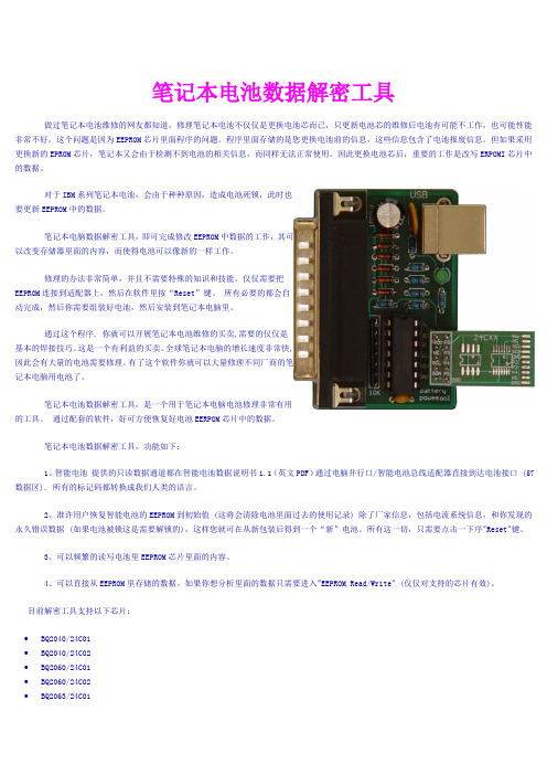
笔记本电池数据解密工具做过笔记本电池维修的网友都知道,修理笔记本电池不仅仅是更换电池芯而已,只更新电池芯的维修后电池有可能不工作,也可能性能非常不好。
这个问题是因为EEPROM芯片里面程序的问题。
程序里面存储的是您更换电池前的信息,这些信息包含了电池报废信息。
但如果采用更换新的EPROM芯片,笔记本又会由于检测不到电池的相关信息,而同样无法正常使用。
因此更换电池芯后,重要的工作是改写ERPOMI芯片中的数据。
对于IBM系列笔记本电池,会由于种种原因,造成电池死锁,此时也要更新EEPROM中的数据。
笔记本电脑数据解密工具,即可完成修改EEPROM中数据的工作,其可以改变存储器里面的内容,而使得电池可以像新的一样工作。
修理的办法非常简单,并且不需要特殊的知识和技能。
仅仅需要把EEPROM连接到适配器上,然后在软件里按“Reset”键。
所有必要的都会自动完成,然后你需要组装好电池,然后安装到笔记本电脑里。
通过这个程序, 你就可以开展笔记本电池维修的买卖,需要的仅仅是基本的焊接技巧。
这是一个有利益的买卖。
全球笔记本电脑的增长速度非常快,因此会有大量的电池需要修理。
有了这个软件你就可以大量修理不同厂商的笔记本电脑用电池了。
笔记本电池数据解密工具,是一个用于笔记本电脑电池修理非常有用的工具。
通过配套的软件,好可方便恢复好电池EERPOM芯片中的数据。
笔记本电池数据解密工具,功能如下:1、智能电池提供的只读数据通道都在智能电池数据说明书1.1(英文PDF)通过电脑并行口/智能电池总线适配器直接到达电池接口 (57 数据区). 所有的标记码都转换成我们人类的语言。
2、准许用户恢复智能电池的EEPROM到初始值 (这将会清除电池里面过去的使用记录) 除了厂家信息,包括电流系统信息,和你发现的永久错误数据 (如果电池被锁这是需要解锁的),这样您就可在从新包装后得到一个“新”电池。
所有这一切,只需要点击一下序"Reset"键。
20层办公楼电气设计施工图纸

某地小学小型锅炉房建筑设计施工图

西安神电三相组合式避雷器
7.5 7.2
13.5 13.5
11.5 11.5
YH5WZ1-10/27×10/27 YH5WZ1-17/45×17/45 YH5WZ-32/90×32/85
6 10
10
8.0
相-相 15.0 相-地 14.4
27.0 27.0
17
13.6
相-相 相-地
25.0 24.0
45.0 45.0
23.0
e. 长期施加在避雷器端子间的工频电压应不超过避雷器的持续运行电
压(无间隙型)或额定电压(带串联间隙型);
f. 地震烈度 8 度及以下地区;
g. 最大风速不超过 35m/s;
h. 重污秽及以下地区。
异常运行条件,请在合同中注明。
四、主要技术参数
本产品依据其结构特征分为无间隙和有串联间隙两大类,具体型号及主
一、概述
三相组合式复合外套金属氧化物避雷器在对相地之间的过电压提供保护
的同时,又对相间过电压提供保护。本产品结构新颖,外形组合灵活多变,
有效的利用和缩减了使用空间。技术性能合理可靠,保护水平满足 GB11032
《交流无间隙金属氧化物避雷器》、JB/T 10496《交流三相组合式无间隙金属
氧化物避雷器》、JB/T 10609《交流三相组合式有串联间隙金属氧化物避雷器》、
10.5* 13.5
11.5
相-相 相-地
23.2 18.6
38.0 31.0
31.0 用 25.0
注: 1. 配电用、电动机用操作冲击电流为 100A;电站用、发电机用操作冲击电流为 250A; 并联补偿电容器用操作冲击电流为 500A。
2. 带*参数表示电机额定电压。
3
表 2 三相组合式复合外套有串联间隙金属氧化物避雷器
- 1、下载文档前请自行甄别文档内容的完整性,平台不提供额外的编辑、内容补充、找答案等附加服务。
- 2、"仅部分预览"的文档,不可在线预览部分如存在完整性等问题,可反馈申请退款(可完整预览的文档不适用该条件!)。
- 3、如文档侵犯您的权益,请联系客服反馈,我们会尽快为您处理(人工客服工作时间:9:00-18:30)。
bq24020EVM and bq24023EVM
1-A Single-Chip Li-Ion and Li-Pol Charge Management IC with Autonomous USB-Port and AC-Adapter Supply Management Evaluation Module
Mailing Address: Texas Instruments Post Office Box 655303 Dallas, Texas 75265
Copyright 2003, Texas Instruments Incorporated
2
DYNAMIC WARNINGS AND RESTRICTIONS It is important to operate this EVM within the input voltage range of VREG + 0.5 to 5.2 V and the output range of 0 V to 4.2 V. Exceeding the specified input range may cause unexpected operation and/or irreversible damage to the EVM. If there are questions concerning the input range, please contact a TI field representative prior to connecting the input power. Applying loads outside of the specified output range may result in unintended operation and/or possible permanent damage to the EVM. Please consult the EVM User’s Guide prior to connecting any load to the EVM output. If there is uncertainty as to the load specification, please contact a TI field representative. During normal operation, some circuit components may have case temperatures greater than 70°C. The EVM is designed to operate properly with certain components above 70°C as long as the input and output ranges are maintained. These components include but are not limited to linear regulators, switching transistors, pass transistors, and current sense resistors. These types of devices can be identified using the EVM schematic located in the EVM User ’s Guide. When placing measurement probes near these devices during operation, please be aware that these devices may be very warm to the touch. Mailing Address: Texas Instruments Post Office Box 655303 Dallas, Texas 75265
User’s Guide
1
EVM IMPORTANT NOTICE Texas Instruments (TI) provides the enclosed product(s) under the following conditions: This evaluation kit being sold by TI is intended for use for ENGINEERING DEVELOPMENT OR EVALUATION PURPOSES ONLY and is not considered by TI to be fit for commercial use. As such, the goods being provided may not be complete in terms of required design-, marketing-, and/or manufacturing-related protective considerations, including product safety measures typically found in the end product incorporating the goods. As a prototype, this product does not fall within the scope of the European Union directive on electromagnetic compatibility and therefore may not meet the technical requirements of the directive. Should this evaluation kit not meet the specifications indicated in the EVM User’s Guide, the kit may be returned within 30 days from the date of delivery for a full refund. THE FOREGOING WARRANTY IS THE EXCLUSIVE WARRANTY MADE BY SELLER TO BUYER AND IS IN LIEU OF ALL OTHER WARRANTIES, EXPRESSED, IMPLIED, OR STATUTORY, INCLUDING ANY WARRANTY OF MERCHANTABILITY OR FITNESS FOR ANY PARTICULAR PURPOSE. The user assumes all responsibility and liability for proper and safe handling of the goods. Further, the user indemnifies TI from all claims arising from the handling or use of the goods. Please be aware that the products received may not be regulatory compliant or agency certified (FCC, UL, CE, etc.). Due to the open construction of the product, it is the user’s responsibility to take any and all appropriate precautions with regard to electrostatic discharge. EXCEPT TO THE EXTENT OF THE INDEMNITY SET FORTH ABOVE, NEITHER PARTY SHALL BE LIABLE TO THE OTHER FOR ANY INDIRECT, SPECIAL, INCIDENTAL, OR CONSEQUENTIAL DAMAGES. TI currently deals with a variety of customers for products, and therefore our arrangement with the user is not exclusive. TI assumes no liability for applications assistance, customer product design, software performance, or infringement of patents or services described herein. Please read the EVM User’s Guide and, specifically, the EVM Warnings and Restrictions notice in the EVM User’s Guide prior to handling the product. This notice contains important safety information about temperatures and voltages. For further safety concerns, please contact the TI application engineer. Persons handling the product must have electronics training and observe good laboratory practice standards. No license is granted under any patent right or other intellectual property right of TI covering or relating to any machine, process, or combination in which such TI products or services might be or are used.
