SOT143-00-C002-GC中文资料
LM143中文资料
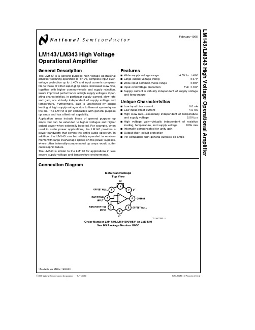
Electrical Characteristics (Note 3)
Parameter Input Offset Voltage Input Offset Current Input Bias Current Supply Voltage Rejection Ratio Output Voltage Swing Large Signal Voltage Gain Common-Mode Rejection Ratio Input Voltage Range Supply Current (Note 5) Short Circuit Current Slew Rate Power Bandwidth Unity Gain Frequency Input Offset Voltage Input Offset Current Input Bias Current Large Signal Voltage Gain Output Voltage Swing Conditions Min TA e 25 C TA e 25 C TA e 25 C TA e 25 C TA e 25 C RL t 5 kX TA e 25 C VOUT e g 10V RL t 100 kX TA e 25 C TA e 25 C TA e 25 C TA e 25 C TA e 25 C AV e 1 TA e 25 C VOUT e 40 Vp-p RL e 5 kX THD s 1% TA e 25 C TA e Max TA e Min TA e Max TA e Min TA e Max TA e Min RL t 100 kX TA e Max RL t 100 kX TA e Min RL t 5 0 kX TA e Max RL t 5 0 kX TA e Min 50k 50k 22 22 08 18 50 16 150k 220k 26 25 22 100k 80
BYV143X-45中文资料

Philips Semiconductors Product specificationRectifier diodes BYV143F, BYV143X seriesSchottky barrierFEATURESSYMBOLQUICK REFERENCE DATA• Low forward volt drop • Fast switching• Reverse surge capability• High thermal cycling performance • Isolated packageGENERAL DESCRIPTIONDual,common cathode schottky rectifier diodes in a plastic envelope with electrically isolated mounting tab.Intended for use as output rectifiers in low voltage,high frequency switched mode power supplies.The BYV143F series is supplied in the SOT186package.The BYV143X series is supplied in the SOT186A package.PINNINGSOT186SOT186APIN DESCRIPTION 1anode 1 (a)2cathode (k)3anode 2 (a)tabisolatedLIMITING VALUESLimiting values in accordance with the Absolute Maximum System (IEC 134)SYMBOL PARAMETERCONDITIONSMIN.MAX.UNITBYV143F-354045BYV143X-354045V RRM Peak repetitive reverse -354045V voltageV RWM Working peak reverse -354045V voltageV R Continuous reverse voltage T hs ≤ 82 ˚C-354045V I O(AV)Average rectified output square wave; δ = 0.5;-20A current (both diodes T hs ≤ 83 ˚Cconducting)I FRM Repetitive peak forward square wave; δ = 0.5;-20A current per diodeT hs ≤ 83 ˚C I FSMNon-repetitive peak forward t = 10 ms -100A current per diode t = 8.3 ms-110A sinusoidal; T j = 125 ˚C prior to surge; with reapplied V RRM(max)I RRM Peak repetitive reverse pulse width and repetition rate -1A surge current per diode limited by T j maxT j Operating junction -150˚C temperatureT stgStorage temperature- 65175˚C123case123casePhilips Semiconductors Product specification Rectifier diodes BYV143F, BYV143X series Schottky barrierISOLATION LIMITING VALUE & CHARACTERISTICThs= 25 ˚C unless otherwise specifiedSYMBOL PARAMETER CONDITIONS MIN.TYP.MAX.UNITVisol Peak isolation voltage from SOT186 package; R.H. ≤ 65%; clean and--1500V all terminals to external dustfreeheatsinkVisol R.M.S. isolation voltage from SOT186A package; f = 50-60 Hz;--2500V all terminals to external sinusoidal waveform; R.H. ≤ 65%; cleanheatsink and dustfreeCisol Capacitance from pin 2 to f = 1 MHz-10-pF external heatsinkTHERMAL RESISTANCESSYMBOL PARAMETER CONDITIONS MIN.TYP.MAX.UNITRth j-hs Thermal resistance junction per diode-- 5.7K/W to heatsink both diodes-- 4.8K/W(with heatsink compound)Rth j-a Thermal resistance junction in free air-55-K/W to ambientELECTRICAL CHARACTERISTICSTj= 25 ˚C unless otherwise specifiedSYMBOL PARAMETER CONDITIONS MIN.TYP.MAX.UNITVF Forward voltage IF= 15 A; Tj= 125˚C-0.550.62VIF= 20 A-0.650.8VI R Reverse current VR= VRWM-0.12 1.5mAVR= VRWM; Tj= 100˚C-1530mACd Junction capacitance VR= 5 V; f = 1 MHz, Tj= 25˚C to 125˚C-450-pFPhilips Semiconductors Product specificationRectifier diodes BYV143F, BYV143X seriesSchottky barrierPhilips Semiconductors Product specificationRectifier diodes BYV143F, BYV143X seriesSchottky barrierMECHANICAL DATANotes1. Refer to mounting instructions for F-pack envelopes.2. Epoxy meets UL94 V0 at 1/8".Philips Semiconductors Product specificationRectifier diodes BYV143F, BYV143X seriesSchottky barrierMECHANICAL DATA1. Refer to mounting instructions for F-pack envelopes.2. Epoxy meets UL94 V0 at 1/8".Philips Semiconductors Product specification Rectifier diodes BYV143F, BYV143X series Schottky barrierDEFINITIONSData sheet statusObjective specification This data sheet contains target or goal specifications for product development. Preliminary specification This data sheet contains preliminary data; supplementary data may be published later. Product specification This data sheet contains final product specifications.Limiting valuesLimiting values are given in accordance with the Absolute Maximum Rating System (IEC 134). Stress above one or more of the limiting values may cause permanent damage to the device. These are stress ratings only and operation of the device at these or at any other conditions above those given in the Characteristics sections ofthis specification is not implied. Exposure to limiting values for extended periods may affect device reliability. Application informationWhere application information is given, it is advisory and does not form part of the specification.© Philips Electronics N.V. 1998All rights are reserved. Reproduction in whole or in part is prohibited without the prior written consent of the copyright owner.The information presented in this document does not form part of any quotation or contract, it is believed to be accurate and reliable and may be changed without notice. No liability will be accepted by the publisher for any consequence of its use. Publication thereof does not convey nor imply any license under patent or other industrial or intellectual property rights.LIFE SUPPORT APPLICATIONSThese products are not designed for use in life support appliances, devices or systems where malfunction of these products can be reasonably expected to result in personal injury. Philips customers using or selling these products for use in such applications do so at their own risk and agree to fully indemnify Philips for any damages resulting from such improper use or sale.。
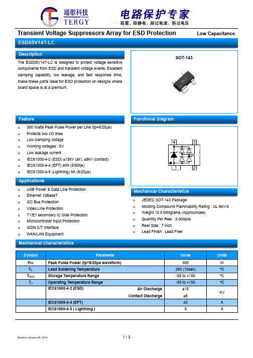
静电保护器SOT-143封装参数型号规格书大全
Revision January 06, 2014
1/3
Transient Voltage Suppressors Array for ESD Protection
ESD05V14T-LC
Low Capacitance
Electrical Characteristics (@ 25℃ Unless Otherwise Specified )
θ
0°
-
8° 0° - 8°
aaa
0.006
0.15
bbb
0.008
0.20
ccc
0.004
0.10
Soldering Footprint
Symbol C E1 E2 G X1 X2 Y Z
Inches (0.087) 0.076 0.068 0.031 0.039 0.047 0.055 0.141
t - Time (μs)
Fig3. Power Derating Curve
% of Rated Power
110 100
90 80 70
60 50 40 30 20
10 0 0
25
50
75 100 125 150
Ambient Temperature – TA (ºC)
Fig2. ESD Pulse Waveform (according to IEC 61000-4-2)
Millimeters (2.20) 1.92 1.72 0.80 1.00 1.20 1.40 3.60
Revision January 06, 2014
3/3
100% 90%
Percent of Peak Pulse Current %
OCM143中文资料
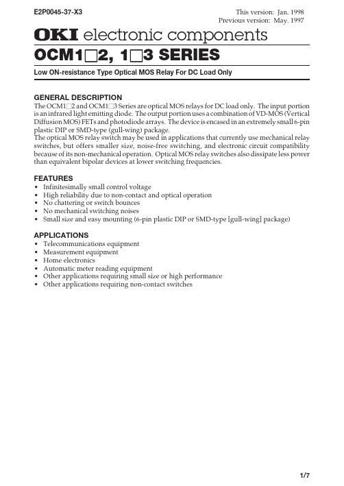
OCM1M 2, 1M 3 SERIESLow ON-resistance Type Optical MOS Relay For DC Load OnlyGENERAL DESCRIPTIONThe OCM1M 2 and OCM1M 3 Series are optical MOS relays for DC load only. The input portion is an infrared light emitting diode. The output portion uses a combination of VD-MOS (Vertical Diffusion MOS) FETs and photodiode arrays. The device is encased in an extremely small 6-pin plastic DIP or SMD-type (gull-wing) package.The optical MOS relay switch may be used in applications that currently use mechanical relay switches, but offers smaller size, noise-free switching, and electronic circuit compatibility because of its non-mechanical operation. Optical MOS relay switches also dissipate less power than equivalent bipolar devices at lower switching frequencies.FEATURES•Infinitesimally small control voltage•High reliability due to non-contact and optical operation •No chattering or switch bounces •No mechanical switching noises•Small size and easy mounting (6-pin plastic DIP or SMD-type [gull-wing] package)APPLICATIONS•Telecommunications equipment •Measurement equipment •Home electronics•Automatic meter reading equipment•Other applications requiring small size or high performance •Other applications requiring non-contact switchesE2P0045-37-X3This version: Jan. 1998Previous version: May. 1997元器件交易网PIN CONFIGURATION(Unit: mm)• DIP Type• SMD Type (gull-wing)• Pin Connection Diagram1: Anode2: Cathode 3: NC 4: Drain 5: Source 6: Source(LED)(LED)(MOS FET)(MOS FET)(MOS FET)• Through hole (Bottom view)• Mounting pad (Top view)+15-00°+15-00°8.682.54 5.081.26.4± 0.55.68±0.255.93±0.25±0.2±0.10.5±0.2±0.37.62±0.150.25±0.033.65±0.24.75M A X0.8±0.22.8±0.35yrqe5.088.68±0.51.2±0.22.54±0.10.5±0.26.4±0.33.65±0.24.0±0.20.25±0.031.1±0.41.1±0.49.9±0.6yrq eABSOLUTE MAXIMUM RATINGSProduct NameParameterSymbolCondition Unit OCM102OCM103I n p u t C h a r a c t e r i s t i c sDerating Factor of Continuous Forward Current I F Pulse width 100 m s Cycle 10 msPulse width 1 ms 1shot(Ambient temperature Ta=25°C )OCM112OCM113OCM122OCM123OCM142OCM143Continuous Forward Current Peak Forward Current Reverse Voltage Power Dissipation Load Voltage Load Current Derating Factor of Load Current Surge Load Current Power Dissipation Storage TemperatureOperating Temperature Isolation Voltage Total Power DissipationO u t p u t C h a r a c t e r i s t i c sD I F I FM V R P DL V OFF I ON D I ON I SUG P D P totV IO T opr T stgmA mA/°CA V mW V mA mA/°C A mW mWV(rms)°C °C50Refer to [Derating Factor of Continuous Forward Current] of characteristics data0.55200350Refer to [Derating Factor of Load Current] of characteristics data3.53003251500OCM1224000OCM123–40 to +85–40 to +100400200OCM142OCM143100450OCM112OCM11360500OCM102OCM103751.5ELECTRICAL CHARACTERISTICSProduct NameParameterSymbolCondition Unit OCM102OCM103I n p u t C h a r a c t e r i s t i c sReverse CurrentV F V OFF =50 V f=1 MHz (Ambient temperature Ta=25°C )OCM112OCM113OCM122OCM123OCM142OCM143Forward Voltage Recovery Input CurrentOn-resistance Off-state Leakage Current Output Terminal Capacitance O u t p u t C h a r a c t e r i s t i c sI RI FRR ONI OFF C OUT Min.m A mAW mA pF 1.0100.21.01.03.00.30.225Max.I F =10 mA V V R =5 V Max. 1.3Operation Input Current I FA mA 5I ON =100 mA Max.V OFF =Rating I ON =100 m A Min.*1Min. 1.5 4.50.70.5Typ. 2.06.21.00.75Max.I F =10 mA I ON =100 mATime to flow current is within one second*2V OFF =Rating Max.Typ.355070Input-to-output Capacitance C IO pF 1.3f=1 MHz Typ.t ON Turn-on Time Typ.0.3Max.I F =10 mA I ON =100 mAms 1.0t OFFTurn-off TimeTyp.0.2Max.ms1.0C o u p l i n g C h a r a c t e r i s t i c s *3*3*1 : Can correspond to special specification I FA <3.0 mA *2 : Can correspond to special specification I OFF <1.0 nA*3 : Can correspond to special specification t ON / t OFF <0.5 msTYPICAL CHARACTERISTICS•Derating Factor of Continuous Forward Current•Derating Factor of Load Current•Operation Input Current vs.Ambient Temperature•Recovery Input Current vs.Ambient Temperature•On-resistance vs. Ambient Temperature 1•On-resistance vs. Ambient Temperature 20–400501003010204050–0.5 mA/°CTemperature Ta (°C )C o n t i n u o u s F o r w a r d C u r r e n t I F (m A )600–40050100300100200400500Temperature Ta (°C )C o n t i n u o u s L o a d C u r r e n t I O N (m A )600–40050100Temperature Ta (˚C )O p e r a t i o n I n p u t C u r r e n t I F A (m A )–40050100Temperature Ta (°C )R e c o v e r y I n p u t C u r r en t I F R (m A )–40050100Temperature Ta (°C )O n -r e s i s t a n c e R O N (W )0050100102468Temperature Ta (°C)O n -r e s i s t a n c e R O N (W )–40•Turn-on/Turn-off Time vs.Ambient Temperature•Off-state Leakage Current vs.Ambient Temperature•Continuous Forward Current vs.On-resistance 1•Continuous Forward Current vs.Turn-on/Turn-off Time•Output Terminal Capacitance vs.Applied Voltage•Continuous Forward Current vs.On-resistance 2–400501000.010.110.001Temperature Ta (°C )T u r n -o n / T u r n -o f f T i m e (m s )050100Temperature Ta (°C )–4000512341020Input Current I F (mA)O n -r e s i s t a n c e R O N (W )001024681020Input Current I F (mA)O n -r e s i s t a n c e R O N (W )1100.2Input Current I F (mA)T u r n -o n / T u r n -o f f T i m e (m s )10100Applied Voltage (V)1010011O u t p u t T e r m i n a l C a p a c i t a n c e C o u t (p F )1000•Load Current vs. Voltage•Example Circuit for Measuring Turn-on/Turn-off TimeI FV OUTV OUT5000.20.40.60.81.0400300200100Voltage (V )L o a d C u r r e n t I O N (m A )。
贴片印字

DTA144EKA PZM16NB BZV49-C16 BAS125-07 BAS125-07W PDTC124ET PDTC124EU BFP181T PDTC143ZK PDTC143ZT PDTC143ZT PZM18NB BZV49-C18 PDTA143ZK DTA115EUA DTA115EKA PDTA143ZT PDTA143ZT SSTPAD100 PZM10NB1 PZM10NB2 PZM10NB3 PZM11NB1 DTA113ZUA PZM11NB2 PZM11NB3 DTA143ZUA PZM12NB1 DTC113ZUA PZM12NB2 PZM12NB3 DTC143ZUA PZM13NB1 PZM13NB2 DTA123JUA PZM13NB3 DTA123JUA PZM15NB1 PZM15NB2 PZM15NB3 DTA144VUA PZM16NB1 PZM16NB2 PZM16NB3 DTC144VUA
N C O S S N N X N N N C O N N N N N J C C C C N C C N C N C C N C C N C N C C C N C C C N
SC59 SOT346 SOT89 SOT143 SOT343 SOT23 SOT323 SOT346 SOT23 SOT23 SOT346 SOT89 SOT346 SC70 SC59 SOT23 SOT23 SOT23 SOT346 SOT346 SOT346 SOT346 SC70 SOT346 SOT346 SC70 SOT346 SC70 SOT346 SOT346 SC70 SOT346 SOT346 SC70 SOT346 SC70 SOT346 SOT346 SOT346 SC70 SOT346 SOT346 SOT346 SC70
MCCSEMI DTC143ECA 23 SOT-23 数字NPN传输器数据手册说明书

Counterfeiting of semiconductor parts is a growing problem in the industry. Micro Commercial Components (MCC) is taking strong measures to protect ourselves and our customers from the proliferation of counterfeit parts. MCC strongly encourages customers to purchase MCC parts either directly from MCC or from Authorized MCC Distributors who are listed by country on our web page cited below. Products customers buy either from MCC directly or from Authorized MCC Distributors are genuine parts, have full traceability, meet MCC's quality standards for handling and storage. MCC will not provide any warranty coverage or other assistance for parts bought from Unauthorized Sources. MCC is committed to combat this global problem and encourage our customers to do their part in stopping this practice by buying direct or from authorized distributors.
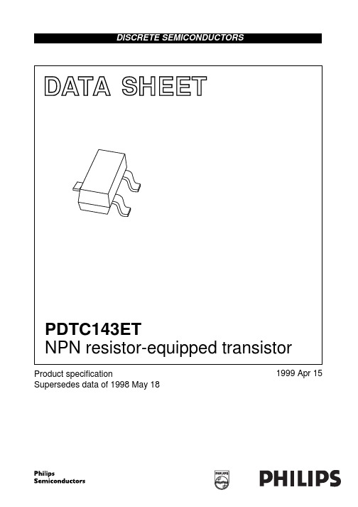
PDTC143ET中文资料
1.2
IE = ie = 0; VCB = 10 V; f = 1 MHz −
−
2.5 pF
1999 Apr 15
3
元器件交易网
Philips Semiconductors
NPN resistor-equipped transistor
Product specification
1999 Apr 15
4
元器件交易网
Philips Semiconductors
NPN resistor-equipped transistor
PACKAGE OUTLINE Plastic surface mounted package; 3 leads
Product specification
open emitter open base open collector
Tamb ≤ 25 °C; note 1
Note 1. Transistor mounted on an FR4 printed-circuit board.
MIN.
− − −
MAX. 50 50 10
UNIT V V V
−
30
• Inverter circuit configurations without use of external resistors.
DESCRIPTION
NPN resistor-equipped transistor in a SOT23 plastic package. PNP complement: PDTA143ET.
Fig.3 DC current gain as a function of collector current; typical values.
SOT143-00-C002-KG中文资料
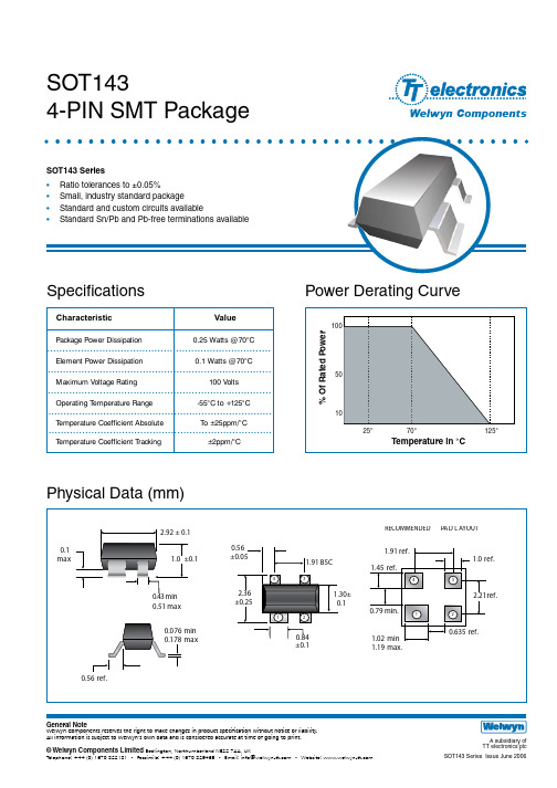
R1 (W) 500.0 10.0K 900.0 500.0 200.0
R2 (W) 50.0K 10.0K 100.0 48.0K 40.0K
R1 (W) 10.0K 900.0 1.0K
R2 (W) 10.0K 100.0 10.0K
R3 (W) 10.0K 9.0K 10.0K
Welwyn Components reserves the right to make changes in product specification without notice or liability. All information is subject to Welwyn’s own data and is considered accurate at time of going to print.
© Welwyn Components Limited Bedlington, Northumberland NE22 7AA, UK
A subsidiary of TT electronics plc SOT143 Series Issue June 2006
Telephone: +44 (0) 1670 822181 • Facsimile: +44 (0) 1670 829465 • Email: info@ • Website:
% Of Rated Power
50
10
25°
70°
125°
Temperature in °C
Physical Data (mm)
2.92 ± 0.1 0.1 max 1.0 ±0.1 0.56 ±0.05
4
SOT143中文资料

Welwyn Components reserves the right to make changes in product specification without notice or liability. All information is subject to Welwyn’s own data and is considered accurate at time of going to print.
..................................................................................................................................................... ..................................................................................................................................................... ..................................................................................................................................................... ..................................................................................................................................................... ..................................................................................................................................................... ..................................................................................................................................................... ..................................................................................................................................................... .....................................................................................................................................................
onsemi DTC143ZD D 双NPN偏置电阻晶体管 4.7kΩ,47kΩ 数据表说明书
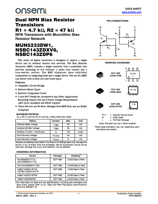
DATA SHEET Dual NPN Bias ResistorTransistorsR1 = 4.7 k W, R2 = 47 k WNPN Transistors with Monolithic BiasResistor NetworkMUN5233DW1,NSBC143ZDXV6,NSBC143ZDP6This series of digital transistors is designed to replace a singledevice and its external resistor bias network. The Bias ResistorTransistor (BRT) contains a single transistor with a monolithic biasnetwork consisting of two resistors; a series base resistor and abase-emitter resistor. The BRT eliminates these individual components by integrating them into a single device. The use of a BRT can reduce both system cost and board space.Features•Simplifies Circuit Design•Reduces Board Space•Reduces Component Count•S and NSV Prefix for Automotive and Other Applications Requiring Unique Site and Control Change Requirements;AEC-Q101 Qualified and PPAP Capable•These Devices are Pb-Free, Halogen Free/BFR Free and are RoHS CompliantMAXIMUM RATINGS(T A = 25°C, common for Q1 and Q2, unless otherwise noted)Rating Symbol Max UnitCollector-Base Voltage V CBO50Vdc Collector-Emitter Voltage V CEO50Vdc Collector Current − Continuous I C100mAdc Input Forward Voltage V IN(fwd)30Vdc Input Reverse Voltage V IN(rev)5Vdc Stresses exceeding those listed in the Maximum Ratings table may damage the device. If any of these limits are exceeded, device functionality should not be assumed, damage may occur and reliability may be affected. ORDERING INFORMATIONDevice Package Shipping†MUN5233DW1T1G,SMUN5233DW1T1GSOT−3633,000/T ape & Reel NSVMUN5233DW1T3G SOT−36310,000/T ape & ReelNSBC143ZDXV6T1G,NSVBC143ZDXV6T1GSOT−5634,000/T ape & Reel NSBC143ZDXV6T5G SOT−5638,000/Tape & Reel NSBC143ZDP6T5G SOT−9638,000/T ape & Reel †For information on tape and reel specifications, including part orientation andtape sizes, please refer to our Tape and Reel Packaging SpecificationsMARKING DIAGRAMSPIN CONNECTIONS7K/Y=Specific Device CodeM=Date Code*G=Pb-Free Package(Note: Microdot may be in either location)*Date Code orientation may vary depending upon manufacturing location.SOT−363CASE 419BSOT−563CASE 463A(1)(2)(3)SOT−963CASE 527ADY M17K M GG167K M G1THERMAL CHARACTERISTICSCharacteristic Symbol Max Unit MUN5233DW1 (SOT−363) ONE JUNCTION HEATEDTotal Device DissipationT A = 25°C(Note1)(Note2)Derate above 25°C(Note1)(Note2)P D1872561.52.0mWmW/°CThermal Resistance,(Note1) Junction to Ambient(Note2)R q JA670490°C/WMUN5233DW1 (SOT−363) BOTH JUNCTION HEATED (Note3)Total Device DissipationT A = 25°C(Note1)(Note2)Derate above 25°C(Note1)(Note2)P D2503852.03.0mWmW/°CThermal Resistance,Junction to Ambient(Note1)(Note2)R q JA493325°C/WThermal Resistance, Junction to Lead(Note1)(Note2)R q JL188208°C/WJunction and Storage Temperature Range T J, T stg−55 to +150°C NSBC143ZDXV6 (SOT−563) ONE JUNCTION HEATEDTotal Device DissipationT A = 25°C(Note1)Derate above 25°C(Note1)P D3572.9mWmW/°CThermal Resistance,Junction to Ambient(Note1)R q JA350°C/WNSBC143ZDXV6 (SOT−563) BOTH JUNCTION HEATED (Note3)Total Device DissipationT A = 25°C(Note1)Derate above 25°C(Note1)P D5004.0mWmW/°CThermal Resistance,Junction to Ambient(Note1)R q JA250°C/WJunction and Storage Temperature Range T J, T stg−55 to +150°C NSBC143ZDP6 (SOT−963) ONE JUNCTION HEATEDTotal Device DissipationT A = 25°C(Note4)(Note5)Derate above 25°C(Note4)(Note5)P D2312691.92.2MWmW/°CThermal Resistance,Junction to Ambient(Note4)(Note5)R q JA540464°C/WNSBC143ZDP6 (SOT−963) BOTH JUNCTION HEATED (Note3)Total Device DissipationT A = 25°C(Note4)(Note5)Derate above 25°C(Note4)(Note5)P D3394082.73.3MWmW/°CThermal Resistance,Junction to Ambient(Note4)(Note5)R q JA369306°C/WJunction and Storage Temperature Range T J, T stg−55 to +150°C 1.FR−4 @ Minimum Pad.2.FR−4 @ 1.0×1.0 Inch Pad.3.Both junction heated values assume total power is sum of two equally powered channels.4.FR−4 @ 100mm2, 1 oz. copper traces, still air.5.FR−4 @ 500mm2, 1 oz. copper traces, still air.ELECTRICAL CHARACTERISTICS (T A =25°C, common for Q 1 and Q 2, unless otherwise noted)CharacteristicSymbolMinTypMaxUnitOFF CHARACTERISTICS Collector-Base Cutoff Current (V CB =50V, I E =0)I CBO −−100nAdc Collector-Emitter Cutoff Current (V CE =50V, I B =0)I CEO −−500nAdc Emitter-Base Cutoff Current (V EB =6.0V, I C =0)I EBO −−0.18mAdc Collector-Base Breakdown Voltage (I C =10m A, I E =0)V (BR)CBO 50−−Vdc Collector-Emitter Breakdown Voltage (Note 6)(I C =2.0mA, I B =0)V (BR)CEO50−−VdcON CHARACTERISTICS DC Current Gain (Note 6)(I C =5.0mA, V CE =10V)h FE 80200−Collector-Emitter Saturation Voltage (Note 6)(I C =10mA, I B =1.0mA)V CE(sat)−−0.25V Input Voltage (Off)(V CE =5.0V, I C =100m A)V i(off)−0.6−Vdc Input Voltage (On)(V CE =0.2V, I C =5.0mA)V i(on)−0.9−Vdc Output Voltage (On)(V CC =5.0V, V B =2.5V, R L =1.0k W )V OL −−0.2Vdc Output Voltage (Off)(V CC =5.0V, V B =0.5V, R L =1.0k W )V OH 4.9−−Vdc Input Resistor R1 3.3 4.7 6.1k WResistor RatioR 1/R 20.080.10.126.Pulsed Condition: Pulse Width =300ms, Duty Cycle ≤2%.Figure 1. Derating CurveAMBIENT TEMPERATURE (°C)P D , P O W E R D I S S I P A T I O N (m W )(1) SOT −363; 1.0×1.0 Inch Pad (2) SOT −563; Minimum Pad(3) SOT −963; 100mm 2, 1 oz. Copper TraceTYPICAL CHARACTERISTICS MUN5233DW1, NSBC143ZDXV6Figure 2. V CE(sat) vs. I CFigure 3. DC Current GainFigure 4. Output Capacitance Figure 5. Output Current vs. Input VoltageV in , INPUT VOLTAGE (V)V R , REVERSE BIAS VOLTAGE (V)Figure 6. Input Voltage vs. Output CurrentI C , COLLECTOR CURRENT (mA)I C , COLLECTOR CURRENT (mA)I C , COLLECTOR CURRENT (mA)V C E (s a t ), C O L L E C T O R −EM I T T E R S A T U R A T I O N V O L T A G E (V )h F E , D C C UR R E NT G A I NC o b , C A P A C I T A N C E (p F )I C , C O L L E C T O R C U R R E N T (m A )V i n , I N P U T V O L T A G E (V )10.10.0110003.2014231001010.10.010.0011010.150403020100100102.82.421.61.20.80.40TYPICAL CHARACTERISTICSNSBC143ZDP6Figure 7. V CE(sat) vs. I CFigure 8. DC Current GainFigure 9. Output Capacitance Figure 10. Output Current vs. Input VoltageV in , INPUT VOLTAGE (V)V R , REVERSE BIAS VOLTAGE (V)Figure 11. Input Voltage vs. Output CurrentI C , COLLECTOR CURRENT (mA)I C , COLLECTOR CURRENT (mA)I C , COLLECTOR CURRENT (mA)V C E (s a t ), C O L L E C T O R −E M I T T E R S A T U R A T I O N V O L T A G E (V )h F E , D C C U R R E N T G A I NC o b , C A P A C I T A N C E (p F )I C , C O L L E C T O R C U R R E N T (m A )V i n , I N P U T V O L T A G E (V )10.10.0110002.414231001010.10.010.0011005040302010010010121.61.20.80.401010.1SC −88/SC70−6/SOT −363CASE 419B −02ISSUE YDATE 11 DEC 2012SCALE 2:1NOTES:1.DIMENSIONING AND TOLERANCING PER ASME Y14.5M, 1994.2.CONTROLLING DIMENSION: MILLIMETERS.3.DIMENSIONS D AND E1 DO NOT INCLUDE MOLD FLASH,PROTRUSIONS, OR GATE BURRS. MOLD FLASH, PROTRU-SIONS, OR GATE BURRS SHALL NOT EXCEED 0.20 PER END.4.DIMENSIONS D AND E1 AT THE OUTERMOST EXTREMES OF THE PLASTIC BODY AND DATUM H.5.DATUMS A AND B ARE DETERMINED AT DATUM H.6.DIMENSIONS b AND c APPLY TO THE FLAT SECTION OF THE LEAD BETWEEN 0.08 AND 0.15 FROM THE TIP .7.DIMENSION b DOES NOT INCLUDE DAMBAR PROTRUSION.ALLOWABLE DAMBAR PROTRUSION SHALL BE 0.08 TOTAL IN EXCESS OF DIMENSION b AT MAXIMUM MATERIAL CONDI-TION. THE DAMBAR CANNOT BE LOCATED ON THE LOWER RADIUS OF THE FOOT.XXXM G G XXX = Specific Device Code M = Date Code*G = Pb −Free Package GENERICMARKING DIAGRAM*16STYLES ON PAGE 2DIM MIN NOM MAX MILLIMETERS A −−−−−− 1.10A10.00−−−0.10dddb 0.150.200.25C 0.080.150.22D 1.80 2.00 2.20−−−−−−0.0430.000−−−0.0040.0060.0080.0100.0030.0060.0090.0700.0780.086MIN NOM MAX INCHES0.100.004E1 1.15 1.25 1.35e 0.65 BSC L 0.260.360.462.00 2.10 2.200.0450.0490.0530.026 BSC0.0100.0140.0180.0780.0820.086(Note: Microdot may be in either location)*Date Code orientation and/or position may vary depending upon manufacturing location.*For additional information on our Pb −Free strategy and soldering details, please download the ON Semiconductor Soldering and Mounting Techniques Reference Manual, SOLDERRM/D.SOLDERING FOOTPRINT*DIMENSIONS: MILLIMETERS0.306XRECOMMENDEDSIDE VIEWEND VIEWPLANEDETAIL AE A20.700.90 1.000.0270.0350.039L20.15 BSC 0.006 BSC aaa 0.150.006bbb 0.300.012ccc 0.100.0046X*This information is generic. Please refer to device data sheet for actual part marking.Pb −Free indicator, “G” or microdot “G ”, may or may not be present. Some products may not follow the Generic Marking.MECHANICAL CASE OUTLINEPACKAGE DIMENSIONSSTYLE 1:PIN 1.EMITTER 22.BASE 23.COLLECTOR 14.EMITTER 15.BASE 16.COLLECTOR 2STYLE 3:CANCELLEDSTYLE 2:CANCELLEDSTYLE 4:PIN 1.CATHODE2.CATHODE3.COLLECTOR4.EMITTER5.BASE6.ANODESTYLE 5:PIN 1.ANODE2.ANODE3.COLLECTOR4.EMITTER5.BASE6.CATHODESTYLE 6:PIN 1.ANODE 22.N/C3.CATHODE 14.ANODE 15.N/C6.CATHODE 2STYLE 7:PIN 1.SOURCE 22.DRAIN 23.GATE 14.SOURCE 15.DRAIN 16.GATE 2STYLE 8:CANCELLEDSTYLE 11:PIN 1.CATHODE 22.CATHODE 23.ANODE 14.CATHODE 15.CATHODE 16.ANODE 2STYLE 9:PIN 1.EMITTER 22.EMITTER 13.COLLECTOR 14.BASE 15.BASE 26.COLLECTOR 2STYLE 10:PIN 1.SOURCE 22.SOURCE 13.GATE 14.DRAIN 15.DRAIN 26.GATE 2STYLE 12:PIN 1.ANODE 22.ANODE 23.CATHODE 14.ANODE 15.ANODE 16.CATHODE 2STYLE 13:PIN 1.ANODE2.N/C3.COLLECTOR4.EMITTER5.BASE6.CATHODE STYLE 14:PIN 1.VREF2.GND3.GND4.IOUT5.VEN6.VCCSTYLE 15:PIN 1.ANODE 12.ANODE 23.ANODE 34.CATHODE 35.CATHODE 26.CATHODE 1STYLE 17:PIN 1.BASE 12.EMITTER 13.COLLECTOR 24.BASE 25.EMITTER 26.COLLECTOR 1STYLE 16:PIN 1.BASE 12.EMITTER 23.COLLECTOR 24.BASE 25.EMITTER 16.COLLECTOR 1STYLE 18:PIN 1.VIN12.VCC3.VOUT24.VIN25.GND6.VOUT1STYLE 19: PIN 1.I OUT2.GND3.GND4.V CC5.V EN6.V REF STYLE 20:PIN 1.COLLECTOR2.COLLECTOR3.BASE4.EMITTER5.COLLECTOR6.COLLECTORSTYLE 22:PIN 1.D1 (i)2.GND3.D2 (i)4.D2 (c)5.VBUS6.D1 (c)STYLE 21:PIN 1.ANODE 12.N/C3.ANODE 24.CATHODE 25.N/C6.CATHODE 1STYLE 23:PIN 1. Vn2.CH13.Vp4.N/C5.CH26.N/CSTYLE 24:PIN 1.CATHODE2.ANODE3.CATHODE4.CATHODE5.CATHODE6.CATHODESTYLE 25:PIN 1.BASE 12.CATHODE3.COLLECTOR 24.BASE 25.EMITTER6.COLLECTOR 1STYLE 26:PIN 1.SOURCE 12.GATE 13.DRAIN 24.SOURCE 25.GATE 26.DRAIN 1STYLE 27:PIN 1.BASE 22.BASE 13.COLLECTOR 14.EMITTER 15.EMITTER 26.COLLECTOR 2STYLE 28:PIN 1.DRAIN2.DRAIN3.GATE4.SOURCE5.DRAIN6.DRAINSTYLE 29:PIN 1.ANODE2.ANODE3.COLLECTOR4.EMITTER5.BASE/ANODE6.CATHODESC−88/SC70−6/SOT−363CASE 419B−02ISSUE YDATE 11 DEC 2012STYLE 30:PIN 1.SOURCE 12.DRAIN 23.DRAIN 24.SOURCE 25.GATE 16.DRAIN 1Note: Please refer to datasheet forstyle callout. If style type is not calledout in the datasheet refer to the devicedatasheet pinout or pin assignment.SOT −563, 6 LEADCASE 463A ISSUE HDATE 26 JAN 2021SCALE 4:16MECHANICAL CASE OUTLINEPACKAGE DIMENSIONSSOT −563, 6 LEADCASE 463A ISSUE HDATE 26 JAN 2021XX = Specific Device Code M = Month Code G = Pb −Free PackageXX MG GENERICMARKING DIAGRAM*1*This information is generic. Please refer todevice data sheet for actual part marking.Pb −Free indicator, “G” or microdot “G ”, may or may not be present. Some products maynot follow the Generic Marking.SOT −963CASE 527AD −01ISSUE EDATE 09 FEB 2010SCALE 4:1GENERICMARKING DIAGRAM*X = Specific Device Code M = Month Code*This information is generic. Please refer to device data sheet for actual part marking.Pb −Free indicator, “G” or microdot “ G ”,may or may not be present.DIM MIN NOM MAX MILLIMETERS A 0.340.370.40b 0.100.150.20C 0.070.120.17D 0.95 1.001.05E 0.750.800.85e 0.35 BSC 0.95 1.00 1.05HE ANOTES:1.DIMENSIONING AND TOLERANCING PER ASME Y14.5M, 1994.2.CONTROLLING DIMENSION: MILLIMETERS3.MAXIMUM LEAD THICKNESS INCLUDES LEAD FINISH THICKNESS. MINIMUM LEADTHICKNESS IS THE MINIMUM THICKNESS OF BASE MATERIAL.4.DIMENSIONS D AND E DO NOT INCLUDE MOLD FLASH, PROTRUSIONS, OR GATE BURRS.XM 1STYLE 1:PIN 1.EMITTER 12.BASE 13.COLLECTOR 24.EMITTER 25.BASE 26.COLLECTOR 1STYLE 2:PIN 1.EMITTER 12.EMITTER23.BASE 24.COLLECTOR 25.BASE 16.COLLECTOR 1STYLE 3:PIN 1.CATHODE 12.CATHODE 13.ANODE/ANODE 24.CATHODE 25.CATHODE 26.ANODE/ANODE 1STYLE 4:PIN 1.COLLECTOR2.COLLECTOR3.BASE4.EMITTER5.COLLECTOR6.COLLECTOR STYLE 6:PIN 1.CATHODE2.ANODE3.CATHODE4.CATHODE5.CATHODE6.CATHODE STYLE 5:PIN 1.CATHODE2.CATHODE3.ANODE4.ANODE5.CATHODE6.CATHODE STYLE 7:PIN 1.CATHODE2.ANODE3.CATHODE4.CATHODE5.ANODE6.CATHODE STYLE 8:PIN 1.DRAIN2.DRAIN3.GATE4.SOURCE5.DRAIN6.DRAINSTYLE 9:PIN 1.SOURCE 12.GATE 13.DRAIN 24.SOURCE 25.GATE 26.DRAIN 1STYLE 10:PIN 1.CATHODE 12.N/C3.CATHODE 24.ANODE 25.N/C6.ANODE 1TOP VIEW SIDE VIEWDIMENSIONS: MILLIMETERSRECOMMENDED MOUNTING FOOTPRINTL 0.19 REF L20.050.100.156X MECHANICAL CASE OUTLINEPACKAGE DIMENSIONSPUBLICATION ORDERING INFORMATIONTECHNICAL SUPPORT North American Technical Support:Voice Mail: 1 800−282−9855 Toll Free USA/Canada Phone: 011 421 33 790 2910LITERATURE FULFILLMENT :Email Requests to:*******************onsemi Website: Europe, Middle East and Africa Technical Support:Phone: 00421 33 790 2910For additional information, please contact your local Sales Representative ◊。
高压操作电路栅极放大器 SG143 数据手册说明书
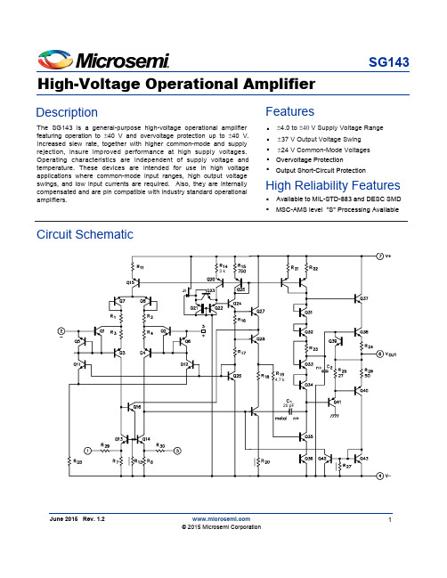
The SG143 is a general-purpose high-voltage operational amplifier featuring operation to ±40 V and overvoltage protection up to ±40 V. Increased slew rate, together with higher common-mode and supply rejection, insure improved performance at high supply voltages. Operating characteristics are independent of supply voltage and temperature. These devices are intended for use in high voltage applications where common-mode input ranges, high output voltage swings, and low input currents are required. Also, they are internally compensated and are pin compatible with industry standard operational amplifiers.High-Voltage Operational AmplifierSG143Description FeaturesJune 2015 Rev. 1.21 © 2015 Microsemi Corporation▪▪▪▪Overvoltage Protection±37 V Output Voltage Swing ±24 V Common-Mode Voltages ▪Output Short-Circuit ProtectionHigh Reliability Features▪Available to MIL-STD-883 and DESC SMD ▪MSC-AMS level "S" P rocessing A vailableCircuit Schematic3 k4.7 k20 pF±4.0 to ±40 V Supply Voltage RangeF igure5.I nput C urrentF igure 6. V oltageG ainF igure 1. P ower B andwidth F igure 2. P eak O utput V oltage S wing vs . P ower S upply V oltageF igure 4. O utput S hort -C ircuit C urrent vs . T emperatureF igure 3. O pen -L oop F requency R esponseCharacteristic Curves10 k+28 VV5 k Ω±28 VV 100 kΩ1.0 10 100 1.0 k 10 k 100 k 1.0 M 10 M 100 MNote 1. Contact factory for DESC product availablity.2. All packages are viewed from the top.F igure 8. U nityG ain B andwidthF igure 7. S upply C urrentAmbientTemperature Range Part No.PackageConnection Diagram-55°C to 125°C -55°C to 125°C SG143T -883B SG143T -DESC SG143T-55°C to 125°C8-PIN METAL CAN T - PACKAGEOUTPUTV+48517326INVERTING INPUT V -OFFSET ADJUST NON-INVERTING INPUTOFFSET ADJUSTN.C.8-PIN CERAMIC DIP Y- PACKAGESG143Y -DESC-55°C to 125°C87652134INVERTING INPUT OFFSET ADJUSTNON-INVERTING INPUTV-V+OFFSET ADJUSTOUTPUTN.C.F igure 11 - L ow - D rift S ample and H oldF igure 10 - D ifferential A mplifier with ±20 VF igure 9 - V oltage O ffset N ull C ircuitCharacteristic Curves (Continued)Typical ApplicationsConnection Diagrams and Ordering Information (See Notes Below )±28 V ±28 V10 k+28 V+28 V28 V10 k4.7 k10 k28 V100 kC ommon -M ode I nput V oltage R ange8 mV/s1.0 µF3.These hermetic packages use Sn63/Pb37 hot solder lead finish, contact factory for availability of RoHS versions.Microsemi Corporate Headquarters One Enterprise, Aliso Viejo,CA 92656 USAWithin the USA: +1 (800) 713-4113 Outside the USA: +1 (949) 380-6100 Sales: +1 (949) 380-6136Fax: +1 (949) 215-4996E-mail: ***************************Microsemi Corporation (MSCC) offers a comprehensive portfolio of semiconductor and system solutions for communications, defense & security, aerospace and industrial markets. Products include high-performance and radiation-hardened analog mixed-signal integrated circuits, FPGAs, SoCs and ASICs; power management products; timing and synchronization devices and precise time solutions, setting the world's standard for time; voice processing devices; RF solutions; discrete components; security technologies and scalable anti-tamper products; Ethernet solutions; Power-over-Ethernet ICs and midspans; as well as custom design capabilities and services. Microsemi is headquartered in Aliso Viejo, Calif., and has approximately 3,600 employees globally. Learn more at .© 2015 Microsemi Corporation. All rights reserved. Microsemi and the Microsemi logo are trademarks of Microsemi Corporation. All other trademarks and service marks are the property of their respective owners.Microsemi makes no warranty, representation, or guarantee regarding the information contained herein or the suitability of its products and services for any particular purpose, nor does Microsemi assume any liability whatsoever arising out of the application or use of any product or circuit. The products sold hereunder and any other products sold by Microsemi have been subject to limited testing and should not be used in conjunction with mission-critical equipment or applications. Any performance specifications are believed to be reliable but are not verified, and Buyer must conduct and complete all performance and other testing of the products, alone and together with, or installed in, any end-products. Buyer shall not rely on any data and performance specifications or parameters provided by Microsemi. It is the Buyer's responsibility to independently determine suitability of any products and to test and verify the same. The information provided by Microsemi hereunder is provided "as is, where is" and with all faults, and the entire risk associated with such information is entirely with the Buyer. Microsemi does not grant, explicitly or implicitly, to any party any patent rights, licenses, or any other IP rights, whether with regard to such information itself or anything described by such information. Information provided in this document is proprietary to Microsemi, and Microsemi reserves the right to make any changes to the information in this document or to any products and services at any time without notice.。
世伟洛克针阀资料(中文)
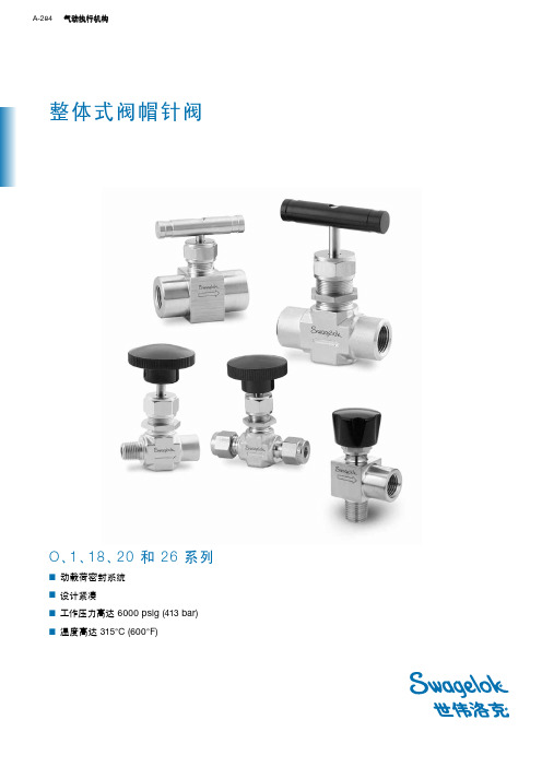
尺寸,in. (mm) 订购号 SS-ORS2 SS-1RS4 SS-1RS6 SS-1RS8 SS-18RS8 SS-18RS12 SS-ORS3MM SS-1RS6MM SS-1RS8MM SS-1RS10MM SS-1RS12MM SS-18RS12MM SS-18RS18MM SS-ORF2 SS-1RF2 SS-1RF4 SS-18RF6 SS-18RF8 SS-ORM2 SS-1RM2 SS-1RM4 SS-1RM6 SS-18RM8 SS-ORM2-S2 SS-1RM4-S4 SS-1RM4-S6 A 1.94
(9.5 mm)
B1 C
F E 孔口 0.375 in.
(9.5 mm)
流量系数 (Cv)
板装厚度 1/8 至 1/4
(3.2 至 6.4)带有调节杆的不锈钢阀门选择一订购号。
拧开的圈数
带有调节阀杆的 400 号合金、 铜和钢阀门
将订购号中的 SS 替换为材料标记。
调节阀杆 软座阀杆
材料 合金 400 铜 钢
A-284
气动执行机构
整 体 式 阀帽 针 阀
O、 1、 18 、20 和 26 系 列
■ 动载荷密封系统 ■ 设计紧凑 ■ 工作压力高达 6000 psig (413 bar) ■ 温度高达 315°C (600°F)
整体式阀帽针阀
A-285
特点
阀杆设计
■ V 型 —— 所有系列 ■ 软座 —— 所有系列 ■ 调节 —— O、 1 和 18 系列
O、1 和 18 系列
ASME 级别 材料级别 材料名称 温度,°C (°F) –53 (–65) 至 –28 (–20) –28 (–20) 至 37 (100) 93 (200) 121 (250) 148 (300) 176 (350) 204 (400) 232 (450) 260 (500) 315 (600) 5000 (344) 5000 (344) 4295 (295) 4085 (281) 3875 (266) 3715 (255) 3560 (245) 3435 (236) 3310 (228) 3130 (215) 2080 2.2 316 SS 铜 3000 (206) 3000 (206) 2350 (161) 2200 (151) 2050 (141) 1470 (101) 390 (26) — — — N/A N/A 钢 — 3000 (206) 2730 (188) 2695 (185) 2660 (183) 2615 (180) — — — — 工作压力,psig (bar) 3000 (206) 3000 (206) 2640 (181) 2555 (176) 2470 (170) 2430 (167) 2390 (164) 2380 (163) 2375 (163) — 1500 3.4 合金 400
BT134W-600四极体数据手册说明书

BT134W-6004Q Triac14 June 2016Product data sheet1. General descriptionPlanar passivated four quadrant triac in a SOT223 surface-mountable plastic package intended foruse in applications requiring high bidirectional transient and blocking voltage capability and highthermal cycling performance.2. Features and benefits•High blocking voltage capability•High noise immunity suitable for noisy applications•Planar passivated for voltage ruggedness and reliability•Surface-mountable package•Triggering in all four quadrants3. Applications•General purpose low power motor control•General purpose switching and phase control4. Quick reference data5. Pinning information6. Ordering information7. Marking8. Limiting values Table 5. Limiting values9. Thermal characteristics10. CharacteristicsT j (°C)-6014090-1040003aae9610.80.41.21.60V GT V GT (25°C)Fig. 13. Normalized gate trigger voltage as a function of junction temperature11. Package outline12. Package outline (minimized)13. Soldering14. Legal informationData sheet status[1]Please consult the most recently issued document before initiating orcompleting a design.[2]The term 'short data sheet' is explained in section "Definitions".[3]The product status of device(s) described in this document may havechanged since this document was published and may differ in case ofmultiple devices. The latest product status information is available onthe Internet at URL .DefinitionsDraft — The document is a draft version only. The content is still under internal review and subject to formal approval, which may result in modifications or additions. WeEn Semiconductors does not give any representations or warranties as to the accuracy or completeness of information included herein and shall have no liability for the consequences of use of such information.Short data sheet — A short data sheet is an extract from a full data sheet with the same product type number(s) and title. A short data sheet is intended for quick reference only and should not be relied upon to contain detailed and full information. For detailed and full information see the relevant full data sheet, which is available on request via the local WeEn Semiconductors sales office. In case of any inconsistency or conflict with the short data sheet, the full data sheet shall prevail.Product specification — The information and data provided in a Product data sheet shall define the specification of the product as agreed between WeEn Semiconductors and its customer, unless WeEn Semiconductors and customer have explicitly agreed otherwise in writing. In no event however, shall an agreement be valid in which the WeEn Semiconductors productis deemed to offer functions and qualities beyond those described in the Product data sheet.DisclaimersLimited warranty and liability — Information in this document is believedto be accurate and reliable. However, WeEn Semiconductors does notgive any representations or warranties, expressed or implied, as to the accuracy or completeness of such information and shall have no liability for the consequences of use of such information. WeEn Semiconductors takes no responsibility for the content in this document if provided by an information source outside of WeEn Semiconductors.In no event shall WeEn Semiconductors be liable for any indirect, incidental, punitive, special or consequential damages (including - without limitation -lost profits, lost savings, business interruption, costs related to the removal or replacement of any products or rework charges) whether or not such damages are based on tort (including negligence), warranty, breach of contract or any other legal theory.Notwithstanding any damages that customer might incur for any reason whatsoever, WeEn Semiconductors’ aggregate and cumulative liability towards customer for the products described herein shall be limited in accordance with the Terms and conditions of commercial sale of WeEn Semiconductors.Right to make changes — WeEn Semiconductors reserves the right to make changes to information published in this document, including without limitation specifications and product descriptions, at any time and without notice. This document supersedes and replaces all information supplied prior to the publication hereof.Suitability for use — WeEn Semiconductors products are not designed, authorized or warranted to be suitable for use in life support, life-criticalor safety-critical systems or equipment, nor in applications where failureor malfunction of an WeEn Semiconductors product can reasonablybe expected to result in personal injury, death or severe property or environmental damage. WeEn Semiconductors and its suppliers accept no liability for inclusion and/or use of WeEn Semiconductors products in such equipment or applications and therefore such inclusion and/or use is at the customer’s own risk.Quick reference data — The Quick reference data is an extract of the product data given in the Limiting values and Characteristics sections of this document, and as such is not complete, exhaustive or legally binding. Applications — Applications that are described herein for any of these products are for illustrative purposes only. WeEn Semiconductors makesno representation or warranty that such applications will be suitable for the specified use without further testing or modification.Customers are responsible for the design and operation of their applications and products using WeEn Semiconductors products, and WeEn Semiconductors accepts no liability for any assistance with applications or customer product design. It is customer’s sole responsibility to determine whether the WeEn Semiconductors product is suitable and fit for the customer’s applications and products planned, as well as for the planned application and use of customer’s third party customer(s). Customers should provide appropriate design and operating safeguards to minimize the risks associated with their applications and products.WeEn Semiconductors does not accept any liability related to any default, damage, costs or problem which is based on any weakness or defaultin the customer’s applications or products, or the application or use by customer’s third party customer(s). Customer is responsible for doing all necessary testing for the customer’s applications and products using WeEn Semiconductors products in order to avoid a default of the applicationsand the products or of the application or use by customer’s third party customer(s). WeEn does not accept any liability in this respect.Limiting values — Stress above one or more limiting values (as defined in the Absolute Maximum Ratings System of IEC 60134) will cause permanent damage to the device. Limiting values are stress ratings only and (proper) operation of the device at these or any other conditions above thosegiven in the Recommended operating conditions section (if present) or the Characteristics sections of this document is not warranted. Constant or repeated exposure to limiting values will permanently and irreversibly affect the quality and reliability of the device.No offer to sell or license — Nothing in this document may be interpreted or construed as an offer to sell products that is open for acceptance or the grant, conveyance or implication of any license under any copyrights, patents or other industrial or intellectual property rights.Export control — This document as well as the item(s) described herein may be subject to export control regulations. Export might require a prior authorization from competent authorities.Non-automotive qualified products — Unless this data sheet expressly states that this specific WeEn Semiconductors product is automotive qualified, the product is not suitable for automotive use. It is neither qualified nor tested in accordance with automotive testing or application requirements. WeEn Semiconductors accepts no liability for inclusion and/or use of non-automotive qualified products in automotive equipment or applications.In the event that customer uses the product for design-in and use in automotive applications to automotive specifications and standards, customer (a) shall use the product without WeEn Semiconductors’ warranty of the product for such automotive applications, use and specifications, and (b) whenever customer uses the product for automotive applications beyond WeEn Semiconductors’ specifications such use shall be solely at customer’s own risk, and (c) customer fully indemnifies WeEn Semiconductors forany liability, damages or failed product claims resulting from customer design and use of the product for automotive applications beyond WeEn Semiconductors’ standard warranty and WeEn Semiconductors’ product specifications.Translations — A non-English (translated) version of a document is for reference only. The English version shall prevail in case of any discrepancy between the translated and English versions.TrademarksNotice: All referenced brands, product names, service names and trademarks are the property of their respective owners.15. Contents1. General description (1)2. Features and benefits (1)3. Applications (1)4. Quick reference data (1)5. Pinning information (2)6. Ordering information (2)7. Marking (2)8. Limiting values (3)9. Thermal characteristics (6)10. Characteristics (8)11. Package outline (11)12. Package outline (minimized) (12)13. Soldering (12)14. Legal information (14)© WeEn Semiconductors Co., Ltd. 2016. All rights reservedFor more information, please visit: Forsalesofficeaddresses,pleasesendanemailto:**************************** Date of release: 14 June 2016。
VISHAY THIN FILM SOT-143 Resistor Network 数据手册

Molded, SOT -143 Resistor NetworkMPD/MPDAVishay Thin Film Fortechnicalquestions,contact:********************Document Number: 60016S U R F A C E M O U N T N E T W O R K SVISHAY Thin Film MPD Series Dividers provide ± 2 ppm/°C tracking and a ratio tolerance as tight as ± 0.05 %, small size, and exceptional stability for all surface mount applica-tions. The standard SOT -143 package format with unity and common standard resistance divider ratios provide easy selection for most applications requiring matched pair resis-tor elements. The ratios listed are available for off the shelf convenience, if you require a non-standard ratio, consult the applications engineering group as we may be able to meet your requirements with a custom design.FEATURES•Lead (Pb)-free available•Tight Ratio Tolerances to 0.05 %•± 2 ppm Tracking•Standard Values Stocked •Standard SOT-143 FootprintTYPICAL PERFORMANCENote: Tantalum Nitride film is available on special orders* Pb containing terminations are not RoHS compliant, exemptions may applyActual SizeABSTRACKINGTCR 252ABS RATIO TOL0.10.05STANDARD VALUESMODELR 2 (Ω)R 1 (Ω)R 3 (Ω)MPD100K 100K -50K 50K -25K 25K -20K 20K -10K 10K -5K 5K -2K 2K -1K 1K -MPDA10K10K 10KSTANDARD ELECTRICAL SPECIFICATIONSTEST SPECIFICATIONS CONDITIONS Material Passivated Nichrome TCR:Tracking ± 2 ppm/°C (typical)- 55 °C to + 125 °C Absolute ± 25 ppm/°C - 55 °C to + 125 °CTolerance:Ratio ± 0.5 % to ± 0.05 %+ 25 °C Absolute ± 1.0 % to ± 0.1 %+ 25 °C Power Rating:Resistor 100 mW Max. at + 70 °C Package 200 mW Max. at + 70 °C Stability:ΔR Absolute 0.10 %2000 hours at + 70 °C ΔR Ratio0.03 %2000 hours at + 70 °CVoltage Coefficient 0.1 ppm/V Working Voltage100 V Max.Operating Temperature Range - 55 °C to + 125 °C Storage Temperature Range - 55 °C to + 125 °CNoise< - 25 dB Thermal EMF0.2 µV/°C Shelf Life Stability (Ratio)50 ppm Max.1 year at + 25 °CMPD/MPDAMolded, SOT-143 Resistor NetworkVishay Thin FilmDocument Number: 60016Fortechnicalquestions,contact:********************SURFACE MOUNT NETWORKSDIMENSIONS AND IMPRINTING in millimetersDERATING CURVEMECHANICAL SPECIFICATIONSResistive Element Passivated NichromeSubstrate Material Silicon Body Molded epoxyT erminals Copper alloy #42 Sn62 platedLead Coplanarity 3 Mils Max.Lead (Pb)-free Option 100 % Sn MatteLead (Pb)-free FinishPlatedDIMENSION MIN.NOM.MAX.A 0.80- 1.22A10.05-0.15A20.750.90 1.07b 0.30-0.50b10.300.400.45b20.76-0.89b30.760.800.84c 0.08-0.20c10.080.100.16D 2.80 2.90 3.04E 2.10- 2.64E1 1.20 1.30 1.40e 1.92 BSC e10.20 BSC L 0.400.500.60L10.54 REF .N 4Ø0"-8"GLOBAL PART NUMBER INFORMATIONNew Global Part Numbering: MPD1002AWS (preferred part number format)GLOBAL MODEL(3 or 4 digits)RESIST ANCE (4 or 8 digits)TOLERANCE AND RATIO TOLERANCE PACKAGINGMPD(Two resistors Tin Lead)MPDT(Two resistors Lead(Pb)-free)(e3)The first 3 digits are significant figures and the last digit specifies the number of zeros to follow. When like values are required use total resistance.When dual values are required list both values.Example:1002 = 10K (5K/5K)1003 = 100K (50K/50K)Abs. T ol.A = ± 0.1 %B = ± 0.1 %C = ± 0.25 %D = ± 0.5 %F = ± 1 %Ratio ± 0.05 %± 0.1 %± 0.1 %± 0.1 %± 0.5 %BS = BULK 100 Min 1 Mult WS = WAFFLE 100 Min 1 Mult TAPE AND REELT1 = 1000 Min 1000 MultHistorical Part Number example: MPD1002BW (will continue to be accepted)MPD 1002BW SERIESRESIST ANCETOLERANCE AND RA TIO TOLERANCEPACKAGING PDT1M3BT1P D 1002MA W SMPD/MPDAVishay Thin FilmMolded, SOT-143 Resistor Network Fortechnicalquestions,contact:********************Document Number: 60016S U R F A C E M O U N T N E T W O R K SGLOBAL PART NUMBER INFORMATIONNew Global Part Numbering: MPDAT3002AWS (preferred part number format)GLOBAL MODEL (4 or 5 digits)RESISTANCETOLERANCE AND RATIO TOLERANCE PACKAGINGMPDA (Three equal series resistors Tin/lead)MPDAT (Three equal series resistors)(Lead (Pb)-free)(e3)irst 3 digits are significant figures and the last digit specifies the number of zeros to follow. When like values are required use total resistance.Example:3002 = Three 10 k Ω resistorsAbs. Tol.A = ± 0.1 %B = ± 0.1 %C = ± 0.25 %D = ± 0.5 %F = ± 1 %Ratio ± 0.05 %± 0.1 %± 0.1 %± 0.1 %± 0.5 %BS = BULK 100 Min 1 Mult WS = WAFFLE 100 Min 1 Mult T APE AND REELT1 = 1000 Min 1000 MultHistorical Part Number example: MPDA3002BT (will continue to be accepted)MPDA 3002BT SERIESRESISTANCETOLERANCE AND RATIO TOLERANCEPACKAGINGDAT32AWSMPD A 3002A W S MPLegal Disclaimer NoticeVishay Document Number: NoticeSpecifications of the products displayed herein are subject to change without notice. Vishay Intertechnology, Inc., or anyone on its behalf, assumes no responsibility or liability for any errors or inaccuracies.Information contained herein is intended to provide a product description only. No license, express or implied, by estoppel or otherwise, to any intellectual property rights is granted by this document. Except as provided in Vishay's terms and conditions of sale for such products, Vishay assumes no liability whatsoever, and disclaims any express or implied warranty, relating to sale and/or use of Vishay products including liability or warranties relating to fitness for a particular purpose, merchantability, or infringement of any patent, copyright, or other intellectual property right. The products shown herein are not designed for use in medical, life-saving, or life-sustaining applications. Customers using or selling these products for use in such applications do so at their own risk and agree to fully indemnify Vishay for any damages resulting from such improper use or sale.。
瑞丰GSRK14TS-ED(WE)产品说明书

Date :日期:1-8th Floor, Building #1,10th Industrial Zone, Tian Liao Community, Gong Ming Area, Guang Ming栋一至八楼Web/网址:Features特征 PLCC-2 Package. 垂直型表贴封装 Extremely wide viewing angle. 发光角度大Suitable for all SMT assembly and solder process. 适用于所有的SMT 组装和焊接工艺 Available on tape and reel. 适用于载带及卷轴 Moisture sensitivity level: 3. 防潮等级:3 Package:3000pcs/reel. 包装:3000颗/卷 RoHS compliant. RoHS 认证 Description 描述 The Yellow and Green source color devices are made with AlGaInP on Substrate Light Emitting Diode 黄绿光LED 由AlGaInP 四种元素芯片激发而成 Applications 应用 Optical indicator. 光学指示 Indoor display. 室内显示Landscape lighting,lamp belt. 景观照明,灯带等General suitable applications.其他适合的应用 RF-201709060119Package Dimension 封装尺寸 外形尺寸:2.0*1.4*1.3mmNOTES:备注1.All dimensions units are mm. (所有尺寸标注单位为毫米)2.All dimensions tolerances are 0.2mm unless otherwise noted. (除特别标注外,所有尺寸允许公差为±0.2毫米)Electrical / Optical Characteristics at Ts=25°C 电性与光学特性 Absolute Maximum Ratings at Ts=25°C 绝对最大值 Item 项目Symbol 符号test condition 测试条件Value unit 单位 Min. Max. Typ.Forward VoltageRank B1 VfIF=20mA1.8 1.92.1V Rank C2 1.9 2.0 V Rank C12.0 2.1 V Rank C2 2.1 2.2 V Rank D1 2.2 2.3 V Rank D2 2.3 2.4 V Dominant wavelengthRank B10 wld IF=20mA565.0567.5 570.5 nm Rank B20567.5 570.0 nm Rank C10 570.0 572.5 nm Rank C20 572.5 575.0 nm Luminous intensityRank 1ADIVIF=20mA28 40 49.3 mcd Rank 1AE 40 60 mcd Rank 1DM60 90 mcd Reverse Current IR VR=5V --- 10 --- uAViewing Angle 2Θ1/2 IF=20mA --- --- 120 Deg Thermal resistanceRth(j-s)IF=20mA------290 ℃/WParameter (参数) Symbol (符号)Rating (值)Units (单位)Power Dissipation (功耗) Pd 48 mW Forward Current (正向电流) IF 20 mA Peak Forward Current (峰值电流) IFP 100 mA Reverse Voltage (反向电压) VR 5 V Electrostatic Discharge(HBM)(静电) ESD 2000 V Operating Temperature (操作温度) Topr -40 ~ +85 ℃ Storage Temperature (储存温度) Tstg -40 ~ +100℃ junction temperature (结温) Tj90℃Note: 1. 1/10 Duty cycle, 0.1ms pulse width. 脉宽0.1ms,周期1/10.2. The above forward voltage measurement allowance tolerance is 0.1V. 以上所示电压测量误差0.1V.3. The above wavelength measurement allowance tolerance is ±1nm. 以上所示波长测量误差±1nm.4. the above luminous flux measurement allowance tolerance ±10%. 上述光通量的测试允许公差为±10%.5. Care is to be taken that power dissipation does not exceed the absolute maximum rating of the product. 使用功率不能超过规定的最大值.6. All measurements were made under the standardized environment of us. 所有测试都是基于我们现有的标准测试平台.7.When the LEDs are in operation the maximum current should be decided after measuring the package temperature,junction temperature should not exceed the maximum rate.LED使用的最大电流需要根据散热条件确定,结温不能超过最大值Handling Precautions 使用注意事项1>.LED operating environment and sulfur element composition cannot be over 100PPM in the LED mating usage material. This is provided for informational purposes only and is not a warranty or endorsement.LED工作环境及与LED适配的材料中,硫元素及化合物成份不可超过100PPM,单一的溴元素含量要求小于900PPM,单一氯元素含量要求小于900PPM,溴元素与氯元素总含量必须小于1500PPM(检测含量为与LED直接接触面上元素含量)。
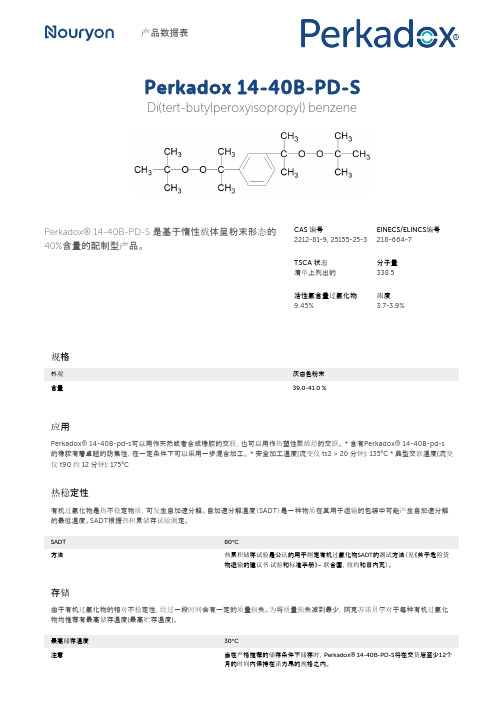
Perkadox 14-40B-PD-S 产品数据表说明书
产品数据表Perkadox 14-40B-PD-S Di(tert-butylperoxyisopropyl) benzenePerkadox® 14-40B-PD-S 是基于惰性载体呈粉末形态的40%含量的配制型产品。
CAS 编号2212-81-9, 25155-25-3EINECS/ELINCS编号218-664-7TSCA 状态清单上列出的分子量338.5活性氧含量过氧化物9.45%浓度3.7-3.9%规格外观灰白色粉末含量39.0-41.0 %应用Perkadox® 14-40B-pd-s可以用作天然或者合成橡胶的交联,也可以用作热塑性聚烯烃的交联。
* 含有Perkadox® 14-40B-pd-s的橡胶有着卓越的防焦性,在一定条件下可以采用一步混合加工。
* 安全加工温度(流变仪 ts2 > 20 分钟): 135°C * 典型交联温度(流变仪 t90 约 12 分钟): 175°C热稳定性有机过氧化物是热不稳定物质,可发生自加速分解。
自加速分解温度(SADT)是一种物质在其用于运输的包装中可能产生自加速分解的最低温度。
SADT根据热积累储存试验测定。
SADT80°C方法热累积储存试验是公认的用于测定有机过氧化物SADT的测试方法(见《关于危险货物运输的建议书·试验和标准手册》– 联合国,纽约和日内瓦)。
存储由于有机过氧化物的相对不稳定性,经过一段时间会有一定的质量损失。
为将质量损失减到最少,阿克苏诺贝尔对于每种有机过氧化物均推荐有最高储存温度(最高贮存温度)。
最高储存温度30°C注意当在严格推荐的储存条件下储存时,Perkadox® 14-40B-PD-S将在交货后至少12个月的时间内保持在诺力昂的规格之内。
包装和运输标准包装是25 kg 纸板箱。
包装和运输符合国际法规。
有关其他定量包装的可用性,请联系诺力昂销售代表。
SPR14资料

C1
元器件交易网
DIOTEC ELECTRONICS CORP.
18020 Hobart Blvd., Unit B Gardena, CA 90248 U.S.A Tel.: (310) 767-1052 Fax: (310) 767-7958
Data Sheet No. SESA-100-2B
PARAMETER (TEST CONDITIONS)
Series Number Maximum DC Blocking Voltage Maximum RMS Voltage Maximum Peak Recurrent Reverse Voltage Average Forward Rectified Current @ TA = 55 oC Peak Forward Surge Current ( 8.3mS single half sine wave superimposed on rated load) Maximum Forward Voltage at 1 Amp DC Maximum Average DC Reverse Current At Rated DC Blocking Voltage Typical Thermal Resistance, Junction to Ambient Typical Junction Capacitance (Note 1) Maximum Reverse Recovery Time (IF=0.5A, IR=1A, IRR=0.25A) Junction Operating and Storage Temperature Range
Sym
Polarity: Color band denotes cathode
Minimum In mm 0.160 0.103 1.00 0.028 4.1 2.6 25.4 0.71
- 1、下载文档前请自行甄别文档内容的完整性,平台不提供额外的编辑、内容补充、找答案等附加服务。
- 2、"仅部分预览"的文档,不可在线预览部分如存在完整性等问题,可反馈申请退款(可完整预览的文档不适用该条件!)。
- 3、如文档侵犯您的权益,请联系客服反馈,我们会尽快为您处理(人工客服工作时间:9:00-18:30)。
Welwyn Components
Specifications
Characteristic
Package Pow er Dissipat ion
Power Derating Curve
Value
0.25 Watt s @ 70° C 0.1 Watt s @ 70° C 100 Volt s
100
......................................................................... ......................................................................... ......................................................................... ......................................................................... .........................................................................
SOT143 Series Issue June 2006
元器件交易网
SOT143 4-PIN SMT Package
Environmental Data
Env i ronment al Tes t To MIL -PR F-83401 Thermal Shock Char act er i s t i c H L i mi t ±0.5% ±0.5% ±0.1% ±0.2%
4 3
1.0 ref.
0.43 min 0.51 max 0.076 min 0.178 max
2.36 ±0.25
1 2
1.30± 0.1
2.21ref. 0.79 min. 1.02 min 1.19 max.
1 2
0.84 ±0.1
0.635 ref.
0.56 ref.
General Note
© Welwyn Components Limited Bedlington, Northumberland NE22 7AA, UK
Telephone: +44 (0) 1670 822181 • Facsimile: +44 (0) 1670 829465 • Email: info@ • Website:
Temperature Coeff icient Tracking ±2ppm/° C Temperature Coeff icient Absolut e To ±25ppm/° C Operat ing Temperature Range -55° C t o +125° C M aximum Volt age Rat ing Element Pow er Dissipat ion
Ordering Procedure
Style SOT143 - 01 - A 002 - F B
Absolute TCR Code
00 = ±250ppm/°C; 01 = ±100ppm/°C 02 = ±50ppm/°C; 03 = ±25ppm/°C
A001 A002 A003 A004 A005
B001 B002 B003
Circuit Details for Schematic C
Schematic/Circuit Code
Circuit Details for Schematic D R3 (W) 10.0K 1.0K 1.0K 750.0 40.0K 330.0 2.0K 2.0K 200.0 10.0K
© Welwyn Components Limited Bedlington, Northumberland NE22 7AA, UK
A subsidiary of TT electronics plc SOT143 Series Issue June 2006
Telephone: +44 (0) 1670 822181 • Facsimile: +44 (0) 1670 829465 • Email: info@ • Website:
IRC Advanced Film Division
Max i mum ±0.1% ±0.1% ±0.1% ±0.1% ±0.f or mance ±0.02% ±0.03% ±0.02% ±0.05% ±0.03% ±0.03% ±0.05% ±0.02%
Termi nal St rengt h ±0.25% ±0.1% ±0.02% Resist ance to Solder Heat ±0.1% ±0.05% L ife ±0.5% M oi st ureResist ance ±0.4% L ow Temperat ure Operat i on ±0.1% Hi gh Temperat ure Exposure Short Ti me Overload Pow er Condi t i oni ng
Schematic/Circuit Code
R1 (W) N/A N/A N/A N/A N/A N/A N/A N/A N/A N/A
R2 (W) 10.0K 1.0K 9.0K 750.0 40.0K 33.0K 2.0K 10.0K 10.0K 2.1K
R1 (W) 121.0 2.0K 50.0K 5.4K 40.0K 10.0K 20.0K
R2 (W) 1.33K 1.0K 5.0K 5.4K 40.0K 10.0K 20.0K
R3 (W) 1.0K 2.0K 5.0K 27.5K 40.0K 20.0K 20.0K
C001 C002 C003 C004 C005 C006 C007 C008 C009 C010
D001 D002 D003 D004 D005 D006 D007
Schematic Code
A, B, C, D
Circuit Number
See Schematic/Circuit Detail Tables
Absolute Tolerance Code
K = ±10%; J = ±5%; G = ±2%; F = ±1% D = ±0.5%; C = ±0.25%; B = ±0.1%
1
2
Schematic D (bussed)
1
2
Schematic / Circuit Detail
Circuit Details for Schematic A
Schematic/Circuit Code
Circuit Details for Schematic B R3 (W) 50.0K 10.0K 9.0K 48.0K 40.0K
..................................................................................................................................................... ..................................................................................................................................................... ..................................................................................................................................................... ..................................................................................................................................................... ..................................................................................................................................................... ..................................................................................................................................................... ..................................................................................................................................................... .....................................................................................................................................................
Welwyn Components reserves the right to make changes in product specification without notice or liability. All information is subject to Welwyn’s own data and is considered accurate at time of going to print.
