HLMP-1719B0B01中文资料
HLMP-CM30-M00ZZ中文资料
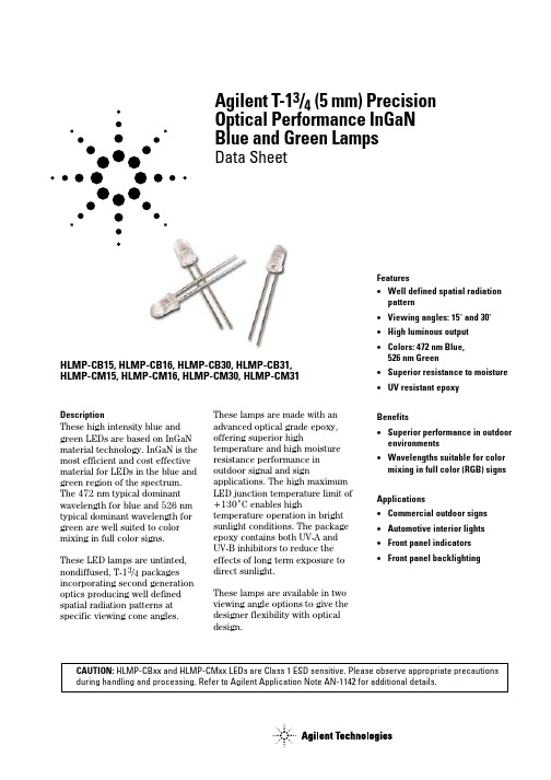
LED IndicatorsDevice Selection GuideColor andTypical Typ. Dominant Min. Luminous Typical ForwardViewing Wavelength Intensity, Iv Voltage Leads with Package Part Number Angleλd (nm)(mcd) at 20 mA(V) at 20 mA Stand-Offs Drawing HLMP-CB15-P00xx15°Blue 472880 3.8No A HLMP-CB15-R00xx15°Blue 4721500 3.5No A HLMP-CB15-QT0xx15°Blue 4721150 3.8No A HLMP-CB16-P00xx15°Blue 472880 3.8Yes B HLMP-CB16-QT0xx15°Blue 4721150 3.8Yes B HLMP-CB30-K00xx30°Blue 472310 3.8No A HLMP-CB30-KN0xx30°Blue 472310 3.8No A HLMP-CB30-M00xx30°Blue 472520 3.8No A HLMP-CB30-MQ0xx30°Blue 472520 3.8No A HLMP-CB30-NRGxx30°Blue 472680 3.8No A HLMP-CB31-M00xx30°Blue 472520 3.8Yes B HLMP-CB31-M0Gxx30°Blue 472520 3.8Yes B HLMP-CB31-NRGxx30°Blue 472680 3.8Yes B HLMP-CM15-S00xx15°Green 5261900 3.8No A HLMP-CM15-SV0xx15°Green 5261900 3.8No A HLMP-CM15-W00xx15°Green 5265500 3.5No A HLMP-CM15-VY0xx15°Green 5264200 3.8No A HLMP-CM16-S00xx15°Green 5261900 3.8Yes B HLMP-CM16-VY0xx15°Green 5264200 3.8Yes B HLMP-CM30-M00xx30°Green 526520 3.8No A HLMP-CM30-MQ0xx30°Green 526520 3.8No A HLMP-CM30-S00xx30°Green 5261900 3.5No A HLMP-CM30-TWAxx30°Green 5262500 3.8No A HLMP-CM31-M00xx30°Green 526520 3.8Yes B HLMP-CM31-TWAxx30°Green 5262500 3.8Yes BTolerance for intensity limit is ±15%.Part Numbering SystemHLMP - X X XX - X X X XXMechanical Options00: BulkDD: Ammo PackYY: Flexi bin, BulkZZ: Flexi bin, Ammo PackColor Bin Selection0: Full color rangeA: Color bin 1 & 2 onlyG: Color bin 2, 3 & 4 onlyMaximum Intensity Bin0: No maximum Iv bin limitOthers: Refer to Intensity Bin Limit TableMinimum Intensity BinRefer to Device Selection GuideViewing Angle and Standoff Options15: 15 degree without standoff16: 15 degree with standoff30: 30 degree without standoff31: 30 degree with standoffColorB: BlueM: GreenPackageC: T-1 3/4 (5 mm) round lampNotes:1. Dimensions in mm.2. Tolerance ±0.1 mm unless otherwise noted.5.80 ± 0.20 (0.039)HLMP-Cx15 and HLMP-Cx30Package Dimensions5.80 ± 0.20 (0.039)HLMP-Cx16 and HLMP-Cx31HLMP-Cx16HLMP-Cx31d = 12.60 ± 0.25 (0.496 ± 0.010) d = 12.22 ± 0.50 (0.481 ± 0.020)Absolute Maximum Ratings at T A = 25˚CParameter Blue and GreenDC Forward Current[1]30 mAPeak Pulsed Forward Current100 mAAverage Forward Current30 mAReverse Voltage (I R = 100 µA) 5 VPower Dissipation120 mWLED Junction Temperature130˚COperating Temperature Range–40˚C to +80˚CStorage Temperature Range–40˚C to +100˚CSoldering Temperature260˚C for 5 secondsNote:1.Derate linearly as shown in Figure 5 for temperatures above 50˚C.Electrical/Optical Characteristics at T A = 25˚CParameter Symbol Min.Typ.Max.Units Test Conditions Forward Voltage V F 3.5 4.0V I F = 20 mAReverse Voltage V R5I R = 100 µAPeak Wavelength Peak of Wavelength of Blue (λd = 472 nm)λpeak470nm Spectral Distribution Green (λd = 526 nm)524at I F = 20 mA Spectral Halfwidth Wavelength Width Blue (λd = 472 nm)∆λ1/235nm at Spectral Power Green (λd = 526 nm)47Point at I F = 20 mA Capacitance C43pF V F = 0, F = 1 MHz Luminous Efficacy Emitted Luminous Blue (λd = 472 nm)ηv75lm/W Power/Emitted Radiant Green (λd = 526 nm)520PowerThermal Resistance RΘJ-PIN240˚C/W LED Junction-to-Cathode LeadFigure 1. Relative intensity vs. wavelength.Figure 2. Forward current vs. forward voltage for devices with 3.5 V typical Vf.Figure 4. Relative luminous intensity vs.forward current.WAVELENGTH – nmR E L A T I V E I N T E N S I T Y1.0 0.9 0.8 0.7 0.6 0.5 0.4 0.3 0.2 0.100302515102.0 3.2520 2.82.4 3.6F O R W A R D C U R R E N TFORWARD VOLTAGE2.62.23.0 3.4 3.81.50.5I N T E N S I T Y N O R M A L I Z E D A T 20 m AI F – FORWARD CURRENT – mA 0515301.0102520Figure 5. Maximum forward current vs.ambient temperature.Figure 6. Spatial radiation pattern – 15˚ lamps.Figure 7. Spatial radiation pattern – 30˚ lamps.I F – F O R W A R D C U R R E N T – m AT A – AMBIENT TEMPERATURE – °C 40804035251510206010052030N O R M A L I Z E D I N T E N S I T Y1.00ANGULAR DISPLACEMENT – DEGREES0.80.60.2-300.41020-20-100300.90.70.50.30.1N O R M A L I Z E D I N T E N S I T Y1.0ANGULAR DISPLACEMENT – DEGREES 0.80.60.2-400.41020-20-10400.90.70.50.30.1-3030520550530D O M I N AN T W A V E L E N G T H – n mFORWARD CURRENT – mA540525535545Figure 8. Color vs. forward current.Figure 3. Forward current vs. forward voltage for devices with 3.8 V typical Vf.2.03.4V F – FORWARD VOLTAGE – V102530 I F – F O R W A R D C U R R E N T – m A4.251520 2.4 3.0 3.82.2 2.8 3.2 4.02.6 3.6Intensity Bin Limits Bin NameMin.Max.K 310400L 400520M 520680N 680880P 8801150Q 11501500R 15001900S 19002500T 25003200U 32004200V 42005500W 55007200X 72009300Y 930012000Z1200016000Tolerance for each intensity bin limit is ± 15%.Color Bin Limits (nm at 20 mA)Blue Color Range (nm)Bin ID Min.Max.1460.0464.02464.0468.03468.0472.04472.0476.05476.0480.0Tolerance for each bin limit is ± 0.5 nm.Green Color Range (nm)Bin ID Min.Max.1520.0524.02524.0528.03528.0532.04532.0536.05536.0540.0Tolerance for each bin limit is ± 0.5 nm.Note:1.All bin categories are established for classification of products. Products may not be available in all bin categories.Please contact your Agilent represen-tatives for further information./semiconductors For product information and a complete list of distributors, please go to our web site.For technical assistance call:Americas/Canada: +1 (800) 235-0312 or (916) 788-6763Europe: +49 (0) 6441 92460China: 10800 650 0017Hong Kong: (+65) 6271 2451India, Australia, New Zealand: (+65) 6271 2394 Japan: (+81 3) 3335-8152(Domestic/Interna-tional), or 0120-61-1280(Domestic Only) Korea: (+65) 6271 2194Malaysia, Singapore: (+65) 6271 2054 Taiwan: (+65) 6271 2654Data subject to change.Copyright © 2003 Agilent Technologies, Inc. Obsoletes 5988-8658ENAugust 1, 20035988-9962EN。
Met One Instruments BX-301 中文名字说明书

BX-301M ID R ANGE M EMBRANEI NSTRUCTIONSMet One Instruments, Inc.1600 NW Washington Blvd.Grants Pass, Oregon 97526Telephone 541-471-7111Facsimile 541-471-71161 About the BX-301 Mid-Range MembraneThe BX-301 is a special purpose mid-range membrane foil assembly which may be used to verify the linearity of the BAM-1020 mass calculation system. The mass calculation of the BAM-1020 is inherently linear in nature, and therefore it is unnecessary to audit a mid range point in the vast majority of applications. The BX-301 is provided only as a convenience to certain customers who may be required to perform the check by local regulations.The BAM-1020 unit performs a span membrane check automatically every hour using it’s built-in membrane with a mass of approximately 0.800 mg/cm2. The BX-301 allows the user to periodically perform an additional span check at about 0.500 mg/cm2.The BX-301 membrane is a fragile assembly, and must be handled very carefully. Any puncture or damage to the foil surface will render the part useless. Any dirt or contamination on the foil surface will be measured as mass, and will also invalidate the measurement. This assembly must be protected and stored in a safe location away from heat and direct sunlight.2 Mid Range Span Check ProcedureNote: The BAM-1020 unit must be powered on and warmed up for at least one hour before performing the test. The pump does not need to be running during warm-up.1. Remove the ten case cover screws and washers from the BAM-1020. You will needto access the inside of the unit later to complete the test.2. Verify the factory determined ABS value of the BAM-1020 unit. This can be found inthe SETUP > CALIBRATE menu or on the calibration certificate for the unit. This is the expected mass of the span membrane foil in the unit, and will be about 0.800mg/cm2.3. Enter the TEST > CALIBRATE menu on the user interface. This is the screen thatwill be used for the membrane tests. See Section 7.13 of the BAM-1020 manual.The CALIBRATE Test Screen4. Press the START soft key to start a membrane measurement with the existing foil.The test will take about eight minutes to complete. The unit will then display themeasured value of the span membrane foil as the CAL MASS M value. Comparethis value with the ABS (expected) value and record the results. These shouldtypically match within a few micrograms. Note: If these values disagree by 5% ormore, then there is something wrong with the unit such as a dirty membrane or an incorrect ABS value. Do not proceed with the test if the BAM-1020 is not reading its own membrane correctly.5. Remove the BAM case cover. Locate the membrane assembly on the inside of theunit, and the brass raceway in which the membrane assembly slides forwards and backwards. Remove the small dust cover (two small screws and washers). Set the parts aside.MembraneMotorDust CoverMembraneAssemblyMembraneControl ArmThe Membrane Assembly Inside the BAM-10206. Carefully remove the existing membrane from the unit: Pull back the control armagainst it’s spring pressure until you can slide the membrane from the back of the assembly. There should be an expected mass value printed on the back of the mid-range membrane. Record this value. Insert the mid-range membrane foil exactly as the other membrane was installed. Note: Make sure the pin of the membrane is in the slot of the control arm, or the test will not work. Swapping membranes is a very simple matter once you know what you are doing.7. Press the START soft-key to start the test with the mid-range membrane in place.When the unit has calculated and displayed the new CAL MASS M value, record it and start the test over. Perform the test two more times and take an average of the three measured values. This average must be within 5% of the expected valueprinted on the membrane, and will typically be within a few micrograms. Record the results.8. Remove the mid-range membrane and replace the original part. Reinstall the smalldust cover and the main case cover of the BAM-1020.BAM-1020 Membrane Foil Mid-Range Linearity CheckTest Results Record:Test Performed By:Test Date:BAM-1020 Serial Number:Expected ABS Value:mg/cm2Measured Mass of Existing Foil:mg/cm2Difference:mg/cm2Difference %:%Expected Mass of Mid-Range Foil:mg/cm2Measured Mid-Range Mass, Test 1:mg/cm2Measured Mid-Range Mass, Test 2:mg/cm2Measured Mid-Range Mass, Test 3:mg/cm2Average Mid-Range Mass:mg/cm2Difference from Expected Value:mg/cm2Difference %:%。
斗轮机扁平控制电缆参数赫杰姆-概述说明以及解释

斗轮机扁平控制电缆参数赫杰姆-概述说明以及解释1.引言1.1 概述概述部分的内容可以从以下几个方面进行展开。
斗轮机扁平控制电缆参数赫杰姆是现代工程领域中的一项关键技术,主要应用于斗轮机的控制系统中。
斗轮机是一种用于装载和卸载散装物料的重型机械设备,常见于港口、矿山等场所。
它的工作原理是通过大型旋转的斗轮来托起和运输物料。
在斗轮机的控制系统中,扁平控制是一种重要的控制策略,它的核心思想是将控制系统分解成多个层次,每个层次都有特定的控制目标和功能。
相比传统的集中式控制系统,扁平控制具有更好的灵活性和可扩展性,能够更好地应对不同的工况和需求变化。
电缆参数赫杰姆是扁平控制中的一个重要组成部分,它主要用于传输控制信号和数据。
电缆参数赫杰姆是指电缆的物理特性和电气特性,包括电缆的截面积、绝缘材料、传输速度等。
合理选择和设计电缆参数赫杰姆,能够保证控制信号的稳定传输和系统的可靠运行。
本文将从斗轮机扁平控制和电缆参数赫杰姆两个方面进行详细介绍和分析。
在斗轮机扁平控制部分,将介绍扁平控制的基本理论和关键技术,以及其在斗轮机控制系统中的应用。
在电缆参数赫杰姆部分,将重点讨论影响电缆参数赫杰姆的因素和如何选择合适的电缆参数赫杰姆。
通过本文的研究,可以更好地理解斗轮机扁平控制和电缆参数赫杰姆的关键技术和应用,为斗轮机控制系统的设计和优化提供科学的理论依据和实践经验。
同时,对于其他重型机械设备的控制系统设计和优化也具有一定的借鉴意义。
综上所述,本文将从斗轮机扁平控制和电缆参数赫杰姆两个方面进行深入研究和分析,旨在为相关领域的工程技术人员和研究人员提供有益的参考和指导。
文章结构在本文中,我们将以斗轮机扁平控制电缆参数赫杰姆为主题进行讨论。
文章分为引言、正文和结论三部分,各部分的内容安排如下:1. 引言1.1 概述:我们将首先介绍斗轮机扁平控制的背景和意义,以及电缆参数赫杰姆在该领域的应用。
1.2 文章结构:本部分将详细说明文章的结构和各个部分的内容安排,以帮助读者更好地理解文章的整体架构。
P171中文资料

P171-Type PIN/Preamp Advance Data Sheet November 2000The P171-Type PIN/Preamp features a rear-illuminated planar diode structure with low capacitance.Featuress Low-profile, 4-lead mini-DIL package:— Suitable for SONET applicationss Optional differential output in a 6-lead mini-DIL packages Transimpedance amplifier with automatic gain control (AGC)s Metal package:— Offers superior shielding for high noise immunitys High performance:— High speed (<0.5 ns typical rise and fall time)— High responsivity (0.85 A/W typical)— Low dark currents Planar structure for high reliabilitys Wavelength: 1.1 µm—1.6 µms50 µm core multimode fibers Wide operating temperature range:— –40 °C to +85 °Cs Wide bandwidths Qualification program: Telcordia Technologies* TA-NWT-983s Typical sensitivity:— –38 dBm at 155 Mbits/s— –33 dBm at 622 Mbits/sApplicationss Long-reach SONET OC-3/OC-12 and SDH STM-1/STM-4 telecommunications applicationss Secure digital data systemss Line terminal equipmentBenefitss Compact sizes Easily board mounted* Telcordia Technologies is a registered trademark of Telcordia Technologies, Inc.元器件交易网Advance Data SheetP171-Type PIN/PreampNovember 20002Agere Systems Inc.元器件交易网元器件交易网Advance Data SheetNovember 2000P171-Type PIN/Preamp元器件交易网Advance Data SheetP171-Type PIN/Preamp November 2000元器件交易网Advance Data SheetNovember 2000P171-Type PIN/Preamp元器件交易网Advance Data SheetP171-Type PIN/Preamp November 2000元器件交易网Advance Data SheetNovember 2000P171-Type PIN/PreampAdvance Data SheetP171-Type PIN/PreampNovember 2000For additional information, contact your Agere Systems Account Manager or the following:INTERNET: E-MAIL: docmaster@N. AMERICA:Agere Systems Inc., 555 Union Boulevard, Room 30L-15P-BA, Allentown, P A 18109-32861-800-372-2447 , FAX 610-712-4106 (In CANADA: 1-800-553-2448 , FAX 610-712-4106)ASIA PACIFIC:Agere Systems Singapore Pte. Ltd., 77 Science Park Drive, #03-18 Cintech III, Singapore 118256Tel. (65) 778 8833 , FAX (65) 777 7495CHINA:Agere Systems (Shanghai) Co., Ltd., 33/F Jin Mao Tower, 88 Century Boulevard Pudong, Shanghai 200121 PRCTel. (86) 21 50471212 , FAX (86) 21 50472266JAP AN:Agere Systems Japan Ltd., 7-18, Higashi-Gotanda 2-chome, Shinagawa-ku, Tokyo 141, JapanTel. (81) 3 5421 1600 , FAX (81) 3 5421 1700EUROPE:Data Requests: DATALINE: Tel. (44) 7000 582 368 , FAX (44) 1189 328 148Technical Inquiries: OPTOELECTRONICS MARKETING: (44) 1344 865 900 (Ascot UK)Agere Systems Inc. reserves the right to make changes to the product(s) or information contained herein without notice. No liability is assumed as a result of their use or application.Copyright © 2001 Agere Systems Inc.All Rights ReservedNovember 2000DS00-126OPTO-1 (Replaces DS00-126OPTO)Ordering Information*LR = meets SONET long-reach specifications.†>LR = exceeds SONET long-reach specifications.Device Code DescriptionComcode P171B014BAA 155 MHz Preamp, LR * , 4 Pins, 50 µ m Fiber, SC 108156704P171B014BAF 155 MHz Preamp, LR, 4 Pins, 50 µ m Fiber, FC/PC 108156712P171A016BAA 155 MHz Preamp, LR, 6 Pins, 50 µ m Fiber, SC 108316373P171A016BAF 155 MHz Preamp, LR, 6 Pins, 50 µ m Fiber, FC/PC 108316381P171B046BAA 622 MHz Preamp, >LR † , 6 Pins, 50 µ m Fiber, SC 108695461P171B046BAF622 MHz Preamp, >LR, 6 Pins, 50 µm Fiber, FC/PC108695479元器件交易网。
1719 Ex I O EtherNet IP Adapter 产品说明书
Release Notes1719 Ex I/O EtherNet/IP AdapterFirmware Revision 2.013Catalog Number 1719-AENTRTopic PageAbout This Publication1Before You Begin1Firmware Revision History2Enhancements2Known Anomalies3Additional Resources3About This PublicationThese release notes supplement the existing documentation that is supplied with your product. Read this document before using your 1719 Ex I/O EtherNet/IP Adapter with firmware revision 2.013.Before You BeginCompatibilityThe 1719-AENTR Add-on Profile is compatible with the following:•Studio 5000 Logix Designer® application, version 24 or later•RSLinx® software, version 3.74 or later2 1719 Ex I/O EtherNet/IP AdapterRockwell Automation Publication 1719-RN002C-EN-E - September 2017Y ou can download Add-on Profiles from the following web page:https:///rockwellautomation/support/downloads.pageFirmware Revision HistoryThe following tables provide a list of enhancements and known anomalies for the 1719 Ex I/O EtherNet/IP Adapter firmware revision.EnhancementsFirmware Revision History for 1719 Ex I/O EtherNet/IP AdapterRevision Description 2.011First revision released.2.012Second revision released.2.013Third revision released.Enhancements for Firmware Revision 2.013EnhancementDescriptionImproved LCD screen contrastThe adapter LCD screen display has changed from grayscale to monochrome to further improve the display contrast.Enhancements for Firmware Revision 2.012EnhancementDescriptionUpdated HART object definitionsThe 1719 HART object definitions have been updated to improve collection and notification of new or changed HART device information.Improved LCD screen display at low temperatureThe adapter LCD screen display at low temperature has been improved.1719 Ex I/O EtherNet/IP Adapter 3Rockwell Automation Publication 1719-RN002C-EN-E - September 2017Known AnomaliesAdditional ResourcesThese documents contain additional information concerning related products from Rockwell Automation.Y ou can view or download publications at/literature/. T o order paper copies of technical documentation, contact your local Allen-Bradley distributor or Rockwell Automation sales representative.Known Anomalies for Firmware Revision 2.011EnhancementDescriptionIP address 0.0.0.0 displays if there is no network connectionThe adapter LCD displays the IP address 0.0.0.0 on the start screen if there is no network connection identified.You must connect an Ethernet cable to one of the adapter Ethernet ports to display the current IP address.LCD screen may display low contrast at low temperatureThe adapter LCD screen may display with low contrast at -10 °C and the readability may be affected at -20 °C.ResourceDescription1719 Ex I/O Installation Instructions, publication 1719-IN001Describes how to install and wire the 1719 Ex I/O modules.1719 Ex I/O User Manual, publication 1719-UM001 Provides information on using the 1719 Ex I/O modules, backplanes, and accessories.1719 Ex I/O Technical Data, publication 1719-TD001 Provides specifications, wiring diagrams, and module block diagrams for 1719 Ex I/O.Industrial Automation Wiring and Grounding Guidelines, publication 1770-4.1Provides general guidelines for installing a Rockwell Automation industrial system.Product Certifications website,/global/certification Provides declarations of conformity, certificates, and other certification details.Publication 1719-RN002C-EN-E - September 2017Supersedes Publication 1719-RN002B-EN-E - July 2017Copyright © 2017 Rockwell Automation, Inc. All rights reserved.Allen-Bradley, Rockwell Software, Rockwell Automation, RSLinx, and Studio 5000 Logix Designer are trademarks of Rockwell Automation, Inc.T rademarks not belonging to Rockwell Automation are property of their respective companies.Rockwell Automation SupportRockwell Automation provides technical information on the Web to assist you in using its products.At /support you can find technical and application notes, sample code, and links to software service packs. You can also visit our Support Center at https:/// for software updates, support chats and forums, technical information, FAQs, and to sign up for product notification updates.In addition, we offer multiple support programs for installation, configuration, and troubleshooting. For more information, contact your local distributor or Rockwell Automation representative, or visit /services/online-phone .Installation AssistanceIf you experience a problem within the first 24 hours of installation, please review the information that's contained in this manual. You can also contact a special Customer Support number for initial help in getting your product up and running.New Product Satisfaction ReturnRockwell Automation tests all of its products to help ensure that they are fully operational when shipped from the manufacturing facility. However, if your product is not functioning and needs to be returned, follow these procedures.Documentation FeedbackYour comments will help us serve your documentation needs better. If you have any suggestions on how to improve this document, complete this form, publication RA-DU002, available at /literature/.United States or Canada1.440.646.3434Outside United States or Canada Use the Worldwide Locator at/rockwellautomation/support/overview.page , orcontact your local Rockwell Automation representative.United States Contact your distributor. You must provide a Customer Support case number (call the phone number above to obtain one) to your distributor to complete the return process.Outside United StatesPlease contact your local Rockwell Automation representative for the return procedure.Rockwell Otomasyon Ticaret A.Ş., Kar Plaza İş Merkezi E Blok Kat:6 34752 İçerenköy, İstanbul, T el: +90 (216) 5698400Rockwell Automation maintains current product environmental information on its website at/rockwellautomation/about-us/sustainability-ethics/product-environmental-compliance.page .。
HLMP-BL11-N0T00中文资料

Agilent HLMP-ABxx, HLMP-BBxx, HLMP-ADxx, HLMP-BDxx, HLMP-AGxx, HLMP-BGxx, HLMP-ALxx, HLMP-BLxx,HLMP-AMxx, HLMP-BMxx T-13/4 (5 mm)Oval Precision Optical Performance AlInGaP and InGaN Lamps Data SheetFeatures•Well defined spatial radiation pattern•Viewing angles:Major axis 70°Minor axis 35°•High luminous output•Red and Amber Intensity are available for:AlInGaP (Bright)AlInGaP II (Brightest)•Colors:472 nm blue 526 nm green 626 nm red 630 nm red 590 nm amber 592 nm amber•Superior resistance to moisture •UV resistant epoxyBenefits•Viewing angle designed for wide field of view application•Red, green, and blue radiation patterns matched for full color sign•Superior performance in outdoor environments Applications•Full color/video signsDescriptionThese Precision O ptical Performance Oval LEDs are specifically designed for full color/video and passenger information signs. The oval shaped radiation pattern(35°x 70°) and high luminous intensity ensure that these devices are excellent for wide field of view outdoor application where a wide viewing angle and readability in sunlight areessential. These lamps have very smooth, matched radiation patterns ensuring consistent color mixing in full colorapplications, message uniformity across the viewing angle of the sign.High efficiency LED material is used in these lamps: Aluminum Indium Gallium Phosphide (AlInGaP) for amber and red,and Indium Gallium Nitride(InGaN) for blue and green. Each lamp is made with an advance optical grade epoxy offering superior high temperature and high moisture resistance in outdoor applications. The package epoxy contains both UV-A and UV-B inhibitors to reduce the effects of long term exposure to direct sunlight.Designers can select parallel or perpendicular orientation. Both lamps are available in tinted version.CAUTION: The blue and green LEDs are Class 1 ESD sensitive. Please observe appropriate precautions during handling and processing. Refer to Agilent Application Note AN-1142 for additio nal details.Table 1. Device Selection Guide for AlInGaP IIColor and Luminous Luminous ForwardDominant Intensity,Intensity,Voltage,LeadsWavelength I v (mcd) at I v (mcd) at V f (V)with Leadframe Package Part Numberλd (nm) Typ.20 mA Min.20 mA Max.Max.Stand-offs Orientation Drawing HLMP-AD06-P00xx Red 630880 2.4No Parallel A HLMP-AD06-P0Txx Red 630880 2.6No Parallel A HLMP-AD16-P00xx Red 630880 2.4Yes Parallel B HLMP-AD16-P0Txx Red 630880 2.6Yes Parallel B HLMP-AD16-RS0xx Red 63015002500 2.6Yes Parallel B HLMP-AD16-RSTxx Red 63015002500 2.6Yes Parallel B HLMP-AD16-RU0xx Red 63015004200 2.4Yes Parallel B HLMP-AD16-RUTxx Red 63015004200 2.6Yes Parallel B HLMP-AD16-ST0xx Red 63019003200 2.4Yes Parallel B HLMP-AD16-STTxx Red 63019003200 2.6Yes Parallel B HLMP-AL06-L00xx Amber 592400 2.4No Parallel A HLMP-AL06-L0Rxx Amber 592400 2.6No Parallel A HLMP-AL06-N00xx Amber 592680 2.4No Parallel A HLMP-AL06-N0Rxx Amber 592680 2.6No Parallel A HLMP-AL16-N00xx Amber 592680 2.4Yes Parallel B HLMP-AL16-N0Rxx Amber 592680 2.6Yes Parallel B HLMP-AL16-PSRxx Amber 5928802500 2.6Yes Parallel B HLMP-AL16-QR0xx Amber 59211501900 2.4Yes Parallel B HLMP-AL16-QRRxx Amber 59211501900 2.6Yes Parallel B HLMP-BD06-P00xx Red 630880 2.4No Perpendicular C HLMP-BD06-P0Txx Red 630880 2.6No Perpendicular C HLMP-BD06-RS0xx Red 63015002500 2.4No Perpendicular C HLMP-BD06-RSTxx Red 63015002500 2.6No Perpendicular C HLMP-BD16-P00xx Red 630880 2.4Yes Perpendicular D HLMP-BD16-P0Txx Red 630880 2.6Yes Perpendicular D HLMP-BD16-RU0xx Red 63015004200 2.4Yes Perpendicular D HLMP-BD16-RUTxx Red 63015004200 2.6Yes Perpendicular D HLMP-BD16-ST0xx Red 63019003200 2.4Yes Perpendicular D HLMP-BD16-STTxx Red 63019003200 2.6Yes Perpendicular D HLMP-BL06-N00xx Amber 592680 2.4No Perpendicular C HLMP-BL06-N0Rxx Amber 592680 2.6No Perpendicular C HLMP-BL06-QRKxx Amber 59211501900 2.4No Perpendicular C HLMP-BL06-QRSxx Amber 59211501900 2.6No Perpendicular C HLMP-BL16-N00xx Amber 592680 2.4Yes Perpendicular D HLMP-BL16-N0Rxx Amber 592680 2.6Yes Perpendicular D HLMP-BL16-PS0xx Amber 5928802500 2.4Yes Perpendicular D HLMP-BL16-PSRxx Amber 5928802500 2.6Yes Perpendicular DTable 2. LED IndicatorsDevice Selection Guide for AlInGaPColor and Luminous LuminousDominant Intensity,Intensity,LeadsWavelength I v (mcd) at I v (mcd) at with Leadframe Package Part Numberλd (nm) Typ.20 mA Min.20 mA Max.Stand-offs Orientation Drawing HLMP-AG01-K00xx Red 626310No Parallel A HLMP-AG11-KN0xx Red 626310880Yes Parallel B HLMP-AL01-K00xx Amber 590310No Parallel A HLMP-AL01-LP0xx Amber 5904001150No Parallel A HLMP-AL01-NR0xx Amber 5906801900No Parallel A HLMP-AL11-KN0xx Amber 590310880Yes Parallel B HLMP-AL11-NR0xx Amber 5906801900Yes Parallel B HLMP-BG01-LM0xx Red 626400520No Perpendicular C HLMP-BG01-MN0xx Red 626520880No Perpendicular C HLMP-BG11-KN0xx Red 626310880Yes Perpendicular D HLMP-BL01-NR0xx Amber 5906801900No Perpendicular C HLMP-BL11-KN0xx Amber 590310880Yes Perpendicular D HLMP-BL11-NR0xx Amber 5906801900Yes Perpendicular DTable 3. Device Selection Guide for InGaNColor and Dominant Luminous Intensity,Leads with Leadframe Package Part Number Wavelength λd (nm) Typ. Iv (mcd) at 20 mA Min.Stand-offs Orientation Drawing HLMP-AB01-J00xx Blue 472240No Parallel A HLMP-BB11-J00xx Blue 472240Yes Perpendicular D HLMP-BB11-K00xx Blue 472310Yes Perpendicular D HLMP-BM11-L00xx Green 526400Yes Perpendicular D HLMP-BM11-Q00xx Green 5261150Yes Perpendicular D HLMP-AB11-J00xx Blue 472240Yes Parallel B HLMP-AM01-Q00xx Green 5261150No Parallel A HLMP-BB01-J0Bxx Blue 472240No Perpendicular C HLMP-BB11-KN0xx Blue 472310Yes Perpendicular D HLMP-BM01-L00xx Green 526400No Perpendicular C Tolerance for intensity range limit is ±15%.Part Numbering SystemHLMP-X X X X - X X X XXMechanical Options00: Bulk PackagingDD: Ammo PackYY: Flexi-Bin; Bulk PackagingZZ: Flexi-Bin; Ammo PackColor Bin0: No Color Bin LimitationR: Color Bins 1, 2, 4, and 6 with V F max of 2.6 VT: Red Color with V F max of 2.6 VB: Color bin 2 and 3 onlyK: Color bins 2 and 4 onlyS: Color bins 2 and 4 with VF max of 2.6 VMaximum Intensity Bin0: No Iv Bin LimitationMinimum Intensity BinTint Option1 or 6: Matching Color TintsStandoff Option0: Without1: WithColorB: 472 nm BlueD: 630 nm RedG: 626 nm RedL: 590 or 592 nm AmberM: 526 nm GreenPackageA: 5 mm 35° x 70° Oval, ParallelB: 5 mm 35° x 70° O val, PerpendicularPackage Dimensions5.00 ±(0.197 ±8.71 ± 0.200.50 ± 0.10SQ. TYP.5.00 ±(0.197 ±5.00 ±(0.197 ±5.00 ±(0.197 ±ABCDNOTES:1. ALL DIMENSIONS ARE IN MILLIMETERS (INCHES).2. LEADS ARE MILD STEEL, SOLDER DIPPED.3. TAPERS SHOWN AT TOP OF LEADS (BOTTOM OF LAMP PACKAGE) INDICATE AN EPOXY MENISCUS THAT MAY EXTEND ABOUT 1 mm (0.040 IN.) DOWN THE LEADS.4. RECOMMENDED PC BOARD HOLE DIAMETERS:– LAMP PACKAGES A AND C WITHOUT STAND-OFFS: FLUSH MOUNTING AT BASE OF LAMP PACKAGE = 1.143/1.067 mm (0.044/0.042 IN.).– LAMP PACKAGES B AND D WITH STAND-OFFS: MOUNTING AT LEAD STAND-OFFS.Absolute Maximum Ratings at T A = 25˚CParameter Blue and Green Red and Amber DC Forward Current[1]30 mA50 mAPeak Pulsed Forward Current[2]100 mA100 mAAverage Forward Current30 mA30 mAReverse Voltage (I R = 100 µA) 5 VReverse Voltage (I R = 10 µA) 5 VPower Dissipation120 mW120 mWLED Junction Temperature130°C130°COperating Temperature Range–40°C to +80°C–40°C to +100°C Storage Temperature Range–40°C to +100°C–40°C to +120°C Wave Soldering Temperature[3]250°C for 3 seconds250°C for 3 seconds Notes:1.Derate linearly from Figure 7.2.Duty Factor 30% KHz.3.1.59 mm (0.060 in.) below body.Electrical/Optical Characteristics at T A = 25°CParameter Symbol Min.Typ.Max.Units Test Conditions Typical Viewing AngleMajor2θ1/270degMinor35Forward Voltage V F V I F = 20 mARed (λd = 626 nm) 2.0 2.4Red (λd = 630 nm)Option xx0xx 2.2 2.4Option xxTxx 2.3 2.6Amber (λd = 590 nm) 2.0 2.4Amber (λd = 592 nm)Option xx0xx 2.2 2.4Option xxRxx, xxSxx 2.3 2.6Blue (λd = 472 nm) 3.5 4.0Green (λd = 526 nm) 3.5 4.0Reverse VoltageAmber, Red V R520V I R = 100 µABlue, Green5–I R = 10 µAPeak Wavelength Peak of Wavelength of Amber (λd = 592 nm)λpeak594nm Spectral Distribution Red (λd = 630 nm)639at I F = 20 mABlue (λd = 472 nm)470Green (λd = 526 nm)524Spectral Halfwidth Wavelength Width Amber (λd = 592 nm)∆λ1/217nm at Spectral Distribution Red (λd = 630 nm)171/2 Power Point at Blue (λd = 472 nm)35I F = 20 mAGreen (λd = 526 nm)47Capacitance V F = 0, F = 1 MHz Amber, Red C40pFBlue, Green43Luminous Efficacy Emitted Luminous Amber (λd = 592 nm)ηv500lm/W Power/Emitted Radiant Red (λd = 630 nm)155Power at I F = 20 mA Blue (λd = 472 nm)75Green (λd = 526 nm)520Thermal Resistance RΘJ-PIN240°C/W LED Junction-to-Cathode LeadNotes:1.2θ1/2 is the off-axis angle where the luminous intensity is 1/2 the on-axis intensity.2.The radiant intensity, I e in watts per steradian, may be found from the equation I e = I v/ηv where I v is the luminous intensity in candelas and ηv isthe luminous efficacy in lumens/watt.3.The luminous intensity is measured on the mechanical axis of the lamp package.4.The optical axis is closely aligned with the package mechanical axis.5.The dominant wavelength, λd, is derived from theCIE Chromaticity Diagram and represents the color of the lamp.6.For Options -xxRxx, -xxSxx and -xxTxx, max. forward voltage (Vf) is 2.6 V. Refer to Vf bin table.Figure 1. Relative intensity vs. wavelength.Figure 2. Blue, green forward current vs.forward voltage.WAVELENGTH – nmR E L A T I V E I N T E N S I T Y1.00.500.40.30.20.10.60.70.80.9030251510I F – F O R W A R D C U R R E N T – m AV F – FORWARD VOLTAGE – V2.42.83.2 3.6520 2.6 3.0 3.4Figure 3a. Amber, red forward current vs.forward voltage.Figure 4. Blue, green relative luminous intensity vs. forward current.1.50.5I N T E N S I T Y N O R M A L I Z E D A T 20 m AI F – FORWARD CURRENT – mA01020301.051525C U R R E N T – m AV F – FORWARD VOLTAGE – V Figure 3b. Forward current vs. forward voltage for option -xxTxx red, and option -xxRxx and -xxSxx amber.D C F O R W A R D C U R RE N T – m AFORWARD VOLTAGE – VFigure 6. Blue, green maximum forward current vs. ambient temperature.Figure 7. Amber, red maximum forward current vs. ambient temperature.I F – F O R W A R D C U R R E N T – m A0T A – AMBIENT TEMPERATURE – °C40804020102060301005152535I F – F O R W A R D CU R R E N T – m AT A – AMBIENT TEMPERATURE – °CFigure 5. Amber, red relative luminous intensity vs. forward current.R E L A T I V E I N T E N S I T Y (N OR M A L I Z E D A T 20 m A )FORWARD CURRENT – mAFigure 8. Spatial radiation pattern – 35 x 70 degree lamps.R E L A T I V E I N T E N S I T Y – %1000VERTICAL ANGULAR DISPLACEMENT – DEGREES8060507020501030404020-10-30-50903010-20-40R E L A T I V E I N T E N S I T Y – %1000HORIZONTAL ANGULAR DISPLACEMENT – DEGREES8060507020501030404020-10-30-50903010-20-40Intensity Bin Limits (mcd at 20 mA)Bin Name Min.Max.G 140180H 180240J 240310K 310400L 400520M 520680N 680880P 8801150Q 11501500R 15001900S 19002500T 25003200U19002500Tolerance for each bin limit is ±15%.Amber Color Bin Limits (nm at 20 mA)Bin Name Min.Max.1584.5587.02587.0589.54589.5592.06592.0594.5Tolerance for each bin limit is ± 0.5 nm.Notes:1.All bin categories are established for classifi-cation of products. Products may not beavailable in all bin categories. Please contact your Agilent representative for further information.2. Vf bin table only available for those numbers with options -xxRxx, -xxSxx, -xxTxx.Blue Color Bin Limits (nm at 20 mA)Bin Name Min.Max.1460.0464.02464.0468.03468.0472.04472.0476.05476.0480.0Tolerance for each bin limit is ± 0.5 nm.Green Color Bin Limits (nm at 20 mA)Bin Name Min.Max.1520.0524.02524.0528.03528.0532.04532.0536.05536.0540.0Tolerance for each bin limit is ±0.5 nm.Vf Bin Table [2]Bin Id Min.Max.VA 2.0 2.2VB 2.2 2.4VC2.4 2.6/semiconductors For product information and a complete list of distributors, please go to our web site.For technical assistance call:Americas/Canada: +1 (800) 235-0312 or (916) 788-6763Europe: +49 (0) 6441 92460China: 10800 650 0017Hong Kong: (+65) 6756 2394India, Australia, New Zealand: (+65) 6755 1939 Japan: (+81 3) 3335-8152(Domestic/Interna-tional), or 0120-61-1280(Domestic Only) Korea: (+65) 6755 1989Singapore, Malaysia, Vietnam, Thailand, Philippines, Indonesia: (+65) 6755 2044 Taiwan: (+65) 6755 1843Data subject to change.Copyright © 2004 Agilent Technologies, Inc. August 27, 20045988-9224EN。
HLMP-HB54-FJ0xx中文资料
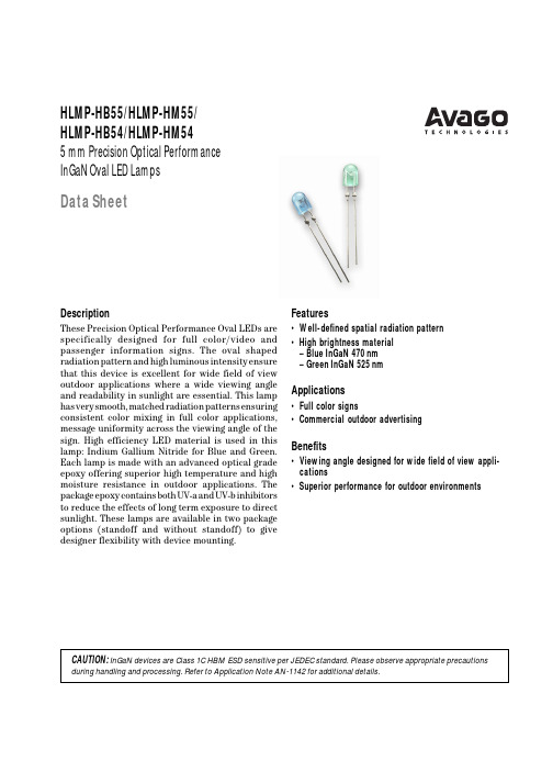
DescriptionThese Precision Optical Performance Oval LEDs are specifically designed for full color/video and passenger information signs. The oval shaped radiation pattern and high luminous intensity ensure that this device is excellent for wide field of view outdoor applications where a wide viewing angle and readability in sunlight are essential. This lamp has very smooth, matched radiation patterns ensuring consistent color mixing in full color applications, message uniformity across the viewing angle of the sign. High efficiency LED material is used in this lamp: Indium Gallium Nitride for Blue and Green. Each lamp is made with an advanced optical grade epoxy offering superior high temperature and high moisture resistance in outdoor applications. The package epoxy contains both UV-a and UV-b inhibitors to reduce the effects of long term exposure to direct sunlight. These lamps are available in two package options (standoff and without standoff) to give designer flexibility with device mounting.Features•Well-defined spatial radiation pattern•High brightness material– Blue InGaN 470 nm– Green InGaN 525 nmApplications•Full color signs•Commercial outdoor advertisingBenefits•Viewing angle designed for wide field of view appli-cations•Superior performance for outdoor environmentsHLMP-HB55/HLMP-HM55/HLMP-HB54/HLMP-HM545 mm Precision Optical PerformanceInGaN Oval LED LampsData SheetCAUTION: InGaN devices are Class 1C HBM ESD sensitive per JEDEC standard. Please observe appropriate precautions during handling and processing. Refer to Application Note AN-1142 for additional details.Package DimensionsPackage Drawing ANOTE: MEASURED JUST ABOVE FLANGE.NOTES:1. DIMENSIONS IN MILLIMETERS (INCHES).2. TOLERANCE ± 0.25 mm UNLESS OTHERWISE NOTED.Package Drawing BNOTE: MEASURED JUST ABOVE FLANGE.NOTES:1. DIMENSIONS IN MILLIMETERS (INCHES).2. TOLERANCE ± 0.25 mm UNLESS OTHERWISE NOTED.Device Selection GuideColor and Luminous LuminousDominant Intensity Iv Intensity IvWavelength λd(mcd) at(mcd) at Leads with Package Tinting Part Number(nm) Typ.20 mA Min.20 mA Max.Standoff Drawing Type HLMP-HB54-FJ0xx Blue 470110310No A Blue HLMP-HB55-HJCxx Blue 470180310Yes B Blue HLMP-HB55-JKCxx Blue 470240400Yes B Blue HLMP-HM54-MQ0xx Green 5255201500No A Green HLMP-HM55-MQ0xx Green 5255201500Yes B Green HLMP-HM55-NPCxx Green 5256801150Yes B Green HLMP-HM55-PQCxx Green 5258801500Yes B Green Notes:1The luminous intensity is measured on the mechanical axis of the lamp package.2.The optical axis is closely aligned with the package mechanical axis.3.The dominant wavelength, λd, is derived from the Chromaticity Diagram and represents the color of the lamp.Part Numbering SystemHLMP-X X XX–X X X XXMechanical Options00: Bulk PackagingDD: Ammo PackColor Bin Selections0: No color bin limitationMaximum Intensity Bin0: No Iv bin limitationMinimum Intensity BinRefer to Device Selection GuideColorB: 470 nm BlueM: 525 nm GreenPackageH: 5 mm Oval 40° x 100°Absolute Maximum Ratings at T A = 25°CParameter ValueDC Forward Current[1]30 mAPeak Pulsed Forward Current[2]100 mAPower Dissipation117 mWReverse Voltage 5 V (I R = 10 µA)LED Junction Temperature130°COperating Temperature Range–40°C to +80°CStorage Temperature Range–40°C to +100°CNotes:1. Derate linearly as shown in Figure 3.2. Duty factor 10%, Frequency 1kHzElectrical /Optical Characteristics TableT A = 25°CParameter Symbol Min.Typ.Max. Units Test ConditionsForward VoltageBlue (λd = 470 nm)V F 3.2 3.7V I F = 20 mAGreen (λd = 525 nm) 3.2 3.9Reverse Voltage V R5I R = 10 µACapacitanceBlue (λd = 470 nm)C40pF V F = 0, f = 1 MHzGreen (λd = 525 nm)Thermal Resistance RθJ-PIN240°C/W LED Junction-to-Cathode Lead Viewing AngleMajor Axis2θ1/2100degMinor Axis40Peak WavelengthBlue (λd = 470 nm)λP467nm Peak of Wavelength of Spectral Green (λd = 525 nm)520Distribution at I F = 20 mASpectral HalfwidthBlue (λd = 470 nm)∆λ1/224nm Wavelength Width at Spectral Green (λd = 525 nm)35Distribution Power Point at I F = 20 mA Luminous EfficacyBlue (λd = 470 nm)ηv75lm/W Emitted luminous power/Emitted Green (λd = 525 nm)520radiant powerNotes:1.2θ1/2 is the off-axis angle where the luminous intensity is 1/2 the on axis intensity.2.The radiant intensity, Ie in watts per steradian, may be found from the equation Ie = Iv/ηv where Iv is the luminous intensity in candelas and ηvis the luminous efficacy in lumens/watt.Figure 1. Relative intensity vs. wavelength.Figure 2. Relative luminous intensity vs.forward current.Figure 3. Forward current vs. ambient temperature.WAVELENGTH – nmR E L A T I V E L U M I N O U S I N T E N S I T Y1.00.200.40.60.8R E L A T I V E L U M I N O U S I N T E N S I T Y (N O R M A L I Z E D A T 20 m A )0FORWARD CURRENT – mA15251.20.6300.20.81.42051.00.410Figure 4. Forward current vs. forward voltage.Figure 5. Relative dominant wavelength vs.forward current.0.9851.0251.000R E L A T I V E D O M I N A N T W A V E L E N G T HFORWARD CURRENT – mA0.9901.0101.0351.0150.9951.0051.0201.030M A X I M U M F O R W A R D C U R R E N T – m A0AMBIENT TEMPERATURE – °C306025201510510508035902040703002510F O R W A R D C U R R E N T – m AFORWARD VOLTAGE – V 0 1.5 2.0 2.551530 1.00.520 3.0 3.5 4.0Figure 6. Spatial radiation pattern – minor axis.Figure 7. Spatial radiation pattern – major axis.Intensity Bin Limits (mcd @ 20 mA)Bin Name Min.Max.F 110140G 140180H 180240J 240310K 310400L 400520M 520680N 680880P 8801150Q 11501500R15001900Tolerance will be ±15% of these limits.R E L A T I V E I N T E N S I T Y1.00ANGLE – DEGREES-900.5-30105090-1030-7070-50R E L A T I V E I N T E N S I T Y1.00ANGLE – DEGREES-900.5-30105090-1030-7070-50Green Color Bin TableBin Min. Dom.Max. Dom.Xmin.Ymin.Xmax.Ymax.1520.0524.00.07430.83380.18560.65560.16500.65860.10600.82922524.0528.00.10600.82920.20680.64630.18560.65560.13870.81483528.0532.00.13870.81480.22730.63440.20680.64630.17020.79654532.0536.00.17020.79650.24690.62130.22730.63440.20030.77645536.0540.00.20030.77640.26590.60700.24690.62130.22960.7543Tolerance for each bin limit is ± 0.5 nmNote:1.All bin categories are established for classification of products. Products may not be available in all bin categories. Please contact your Avago representative for further information.Blue Color Bin TableBin Min. Dom.Max. Dom.Xmin.Ymin.Xmax.Ymax.1460.0464.00.14400.02970.17660.09660.18180.09040.13740.03742464.0468.00.13740.03740.16990.10620.17660.09660.12910.04953468.0472.00.12910.04950.16160.12090.16990.10620.11870.06714472.0476.00.11870.06710.15170.14230.16160.12090.10630.09455476.0480.00.10630.09450.13970.17280.15170.14230.09130.1327Tolerance for each bin limit is ± 0.5 nmAvago Color Bin on CIE Chromaticity DiagramPrecautions:Lead Forming•The leads of an LED lamp may be preformed or cut to length prior to insertion and soldering into PC board.•If lead forming is required before soldering, care must be taken to avoid any excessive mechanical stress induced to LED package. Otherwise, cut the leads of LED to length after soldering process at room temperature. The solder joint formed will absorb the mechanical stress of the lead cutting from traveling to the LED chip die attach and wirebond.•For better control, it is recommended to use proper tool to precisely form and cut the leads to applicable length rather than doing it manually.Soldering Conditions•Care must be taken during PCB assembly and soldering process to prevent damage to LED component.•The closest LED is allowed to solder on board is 1.59 mm below the body (encapsulant epoxy) for those parts without standoff.•Recommended soldering conditions:•Wave soldering parameter must be set and maintained according to recommended temperature and dwell time in the solder wave. Customer is advised to periodically check on the soldering profile to ensure the soldering profile used is always conforming to recommended soldering condition.Notes:1.PCB with different size and design (component density)will have different heat mass (heat capacity). This might cause a change in temperature experienced by the board if same wave soldering setting is used. So, it is recommended to recalibrate the soldering profile again before loading a new type of PCB.2.Avago Technologies' high brightness LED are using high efficiency LED die with single wire bond as shown below.Customer is advised to take extra precaution during wave soldering to ensure that the maximum wave temperature is not exceeding 250°C. Overstressing the LED during soldering process might cause premature failure to the LED due to delamination.Manual Solder Wave Soldering Dipping Pre-heat Temperature 105 °C Max.–Pre-heat Time 30 sec Max.–Peak Temperature 250 °C Max.260 °C Max.Dwell Time3 sec Max.5 sec Max.Relative Light Output vs. Junction Temperature01.0R E L A T I V E L I G H T O U T P U T (N O R M A L I Z E D A T T J = 25°C )T J – JUNCTION TEMPERATURE – °C1.20.80.20.40.6Note: Refer to application note AN1027 for more information on soldering LED components.LED Component Plated Through Lead SizeDiagonal Hole Diameter 0.457 x 0.457 mm 0.646 mm 0.976 to 1.078 mm (0.018 x 0.018 inch)(0.025 inch)(0.038 to 0.042 inch)0.508 x 0.508 mm 0.718 mm 1.049 to 1.150 mm (0.020 x 0.020 inch)(0.028 inch)(0.041 to 0.045 inch)Avago Technologies LED ConfigurationNote: Electrical connection between bottom surface of LED die and the lead frame material through conductive paste of solder.•If necessary, use fixture to hold the LED component in proper orientation with respect to the PCB during soldering process.•At elevated temperature, the LED is more susceptible to mechanical stress. Therefore, PCB must be allowed to cool down to room temperature prior to handling, which includes removal of jigs,fixtures or pallet.•Special attention must be given to board fabrication,solder masking, surface platting and lead holes size and component orientation to assure the solderability.•Over sizing of plated through hole can lead to twisting or improper LED placement during auto insertion. Under sizing plated through hole can lead to mechanical stress on the epoxy lens during clinching.•Recommended PC board plated through hole sizes for LED component leads:Figure 8. Recommended wave soldering profile.BOTTOM SIDE OF PC BOARD3050100150200250TIME – SECONDST E M P E R A T U R E – °CTOP SIDE OF PC BOARD CONVEYOR SPEED = 1.83 M/MIN (6 FT/MIN)PREHEAT SETTING = 150°C (100°C PCB)SOLDER WAVE TEMPERATURE = 245°C ± 5°C AIR KNIFE AIR TEMPERATURE = 390°C AIR KNIFE DISTANCE = 1.91 mm (0.25 IN.)AIR KNIFE ANGLE = 40°LEAD SOLDER: SN63; FLUX: RMALEAD FREE SOLDER: 96.5% Sn, 3.0% Ag, 0.5% Cu NOTE: ALLOW FOR BOARDS TO BE SUFFICIENTLY COOLED BEFORE EXERTING MECHANICAL FORCE.Ammo Packs DrawingALL DIMENSIONS IN MILLIMETERS (INCHES).Note: The ammo-packs drawing is applicable for packaging option -DD & -ZZ and regardless of standoff or non-standoff. Packaging Box Ammo PacksNote: For InGaN device, the ammo pack packaging box contains ESD logo.DISCLAIMERAVAGO’S PRODUCTS AND SOFTWARE ARE NOT SPECIFICALLY DESIGNED, MANUFACTURED OR AUTHORIZED FOR SALE AS PARTS, COMPONENTS OR ASSEMBLIES FOR THE PLANNING, CONSTRUCTION, MAINTENANCE OR DIRECT OPERATION OF A NUCLEAR FACILITY OR FOR USE IN MEDICAL DEVICES OR APPLICATIONS. CUSTOMER IS SOLELY RESPONSIBLE, AND WAIVES ALL RIGHTS TO MAKE CLAIMS AGAINST AVAGO OR ITS SUPPLIERS, FOR ALL LOSS, DAMAGE, EXPENSE OR LIABILITY IN CONNECTION WITH SUCH USE.For product information and a complete list of distributors, please go to our website: Avago, Avago Technologies, and the A logo are trademarks of Avago Technologies Limited in the United States and other countries.Data subject to change. Copyright © 2007 Avago Technologies Limited. All rights reserved. Obsoletes 5989-4145ENAV02-0206EN March 20, 2007。
HLMP-C517-X0000中文资料
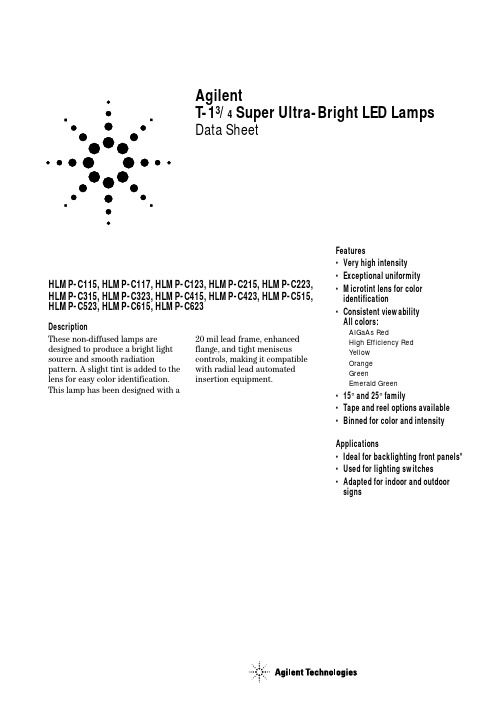
DescriptionThese non-diffused lamps are designed to produce a bright light source and smooth radiationpattern. A slight tint is added to the lens for easy color identification.This lamp has been designed with aHLMP-C115, HLMP-C117, HLMP-C123, HLMP-C215, HLMP-C223,HLMP-C315, HLMP-C323, HLMP-C415, HLMP-C423, HLMP-C515,HLMP-C523, HLMP-C615, HLMP-C623Features•Very high intensity •Exceptional uniformity •Microtint lens for color identification•Consistent viewability All colors: AlGaAs RedHigh Efficiency Red Yellow Orange GreenEmerald Green •15° and 25° family•Tape and reel options available •Binned for color and intensity Applications•Ideal for backlighting front panels*•Used for lighting switches •Adapted for indoor and outdoor signsAgilentT-13/4 Super Ultra-Bright LED LampsData Sheet20mil lead frame, enhanced flange, and tight meniscus controls, making it compatible with radial lead automated insertion equipment.Selection GuidePart Number Luminous Intensity Iv (mcd) Color2θ1/2[1]Standoff Leads HLMP-Min.Max.DH AS AlGaAs15No C115290.0–C115-O00xx290.0–C115-OP0xx290.01000.0Yes C117-OP0xx290.01000.025No C12390.2–C123-L00xx90.2–Red15No C215138.0–C215-M00xx138.0–C215-MN0xx138.0400.025No C22390.2–C223-L00xx90.2–C223-MN0xx138.0400.0 Yellow15No C315147.0–C315-L00xx147.0–C315-LM0xx147.0424.025No C32396.2–C323-K00xx96.2–C323-KL0xx96.2294.0 Orange15No C415138.0–C415-M00xx138.0–C415-M0D0xx138.0–C415-MN0xx138.0400.025No C42390.2–C423-L00xx90.2–C423-LM0xx90.2276.0 Green15No C515170.0–C515-L00xx170.0C515-LM0xx170.0490.025No C52369.8–C523-J00xx69.8–C523-KL0xx111.7340.0 Emerald Green15No C61517.0–C615-G00xx17.0–25No C623 6.7–C623-E00xx 6.7–Part Numbering SystemHLMP - C x xx - x x x xxMechanical Options00: Bulk01: Tape & Reel, Crimped Leads02: Tape & Reel, Straight LeadsB2: Right Angle Housing, Even LeadsUQ: Ammo Pack, Horizontal LeadsColor Bin Options0: Full Color Bin DistributionD: Color Bins 4 & 5 onlyMaximum Iv Bin Options0: Open (No Maximum Limit)Others: Please refer to the Iv Bin TableMinimum Iv Bin OptionsPlease refer to the Iv Bin TableViewing Angle & Standoffs Options15: 15 Degree, without Standoffs17: 15 Degree, with Standoffs23: 25 Degree, without StandoffsColor Options1. AS AlGaAs Red2. High Efficiency Red3. Yellow4. Orange5. Green6. Emerald GreenPackage OptionsC: T-1 3/4 (5 mm)Absolute Maximum Ratings at T A = 25°CHighHighDH AS Efficiency Performance AlGaAs Red and Green and ParameterRed Orange Yellow Emerald Green Units DC Forward Current [1]30302030mA Transient Forward Current [2]500500500500mA (10 µsec Pulse)Reverse Voltage (Ir = 100 µA)5555V LED Junction Temperature 110110110110°C Operating Temperature Range –20 to +100–55 to +100–20 to +100°C Storage Temperature Range –55 to +100°CWave Soldering Temperature 250°C for 3 seconds [1.59 mm (0.063 in.) from body]Lead Solder Dipping Temperature 260°C for 5 seconds[1.59 mm (0.063 in.) from body]Notes:1. See Figure 5 for maximum current derating vs. ambient temperature.2. The transient current is the maximum nonrecurring peak current the device can withstand without damaging the LED die and wire bond.Package DimensionsHLMP-Cx15 and HLMP-Cx23HLMP-Cx17(0.039)NOTES:1. ALL DIMENSIONS ARE IN MILLIMETERS (INCHES).2. LEADS ARE MILD STEEL, SOLDER DIPPED.3. AN EPOXY MENISCUS MAY EXTEND ABOUT 0.5 mm (0.020 in.) DOWN THE LEADS.± 0.20± 0.008)Electrical Characteristics at T A = 25°CForward Reverse Capacitance Speed of ResponseVoltage Breakdown C (pF)Thermalτs (ns)Vf (Volts)Vr (Volts)Vf = 0Resistance Time Constant@ If = 20 mA@ Ir = 100 µA f = 1 MHz RθJ-PIN e-t/τsPart Number Typ.Max.Min.Typ.(°C/W)Typ.HLMP-C115 1.8 2.253021030HLMP-C117HLMP-C123HLMP-C215 1.9 2.651121090HLMP-C223HLMP-C315 2.1 2.651521090HLMP-C323HLMP-C415 1.9 2.654210280HLMP-C423HLMP-C515 2.2 3.0518210260HLMP-C523HLMP-C615 2.2 3.0518210260HLMP-C623Optical Characteristics at T A = 25°CLuminous Color,ViewingIntensity Peak Dominant Angle LuminousIv (mcd)Wavelength Wavelength2θ1/2Efficacy@ 20 mA[1]λpeak (nm)λd[2] (nm)(Degrees)[3]ηvPart Number Min.Typ.Typ.Typ.Typ.(lm/w) HLMP-C1152906006456371180HLMP-C117HLMP-C1239020026HLMP-C215138300635626171459017023HLMP-C315146300583585175009617025HLMP-C415138300600602173809017023HLMP-C515170300568570205956917028HLMP-C61517455585602065662728Notes:1. The luminous intensity, Iv, is measured at the mechanical axis of the lamp package. The actual peak of the spatial radiation pattern may not bealigned with this axis.2. The dominant wavelength, λd, is derived from the CIE Chromaticity Diagram and represents the color of the device.3. 2θ1/2 is the off-axis angle where the luminous intensity is 1/2 the on-axis intensity.Figure 1. Relative intensity vs. wavelength.Figure 2. Forward current vs. forward voltage (non-resistor lamp).Figure 3. Relative luminous intensity vs. forward current.WAVELENGTH – nmR E L A T I V E I N T E N S I T Y1.00.50I F – F O R W A R DC U R R E N T – m AV F – FORWARD VOLTAGE – VI F – F O R W A R D C U R R E N T – m AV F – FORWARD VOLTAGE – VHIGH EFFICIENCY RED, ORANGE,YELLOW, AND HIGH PERFORMANCEGREEN, EMERALD GREENR E L A T I V E L U M I N O U S I N TE N S I T Y (N O R M A L I Z E D A T 20 m A )I F – DC FORWARD CURRENT – mA R E L A T I V E L U M I N O U S I N T E N S I T Y (N O R M A L I Z E D A T 20 m A )0I DC – DC CURRENT PER LED – mA10201.60.80.4515301.2250.20.61.01.4HER, ORANGE, YELLOW, AND HIGH PERFORMANCE GREEN, EMERALD GREENFigure 5. Maximum forward dc current vs. ambient temperature. Derating based on T j MAX = 110°C.Figure 4. Relative efficiency (luminous intensity per unit current) vs. peak current.Figure 6. Relative luminous intensity vs. angular displacement. 15 degree family.R E L A T I V E E F F I C I E N C Y (N O R M A L I Z E D A T 20 m A )0I PEAK – PEAK FORWARD CURRENT – mA0.60.8300201001.21.00.20.45020010DH As AlGaAs REDηP E A K – R E L A T I V E E F F I C I E N C Y (N O R M A L I Z E D A T 20 m A )I PEAK – PEAK FORWARD CURRENT – mAHER, ORANGE, YELLOW, HIGHPERFORMANCE GREEN, EMERALD GREENI F – F O R W A R D C U R R E NT – m AT A – AMBIENT TEMPERATURE – °C DH As AlGaAs REDI F – F O R W A R D C U R R E N T – m AT A – AMBIENT TEMPERATURE – °CHER, ORANGE, YELLOW, AND HIGH PERFORMANCE GREEN, EMERALD GREEN N O R M A L I Z E D L U M I N O U S I N T E N S I T Y10ANGULAR DISPLACEMENT – DEGREES0.80.60.50.70.2450.10.30.4403530252010515-5-10-15-20-25-30-35-40-450.9Figure 7. Relative luminous intensity vs. angular displacement. 25 degree family.Intensity Bin Limits Intensity Range (mcd)ColorBin Min.Max.L 101.5162.4M 162.4234.6N 234.6340.0O 340.0540.0P 540.0850.0Q 850.01200.0R 1200.01700.0Red/OrangeS 1700.02400.0T 2400.03400.0U 3400.04900.0V 4900.07100.0W 7100.010200.0X 10200.014800.0Y 14800.021400.0Z 21400.030900.0L 173.2250.0M 250.0360.0N 360.0510.0O 510.0800.0P 800.01250.0YellowQ 1250.01800.0R 1800.02900.0S 2900.04700.0T 4700.07200.0U 7200.011700.0V 11700.018000.0W18000.027000.0N O R M A L I Z E D L U M I N O U S I N T E N S I T Y10ANGULAR DISPLACEMENT – DEGREES0.80.60.50.70.2450.10.30.4403530252010515-5-10-15-20-25-30-35-40-450.9Intensity Bin Limits, continuedIntensity Range (mcd) Color Bin Min.Max.E7.612.0F12.019.1G19.130.7H30.749.1I49.178.5J78.5125.7K125.7201.1L201.1289.0 Green/M289.0417.0 Emerald Green N417.0680.0O680.01100.0P1100.01800.0Q1800.02700.0R2700.04300.0S4300.06800.0T6800.010800.0U10800.016000.0V16000.025000.0W25000.040000.0 Maximum tolerance for each bin limit is ± 18%.Color CategoriesLambda (nm)Color Category #Min.Max.6561.5564.55564.5567.5 Green4567.5570.53570.5573.52573.5576.51582.0584.53584.5587.0 Yellow2587.0589.54589.5592.05592.0593.01597.0599.52599.5602.03602.0604.5 Orange4604.5607.55607.5610.56610.5613.57613.5616.58616.5619.5 Tolerance for each bin limit is ± 0.5 nm.Mechanical Option MatrixMechanical Option Code Definition00Bulk Packaging, minimum increment 500 pcs/bag01Tape & Reel, crimped leads, minimum increment 1300 pcs/bag02Tape & Reel, straight leads, minimum increment 1300 pcs/bagB2Right Angle Housing, even leads, minimum increment 500 pcs/bagUQ Ammo Pack, horizontal leads, in 1K minimum incrementNote:All categories are established for classification of products. Products may not be available in all categories. Please contact your local Agilent representative for further clarification/information./semiconductorsFor product information and a complete list ofdistributors, please go to our web site.For technical assistance call:Americas/Canada: +1 (800) 235-0312 or(916) 788-6763Europe: +49 (0) 6441 92460China: 10800 650 0017Hong Kong: (+65) 6756 2394India, Australia, New Zealand: (+65) 6755 1939Japan: (+81 3) 3335-8152 (Domestic/Interna-tional), or 0120-61-1280 (Domestic Only)Korea: (+65) 6755 1989Singapore, Malaysia, Vietnam, Thailand,Philippines, Indonesia: (+65) 6755 2044Taiwan: (+65) 6755 1843Data subject to change.Copyright © 2004 Agilent Technologies, Inc.Obsoletes 5965-6165ENovember 11, 20045988-2149EN。
abb工业机器人协同动作应用手册

Robotics Products Se-721 68 Västerås
瑞典
目表
目表
手册概述 ............................................................................................................................................. 7 产品文档,IRC5 ................................................................................................................................. 9 安全 .................................................................................................................................................... 11
应用手册 MultiMove
Trace back information: Workspace R15-2 version a20 Checked in 2015-10-22 Skribenta version 4.6.176
应用手册 MultiMove
RobotWare 6.02 文档编号: 3HAC050961-010
3.2.1 Controller参数域集合 ................................................................................ 30 3.2.2 Motion参数域集合 .................................................................................... 32 3.2.3 I/O参数域集合 ......................................................................................... 33 3.3 配置示例 .......................................................................................................... 34 3.3.1 “UnsyncArc”的配置示例 ............................................................................ 34 3.3.2 “SyncArc”的配置示例 ............................................................................... 36 3.3.3 输入/输出配置示例 ................................................................................... 38
HLMP-CB11中文资料

Agilent HLMP-CxxxT-13/4 (5mm) Extra Bright Precision Optical Performance InGaN LED Lamps Data SheetDescriptionThese high intensity blue and green LEDs are based on the most efficient and cost effective InGaN material technology. The 470 nm typical dominant wave–length for blue and 525 nm typical wavelength for green is well suited to color mixing in full color signs. The 505 nm typical dominant wavelength for cyan is suitable for traffic signal application.These LED lamps are untinted, non-diffused, T-13/4 packagesFeatures•Well defined spatial radiationpattern•High luminous output•Available in blue, green, and cyancolor•Viewing angle: 15°, 23°and 30°•Standoff or non-standoff leads•Superior resistance to moistureApplications•Traffic signals•Commercial outdoor advertising•Front panel backlighting•Front panel indicator incorporating second generationoptics which produce well-definedspatial radiation patterns atspecific viewing cone angles.These lamps are made with anadvanced optical grade epoxy,offering superior temperatureand moisture resistance inoutdoor signal and signapplications. The high maximumLED junction temperature limitof +110°C enables hightemperature operation in brightsunlight conditions.HLMP-CB11, HLMP-CB12, HLMP-CM11, HLMP-CM12, HLMP-CE11,HLMP-CE12, HLMP-CB26, HLMP-CB27, HLMP-CM26, HLMP-CM27,HLMP-CE26, HLMP-CE27, HLMP-CB36, HLMP-CB37, HLMP-CM36,HLMP-CM37, HLMP-CE36, HLMP-CE37CAUTION: Devices are Class I ESD sensitive. Please observe appropriate precautions during handling and processing. Refer to Application Note AN-1142 for additional details.Package DimensionsPackage APackage B5.80 ± 0.20(0.228 ±∅ CATHODEFLATMIN.SQ. TYP.NOTES:1. MEASURED JUST ABOVE FLANGE.2. ALL DIMENSIONS ARE IN MILLIMETERS (INCHES).3. EPOXY MENISCUS MAY EXTEND ABOUT 1 mm (0.040") DOWN THE LEADS.4. IF HEAT SINKING APPLICATION IS REQUIRED, THE TERMINAL FOR HEAT SINK IS ANODE.Device Selection GuideTypicalViewing Angle,Intensity (cd) at 20 mA PackagePart Number Color2q1/2 (Degree)Min.Max.Standoff Dimension Lens HLMP-CB11-TW0xx Blue15 2.57.2No A Clear HLMP-CB11-UVAxx Blue15 3.2 5.5No A Clear HLMP-CB12-TW0xx Blue15 2.57.2Yes B Clear HLMP-CM11-Y20xx Green159.327.0No A Clear HLMP-CM11-Z1Cxx Green1512.021.0No A Clear HLMP-CM12-Y20xx Green159.327.0Yes B Clear HLMP-CE11-X10xx Cyan157.221.0No A Clear HLMP-CE12-X10xx Cyan157.221.0Yes B Clear HLMP-CB26-SV0xx Blue23 1.9 5.5No A Clear HLMP-CB26-TUDxx Blue23 2.5 4.2No A Clear HLMP-CB27-SV0xx Blue23 1.9 5.5Yes B Clear HLMP-CM26-X10xx Green237.221.0No A Clear HLMP-CM26-YZCxx Green239.316.0No A Clear HLMP-CM27-X10xx Green237.221.0Yes B Clear HLMP-CE26-WZ0xx Cyan23 5.516.0No A Clear HLMP-CE27-WZ0xx Cyan23 5.516.0Yes B Clear HLMP-CB36-QT0xx Blue30 1.15 3.2No A Clear HLMP-CB36-RSAxx Blue30 1.5 2.5No A Clear HLMP-CB37-RU0xx Blue30 1.5 4.2Yes B Clear HLMP-CB37-RSDxx Blue30 1.5 2.5Yes B Clear HLMP-CM36-X10xx Green307.221.0No A Clear HLMP-CM36-XYCxx Green307.212.0No A Clear HLMP-CM37-X10xx Green307.221.0Yes B Clear HLMP-CM37-XYCxx Green307.212.0Yes B Clear HLMP-CM37-XYDxx Green307.212.0Yes B Clear HLMP-CE36-WZ0xx Cyan30 5.516.0No A Clear HLMP-CE37-WZ0xx Cyan30 5.516.0Yes B ClearNotes:1.Tolerance for luminous intensity measurement is ±15%.2.The luminous intensity is measured on the mechanical axis of the lamp package.3.The optical axis is closely aligned with the package mechanical axis.4.LED light output is bright enough to cause injuries to the eyes. Precautions must be taken to prevent looking directly at the LED without propersafety equipment.5. 2q1/2 is the off-axis angle where the luminous intensity is 1/2 the on-axis intensity.Part Numbering SystemHLMP-x x xx-x x x xxMechanical Options00: BulkDD: Ammo PackColor Bin Options0: Full Color Bin DistributionA: Color Bin 1 and 2C: Color Bin 3 and 4D: Color Bin 4 and 5Maximum Intensity Bin0: No Maximum Intensity Bin LimitationOthers: Refer to Device Selection GuideMinimum Intensity BinRefer to Device Selection GuideViewing Intensity Bin11: 15° Without Standoff12: 15°With Standoff26: 23°Without Standoff27: 23°With Standoff36: 30°Without standoff37: 30°With StandoffColorB: Blue 470 nmM: Green 525 nmE: Cyan 505 nmPackageC: T-13/4 (5 mm) Round LampAbsolute Maximum Rating at T A = 25°CParameters Value UnitDC Forward Current [1]30mAPeak Pulsed Forward Current[3]100mAAverage Forward Current30mAPower Dissipation120mWLED Junction Temperature110°COperating Temperature Range–40 to +85°CStorage Temperature Range–40 to +100°CWave Soldering Temperature[2]250 for 3 secs°CNotes:1.Derate linearly as shown in Figure2.2.1.59 mm (0.060 inch) below body.3.Duty factor 10%, frequency 1 KHz.Electrical/Optical CharacteristicsT A = 25o CBlue Green CyanParameters Symbol Min.Typ.Max.Min.Typ.Max.Min.Typ.Max.Units Test Condition Forward Voltage V F 3.5 4.0 3.6 4.0 3.5 4.0V I F = 20 mA Reverse Voltage[1]V R 5.0 5.0 5.0V I R = 10 µA Thermal Resistance R q J-PIN240240240o C/W LED Junction toAnode Lead Dominant l d460470480520525540490505510nm I F = 20 mA Wavelength[2]Peak Wavelength l PEAK464516501nm Peak of Wavelengthof Spectral Distribu-tion at I F = 20 mA Spectral Half Width Dl1/2233230nm Wavelength Widthat Spectral Distribu-tion Power Pointat I F = 20 mA Luminous Efficacy[3]h v74484319lm/W Emitted LuminousPower/EmittedRadiant Power Notes:1.The reverse voltage of the product is equivalent to the forward voltage of the protective chip at I R = 10 µA.2.The dominant wavelength, l d, is derived from the Chromaticity Diagram and represents the color of the lamp.3.The radiant intensity, Ie in watts/steradian, may be found from the equation Ie = Iv/h v, where Iv is the luminous intensity in candelas and h v is theluminous efficacy in lumens/watt.Figure 5. Relative intensity vs. DC forward current.Figure 4. Relative dominant wavelength vs. DC forward current.DC FORWARD CURRENT – mAR E L A T I V E D O M I N A N T W A V E L E N G T H (N O R M A L I Z E D A T 20 m A )1020301.0250.9901.0151.0201.0101.0051.0000.995GREENBLUER E L A T I V E I N T E N S I T Y (N O R M A L I Z E D A T 20 m A )FORWARD CURRENT – mAFigure 1. Relative intensity vs. wavelength.Figure 3. Forward current vs. forward voltage.Figure 2. Forward current vs. ambient temperature.WAVELENGTH – nmR E L A T I V E I N T E N S I T Y1.0000.800.600.400.20030103.0202.01.0F O R W A R D C U R R E N T – m AFORWARD VOLTAGE – V 4.0CYANGREENBLUEI F – F O R W A R D C U R R E N T – m AV F – FORWARD VOLTAGE – VOLTSFigure 6. Spatial radiation pattern for Cx11 and Cx12.R E L A T I V E L U M I N O U S I N T E N S I T Y10ANGULAR DISPLACEMENT – DEGREES0.5-90-600-30306090Figure 7. Spatial radiation pattern for Cx26 and Cx27.Figure 8. Spatial radiation pattern for Cx36 and Cx37.R E L A T I V E L U M I N O U S I N T E N S I T Y10ANGULAR DISPLACEMENT – DEGREES0.5-90-600-30306090R E L A T I V E L U M I N O U S I N T E N S I T Y10ANGULAR DISPLACEMENT – DEGREES0.5-90-600-30306090Intensity Bin Limit TableIntensity (mcd) at 20 mA Bin Min MaxN680880P8801150Q11501500R15001900S1*******T25003200U32004200V42005500W55007200X72009300Y930012000Z1200016000 11600021000 Tolerance for each bin limit is ±15%.Blue Color Bin TableBin Min Dom Max Dom Xmin Ymin Xmax Ymax 1460.0464.00.14400.02970.17660.09660.18180.09040.13740.0374 2464.0468.00.13740.03740.16990.10620.17660.09660.12910.0495 3468.0472.00.12910.04950.16160.12090.16990.10620.11870.0671 4472.0476.00.11870.06710.15170.14230.16160.12090.10630.0945 5476.0480.00.10630.09450.13970.17280.15170.14230.09130.1327 Tolerance for each bin limit is ±0.5 nm.Cyan Color Bin TableBin Min Dom Max Dom Xmin Ymin Xmax Ymax 1490.0495.00.04540.29450.11640.38890.13180.3060.02350.4127 2495.0500.00.03450.41270.10570.47690.11640.38890.00820.5384 3500.0505.00.00820.53840.10270.55840.10570.47690.00390.6548 4505.0510.00.00390.65480.10970.62510.10270.55840.01390.7502 7498.0503.00.01320.48820.10280.52730.10920.44170.00400.6104 8503.0508.00.00400.61040.10560.60070.10280.52730.00800.7153 Tolerance for each bin limit is ±0.5 nm.Green Color Bin TableBin Min Dom Max Dom Xmin Ymin Xmax Ymax 1520.0524.00.07430.83380.18560.65560.16500.65860.10600.8292 2524.0528.00.10600.82920.20680.64630.18560.65560.13870.8148 3528.0532.00.13870.81480.22730.63440.20680.64630.17020.7965 4532.0536.00.17020.79650.24690.62130.22730.63440.20030.7764 5536.0540.00.20030.77640.26590.60700.24690.62130.22960.7543 Tolerance for each bin limit is ±0.5 nm./semiconductors For product information and a complete list of distributors, please go to our web site.For technical assistance call:Americas/Canada: +1 (800) 235-0312 or (916) 788-6763Europe: +49 (0) 6441 92460China: 10800 650 0017Hong Kong: (+65) 6756 2394India, Australia, New Zealand: (+65) 6755 1939 Japan: (+81 3) 3335-8152(Domestic/Interna-tional), or 0120-61-1280(Domestic Only) Korea: (+65) 6755 1989Singapore, Malaysia, Vietnam, Thailand, Philippines, Indonesia: (+65) 6755 2044 Taiwan: (+65) 6755 1843Data subject to change.Copyright © 2004 Agilent Technologies, Inc. December 7, 20045989-1022EN。
HLMP-K105-ML0DD中文资料
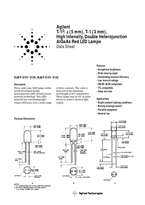
AgilentT-13/4 (5 mm), T-1 (3 mm),High Intensity, Double Heterojunction AlGaAs Red LED LampsData SheetHLMP-D101/D105, HLMP-K101/K105DescriptionThese solid state LED lamps utilize newly developed doubleheterojunction (DH) AlGaAs/GaAs material technology. This LED material has outstanding lightoutput efficiency over a wide rangeFeatures• Exceptional brightness • Wide viewing angle• Outstanding material efficiency • Low forward voltage • CMOS/MOS compatible • TTL compatible • Deep red colorApplications• Bright ambient lighting conditions • Moving message panels • Portable equipment • General useof drive currents. The color is deep red at the dominantwavelength of 637 nanometres.These lamps may be DC or pulse driven to achieve desired light output.Package DimensionsA B CSelection GuideLuminous IntensityIv (mcd) at 20 mA2θ1/2[1]Package Package Description Device HLMP-Min.Typ.Max.Degree Outline T-1 3/4 Red Tinted Diffused D10135.270.0–65AD101-J00xx35.270.0–65AD101-JK0xx35.270.0112.865AT-1 3/4 Red Untinted Non-diffused D105138.0240.0–24BD105-M00xx138.0240.0–24BD105-NO0xx200.0290.0580.024BT-1 Red Tinted Diffused K10122.045.0–60CK101-100xx22.045.0–60CK101-IJ0xx22.045.070.460CT-1 Red Untinted Non-diffused K10535.265.0–45CK105-J00xx35.265.0–45CK105-KL0xx56.4110.0180.445CNote:1. θ1/2 is the off axis angle from lamp centerline where the luminous intensity is 1/2 the on-axis value.Part Numbering SystemHLMP - x x xx - x x x xxMechanical Option00: Bulk01: Tape & Reel, Crimped Leads02: Tape & Reel, Straight LeadsA1: Right Angle Housing, Uneven Leads, T1A2: Right Angle Housing, Even Leads, T1B1: Right Angle Housing, Uneven Leads, T-1 3/4B2: Right Angle Housing, Even Leads, T-1 3/4DD, UQ: Ammo PackColor Bin Options0: Full Color Bin DistributionMaximum Iv Bin Options0: Open (no max. limit)Others: Please refer to the Iv Bin TableMinimum Iv Bin OptionsPlease refer to the Iv Bin TableLens Type01: Tinted, Diffused05: Untinted, NondiffusedColor Options1: AlGaAs RedPackage OptionsD: T-1 3/4K: T-1Absolute Maximum Ratings at T A = 25°CParameter ValuePeak Forward Current[1,2]300 mAAverage Forward Current[2]20 mADC Current[3]30 mAPower Dissipation87 mWReverse Voltage (I R = 100 µA) 5 VTransient Forward Current (10 µs Pulse)[4]500 mALED Junction Temperature110°COperating Temperature Range-20 to +100°C Storage Temperature Range-55 to +100°C Wave Soldering Temperature [1.59 mm (0.063 in.) from body]250°C for 3 seconds Lead Solder Dipping Temperature [1.59 mm (0.063 in.) from body]260°C for 5 seconds Notes:1.Maximum I PEAK at f = 1 kHz, DF = 6.7%.2.Refer to Figure 6 to establish pulsed operating conditions.3.Derate linearly as shown in Figure 5.4.The transient peak current is the maximum non-recurring peak current the device can withstand without damaging the LED die and wire bonds. It isnot recommended that the device be operated at peak currents beyond the Absolute Maximum Peak Forward Current.Electrical/Optical Characteristics at T A = 25°CSymbol Description Min.Typ.Max.Unit Test ConditionV F Forward Voltage 1.8 2.2V I F = 20 mAV R Reverse Breakdown Voltage 5.015.0V I R = 100 µAλp Peak Wavelength645nm Measurement at Peakλd Dominant Wavelength637nm Note 1∆λ1/2Spectral Line Halfwidth20nmτS Speed of Response30ns Exponential TimeConstant, e-t/T SC Capacitance30pF V F = 0, f = 1 MHzRθJ-PIN Thermal Resistance260[3]°C/W Junction to Cathode Lead210[4]290[5]ηV Luminous Efficacy80Im/W Note 2Notes:1.The dominant wavelength, λd, is derived from the CIE chromaticity diagram and represents the color of the device.2.The radiant intensity, I e, in watts per steradian, may be found from the equation I e = l V/ηV, where I V is the luminous intensity in candelas and ηV isluminous efficacy in lumens/watt.3.HLMP-D101.4.HLMP-D105.5.HLMP-K101/-K105.Figure 3. Relative luminous intensity vs. dc forward current.Figure 4. Relative efficiency vs. peak forward current.Figure 7. Relative luminous intensity vs. angular displacement. HLMP-D101.Figure 8. Relative luminous intensity vs. angular displacement. HLMP-K101.Intensity Bin LimitsIntensity Range (mcd)Color Bin Min.Max.Red I24.839.6J39.663.4K63.4101.5L101.5162.4M162.4234.6N234.6340.0O340.0540.0P540.0850.0Q850.01200.0R1200.01700.0S1700.02400.0T2400.03400.0U3400.04900.0V4900.07100.0W7100.010200.0X10200.014800.0Y14800.021400.0Z21400.030900.0Maximum tolerance for each bin limit is ± 18%.Mechanical Option MatrixMechanical Option Code Definition00Bulk Packaging, minimum increment 500 pcs/bag01Tape & Reel, crimped leads, minimum increment 1300 pcs (T-1 3/4)/1800 pcs (T-1) 02Tape & Reel, straight leads, minimum increment 1300 pcs (T-1 3/4)/1800 pcs (T-1) A1Right Angle Housing, uneven leads, minimum increment 500 pcs/bagA2Right Angle Housing, even leads, minimum increment 500 pcs/bagB1Right Angle Housing, uneven leads, minimum increment 500 pcs/bagB2Right Angle Housing, even leads, minimum increment 500 pcs/bagDD Ammo Pack, straight leads in 2K incrementUQ Ammo Pack, horizontal leads in 2K incrementNote:All categories are established for classification of products. Products may not be available in all categories. Please contact your local Agilent representative for further clarification/information./semiconductors For product information and a complete list of distributors, please go to our web site.For technical assistance call:Americas/Canada: +1 (800) 235-0312 or (916) 788-6763Europe: +49 (0) 6441 92460China: 10800 650 0017Hong Kong: (+65) 6756 2394India, Australia, New Zealand: (+65) 6755 1939 Japan: (+81 3) 3335-8152 (Domestic/Interna-tional), or 0120-61-1280 (Domestic Only) Korea: (+65) 6755 1989Singapore, Malaysia, Vietnam, Thailand, Philippines, Indonesia: (+65) 6755 2044 Taiwan: (+65) 6755 1843Data subject to change.Copyright © 2004 Agilent Technologies, Inc. Obsoletes 5968-1440ENovember 12, 20045988-2230EN。
HLMP-CB11-S0A00中文资料
Agilent HLMP-CxxxT-13/4 (5mm) Extra Bright Precision Optical Performance InGaN LED Lamps Data SheetDescriptionThese high intensity blue and green LEDs are based on the most efficient and cost effective InGaN material technology. The 470 nm typical dominant wave–length for blue and 525 nm typical wavelength for green is well suited to color mixing in full color signs. The 505 nm typical dominant wavelength for cyan is suitable for traffic signal application.These LED lamps are untinted, non-diffused, T-13/4 packagesFeatures•Well defined spatial radiationpattern•High luminous output•Available in blue, green, and cyancolor•Viewing angle: 15°, 23°and 30°•Standoff or non-standoff leads•Superior resistance to moistureApplications•Traffic signals•Commercial outdoor advertising•Front panel backlighting•Front panel indicator incorporating second generationoptics which produce well-definedspatial radiation patterns atspecific viewing cone angles.These lamps are made with anadvanced optical grade epoxy,offering superior temperatureand moisture resistance inoutdoor signal and signapplications. The high maximumLED junction temperature limitof +110°C enables hightemperature operation in brightsunlight conditions.HLMP-CB11, HLMP-CB12, HLMP-CM11, HLMP-CM12, HLMP-CE11,HLMP-CE12, HLMP-CB26, HLMP-CB27, HLMP-CM26, HLMP-CM27,HLMP-CE26, HLMP-CE27, HLMP-CB36, HLMP-CB37, HLMP-CM36,HLMP-CM37, HLMP-CE36, HLMP-CE37CAUTION: Devices are Class I ESD sensitive. Please observe appropriate precautions during handling and processing. Refer to Application Note AN-1142 for additional details.Package DimensionsPackage APackage B5.80 ± 0.20(0.228 ±∅ CATHODEFLATMIN.SQ. TYP.NOTES:1. MEASURED JUST ABOVE FLANGE.2. ALL DIMENSIONS ARE IN MILLIMETERS (INCHES).3. EPOXY MENISCUS MAY EXTEND ABOUT 1 mm (0.040") DOWN THE LEADS.4. IF HEAT SINKING APPLICATION IS REQUIRED, THE TERMINAL FOR HEAT SINK IS ANODE.Device Selection GuideTypicalViewing Angle,Intensity (cd) at 20 mA PackagePart Number Color2q1/2 (Degree)Min.Max.Standoff Dimension Lens HLMP-CB11-TW0xx Blue15 2.57.2No A Clear HLMP-CB11-UVAxx Blue15 3.2 5.5No A Clear HLMP-CB12-TW0xx Blue15 2.57.2Yes B Clear HLMP-CM11-Y20xx Green159.327.0No A Clear HLMP-CM11-Z1Cxx Green1512.021.0No A Clear HLMP-CM12-Y20xx Green159.327.0Yes B Clear HLMP-CE11-X10xx Cyan157.221.0No A Clear HLMP-CE12-X10xx Cyan157.221.0Yes B Clear HLMP-CB26-SV0xx Blue23 1.9 5.5No A Clear HLMP-CB26-TUDxx Blue23 2.5 4.2No A Clear HLMP-CB27-SV0xx Blue23 1.9 5.5Yes B Clear HLMP-CM26-X10xx Green237.221.0No A Clear HLMP-CM26-YZCxx Green239.316.0No A Clear HLMP-CM27-X10xx Green237.221.0Yes B Clear HLMP-CE26-WZ0xx Cyan23 5.516.0No A Clear HLMP-CE27-WZ0xx Cyan23 5.516.0Yes B Clear HLMP-CB36-QT0xx Blue30 1.15 3.2No A Clear HLMP-CB36-RSAxx Blue30 1.5 2.5No A Clear HLMP-CB37-RU0xx Blue30 1.5 4.2Yes B Clear HLMP-CB37-RSDxx Blue30 1.5 2.5Yes B Clear HLMP-CM36-X10xx Green307.221.0No A Clear HLMP-CM36-XYCxx Green307.212.0No A Clear HLMP-CM37-X10xx Green307.221.0Yes B Clear HLMP-CM37-XYCxx Green307.212.0Yes B Clear HLMP-CM37-XYDxx Green307.212.0Yes B Clear HLMP-CE36-WZ0xx Cyan30 5.516.0No A Clear HLMP-CE37-WZ0xx Cyan30 5.516.0Yes B ClearNotes:1.Tolerance for luminous intensity measurement is ±15%.2.The luminous intensity is measured on the mechanical axis of the lamp package.3.The optical axis is closely aligned with the package mechanical axis.4.LED light output is bright enough to cause injuries to the eyes. Precautions must be taken to prevent looking directly at the LED without propersafety equipment.5. 2q1/2 is the off-axis angle where the luminous intensity is 1/2 the on-axis intensity.Part Numbering SystemHLMP-x x xx-x x x xxMechanical Options00: BulkDD: Ammo PackColor Bin Options0: Full Color Bin DistributionA: Color Bin 1 and 2C: Color Bin 3 and 4D: Color Bin 4 and 5Maximum Intensity Bin0: No Maximum Intensity Bin LimitationOthers: Refer to Device Selection GuideMinimum Intensity BinRefer to Device Selection GuideViewing Intensity Bin11: 15° Without Standoff12: 15°With Standoff26: 23°Without Standoff27: 23°With Standoff36: 30°Without standoff37: 30°With StandoffColorB: Blue 470 nmM: Green 525 nmE: Cyan 505 nmPackageC: T-13/4 (5 mm) Round LampAbsolute Maximum Rating at T A = 25°CParameters Value UnitDC Forward Current [1]30mAPeak Pulsed Forward Current[3]100mAAverage Forward Current30mAPower Dissipation120mWLED Junction Temperature110°COperating Temperature Range–40 to +85°CStorage Temperature Range–40 to +100°CWave Soldering Temperature[2]250 for 3 secs°CNotes:1.Derate linearly as shown in Figure2.2.1.59 mm (0.060 inch) below body.3.Duty factor 10%, frequency 1 KHz.Electrical/Optical CharacteristicsT A = 25o CBlue Green CyanParameters Symbol Min.Typ.Max.Min.Typ.Max.Min.Typ.Max.Units Test Condition Forward Voltage V F 3.5 4.0 3.6 4.0 3.5 4.0V I F = 20 mA Reverse Voltage[1]V R 5.0 5.0 5.0V I R = 10 µA Thermal Resistance R q J-PIN240240240o C/W LED Junction toAnode Lead Dominant l d460470480520525540490505510nm I F = 20 mA Wavelength[2]Peak Wavelength l PEAK464516501nm Peak of Wavelengthof Spectral Distribu-tion at I F = 20 mA Spectral Half Width Dl1/2233230nm Wavelength Widthat Spectral Distribu-tion Power Pointat I F = 20 mA Luminous Efficacy[3]h v74484319lm/W Emitted LuminousPower/EmittedRadiant Power Notes:1.The reverse voltage of the product is equivalent to the forward voltage of the protective chip at I R = 10 µA.2.The dominant wavelength, l d, is derived from the Chromaticity Diagram and represents the color of the lamp.3.The radiant intensity, Ie in watts/steradian, may be found from the equation Ie = Iv/h v, where Iv is the luminous intensity in candelas and h v is theluminous efficacy in lumens/watt.Figure 5. Relative intensity vs. DC forward current.Figure 4. Relative dominant wavelength vs. DC forward current.DC FORWARD CURRENT – mAR E L A T I V E D O M I N A N T W A V E L E N G T H (N O R M A L I Z E D A T 20 m A )1020301.0250.9901.0151.0201.0101.0051.0000.995GREENBLUER E L A T I V E I N T E N S I T Y (N O R M A L I Z E D A T 20 m A )FORWARD CURRENT – mAFigure 1. Relative intensity vs. wavelength.Figure 3. Forward current vs. forward voltage.Figure 2. Forward current vs. ambient temperature.WAVELENGTH – nmR E L A T I V E I N T E N S I T Y1.0000.800.600.400.20030103.0202.01.0F O R W A R D C U R R E N T – m AFORWARD VOLTAGE – V 4.0CYANGREENBLUEI F – F O R W A R D C U R R E N T – m AV F – FORWARD VOLTAGE – VOLTSFigure 6. Spatial radiation pattern for Cx11 and Cx12.R E L A T I V E L U M I N O U S I N T E N S I T Y10ANGULAR DISPLACEMENT – DEGREES0.5-90-600-30306090Figure 7. Spatial radiation pattern for Cx26 and Cx27.Figure 8. Spatial radiation pattern for Cx36 and Cx37.R E L A T I V E L U M I N O U S I N T E N S I T Y10ANGULAR DISPLACEMENT – DEGREES0.5-90-600-30306090R E L A T I V E L U M I N O U S I N T E N S I T Y10ANGULAR DISPLACEMENT – DEGREES0.5-90-600-30306090Intensity Bin Limit TableIntensity (mcd) at 20 mA Bin Min MaxN680880P8801150Q11501500R15001900S1*******T25003200U32004200V42005500W55007200X72009300Y930012000Z1200016000 11600021000 Tolerance for each bin limit is ±15%.Blue Color Bin TableBin Min Dom Max Dom Xmin Ymin Xmax Ymax 1460.0464.00.14400.02970.17660.09660.18180.09040.13740.0374 2464.0468.00.13740.03740.16990.10620.17660.09660.12910.0495 3468.0472.00.12910.04950.16160.12090.16990.10620.11870.0671 4472.0476.00.11870.06710.15170.14230.16160.12090.10630.0945 5476.0480.00.10630.09450.13970.17280.15170.14230.09130.1327 Tolerance for each bin limit is ±0.5 nm.Cyan Color Bin TableBin Min Dom Max Dom Xmin Ymin Xmax Ymax 1490.0495.00.04540.29450.11640.38890.13180.3060.02350.4127 2495.0500.00.03450.41270.10570.47690.11640.38890.00820.5384 3500.0505.00.00820.53840.10270.55840.10570.47690.00390.6548 4505.0510.00.00390.65480.10970.62510.10270.55840.01390.7502 7498.0503.00.01320.48820.10280.52730.10920.44170.00400.6104 8503.0508.00.00400.61040.10560.60070.10280.52730.00800.7153 Tolerance for each bin limit is ±0.5 nm.Green Color Bin TableBin Min Dom Max Dom Xmin Ymin Xmax Ymax 1520.0524.00.07430.83380.18560.65560.16500.65860.10600.8292 2524.0528.00.10600.82920.20680.64630.18560.65560.13870.8148 3528.0532.00.13870.81480.22730.63440.20680.64630.17020.7965 4532.0536.00.17020.79650.24690.62130.22730.63440.20030.7764 5536.0540.00.20030.77640.26590.60700.24690.62130.22960.7543 Tolerance for each bin limit is ±0.5 nm./semiconductors For product information and a complete list of distributors, please go to our web site.For technical assistance call:Americas/Canada: +1 (800) 235-0312 or (916) 788-6763Europe: +49 (0) 6441 92460China: 10800 650 0017Hong Kong: (+65) 6756 2394India, Australia, New Zealand: (+65) 6755 1939 Japan: (+81 3) 3335-8152(Domestic/Interna-tional), or 0120-61-1280(Domestic Only) Korea: (+65) 6755 1989Singapore, Malaysia, Vietnam, Thailand, Philippines, Indonesia: (+65) 6755 2044 Taiwan: (+65) 6755 1843Data subject to change.Copyright © 2004 Agilent Technologies, Inc. December 7, 20045989-1022EN。
HLMP-7019-D0000中文资料
HLMP-Pxxx Series, HLMP-Qxxx Series HLMP-6xxx Series, HLMP-70xx SeriesAgilent HLMP-PxxxSubminiature LED LampsData SheetFeatures•Subminiature flat top package –ideal for backlighting and light piping applications•Subminiature dome package –diffused dome for wide viewing angle–nondiffused dome for high brightness•TTL and LSTTL compatible 5 volt resistor lamps•Available in six colors •Ideal for space limited applications •Axial leads•Available with lead configurations for surface mount and through hole PC board mountingDescriptionFlat Top PackageThe HLMP-Pxxx Series flat top lamps use an untinted, non-diffused, truncated lens toprovide a wide radiation pattern that is necessary for use in backlighting applications. The flat top lamps are also ideal for use as emitters in light pipe applications.Dome PackagesThe HLMP-6xxx Series dome lamps for use as indicators use a tinted, diffused lens to provide a wide viewing angle with a high on-off contrast ratio. High brightness lamps use anuntinted, nondiffused lens to provide a high luminous intensity within a narrow radiation pattern.Resistor LampsThe HLMP-6xxx Series 5 volt subminiature lamps with built in current limiting resistors are for use in applications where space is at a premium.Lead ConfigurationsAll of these devices are made by encapsulating LED chips onaxial lead frames to form molded epoxy subminiature lamppackages. A variety of package configuration options is avail-able. These include special surface mount lead configura-tions, gull wing, yoke lead or Z-bend. Right angle lead bends at 2.54 mm (0.100 inch) and 5.08mm (0.200 inch) centerspacing are available for through hole mounting. For moreinformation refer to Standard SMT and Through Hole Lead Bend Options for Subminiature LED Lamps data sheet.Device Selection GuidePart Number: HLMP-xxxxDH AS High High Device Standard AlGaAs Efficiency Perf.Emerald Outline Red Red Red Orange Yellow Green Green Device Description[1]Drawing P005P105P205P405P305P505P605Untinted, Nondiffused,AFlat TopP102P202P402P302P502Untinted, Diffused, Flat Top A6000Q1006300Q40064006500Q600Tinted, Diffused B Q1056305Q40564056505Q605Untinted, Nondiffused,BHigh BrightnessQ150700070197040Tinted, Diffused, Low Current BQ155Nondiffused, Low Current B660067006800Tinted, Diffused, Resistor,B5 V, 10 mA662067206820Diffused, Resistor, 5 V, 4 mA BOrdering InformationHLMX-XXXX-X X X X XPackagingOptionColor BinSelectionMax. Iv BinMin. Iv Bin4 x 4 Prod.PartNumber2.082.34(0.082)(0.092)STRIPE(B) Diffused and NondiffusedFigure 1. Proper right angle mounting to a PC board to prevent protruding cathode tab from shorting to anode connection.Package Dimensions (A) Flat Top LampsNO. ANODE DOWN.YES. CATHODE DOWN.NOTES:1. ALL DIMENSIONS ARE IN MILLIMETRES (INCHES).2. PROTRUDING SUPPORT TAB IS CONNECTED TO CATHODE LEAD.3. LEAD POLARITY FOR AlGaAs LAMPS IS OPPOSITE TO THE LEADPOLARITY OF SUBMINIATURE LAMPS USING OTHER TECHNOLOGIES.2.082.34(0.082)(0.092)STRIPEAbsolute Maximum Ratings at T A = 25°CDH AS HighStandard AlGaAs Eff.High Perf.Emerald Parameter Red Red Red Orange Yellow Green Green Units DC Forward Current[1]50303030203030mA Peak Forward Current[2]10003009090609090mA DC Forward Voltage6666V (Resistor Lamps Only)Reverse Voltage (I R = 100 µA)5555555V Transient Forward Current[3]2000500500500500500500mA (10 µs Pulse)Operating Temperature Range:Non-Resistor Lamps-55 to +100-40 to +100 55 to +100-40 to +100-20 to +100°C Resistor Lamps -40 to +85 -20 to +85Storage Temperature Range -55 to +100°C For Thru Hole Devices 260°C for 5 secondsWave Soldering Temperature[1.6 mm (0.063 in.) from body]For Surface Mount Devices: 260°C for 20 secondsReflow Soldering TemperatureNotes:1.See Figure 5 for current derating vs. ambient temperature. Derating is not applicable to resistor lamps.2.Refer to Figure 6 showing Max. Tolerable Peak Current vs. Pulse Duration to establish pulsed operating conditions.3.The transient peak current is the maximum non-recurring peak current the device can withstand without failure. Do not operate these lamps at thishigh current.Electrical/Optical Characteristics, T A = 25°CStandard RedDeviceHLMP-Parameter Symbol Min.Typ.Max.Units Test Conditions 6000-E00xx0.63 1.26000-G00xx Luminous Intensity[1]I V 1.60 3.2mcd I F = 10 mAP005-F00xx 1.0 2.5Forward Voltage V F 1.4 1.6 2.0V I F = 10 mAAll Reverse Breakdown VR 5.012.0V I R = 100 µA Voltage6000Included Angle Between2q1/290Deg.P005Half Intensity Points[2]125Peak Wavelength l PEAK655nmDominant Wavelength[3]l d640nmSpectral Line Half Width Dl1/224nmAll Speed of Response t s15nsCapacitance C100pF V F = 0; f = 1 MHzThermal Resistance R q J-PIN170°C/W Junction-to-Cathode LeadLuminous Efficacy[4]h v65lm/WDH AS AlGaAs RedDeviceHLMP-Parameter Symbol Min.Typ.Max.Units Test Conditions P102-F00xx 1.020.0P105-L00xx10.030.0P105-NP0002580Q100-M00xx1645Q100-N00xxLuminous Intensity I V 25.045.0mcdI F = 20 mAQ100-PQ00040125Q105-P00xx40200Q105-ST000160500Q150-F00xx 1.0 1.8I F = 1 mA Q155-F00xx 1.0 4.0Q100Forward Voltage V F 1.8 2.2VI F = 20 mAQ150/Q155 1.6 1.8I F = 1 mA All Reverse Breakdown Voltage V R 5.015.0V I R = 100 µA P105125Q100/Q150Included Angle Between2q1/290Deg.Q105/Q155Half Intensity Points[2]28Peak Wavelength l PEAK645nm Measured at Peak Dominant Wavelength[3]l d637nmSpectral Line Half Width Dl1/220nmAll Speed of Response t s30ns Exponential TimeConstant; e-t/t s Capacitance C30pF V F = 0; f = 1 MHzThermal Resistance R q J-PIN170°C/W Junction-to Cathode LeadLuminous Efficacy[4]h v80lm/WHigh Efficiency RedDeviceHLMP-Parameter Symbol Min.Typ.Max.Units Test ConditionsP202-F00xx 1.0 5.0P205-F00xx 1.08.0P205-JK000 4.012.5IF = 10 mA 6300-F00xx 1.010.06300-KL000Luminous Intensity[1]I V 6.320.0mcd6305-L00xx10.040.07000-D00xx0.4 1.0I F = 2 mA6600-G00xx 1.6 5.0V F = 5.0 Volts 6620-F00xx 1.0 2.0All Forward Voltage V F 1.5 1.8 3.0V I F = 10 mA (Nonresistor Lamps)6600Forward CurrentI F 9.613.0mA V F = 5.0 V6620(Resistor Lamps) 3.5 5.0All Reverse Breakdown Voltage V R 5.030.0V I R = 100 µA P2051256305Included Angle Between2q1/228Deg.All Diffused Half Intensity Points[2]90Peak Wavelength l PEAK635nm Measured at Peak Dominant Wavelength[3]l d626nmSpectral Line Half Width Dl1/240nmAll Speed of Response t s90nsCapacitance C11pF V F = 0; f = 1 MHzThermal Resistance R q J-PIN170°C/W Junction-to-Cathode LeadLuminous Efficacy[4]h v145lm/WDeviceHLMP-Parameter Symbol Min.Typ.Max.Units Test Conditions P402-F00xx 1.0 4.0P405-F00xx 1.06P405-JK000Luminous Intensity I V 4.012.5mcd I F = 10 mAQ400-F00xx 1.08Q405-H00xx 2.514All Forward Voltage V F 1.5 1.9 3.0V I F = 10 mA Reverse Breakdown Voltage V R 5.030.0V I R = 100 µAP40x Included Angle Between2q1/2125Deg.Q40x Half Intensity Points[2]90Peak Wavelength l PEAK600nmDominant Wavelength[3]l d602nm Measured at PeakSpectral Line Half Width Dl1/240nmAll Speed of Response t s260nsCapacitance C4pF V F = 0; f = 1 MHzThermal Resistance R q J-PIN170°C/W Junction-to-Cathode LeadLuminous Efficacy[4]h v380lm/WDeviceHLMP-Parameter Symbol Min.Typ.Max.Units Test ConditionsP302-F00xx 1.0 3.0P305-F00xx 1.0 4.06400-F00xx 1.09.06400-JK000 4.012.5I F = 10 mA 6405-J00xx Luminous Intensity[1]I V 3.620mcd6405-MN0xx16507019-D00xx0.40.6I F = 2 mA6700-G00xx 1.4 5.0V F = 5.0 Volts 6720-F00xx0.9 2.0All Forward Voltage V F 2.0 2.4V I F = 10 mA (Nonresistor Lamps)6700Forward CurrentI F 9.613.0mA V F = 5.0 V6720(Resistor Lamps) 3.5 5.0All Reverse Breakdown V R 5.050.0V VoltageP305Included Angle Between 1256405Half Intensity Points[2]2q1/228Deg.All Diffused90Peak Wavelength l PEAK583nm Measured at PeakDominant Wavelength[3]l d585nmSpectral Line Half Width Dl1/236nmAll Speed of Response t s90nsCapacitance C15pF V F = 0; f = 1 MHzThermal Resistance R q J-PIN170°C/W Junction-to-Cathode LeadLuminous Efficacy[4]h v500lm/WHigh Performance GreenDeviceHLMP-Parameter Symbol Min.Typ.Max.Units Test Conditions P502-F00xx 1.0 3.0P505-G00xx 1.6 6.3I F = 10 mA 6500-F00xx 1.07.06505-L00xx Luminous Intensity[1]I v10.040.0mcd7040-D00xx0.40.6I F = 2 mA6800-G00xx 1.6 5.0V F = 5.0 Volts 6820-F00xx 1.0 2.0All Forward Voltage V F 2.1 2.7V I F = 10 mA (Nonresistor Lamps)6800Forward CurrentI F 9.613.0mA V F = 5.0 V6820(Resistor Lamps) 3.5 5.0All Reverse Breakdown Voltage V R 5.050.0V I R = 100 µAP505Included Angle Between 1256505Half Intensity Points[2]2q1/228Deg.All Diffused90Peak Wavelength l PEAK565nmDominant Wavelength[3]l d569nmSpectral Line Half Width Dl1/228nmAll Speed of Response t s500nsCapacitance C18pF V F = 0; f = 1 MHzThermal Resistance R q J-PIN170°C/W Junction-to-Cathode LeadLuminous Efficacy[4]h v595lm/WNotes:1.The luminous intensity for arrays is tested to assure a2.1 to 1.0 matching between elements. The average luminous intensity for an arraydetermines its light output category bin. Arrays are binned for luminous intensity to allow I v matching between arrays.2.q1/2 is the off-axis angle where the luminous intensity is half the on-axis value.3.Dominant wavelength, l d, is derived from the CIE Chromaticity Diagram and represents the single wavelength that defines the color of the device.4.Radiant intensity, I e, in watts/steradian, may be calculated from the equation I e = I v/h v, where I v is the luminous intensity incandelas and h v is the luminous efficacy in lumens/watt.Emerald Green[1]DeviceHLMP-Parameter Symbol Min.Typ.Max.Units Test Conditions P605-F00xx 1.0 1.5Q600-F00xx Luminous Intensity I V 1.0 1.5mcd I F = 10 mAQ605-F00xx 1.07.5All Forward Voltage V F 2.2 3.0V I F = 10 mA Reverse Breakdown Voltage V R 5.0V I R = 100 µAP605Included Angle Between2q1/2125Deg.Q60x Half Intensity Points[2]90Peak Wavelength l PEAK558nmDominant Wavelength[3]l d560nm Measured at PeakSpectral Line Half Width Dl1/224nmP605/Q600Speed of Response t s3100nsCapacitance C35pF V F = 0; f = 1 MHzThermal Resistance R q J-PIN170°C/W Junction-to-Cathode LeadLuminous Efficacy[4]h V656lm/WNote:1. Please refer to Application Note 1061 for information comparing standard green and emerald green light output degradation.Standard Red, DH As AlGaAs Red Standard Red and DH ASAlGaAs RedHigh Efficiency Red, Orange,Yellow, High Performance Green, and Emerald GreenHER, Orange, Yellow, and High Performance Green,and Emerald GreenLow CurrentFigure 1. Relative intensity vs. wavelength.Figure 2. Forward current vs. forward voltage (non-resistor lamp).Figure 3. Relative luminous intensity vs. forward current (non-resistor lamp).F O R W A R D C U R R E N T – m AFORWARD VOLTAGE – VFigure 4. Relative efficiency (luminous intensity per unit current) vs. peak current (non-resistor lamps).Figure 5. Maximum forward dc current vs. ambient temperature. Derating based on T J MAX = 110°C (non-resistor lamps).Figure 6. Maximum tolerable peak current vs. pulse duration (I DC MAX as per MAX ratings) (non-resistor lamps).Standard RedDH As AlGaAs RedStandard Red HER, Orange, Yellow, and HighPerformance GreenDH As AlGaAs RedHER, Orange, Yellow, and High Performance Green,and Emerald GreenFigure 9. Relative intensity vs. angular displacement.Figure 7. Resistor lamp forward current vs. forward voltage.Figure 8. Resistor lamp luminous intensity vs. forward voltage.Intensity Bin Limits Bin Min.Max. A 0.100.20 B 0.160.32 C 0.250.50 D 0.400.80 E 0.63 1.25 F 1.00 2.00 G 1.60 3.20 H 2.50 5.00 J 4.008.00 K 6.3012.50 L 10.0020.00 M 16.0032.00 N 25.0050.00 P 40.0080.00 Q 63.00125.00 R 100.00200.00 S 160.00320.00 T 250.00500.00 U 400.00800.00 V 630.001250.00 W 1000.002000.00 X 1600.003200.00 Y2500.005000.00Color Bin Limits PackageBin Min.Max.Emerald Green0Full Distribution 9552556855555975585626561565Green0Full Distribution 65615655564568456757135705742573577Yellow0Full Distribution 1581.5585.03584.0587.52586.5590.04589.0592.55591.5593.56591.5595.07594.0597.5Orange0Full Distribution 1596.5600.02599.0602.53601.5604.04603.8608.25606.8611.26609.8614.27612.8617.28615.8620.2Ordering Information HLMx-XXXX-X X X X X4 x 4 Prod.Part NumberMin. Iv Bin Max. Iv Bin Color Bin Selection Packaging OptionMechanical Option00Straight Leads, Bulk Packaging, Quantity of 500 Parts10Right Angle Housing, Bulk Packaging, Quantity of 500 Parts11Gull Wing Leads, 12 mm Tape on 7 in. Dia. Reel, 1500 Parts per Reel12Gull Wing Lead, Bulk Packaging, Quantity of 500 Parts14Gull Wing Leads, 12 mm Tape on 13 in. Dia. Reel, 6000 Parts per Reel21Yoke Leads, 12 mm Tape on 7 in. Dia. Reel, 1500 Parts per Reel22Yoke Leads, Bulk Packaging, Quantity of 500 Parts24Yoke Leads, 12 mm Tape on 13 in. Dia. Reel, 6000 Parts per Reel31Z-Bend Leads, 12 mm Tape on 7 in. Dia. Reel, 1500 Parts per Reel32Z-Bend Leads, Bulk Packaging, Quantity of 500 Parts34Z-Bend Leads, 12 mm Tape on 13 in. Dia. Reel, 6000 Parts per Reel1L 2.54 mm (0.100 inch) Center Lead Spacing, Long Leads; 10.4 mm (0.410 in.)1S 2.54 mm (0.100 inch) Center Lead Spacing, Short Leads; 3.7 mm (0.145 in.)2L 5.08 mm (0.200 inch) Center Lead Spacing, Long Leads; 10.4 mm (0.410 in.)2S 5.08 mm (0.200 inch) Center Lead Spacing, Short Leads; 3.7 mm (0.145 in.) Note:All Categories are established for classification of products. Products may not be available in all categories. Please contact your local Agilent representative for further clarification/information./semiconductorsFor product information and a complete list ofdistributors, please go to our web site.For technical assistance call:Americas/Canada: +1 (800) 235-0312 or(916) 788-6763Europe: +49 (0) 6441 92460China: 10800 650 0017Hong Kong: (+65) 6756 2394India, Australia, New Zealand: (+65) 6755 1939Japan: (+81 3) 3335-8152(Domestic/Interna-tional), or 0120-61-1280(Domestic Only)Korea: (+65) 6755 1989Singapore, Malaysia, Vietnam, Thailand,Philippines, Indonesia: (+65) 6755 2044Taiwan: (+65) 6755 1843Data subject to change.Copyright © 2004 Agilent Technologies, Inc.Obsoletes 5988-6260ENOctober 19, 20045989-1708EN。
HLMP-V100资料
Description
These high intensity LED lamps provide the user with an extremely wide 60° (horizontal) by 30° (vertical) oval shaped radiation pattern. Available in TS AlGaAs red, AlInGaP amber, AlInGaP orange, and GaP green colors, these untinted nondiffused T-13/4 (5 mm) LEDs are an excellent choice for outdoor applications requiring an extremely wide field of vision and high brightness.
IF – FORWARD CURRENT – mA (BOTH DIE POWERED SIMULTANEOUSLY)
200 100
360 320 280 240 200 160 120 80 40 0 1.0 1.5 2.0 2.5 3.0
200 100
10
10
1 1.5
2.0
2.5
3.0
3.5
4.0
Reverse Voltage (IR = 200 µA) Operating Temperature Range Storage Temperature Range Junction Temperature Soldering Temperature [1.59 mm (0.06 in.) below seating plane]
Applications
HLMP-1790B0B01中文资料
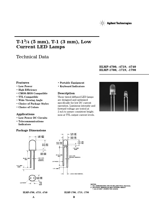
HLMP-7000, -7019, -7040Package DimensionsA BHLMP-1700, -1719, -1790HLMP-4700, -4719, -4740Note:1. θ1/2 is the typical off-axis angle at which the luminous intensity is half the axial luminous intensity.Part Numbering SystemHLMP-X7XX - X X X XXMechanical Option00: Bulk01: Tape & Reel, Crimped Leads02, BH: Tape & Reel, Straight LeadsA1, B1: Right Angle Housing, Uneven LeadsA2, B2: Right Angle Housing, Even LeadsFH: 2 Iv bins select with Inventory ControlColor Bin Options0: Full color bin distributionB: Color bins 2 & 3 onlyMaximum Iv Bin Options0: Open (No. max. limit)Others: Please refer to the Iv bin TableMinimum Iv Bin OptionsPlease refer to the Iv Bin TableColor Option00: GaP HER19: GaP Yellow40: GaP Green90: GaP GreenPackage Options4: T-13/4 (5 mm)1: T-1 (3 mm)Electrical/Optical Characteristics at T A = 25°CTest Symbol Description T-13/4T-1Min.Typ.Max.Units Conditions V F Forward Voltage47001700 1.7 2.0V 2 mA47191719 1.8 2.547401790 1.9 2.2V R Reverse Breakdown47001700 5.0V I R = 50 µA Voltage47191719 5.047401790 5.0λd Dominant47001700626nm Note 1 Wavelength4719171958547401790569∆λ1/2Spectral Line4700170040nmHalfwidth47191719364740179028τS Speed of Response4700170090ns471917199047401790500C Capacitance4700170011pF V F = 0,4719171915 f = 1 MHz4740179018RθJ-PIN Thermal47001700260[3]°C/W Junction to Resistance47191719290[4]Cathode Lead47401790λPEAK Peak Wavelength47001700635nm Measurement47191719583at peak47401790565ηV Luminous Efficacy47001700145lumens Note 247191719500watt47401790595Notes:1. The dominant wavelength, λd, is derived from the CIE chromaticity diagram and represents the single wavelength which defines thecolor of the device.2. The radiant intensity, I e, in watts per steradian, may be found from the equation I e = I V/ηV, where I V is the luminous intensity incandelas and ηV is luminous efficacy in lumens/watt.3. T-13/4.4. T-1.ParameterMaximum RatingUnits Power DissipationRed 24mW(Derate linearly from 92°C at 1.0 mA/°C)Yellow 36Green24DC and Peak Forward Current7mA Transient Forward Current (10 µs Pulse)[1]500mA Reverse Voltage (I R= 50 µA) 5.0VOperating Temperature Range Red/Yellow -55°C to 100°C Green-20°C to 100°CStorage Temperature Range -55°C to +100°C Lead Soldering Temperature 260°C for 5 seconds[1.6 mm (0.063 in.) from body]Note:1. The transient peak current is the maximum non-recurring peak current the devices can withstand without damaging the LED die and wire bonds. It is not recommended that the device be operated at peak currents beyond the Absolute Maximum Peak Forward Current.Figure 2. Forward Current vs. Forward Voltage.Figure 3. Relative Luminous Intensity vs. Forward Current.VOLTAGE – V624810Maximum tolerance for each bin limit is ±18%.Maximum tolerance for each bin limit is ±18%.Maximum tolerance for each bin limit is ±18%.Tolerance for each bin limit is ±0.5 nm.Mechanical Option MatrixMechanical Option Code Definition00Bulk Packaging, minimum increment 500 pcs/bag01Tape & Reel, crimped leads, min. increment 1300 pcs/bag for T-1 3/4, 1800pcs/bag for T-102Tape & Reel, straight leads, min. increment 1300 pcs/bag for T-1 3/4, 1800pcs/bag for T-1A1T-1, Right Angle Housing, uneven leads, minimum increment 500 pcs/bagA2T-1, Right Angle Housing, even leads, minimum increment 500 pcs/bagB1T-1 3/4, Right Angle Housing, uneven leads, minimum increment 500 pcs/bagB2T-1 3/4, Right Angle Housing, even leads, minimum increment 500 pcs/bagBH T-1, Tape & Reel, straight leads, minimum increment 2000 pcs/bagFH Devices that require inventory control and 2 I v bin selectR1Tape & Reel, crimped leads, reeled counter clockwise, cathode lead leavingthe reel firstNote:All categories are established for classification of products. Products may not be available in all categories. Please contact your local Agilent representative for further clarification/information./semiconductors For product information and a complete list of distributors, please go to our web site.For technical assistance call:Americas/Canada: +1 (800) 235-0312 or (916) 788-6763Europe: +49 (0) 6441 92460China: 10800 650 0017Hong Kong: (+65) 6756 2394India, Australia, New Zealand: (+65) 6755 1939 Japan: (+81 3) 3335-8152(Domestic/Interna-tional), or 0120-61-1280(Domestic Only) Korea: (+65) 6755 1989Singapore, Malaysia, Vietnam, Thailand, Philippines, Indonesia: (+65) 6755 2044 Taiwan: (+65) 6755 1843Data subject to change.Copyright © 2003 Agilent Technologies, Inc. September 10, 20035988-8054EN。
和利时电机产品说明书
版权申明北京和利时电机技术有限公司保留所有权力。
说明书的内容参照了相关法律基准和行业基准。
使用产品时,如对本说明书提供的内容有疑问,请向购买产品的销售人员咨询,或致电客户服务热线,或致信本公司邮箱。
由于产品的不断更新升级,和利时电机保留在不事先通知的情况下,修改本手册中的产品和产品规格参数等文件的权利,提示客户请使用最新版本的说明书。
和利时电机具有本产品及其软件的专利权、版权和其它知识产权。
未经许可,不得直接或者间接地复制、制造、加工、使用本产品及其相关部分。
和利时电机具有本说明书的著作权,未经许可,不得修改、复制说明书的全部或部分内容。
版本号 03/2016‐ 1 ‐目录第一章参数 ....................................................................................................... - 3 -1.1. 平台选择............................................................................................................................ - 3 -1.2. 游戏参数............................................................................................................................ - 3 -1.3. 六轴的位置信息................................................................................................................ - 4 -1.4. 体感参数............................................................................................................................ - 4 -1.5. 平台的机械参数................................................................................................................ - 5 -1.6. UDP端口号和采样时间 .................................................................................................. - 7 - 第二章函数 ....................................................................................................... - 8 -2.1. 函数的返回值.................................................................................................................... - 8 -2.2. 平台类型选择函数............................................................................................................ - 8 -2.3. 体感参数复位函数............................................................................................................ - 8 -2.4. 参数传递函数.................................................................................................................... - 8 -2.5. 机械参数初始化函数........................................................................................................ - 8 -2.6. 打开UDP端口函数 ......................................................................................................... - 8 -2.7. 体感+反解算法函数 ......................................................................................................... - 9 -2.8. 平台复位函数函数............................................................................................................ - 9 -2.9. 平台到达中位高度函数.................................................................................................... - 9 -2.10. 平台到达零位函数............................................................................................................ - 9 -2.11. 关闭UDP端口函数 ......................................................................................................... - 9 -2.12. 函数调用顺序.................................................................................................................... - 9 -‐ 2 ‐‐ 3 ‐第一章 参数1.1.平台选择SIM_CUE_DLL.dll 动态链接库集合了六自由度、三加一旋转轴四自由度、三自由度三种平台的体感算法以及直接进行电动缸位置控制。
HLMP-BL01-S0TYY中文资料
Agilent HLMP-ABxx, HLMP-BBxx, HLMP-ADxx, HLMP-BDxx, HLMP-AGxx, HLMP-BGxx, HLMP-ALxx, HLMP-BLxx,HLMP-AMxx, HLMP-BMxx T-13/4 (5 mm)Oval Precision Optical Performance AlInGaP and InGaN Lamps Data SheetFeatures•Well defined spatial radiation pattern•Viewing angles:Major axis 70°Minor axis 35°•High luminous output•Red and Amber Intensity are available for:AlInGaP (Bright)AlInGaP II (Brightest)•Colors:472 nm blue 526 nm green 626 nm red 630 nm red 590 nm amber 592 nm amber•Superior resistance to moisture •UV resistant epoxyBenefits•Viewing angle designed for wide field of view application•Red, green, and blue radiation patterns matched for full color sign•Superior performance in outdoor environments Applications•Full color/video signsDescriptionThese Precision O ptical Performance Oval LEDs are specifically designed for full color/video and passenger information signs. The oval shaped radiation pattern(35°x 70°) and high luminous intensity ensure that these devices are excellent for wide field of view outdoor application where a wide viewing angle and readability in sunlight areessential. These lamps have very smooth, matched radiation patterns ensuring consistent color mixing in full colorapplications, message uniformity across the viewing angle of the sign.High efficiency LED material is used in these lamps: Aluminum Indium Gallium Phosphide (AlInGaP) for amber and red,and Indium Gallium Nitride(InGaN) for blue and green. Each lamp is made with an advance optical grade epoxy offering superior high temperature and high moisture resistance in outdoor applications. The package epoxy contains both UV-A and UV-B inhibitors to reduce the effects of long term exposure to direct sunlight.Designers can select parallel or perpendicular orientation. Both lamps are available in tinted version.CAUTION: The blue and green LEDs are Class 1 ESD sensitive. Please observe appropriate precautions during handling and processing. Refer to Agilent Application Note AN-1142 for additio nal details.Table 1. Device Selection Guide for AlInGaP IIColor and Luminous Luminous ForwardDominant Intensity,Intensity,Voltage,LeadsWavelength I v (mcd) at I v (mcd) at V f (V)with Leadframe Package Part Numberλd (nm) Typ.20 mA Min.20 mA Max.Max.Stand-offs Orientation Drawing HLMP-AD06-P00xx Red 630880 2.4No Parallel A HLMP-AD06-P0Txx Red 630880 2.6No Parallel A HLMP-AD16-P00xx Red 630880 2.4Yes Parallel B HLMP-AD16-P0Txx Red 630880 2.6Yes Parallel B HLMP-AD16-RS0xx Red 63015002500 2.6Yes Parallel B HLMP-AD16-RSTxx Red 63015002500 2.6Yes Parallel B HLMP-AD16-RU0xx Red 63015004200 2.4Yes Parallel B HLMP-AD16-RUTxx Red 63015004200 2.6Yes Parallel B HLMP-AD16-ST0xx Red 63019003200 2.4Yes Parallel B HLMP-AD16-STTxx Red 63019003200 2.6Yes Parallel B HLMP-AL06-L00xx Amber 592400 2.4No Parallel A HLMP-AL06-L0Rxx Amber 592400 2.6No Parallel A HLMP-AL06-N00xx Amber 592680 2.4No Parallel A HLMP-AL06-N0Rxx Amber 592680 2.6No Parallel A HLMP-AL16-N00xx Amber 592680 2.4Yes Parallel B HLMP-AL16-N0Rxx Amber 592680 2.6Yes Parallel B HLMP-AL16-PSRxx Amber 5928802500 2.6Yes Parallel B HLMP-AL16-QR0xx Amber 59211501900 2.4Yes Parallel B HLMP-AL16-QRRxx Amber 59211501900 2.6Yes Parallel B HLMP-BD06-P00xx Red 630880 2.4No Perpendicular C HLMP-BD06-P0Txx Red 630880 2.6No Perpendicular C HLMP-BD06-RS0xx Red 63015002500 2.4No Perpendicular C HLMP-BD06-RSTxx Red 63015002500 2.6No Perpendicular C HLMP-BD16-P00xx Red 630880 2.4Yes Perpendicular D HLMP-BD16-P0Txx Red 630880 2.6Yes Perpendicular D HLMP-BD16-RU0xx Red 63015004200 2.4Yes Perpendicular D HLMP-BD16-RUTxx Red 63015004200 2.6Yes Perpendicular D HLMP-BD16-ST0xx Red 63019003200 2.4Yes Perpendicular D HLMP-BD16-STTxx Red 63019003200 2.6Yes Perpendicular D HLMP-BL06-N00xx Amber 592680 2.4No Perpendicular C HLMP-BL06-N0Rxx Amber 592680 2.6No Perpendicular C HLMP-BL06-QRKxx Amber 59211501900 2.4No Perpendicular C HLMP-BL06-QRSxx Amber 59211501900 2.6No Perpendicular C HLMP-BL16-N00xx Amber 592680 2.4Yes Perpendicular D HLMP-BL16-N0Rxx Amber 592680 2.6Yes Perpendicular D HLMP-BL16-PS0xx Amber 5928802500 2.4Yes Perpendicular D HLMP-BL16-PSRxx Amber 5928802500 2.6Yes Perpendicular DTable 2. LED IndicatorsDevice Selection Guide for AlInGaPColor and Luminous LuminousDominant Intensity,Intensity,LeadsWavelength I v (mcd) at I v (mcd) at with Leadframe Package Part Numberλd (nm) Typ.20 mA Min.20 mA Max.Stand-offs Orientation Drawing HLMP-AG01-K00xx Red 626310No Parallel A HLMP-AG11-KN0xx Red 626310880Yes Parallel B HLMP-AL01-K00xx Amber 590310No Parallel A HLMP-AL01-LP0xx Amber 5904001150No Parallel A HLMP-AL01-NR0xx Amber 5906801900No Parallel A HLMP-AL11-KN0xx Amber 590310880Yes Parallel B HLMP-AL11-NR0xx Amber 5906801900Yes Parallel B HLMP-BG01-LM0xx Red 626400520No Perpendicular C HLMP-BG01-MN0xx Red 626520880No Perpendicular C HLMP-BG11-KN0xx Red 626310880Yes Perpendicular D HLMP-BL01-NR0xx Amber 5906801900No Perpendicular C HLMP-BL11-KN0xx Amber 590310880Yes Perpendicular D HLMP-BL11-NR0xx Amber 5906801900Yes Perpendicular DTable 3. Device Selection Guide for InGaNColor and Dominant Luminous Intensity,Leads with Leadframe Package Part Number Wavelength λd (nm) Typ. Iv (mcd) at 20 mA Min.Stand-offs Orientation Drawing HLMP-AB01-J00xx Blue 472240No Parallel A HLMP-BB11-J00xx Blue 472240Yes Perpendicular D HLMP-BB11-K00xx Blue 472310Yes Perpendicular D HLMP-BM11-L00xx Green 526400Yes Perpendicular D HLMP-BM11-Q00xx Green 5261150Yes Perpendicular D HLMP-AB11-J00xx Blue 472240Yes Parallel B HLMP-AM01-Q00xx Green 5261150No Parallel A HLMP-BB01-J0Bxx Blue 472240No Perpendicular C HLMP-BB11-KN0xx Blue 472310Yes Perpendicular D HLMP-BM01-L00xx Green 526400No Perpendicular C Tolerance for intensity range limit is ±15%.Part Numbering SystemHLMP-X X X X - X X X XXMechanical Options00: Bulk PackagingDD: Ammo PackYY: Flexi-Bin; Bulk PackagingZZ: Flexi-Bin; Ammo PackColor Bin0: No Color Bin LimitationR: Color Bins 1, 2, 4, and 6 with V F max of 2.6 VT: Red Color with V F max of 2.6 VB: Color bin 2 and 3 onlyK: Color bins 2 and 4 onlyS: Color bins 2 and 4 with VF max of 2.6 VMaximum Intensity Bin0: No Iv Bin LimitationMinimum Intensity BinTint Option1 or 6: Matching Color TintsStandoff Option0: Without1: WithColorB: 472 nm BlueD: 630 nm RedG: 626 nm RedL: 590 or 592 nm AmberM: 526 nm GreenPackageA: 5 mm 35° x 70° Oval, ParallelB: 5 mm 35° x 70° O val, PerpendicularPackage Dimensions5.00 ±(0.197 ±8.71 ± 0.200.50 ± 0.10SQ. TYP.5.00 ±(0.197 ±5.00 ±(0.197 ±5.00 ±(0.197 ±ABCDNOTES:1. ALL DIMENSIONS ARE IN MILLIMETERS (INCHES).2. LEADS ARE MILD STEEL, SOLDER DIPPED.3. TAPERS SHOWN AT TOP OF LEADS (BOTTOM OF LAMP PACKAGE) INDICATE AN EPOXY MENISCUS THAT MAY EXTEND ABOUT 1 mm (0.040 IN.) DOWN THE LEADS.4. RECOMMENDED PC BOARD HOLE DIAMETERS:– LAMP PACKAGES A AND C WITHOUT STAND-OFFS: FLUSH MOUNTING AT BASE OF LAMP PACKAGE = 1.143/1.067 mm (0.044/0.042 IN.).– LAMP PACKAGES B AND D WITH STAND-OFFS: MOUNTING AT LEAD STAND-OFFS.Absolute Maximum Ratings at T A = 25˚CParameter Blue and Green Red and Amber DC Forward Current[1]30 mA50 mAPeak Pulsed Forward Current[2]100 mA100 mAAverage Forward Current30 mA30 mAReverse Voltage (I R = 100 µA) 5 VReverse Voltage (I R = 10 µA) 5 VPower Dissipation120 mW120 mWLED Junction Temperature130°C130°COperating Temperature Range–40°C to +80°C–40°C to +100°C Storage Temperature Range–40°C to +100°C–40°C to +120°C Wave Soldering Temperature[3]250°C for 3 seconds250°C for 3 seconds Notes:1.Derate linearly from Figure 7.2.Duty Factor 30% KHz.3.1.59 mm (0.060 in.) below body.Electrical/Optical Characteristics at T A = 25°CParameter Symbol Min.Typ.Max.Units Test Conditions Typical Viewing AngleMajor2θ1/270degMinor35Forward Voltage V F V I F = 20 mARed (λd = 626 nm) 2.0 2.4Red (λd = 630 nm)Option xx0xx 2.2 2.4Option xxTxx 2.3 2.6Amber (λd = 590 nm) 2.0 2.4Amber (λd = 592 nm)Option xx0xx 2.2 2.4Option xxRxx, xxSxx 2.3 2.6Blue (λd = 472 nm) 3.5 4.0Green (λd = 526 nm) 3.5 4.0Reverse VoltageAmber, Red V R520V I R = 100 µABlue, Green5–I R = 10 µAPeak Wavelength Peak of Wavelength of Amber (λd = 592 nm)λpeak594nm Spectral Distribution Red (λd = 630 nm)639at I F = 20 mABlue (λd = 472 nm)470Green (λd = 526 nm)524Spectral Halfwidth Wavelength Width Amber (λd = 592 nm)∆λ1/217nm at Spectral Distribution Red (λd = 630 nm)171/2 Power Point at Blue (λd = 472 nm)35I F = 20 mAGreen (λd = 526 nm)47Capacitance V F = 0, F = 1 MHz Amber, Red C40pFBlue, Green43Luminous Efficacy Emitted Luminous Amber (λd = 592 nm)ηv500lm/W Power/Emitted Radiant Red (λd = 630 nm)155Power at I F = 20 mA Blue (λd = 472 nm)75Green (λd = 526 nm)520Thermal Resistance RΘJ-PIN240°C/W LED Junction-to-Cathode LeadNotes:1.2θ1/2 is the off-axis angle where the luminous intensity is 1/2 the on-axis intensity.2.The radiant intensity, I e in watts per steradian, may be found from the equation I e = I v/ηv where I v is the luminous intensity in candelas and ηv isthe luminous efficacy in lumens/watt.3.The luminous intensity is measured on the mechanical axis of the lamp package.4.The optical axis is closely aligned with the package mechanical axis.5.The dominant wavelength, λd, is derived from theCIE Chromaticity Diagram and represents the color of the lamp.6.For Options -xxRxx, -xxSxx and -xxTxx, max. forward voltage (Vf) is 2.6 V. Refer to Vf bin table.Figure 1. Relative intensity vs. wavelength.Figure 2. Blue, green forward current vs.forward voltage.WAVELENGTH – nmR E L A T I V E I N T E N S I T Y1.00.500.40.30.20.10.60.70.80.9030251510I F – F O R W A R D C U R R E N T – m AV F – FORWARD VOLTAGE – V2.42.83.2 3.6520 2.6 3.0 3.4Figure 3a. Amber, red forward current vs.forward voltage.Figure 4. Blue, green relative luminous intensity vs. forward current.1.50.5I N T E N S I T Y N O R M A L I Z E D A T 20 m AI F – FORWARD CURRENT – mA01020301.051525C U R R E N T – m AV F – FORWARD VOLTAGE – V Figure 3b. Forward current vs. forward voltage for option -xxTxx red, and option -xxRxx and -xxSxx amber.D C F O R W A R D C U R RE N T – m AFORWARD VOLTAGE – VFigure 6. Blue, green maximum forward current vs. ambient temperature.Figure 7. Amber, red maximum forward current vs. ambient temperature.I F – F O R W A R D C U R R E N T – m A0T A – AMBIENT TEMPERATURE – °C40804020102060301005152535I F – F O R W A R D CU R R E N T – m AT A – AMBIENT TEMPERATURE – °CFigure 5. Amber, red relative luminous intensity vs. forward current.R E L A T I V E I N T E N S I T Y (N OR M A L I Z E D A T 20 m A )FORWARD CURRENT – mAFigure 8. Spatial radiation pattern – 35 x 70 degree lamps.R E L A T I V E I N T E N S I T Y – %1000VERTICAL ANGULAR DISPLACEMENT – DEGREES8060507020501030404020-10-30-50903010-20-40R E L A T I V E I N T E N S I T Y – %1000HORIZONTAL ANGULAR DISPLACEMENT – DEGREES8060507020501030404020-10-30-50903010-20-40Intensity Bin Limits (mcd at 20 mA)Bin Name Min.Max.G 140180H 180240J 240310K 310400L 400520M 520680N 680880P 8801150Q 11501500R 15001900S 19002500T 25003200U19002500Tolerance for each bin limit is ±15%.Amber Color Bin Limits (nm at 20 mA)Bin Name Min.Max.1584.5587.02587.0589.54589.5592.06592.0594.5Tolerance for each bin limit is ± 0.5 nm.Notes:1.All bin categories are established for classifi-cation of products. Products may not beavailable in all bin categories. Please contact your Agilent representative for further information.2. Vf bin table only available for those numbers with options -xxRxx, -xxSxx, -xxTxx.Blue Color Bin Limits (nm at 20 mA)Bin Name Min.Max.1460.0464.02464.0468.03468.0472.04472.0476.05476.0480.0Tolerance for each bin limit is ± 0.5 nm.Green Color Bin Limits (nm at 20 mA)Bin Name Min.Max.1520.0524.02524.0528.03528.0532.04532.0536.05536.0540.0Tolerance for each bin limit is ±0.5 nm.Vf Bin Table [2]Bin Id Min.Max.VA 2.0 2.2VB 2.2 2.4VC2.4 2.6/semiconductors For product information and a complete list of distributors, please go to our web site.For technical assistance call:Americas/Canada: +1 (800) 235-0312 or (916) 788-6763Europe: +49 (0) 6441 92460China: 10800 650 0017Hong Kong: (+65) 6756 2394India, Australia, New Zealand: (+65) 6755 1939 Japan: (+81 3) 3335-8152(Domestic/Interna-tional), or 0120-61-1280(Domestic Only) Korea: (+65) 6755 1989Singapore, Malaysia, Vietnam, Thailand, Philippines, Indonesia: (+65) 6755 2044 Taiwan: (+65) 6755 1843Data subject to change.Copyright © 2004 Agilent Technologies, Inc. August 27, 20045988-9224EN。
HL-1说明书
HL-1 开发板使用说明书 慧净电子-做人人都买得起的 51 单片机开发板
为低电平,那么以后当输入端无论再怎么变化,输出端都不会变化而是保持刚才 第 11 脚在下降沿(由高电平到低电平跳变)之间时输入端的值,这样就达到了 锁存数据的目的,这也就是所谓的总线设计思路,一个 8 位的数据线加一个锁存 器后就可以扩接多个元件,当选通哪个元件的片选信号,就送数据给那个元件。 先说这个元件,以后用到别的元件我们再解释。下面开始讲解例程。
HL-1 开发板使用说明书 慧净电子-做人人都买得起的 51 单片机开发板
学讲座走 10 天,之后必将会有非常大的收获。共享配套视频光盘,一般在网上 下载:跟着教程学习,开始讲了流水灯设计流程,实验板上其余的功能就需要靠 用户自来对它进行编程并实现它们了,这样学起来只是时间会稍长些,感觉会累 点,但只要大家肯努力,终究也一定会学会的。
慧净单片机学习网: 慧净淘宝网:/
HL-1 开发板使用说明书 慧净电子-做人人都买得起的 51 单片机开发板
[源代码] #include<reg51.h> /**********************************************************
HL-1 开发板使用说明书 慧净电子-做人人都买得起的 51 单片机开发板
HL-1 单片机实验板使用手册
目录 HL-1 单片机实验板使用手册.................................................................................. 目录............................................................................................................................. 1.准备工作................................................................................................................. 2 学习方法介绍.......................................................................................................... 3.实验例程详细解答.................................................................................................. 3.1 闪烁灯............................................................................................................. 3.2 流水灯............................................................................................................. 3.3 单键识别......................................................................................................... 3.4 59 秒计数器.................................................................................................. 3.5 矩阵键盘检测...............................................................................................
iw1710规格书中文版

IW1710机翻中文版IW1710数字PWM电流模式控制器,应用准谐工作模式1.0 产品特点原边反应简化了设计,并去除了光耦准谐振模式,提高的整体效率EZ-EMI ®设计,轻松满足全球EMI标准高达130 kHz的开关频率,适用于小尺寸变压器极为严格的输出电压调节无需外部补偿元件符合CEC/ EPA空载功耗和平均效率规定置输出恒流控制与初级侧反应低启动电流〔典型值10μA〕置软启动置短路保护和输出过压保护可选的AC线路欠压/过电压保护轻负载时工作在PFM模式电流检测电阻短路保护过温保护2.0 说明iW1710是一款高性能的AC/DC电源控制器,它采用数字控制技术,打造峰值电流PWM模式反激式电源。
iW1700工作在准谐振模式,在重负载提供高效率,以及一些关键的置保护功能,同时最大限度地减少了外部元件数量,简化了EMI设计,降低材料本钱的总费用。
iW1710不再需要次级反应电路,同时实现出色的线性和负载调节。
它在去除了环路补偿元件的同时保证稳定的工作。
脉冲波形分析使环路响应是比传统的解决方案快得多,从而提高了动态负载响应。
置电流限制功能可优化变压器设计,通用的离线应用程序在很宽的输入电压围。
在轻负载时超低的工作电流和和待机功率,保证iW1710是新管理标准和平均效率应用的理想选择。
3.0 应用3.1 典型应用电路4.0 引脚说明引脚名称类型说明1 NC - 悬空脚2 V SENSE模拟输入辅助电压检测〔用于初级端调节〕3 V IN模拟输入输入端电压平均值检测4 SD 模拟输入外部关断控制。
通过一个电阻连接到地,如不使用见10.165 GND 地地6 I SENSE模拟输入初级电流检测〔用于逐周期峰值电流控制和限制〕7 OUTPUT 输出外部MOSFET管栅极驱动。
8 V CC电源输入控制逻辑的电源和电压检测的上电复位电路。
5.0 额定最大值6.0 电气特性VCC=12V -40℃至85℃7.0 典型性能特性8.0 功能框图9.0 工作原理iW1710采用了专有的初级侧控制技术,去除了光耦反应和传统设计所需的二次调节电路的数字控制器。
- 1、下载文档前请自行甄别文档内容的完整性,平台不提供额外的编辑、内容补充、找答案等附加服务。
- 2、"仅部分预览"的文档,不可在线预览部分如存在完整性等问题,可反馈申请退款(可完整预览的文档不适用该条件!)。
- 3、如文档侵犯您的权益,请联系客服反馈,我们会尽快为您处理(人工客服工作时间:9:00-18:30)。
HLMP-7000, -7019, -7040Package DimensionsA BHLMP-1700, -1719, -1790HLMP-4700, -4719, -4740Note:1. θ1/2 is the typical off-axis angle at which the luminous intensity is half the axial luminous intensity.Part Numbering SystemHLMP-X7XX - X X X XXMechanical Option00: Bulk01: Tape & Reel, Crimped Leads02, BH: Tape & Reel, Straight LeadsA1, B1: Right Angle Housing, Uneven LeadsA2, B2: Right Angle Housing, Even LeadsFH: 2 Iv bins select with Inventory ControlColor Bin Options0: Full color bin distributionB: Color bins 2 & 3 onlyMaximum Iv Bin Options0: Open (No. max. limit)Others: Please refer to the Iv bin TableMinimum Iv Bin OptionsPlease refer to the Iv Bin TableColor Option00: GaP HER19: GaP Yellow40: GaP Green90: GaP GreenPackage Options4: T-13/4 (5 mm)1: T-1 (3 mm)Electrical/Optical Characteristics at T A = 25°CTest Symbol Description T-13/4T-1Min.Typ.Max.Units Conditions V F Forward Voltage47001700 1.7 2.0V 2 mA47191719 1.8 2.547401790 1.9 2.2V R Reverse Breakdown47001700 5.0V I R = 50 µA Voltage47191719 5.047401790 5.0λd Dominant47001700626nm Note 1 Wavelength4719171958547401790569∆λ1/2Spectral Line4700170040nmHalfwidth47191719364740179028τS Speed of Response4700170090ns471917199047401790500C Capacitance4700170011pF V F = 0,4719171915 f = 1 MHz4740179018RθJ-PIN Thermal47001700260[3]°C/W Junction to Resistance47191719290[4]Cathode Lead47401790λPEAK Peak Wavelength47001700635nm Measurement47191719583at peak47401790565ηV Luminous Efficacy47001700145lumens Note 247191719500watt47401790595Notes:1. The dominant wavelength, λd, is derived from the CIE chromaticity diagram and represents the single wavelength which defines thecolor of the device.2. The radiant intensity, I e, in watts per steradian, may be found from the equation I e = I V/ηV, where I V is the luminous intensity incandelas and ηV is luminous efficacy in lumens/watt.3. T-13/4.4. T-1.ParameterMaximum RatingUnits Power DissipationRed 24mW(Derate linearly from 92°C at 1.0 mA/°C)Yellow 36Green24DC and Peak Forward Current7mA Transient Forward Current (10 µs Pulse)[1]500mA Reverse Voltage (I R= 50 µA) 5.0VOperating Temperature Range Red/Yellow -55°C to 100°C Green-20°C to 100°CStorage Temperature Range -55°C to +100°C Lead Soldering Temperature 260°C for 5 seconds[1.6 mm (0.063 in.) from body]Note:1. The transient peak current is the maximum non-recurring peak current the devices can withstand without damaging the LED die and wire bonds. It is not recommended that the device be operated at peak currents beyond the Absolute Maximum Peak Forward Current.Figure 2. Forward Current vs. Forward Voltage.Figure 3. Relative Luminous Intensity vs. Forward Current.VOLTAGE – V624810Maximum tolerance for each bin limit is ±18%.Maximum tolerance for each bin limit is ±18%.Maximum tolerance for each bin limit is ±18%.Tolerance for each bin limit is ±0.5 nm.Mechanical Option MatrixMechanical Option Code Definition00Bulk Packaging, minimum increment 500 pcs/bag01Tape & Reel, crimped leads, min. increment 1300 pcs/bag for T-1 3/4, 1800pcs/bag for T-102Tape & Reel, straight leads, min. increment 1300 pcs/bag for T-1 3/4, 1800pcs/bag for T-1A1T-1, Right Angle Housing, uneven leads, minimum increment 500 pcs/bagA2T-1, Right Angle Housing, even leads, minimum increment 500 pcs/bagB1T-1 3/4, Right Angle Housing, uneven leads, minimum increment 500 pcs/bagB2T-1 3/4, Right Angle Housing, even leads, minimum increment 500 pcs/bagBH T-1, Tape & Reel, straight leads, minimum increment 2000 pcs/bagFH Devices that require inventory control and 2 I v bin selectR1Tape & Reel, crimped leads, reeled counter clockwise, cathode lead leavingthe reel firstNote:All categories are established for classification of products. Products may not be available in all categories. Please contact your local Agilent representative for further clarification/information./semiconductors For product information and a complete list of distributors, please go to our web site.For technical assistance call:Americas/Canada: +1 (800) 235-0312 or (916) 788-6763Europe: +49 (0) 6441 92460China: 10800 650 0017Hong Kong: (+65) 6756 2394India, Australia, New Zealand: (+65) 6755 1939 Japan: (+81 3) 3335-8152(Domestic/Interna-tional), or 0120-61-1280(Domestic Only) Korea: (+65) 6755 1989Singapore, Malaysia, Vietnam, Thailand, Philippines, Indonesia: (+65) 6755 2044 Taiwan: (+65) 6755 1843Data subject to change.Copyright © 2003 Agilent Technologies, Inc. September 10, 20035988-8054EN。