LF27中文资料
数控机床用直线光栅尺(中文)

LC LF
LC 400 LC 100 LF 481 LF 183 LS 487 LS 187
LS
LS 477 LS 177
17
HCN 2008
8:1Vpp 9:带串口的绝对式光栅尺
机床用直线光栅尺
HCN 2008
应用
要求
高精度 热特性 稳定性
HEIDENHAIN Product
高性能机床,
磨床,车床,铣床
LF LC LS 1xx, LS 4xx LB LS 1679
热特性 测量步距,价格
大型机床 折弯机等
经济性 坚固耐用 数显用光栅尺
~ 1 Vpp
大型机床
LS 388C LS 328C LS 378C LS 688C LS 628C LS 678C
20 µ m 增量式 玻璃刻线 ± 10 µm ± 10 µm ± 5 µm ~ 1 Vpp TTL
通用型机床 如手动机床、 EDM和刀具调 整等
LS 1679
100µm
增量式 玻璃刻线 内置导轨
HCN 2008
8
不合理的安装
HCN 2008
9
读数头安装块
HCN 2008
l
b h
10
Abbé误差的补偿
b
导轨
HCN 2008
b
丝杠
ΔP
S
重心
P
ΔP 2
光栅尺
Abbé误差的补偿
高速铣床 © Heller
tan P P2 / b 1 /b P b tan 1 P P P1 2 2
Distance d, mm 1.5 ±0.3 1.0 ±0.3
Distance a, mm 2.0 ± 0.3 0.0 ± 0.2
LF33中文资料

Symbol
Parameter
Vi DC Input Voltage
Io Output Current
Ptot Power Dissipation
Tstg Storage Temperature Range
Top Operating Junction Temperature Range
(*) For 18 < VIN < 40 the regulator is in shut-down
LF12CP LF12ABP LF15CP LF15ABP LF25CP LF25ABP LF27CP LF27ABP LF30CP LF30ABP LF33CP LF33ABP LF35CP LF35ABP LF40CP LF40ABP LF45CP LF45ABP LF47CP LF47ABP LF50CP LF50ABP LF52CP LF52ABP LF55CP LF55ABP LF60CP LF60ABP LF80CP LF80ABP LF85CP LF85ABP LF90CP LF90ABP LF120CP LF120ABP
ORDERING NUMBERS
Type
PENTAWAT T
TO-220
ISOWATT 220
DPAK
PPAK
LF12C (*)
LF12CV5V
LF12AB (*) LF15C (*) LF15AB (*) LF25C LF25AB LF27C LF27AB LF30C LF30AB
LF12ABV5V LF15CV5V LF15ABV5V LF25CV5V LF25ABV5V LF27CV5V LF27ABV5V LF30CV5V LF30ABV5V
元器件交易网
ASCII码中英文对照表

关键字:最全ASCII码对照表ASCII码值对照表 ASCI I码值A SCII码中英文对照表Bi n DecH ex 缩写/字符解释0000 0000 0 00 NUL(null) 空字符0000 0001 1 01 SOH (start of h andin g) 标题开始0000 0010202 S TX (s tartof te xt) 正文开始00000011 303 ET X (en d oftext)正文结束0000 0100 4 04 EOT(endof tr ansmi ssion) 传输结束0000 0101 5 05 ENQ (enq uiry)请求00000110 606 AC K (ac knowl edge)收到通知0000 0111 7 07 BEL (bel l) 响铃0000 1000 8 08 BS(back space) 退格0000 1001 9 09 HT(hori zonta l tab) 水平制表符0000 1010 10 0A LF (N L lin e fee d, ne w lin e) 换行键00001011 11 0B VT(vert icaltab)垂直制表符00001100 12 0C FF(NP f orm f eed,new p age)换页键0000 1101 13 0D C R (ca rriag e ret urn)回车键0000 111014 0E SO (shi ft ou t) 不用切换0000 111115 0F SI (shi ft in) 启用切换0001 0000 16 10 DLE(data link esca pe) 数据链路转义0001 0001 17 11 DC1(devi ce co ntrol 1) 设备控制10001 0010 18 12 DC2 (devic e con trol2) 设备控制20001 0011 19 13 D C3 (d evice cont rol 3) 设备控制30001 010020 14 DC4 (de vicecontr ol 4)设备控制4 00010101 21 15 NAK (neg ative ackn owled ge) 拒绝接收0001 0110 22 16 S YN (s ynchr onous idle) 同步空闲0001 0111 23 17 ETB(endof tr ans.block) 传输块结束0001 1000 24 18 C AN (c ancel) 取消0001 1001 25 19 EM (e nd of medi um) 介质中断0001 101026 1A SU B (su bstit ute)替补0001 101127 1B ES C (es cape)溢出0001 110028 1C FS (fil e sep arato r) 文件分割符0001 1101 29 1D GS (group sepa rator) 分组符0001 111030 1E RS (rec ord s epara tor)记录分离符00011111 31 1F US(unit sepa rator) 单元分隔符0010 0000 32 20 空格0010 0001 33 21 !0010 0010 34 22 "0010 0011 35 23 #0010 0100 36 24 $0010 0110 38 26 & 0010 0111 39 27 ' 0010 1000 40 28 ( 0010 1001 41 29 ) 0010 1010 42 2A * 0010 1011 43 2B + 0010 1100 44 2C , 0010 1101 45 2D -0010 1110 46 2E . 0010 1111 47 2F / 0011 0000 48 30 0 0011 0001 49 31 1 0011 0010 50 32 2 0011 0011 51 33 3 0011 0100 52 34 4 0011 0101 53 35 5 0011 0110 54 36 6 0011 0111 55 37 7 0011 1000 56 38 8 0011 1001 57 39 9 0011 1010 58 3A : 0011 1011 59 3B ; 0011 1100 60 3C < 0011 110161 3D =0011 111062 3E >0011 111163 3F ?0100 000064 40 @0100 000165 41 A0100 001066 42 B0100 001167 43 C0100 010068 44 D0100 010169 45 E0100 011070 46 F0100 011171 47 G0100 100072 48 H0100 100173 49 I0100 101074 4A J0100 101175 4B K0100 110076 4C L0100 110177 4D M0100 111078 4E N0100 111179 4F O0101 000080 50 P0101 000181 51 Q0101 001183 53 S0101 010084 54 T0101 010185 55 U0101 011086 56 V0101 011187 57 W0101 100088 58 X0101 100189 59 Y0101 101090 5A Z0101 101191 5B [0101 110092 5C \0101 110193 5D ]0101 111094 5E ^0101 111195 5F _0110 000096 60 `0110 000197 61 a0110 001098 62 b0110 001199 63 c0110 0100100 64 d 01100101 101 65 e 0110 0110 102 66 f 0110 0111 10367 g 0110 1000 104 68 h0110 1001105 69 i 01101010 106 6A j 0110 1011 107 6B k 0110 1100 1086C l 0110 1101 109 6D m0110 1110110 6E n 01101111 111 6F o 0111 0000 112 70 p 0111 0001 11371 q 0111 0010 114 72 r0111 0011115 73 s 01110100 116 74 t 0111 0101 117 75 u 0111 0110 11876 v 0111 0111 119 77 w0111 1000120 78 x 01111001 121 79 y 0111 1010 122 7A z 0111 1011 1237B { 0111 1100 124 7C |0111 1101125 7D } 01111110 126 7E ~01111111 127 7F DEL(dele te) 删除E SC键V K_ESC APE (27)回车键:VK_RE TURN(13)TAB键: VK_TAB(9)C aps L ock键: VK_C APITA L (20)Shi ft键: VK_SHIFT ()C trl键:V K_CON TROL(17)Alt键: VK_M ENU (18)空格键: VK_S PACE(/32)退格键: VK_BACK (8)左徽标键:VK_LW IN (91)右徽标键: VK_LWIN (92)鼠标右键快捷键:V K_APP S (93)In sert键: VK_INSE RT (45)Ho me键: VK_H OME (36)P age U p: VK_PRIO R (33)Pag eDown: VK_NEXT(34)End键:VK_EN D (35)Del ete键: VK_D ELETE (46)方向键(←): VK_L EFT (37)方向键(↑):VK_UP (38)方向键(→): VK_RIGHT (39)方向键(↓): VK_DOWN(40)F1键: VK_F1 (112)F2键: VK_F2 (113)F3键:VK_F3 (114)F4键:V K_F4(115)F5键: VK_F5 (116)F6键: VK_F6 (117)F7键: VK_F7 (118)F8键:VK_F8 (119)F9键:V K_F9(120)F10键: VK_F10 (121)F11键: VK_F11 (122)F12键:VK_F12 (123)Nu m Loc k键:V K_NUM LOCK(144)小键盘0:V K_NUM PAD0(96)小键盘1: VK_NUMP AD0 (97)小键盘2: VK_NUMPA D0 (98)小键盘3: VK_N UMPAD0 (99)小键盘4:VK_NU MPAD0 (100)小键盘5:VK_NU MPAD0 (101)小键盘6:VK_NU MPAD0 (102)小键盘7:VK_NU MPAD0 (103)小键盘8:VK_NU MPAD0 (104)小键盘9:VK_NU MPAD0 (105)小键盘.:VK_DE CIMAL (110)小键盘*:VK_MU LTIPL Y (106)小键盘+: VK_M ULTIP LY (107)小键盘-: VK_SUBTR ACT (109)小键盘/: VK_DIVI DE (111)P auseBreak键: VK_PAUS E (19)Scr oll L ock键: VK_S CROLL (145)关键字:最全AS CII码对照表 AS CII码值对照表A SCII码值 ASC II码中英文对照表作者:f lydoo飞度欢迎加QQ编程群:26438718飞度编程学社博客:htt p://f lydoo s.blo g.16网盘软件下载:htt p://f lydoo.ys168.com。
常用战机中英文对照
美军英文型号中文格式备注1 备注2F-15 Eagle F-15战斗机F-15后边可能跟字母什么F-15A/B指早期型F-15C/D指后期型F-15E指最新型可写成“F-15沉默鹰”F-15J为日本服役的F-15 F-15K为韩国服役的空军专用F-16 Flacon F-16战斗机F-16后边可能跟字母什么F-16A/B指早期型F-16C/D指后期型F-16多个国家均有购买具体型号看文内国家再定空军专用F/A-18 Hornet F/A-18战斗机F指战斗机主要是用来打空中的飞机之类的,A指攻击机,主要用来打地面的坦克之类的。
F-18后边可能跟字母什么F-18A/B 指早期型F-18C/D指后期型,后有E/A-18G电子战用海军用F-22 Raptor F-22战斗机F-22是美国最先进的现役战斗机,目前只有F-22一个型号空军专用F-35 Lighting2 F-35战斗机美国最新的五代战斗机,分为F-35A空军型F-35B海军型(可短距离起降)F-35C海军陆战队型EA-6B Prowler EA-6B舰载攻击机航母专用的舰载机,已经很少了海军专用A-10 Warthog A-10攻击机对地攻击机空军专用C-130 Hercules C-130运输机美军最常用的战术运输机直接写C-130即可,或加上C-130后的字母如:C-130H之类的,广泛出口各国,多数国家均有使用按国别C-17 Global Master C-17运输机美军最常用的战略运输机直接写C-17运输机或C-17“环球霸王”战略运输机C-5 Galaxy C-5运输机目前美军服役的最大的战略运输机,比C-17还大,可写做C-5“银河”战略运输机B-2 Sprite B-2隐形轰炸机美军最先进的隐形轰炸机直接写作B-2隐形轰炸机或B-2轰炸机即可空军专用B-52 Stratofortress B-52战略轰炸机美军最长命的战略轰炸机,从50年代用到现在,常见的有B-52H轰炸机AH-1 Cobra AH-1武装直升机A是指武装H是指直升机,1是指型号,看到美军AH就是武装直升机的意思,AH-1有很多改型,名字都不一样。
项目管理术语表中英文对照
实际成本2. ACWP已完工作实际成本3. BAC完工预算4. CCB变更控制委员会5. COQ质量成本6. CPAF成本加奖励费用合同7. CPFF成本加固定费用合同8. CPI成本绩效指数9. CPIF成本加激励费用合同10. CPM关键路径法11. CV成本偏差12. EAC完工估算13. EF最早完成日期14. EMV预期货币价值15. ES最早开始日期16. ETC完工尚需估算17. EV挣值18. EVM挣值管理19. FF完成到完成20. FFP固定总价合同21. FMEA失效模式与影响分析22. FP-EPA总价加经济价格调整合同总价加激励费用合同24. FS完成到开始25. IFB投标邀请书26. LF最晚完成日期27. LOE支持型活动28. LS最晚开始日期29. OBS组织分解结构30. PDM紧前关系绘图法31. PMBOK项目管理知识体系32. PV计划价值33. QFD质量功能展开34. RACIRACI:责任分配矩阵的一种常见类型,使用执行、负责、咨询和知情等词语来定义干系人在项目活动中的参与状态。
35. RAM责任分配矩阵36. RBS风险分解结构37. RFI信息邀请书38. RFP建议邀请书39. RFQ报价邀请书40. SF开始到完成41. SOW工作说明书42. SPI进度绩效指数43. SS开始到开始44. SV进度偏差45. SWOT优势、劣势、机会与威胁46. TM工料47. WBS工作分解结构48. SWOT AnalysisSWOT分析对一个组织、项目或备选方案的优势、劣势、机会和威胁的分析。
49. Performance Reporting报告绩效见“工作绩效报告”。
50. Reporting Systems报告系统用于从一个或多个信息管理系统中生成或合并报告,并向项目干系人发送报告的设施、过程和程序。
51. Request for Quotation (RFQ)报价邀请书采购文件的一种,用来向潜在卖方征求对通用或标准产品或服务的报价。
PIC16LF1508-ISS;PIC16F1508-ISS;PIC16LF1509-ISS;PIC16F1509-ISS;中文规格书,Datasheet资料
Trademarks The Microchip name and logo, the Microchip logo, dsPIC, KEELOQ, KEELOQ logo, MPLAB, PIC, PICmicro, PICSTART, PIC32 logo, rfPIC and UNI/O are registered trademarks of Microchip Technology Incorporated in the U.S.A. and other countries. FilterLab, Hampshire, HI-TECH C, Linear Active Thermistor, MXDEV, MXLAB, SEEVAL and The Embedded Control Solutions Company are registered trademarks of Microchip Technology Incorporated in the U.S.A. Analog-for-the-Digital Age, Application Maestro, chipKIT, chipKIT logo, CodeGuard, dsPICDEM, , dsPICworks, dsSPEAK, ECAN, ECONOMONITOR, FanSense, HI-TIDE, In-Circuit Serial Programming, ICSP, Mindi, MiWi, MPASM, MPLAB Certified logo, MPLIB, MPLINK, mTouch, Omniscient Code Generation, PICC, PICC-18, PICDEM, , PICkit, PICtail, REAL ICE, rfLAB, Select Mode, Total Endurance, TSHARC, UniWinDriver, WiperLock and ZENA are trademarks of Microchip Technology Incorporated in the U.S.A. and other countries. SQTP is a service mark of Microchip Technology Incorporated in the U.S.A. All other trademarks mentioned herein are property of their respective companies. © 2011, Microchip Technology Incorporated, Printed in the U.S.A., All Rights Reserved. Printed on recycled paper. ISBN: 978-1-61341-726-3
ASCII码中英文对照
0001 0010 18 12 DC2 (device control 2) 设备控制2
0001 0101 21 15 NAK (negative acknowledge) 拒绝接收
0001 0110 22 16 SYN (synchronous idle) 同步空闲
0100 1110 78 4E N
0100 1111 79 4F O
0101 0000 80 50 P
0101 0001 81 51 Q
0000 1011 11 0B VT (vertical tab) 垂直制表符
0000 1100 12 0C FF (NP form feed, new page) 换页键
0010 0010 34 22 "
0010 0011 35 23 #
0010 0100 36 24 $
0010 0101 37 25 %
0000 0011 3 03 ETX (end of text) 正文结束
0000 0100 4 04 EOT (end of transmission) 传输结束
0100 0110 70 46 F
0100 0111 71 47 G
0100 1000 72 48 H
0100 1001 73 49 I
关键字:
Bin Dec Hex 缩写/字符 解释
0000 0000 0 00 NUL (null) 空字符
0000 1111 15 0F SI (shift in) 启用切换
0001 0000 16 10 DLE (data link escape) 数据链路转义
中英文翻译对照表
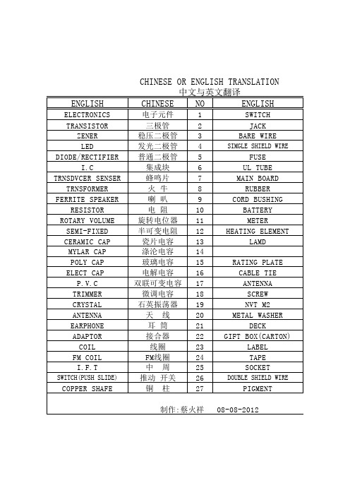
制作:蔡火祥 08-08-2012制作:蔡火祥 08-08-2012制作:蔡火祥 08-08-2012中文与英文翻译制作:蔡火祥 08-08-2012制作:蔡火祥 08-08-2012制作:蔡火祥 08-08-2012ESE OR ENGLISH TRANSLATION 中文与英文翻译制作:蔡火祥 08-08-2012制作:蔡火祥 08-08-2012常用词汇中英文对照序号英文中文序号英文中文序号英文中文1DENON天龙40POWER BUTTON开关键2MARANTZ马兰士41CARD CABLE软排线3PIONEER先锋42CUSHION SNOW保丽龙4NEW MODEL新机型43WASHER垫片5FRONT PANEL外面的面壳44GREASE润滑油6INNER PANEL里面的面壳45FELT绒布7MAIN CHASSIS底壳 底板46BRACKET支架8CD MECHA机芯47HEAT SINK散热器9BACK CHASSIS后板 后盖48WIRE线材10TOP COVER上盖 顶盖49BUSHING后板用的塞子11AC CORD电源线50PLATE接地片12LABEL贴纸51MAC ADDRESS MAC地址13PACKING包装52CODE物料编码14DISPLAY WINDOW镜片53SILVER银色15SCREW螺丝54BLACK黑色16BADGE铭牌55BONDING打胶处理17DOOR卡门56LUG WIRE地线18CABLE TIE扎带57RUNNINGCHANGE原来的使用完之后自动变更为新的 但不能乱用19CLAMP MTG锁螺丝的扎带20NUT螺母58SPERKER音箱21KNOB旋钮59SUB WOOFER低音炮22FOOT机脚60DOUBLE TAPE双面胶23FOOT CUSHION机脚下的垫子61TAPE胶带24SUPPORT PCB PCB支架6225TRANS变压器6326ACETATE TAPE布织布6427FM ANTENNA FM天线6528AM ANTENNA AM天线6629BATTERY电池6730POLY BAG包装袋6831MANUAL说明书6932WARRANTY CARD保证卡7033SERIAL NO.序列号7134REMOCON遥控器7235BOX GIFT彩箱7336CARTON纸箱7437SHEET卡片7538HOLE孔 洞7639LENS灯罩77。
BLF278中文资料
PINNING - SOT262A1
PIN
SYMBOL
1
d1
2
d2
3
g1
4
g2
5
s
DESCRIPTION drain 1 drain 2 gate 1 gate 2 source
DESCRIPTION
Dual push-pull silicon N-channel enhancement mode vertical D-MOS transistor encapsulated in a 4-lead, SOT262A1 balanced flange package with two ceramic caps. The mounting flange provides the common source connection for the transistors.
1996 Oct 21
2
元器件交易网
Philips Semiconductors
VHF push-pull power MOS transistor
Product Specification
BLF278
LIMITING VALUES In accordance with the Absolute Maximum System (IEC 134).
1996 Oct 21
5
元器件交易网
Philips Semiconductors
VHF push-pull power MOS transistor
1
2
d
g s
LF298中文资料

项目管理术语中英文对照

项目管理术语中英文对照2011—03—18 13:55:12ACWP Actual Cost of Work Performed 已执行工作实际成本AD Activity Description 工作描述ADM Arrow Diagramming Method 箭线图示解法AF Actual Finish Date 实际完成日期AOA Activity—On—Arrow 双代号网络图AON Activity—On—Node 单代号网络图AS Actual Start Date 实际开始日期BAC Budget At Completion 在完成时的预算BCWP Budgeted Cost of work Performed 已执行工作预算成本BCWS Budgeted Cost of work Scheduled 计划完成工作预算成本CCB Change Control Board 变更控制委员会CPFF Cost Plus Fixed Fee 成本加固定费用(合同)CPIF Cost Plus Incentive Fee 成本加奖励费用(合同)CPI Cost Performance Index 成本执行指数CPM Critical Path Method 关键线路法CV Cost Variance 成本偏差DD Data Date 数据日期DU Duration 持续时间,工期EAC Estimate At Completion 在完成时的估算EF Early Finish date 最早完成日期ES Early Start date 最早开始日期ETC Estimate (or Estimated) To Complete 到完成时的估算EV Earned Value 挣值法FF Free Float or Finish—to—Finish 自由时差,或完成到完成关系FFP Firm Fixed Price 完全固定总价合同FPIF Fixed Price Incentive Fee 固定价加奖励费用FS Finish—to-Start 完成到开始关系GERT Graphical Evaluation and Review Technique 图示评审技术IFB Invitation For Bid 邀标LF Late Finish Date 最晚完成日期LOE Level of Effort 投入水平LS Late Start date 最晚开始日期MPM Modern Project Management 现代项目管理OBS Organization(al)Breakdown Structure 组织分解结构PC Percent Complete 完成百分比PDM Precedence Diagramming Method 优先图示法PERT Program Evaluation and Review Technique 计划评审技术PF Planned Finish date 计划完成日期PM Project Management or Project Manager 项目管理或项目经理PMBOK Project Management Body of Knowledge 项目管理知识体系PMP Project Management Professional 项目管理专业人员PS Planned Start date 计划开始日期QA Quality Assurance 质量保障QC Quality Control 质量控制RAM Responsibility Assignment Matrix 责任分配矩阵RDU Remaining DUration 剩余工期RFP Request For Proposal 请求建议书RFQ Request For Quotation 请求报价单SF Scheduled Finish date or Start—to—Finish 计划完成日期或开始到完成关系SOW Statement of Work 工作说明SPI Schedule Performance Index 进度执行指数SS Scheduled Start date or Start—to-Start 计划开始日期或开始到开始关系SV Schedule Variance 进度偏差TC Target Completion date 目标完成日期TF Total Float or Target Finish date 总时差,或目标完成日期TS Target Start date 目标开始日期TQM Total Quality Management 全面质量管理WBS Work Breakdown Structure 工作分解结构定义这里定义的许多词,在词典的定义中具有更广泛的意义,在某些情况下具有不同的意义。
JRC-27F中文资料
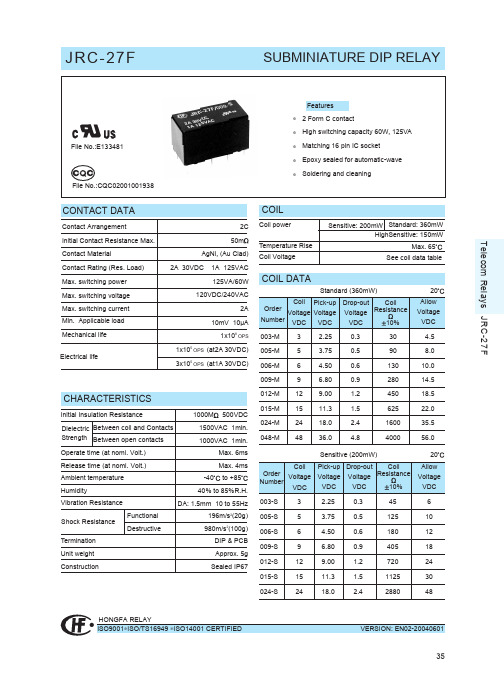
CONTACT DATA
Contact Arrangement Initial Contact Resistance Max. Contact Material Contact Rating (Res. Load) Max. switching power Max. switching voltage Max. switching current Min. Applicable load Mechanical life 1x10 Electrical life 3x10
(at2A 30VDC) (at1A 30VDC)
CHARACTERISTICS
Initial Insulation Resistance Dielectric Between coil and Contacts Strength Between open contacts Operate time (at nomi. Volt.) Release time (at nomi. Volt.) Ambient temperature Humidity Vibration Resistance Shock Resistance Termination Unit weight Construction Functional Destructive -40 1000M 500VDC 1500VAC 1min. 1000VAC 1min. Max. 6ms Max. 4ms to +85
元器件交易网
JRC-27F
SUBMINIATURE DIP RELAY
Features * 2 Form C contact * High switching capacity 60W, 125VA File No.:E133481 * Matching 16 pin IC socket * Epoxy sealed for automatic-wave * Soldering and cleaning File No.:CQC02001001938
集成电路中文名称大全

集成电路中文名称大全型号规格性能说明型号规格性能说明SN74LSOO 四2输入与非门SN74LSO1 四2输入与非门SN74LSO2 四2输入与非门SN74LS03 四2输入与非门SN74LS04 六反相器SN74LS05 六反相器SN74LS06 六反相缓冲器/驱动器SN74LS07 六缓冲器/驱动器SN74LS08 四2输入与非门SN74LS09 四2输入与非门SN74LS10 三3输入与非门SN74LS11 三3输入与非门SN74LS12 三3输入与非门SN74LS13 三3输入与非门SN74LS14 六反相器.斯密特触发SN74LS15 三3输入与非门SN74LS16 六反相缓冲器/驱动器SN74LS17 六反相缓冲器/驱动器SN74LS20 双4输入与门SN74LS21 双4输入与门SN74LS22 双4输入与门SN74LS25 双4输入与门SN74LS26 四2输入与非门SN74LS27 三3输入与非门SN74LS28 四输入端或非缓冲器SN74LS30 八输入端与非门SN74LS32 四2输入或门SN74LS33 四2输入或门SN74LS37 四输入端与非缓冲器SN74LS38 双2输入与非缓冲器SN74LS40 四输入端与非缓冲器SN74LS42 BCD-十进制译码器SN74LS47 BCD-七段译码驱动器SN74LS48 BCD-七段译码驱动器SN74LS49 BCD-七段译码驱动器SN74LS51 三3输入双与或非门SN74LS54 四输入与或非门SN74LS55 四4输入与或非门SN74LS63 六电流读出接口门SN74LS73 双J-K触发器SN74LS74 双D触发器SN74LS75 4位双稳锁存器SN74LS76 双J-K触发器SN74LS78 双J-K触发器SN74LS83 双J-K触发器SN74LS85 4位幅度比较器SN74LS86 四2输入异或门SN74LS88 4位全加器SN74LS90 4位十进制波动计数器SN74LS91 8位移位寄存器SN74LS92 12分频计数器SN74LS93 二进制计数器SN74LS96 5位移位寄存器SN74LS95 4位并入并出寄存器SN74LS109 正沿触发双J-K触发器SN74LS107 双J-K触发器SN74LS113 双J-K负沿触发器SN74LS112 双J-K负沿触发器SN74LS121 单稳态多谐振荡器SN74LS114 双J-K负沿触发器SN74LS123 双稳态多谐振荡器SN74LS122 单稳态多谐振荡器SN74LS125 三态缓冲器SN74LS124 双压控振荡器SN74LS131 3-8线译码器SN74LS126 四3态总线缓冲器SN74LS133 13输入与非门SN74LS132 二输入与非触发器SN74LS137 地址锁存3-8线译码器SN74LS136 四异或门SN74LS139 双2-4线译码-转换器SN74LS138 3-8线译码/转换器SN74LS147 10-4线优先编码器SN74LS145 BCD十进制译码/驱动器SN74LS153 双4选1数据选择器SN74LS148 8-3线优先编码器SN74LS155 双2-4线多路分配器SN74LS151 8选1数据选择器SN74LS157 四2选1数据选择器SN74LS154 4-16线多路分配器SN74LS160 同步BDC十进制计数器SN74LS156 双2-4线多路分配器SN74LS162 同步BDC十进制计数器SN74LS158 四2选1数据选择器SN74LS164 8位串入并出移位寄存SN74LS161 4位二进制计数器SN74LS166 8位移位寄存器SN74LS163 4位二进制计数器SN74LS169 4位可逆同步计数器SN74LS165 8位移位寄存器SN74LS172 16位多通道寄存器堆SN74LS168 4位可逆同步计数器SN74LS174 6D型触发器SN74LS170 4x4位寄存器堆SN74LS176 可预置十进制计数器SN74LS173 4D型寄存器SN74LS182 超前进位发生器SN74LS175 4D烯触发器SN74LS189 64位随机存储器SN74LS181 运算器/函数发生器SN74LS191 二进制同步可逆计数器SN74LS183 双进位保存全价器SN74LS193 二进制可逆计数器SN74LS190 同步BCD十进制计数器SN74LS195 并行存取移位寄存器SN74LS192 BCD-同步可逆计数器SN74LS197 可预置二进制计数器SN74LS194 双向通用移位寄存器SN74LS238 3-8线译码/多路转换器SN74LS196 可预置十进制计数器SN74LS241 八缓冲/驱动/接收器SN74LS221 双单稳态多谐振荡器SN74LS243 四总线收发器SN74LS240 八缓冲/驱动/接收器SN74LS245 八总线收发器SN74LS242 四总线收发器SN74LS248 BCD-七段译码驱动器SN74LS244 八缓冲/驱动/接收器SN74LS251 三态8-1数据选择器SN74LS247 BCD-七段译码驱动器SN74LS256 双四位选址锁存器SN74LS249 BCD-七段译码驱动SN74LS258 四2选1数据选择器SN74LS253 双三态4-1数据选择器SN74LS260 双5输入或非门SN74LS257 四3态2-1数据选择器SN74LS266 四2输入异或非门SN74LS259 8位可寻址锁存器SN74LS275 七位树型乘法器SN74LS261 2x4位二进制乘发器SN74LS279 四R-S触发器SN74LS273 八进制D型触发器SN74LS283 4位二进制全加器SN74LS276 四J-K触发器SN74LS293 4位二进制计数器SN74LS280 9位奇偶数发生校检器SN74LS365 六缓冲器带公用启动器SN74LS290 十进制计数器SN74LS367 六总线三态输出缓冲器SN74LS295 4位双向通用移位寄存器SN74LS373 8D锁存器SN74LS366 六缓冲器带公用启动器SN74LS375 4位双稳锁存器SN74LS368 六总线三态输出反相器SN74LS386 四2输入异或门SN74LS374 8D触发器SN74LS393 双4位二进制计数器SN74LS377 8位单输出D型触发器SN74LS574 8位D型触发器SN74LS390 双十进制计数器SN74LS684 8位数字比较器SN74LS573 8位三态输出D型锁存器SN74HC11 三3输入与门SN74LS670 8位数字比较器SN7404 六反相器SN74HC00 四2输入与非门SN7406 六反相缓冲器/驱动器SN74HC02 四2输入或非门SN7407 六缓冲器/驱动器SN74HC03 四2输入或非门SN7414 六缓冲器/驱动器SN74HC04 六反相器SN7416 六反相缓冲器/驱动器SN74HC05 六反相器SN7440 六反相缓冲器/驱动器SN74HC08 四2输入与门SN7497 六反相缓冲器/驱动器SN74HC10 三3输入与非门74F00 高速四2输入与非门SN74HC14 六反相器/斯密特触发74F02 高速四2输入或非门SN74HC20 双四输入与门74F04 高速六反相器SN74HC21 双四输入与非门74F08 高速四2输入与门SN74HC27 三3输入与非门74F10 高速三3输入与门SN74HC30 八输入端与非门74F14 高速六反相斯密特触发SN74HC32 四2输入或门74F32 高速四2输入或门SN74HC42 BCD十进制译码器74F38 高速四2输入或门SN74HC73 双J-K触的器74F74 高速双D型触发器SN74HC74 双D型触发器74F86 高速四2输入异或门SN74HC76 双J-K触的器74F139 高速双2-4线译码/驱动器SN74HC86 四2输入异或门74F151 高速双2-4线译码/驱动器SN74HC107 双J-K触发器74F153 高速双4选1数据选择器SN74HC113 双J-K负沿触发器74F157 高速双4选1数据选择器SN74HC123 双稳态多谐振荡器74F161 高速6D型触发器SN74HC125 三态缓冲器74F174 高速6D型触发器SN74HC126 四三态总线缓冲器74F175 高速4D型触发器SN74HC132 二输入与非缓冲器74F244 高速八总线3态缓冲器SN74HC137 二输入与非缓冲器74F245 高速八总线收发器SN74HC138 3-8线译码/解调器74F373 高速8D锁存器SN74HC139 双2-4线译码/解调器SN74HCT04 六反相器SN74HC148 8选1数据选择器CD4001 4二输入或非门SN74HC151 双4选1数据选择器CD4002 双4输入或非门SN74HC154 4-16线多路分配器CD4006 18位静态移位寄存器SN74HC157 四2选1数据选择器CD4007 双互补对加反相器SN74HC161 4位二进制计数器CD4009 六缓冲器/转换-倒相SN74HC163 4位二进制计数器CD4010 六缓冲器/转换-正相SN74HC164 8位串入并出移位寄存器CD4011 四2输入与非门SN74HC165 8位移位寄存器CD4012 双4输入与非门SN74HC173 4D型触发器CD4013 置/复位双D型触发器SN74HC174 6D触发器CD4014 8位静态同步移位寄存SN74HC175 4D型触发器CD4015 双4位静态移位寄存器SN74HC191 二进制同步可逆计数器CD4016 四双向模拟数字开关SN74HC221 双单稳态多谐振荡器CD4017 10译码输出十进制计数器SN74HC238 3-8线译码器CD4018 可预置1/N计数器SN74HC240 八缓冲器CD4019 四与或选择门SN74HC244 八总线3态输出缓冲器CD4020 14位二进制计数器SN74HC245 八总线收发器CD4021 8位静态移位寄存器SN74HC251 三态8-1数据选择器CD4022 8译码输出8进制计数器SN74HC259 8位可寻址锁存器CD4023 三3输入与非门SN74HC266 四2输入异或非门CD4024 7位二进制脉冲计数器SN74HC273 8D型触发器CD4025 三3输入与非门SN74HC367 六缓冲器/总线驱动器CD4026 十进制/7段译码/驱动SN74HC368 六缓冲器/总线驱动器CD4027 置位/复位主从触发器SN74HC373 8D锁存器CD4028 BCD十进制译码器SN74HC374 8D触发器CD4029 4位可预置可逆计数器SN74HC393 双4位二进制计数器CD4030 四异或门SN74HC541 8位三态输出缓冲器CD4031 64位静态移位寄存器SN74HC573 8位三态输出D型锁存器CD4032 三串行加法器SN74HC574 8D型触发器CD4033 十进制计数器/7段显示SN74HC595 8位移位寄存器/锁存器CD4034 8位静态移位寄存器SN74HC4028 7级二进制串行加数器CD4035 4位并入/并出移位寄存器SN74HC4046 锁相环CD4038 3位串行加法器SN74HC4050 六同相缓冲器CD4040 12位二进制计数器SN74HC4051 8选1模拟开关CD4041 四原码/补码缓冲器SN74HC4053 三2选1模拟开关CD4042 四时钟D型锁存器SN74HC4060 14位计数/分频/振荡器CD4043 四或非R/S锁存器SN74HC4066 四双相模拟开关CD4044 四与非R/S锁存器SN74HC4078 3输入端三或门CD4046 锁相环SN74HC4511 7段锁存/译码驱动器CD4047 单非稳态多谐振荡器SN74HC4520 双二进制加法计数器CD4048 可扩充八输入门CD4502 可选通六反相缓冲器CD4049 六反相缓冲/转换器CD4503 六同相缓冲器CD4050 六正相缓冲/转换器CD4504 六电平转换器CD4051 单8通道多路转换/分配CD4508 双4位锁存器CD4052 双4通道多路转换/分配CD4510 BCD可预置可逆计数器CD4053 三2通道多路转换/分配CD4511 BCD7段锁存/译码/驱动CD4056 7段液晶显示译码/驱动CD4512 8通道数据选择器CD4060 二进制计数/分频/振荡CD4513 BCD7段锁存/译码/驱动CD4063 四位数值比较器CD4514 4-16线译码器CD4066 四双相模拟开管CD4515 4-16线译码器CD4067 16选1模拟开关CD4518 双BCD加法计数器CD4068 8输入端与非/与门CD4520 双二进制加法计数器CD4069 六反相器CD4521 24位分频器CD4070 四异或门CD4522 可预置BCD1/N计数CD4071 四2输入或门CD4526 可预置二进制1/N计数CD4072 双四输入或门CD4527 BCD系数乘发器CD4073 三3输入与门CD4528 双单稳态触发器CD4075 三3输入与门CD4531 12位奇偶校验电路CD4076 4位D型寄存器CD4532 8位优先编码器CD4077 四异或非门CD4538 双精密单稳态触发器CD4078 八输入或/或非门CD4539 双四路输据选择器CD4081 四输入与门CD4541 可编程振荡/计时器CD4082 双4输入与门CD4543 7段锁存/译码/驱动CD4085 双2组2输入与或非门CD4553 3位BCD计数器CD4086 可扩展2输入与或非门CD4555 双4选1译码器CD4093 四与非斯密特触发器CD4556 双4选1译码器CD4094 8位移位/贮存总线寄存CD4557 1-64位可变长度寄存器CD4096 3输入J-K触发器CD4558 BCD-7段译码器CD4098 双单稳态触发器CD4560 BCD码加法器CD4099 8位可寻址锁存器CD4561 BCD转换成9的补码输出CD40103 同步可预置减法器CD4566 工业定时基准发生器CD40106 六斯密特触发器CD4569 双4位可编程1/NBCDCD40107 双2输入与非缓冲/驱动CD4583 双斯密特触发器CD40110 计数/译码/锁存/驱动CD4584 4斯密特触发器CD40174 6D触发器CD4585 4位数值比较器CD40175 4D触发器CD4599 8位总线相容寻址锁存器CD40192 BCD可预置可逆计数器MC145106 频率合成器CD40193 二进制可预置可逆计数器MC145026 遥控编码器CD40194 4位双相移位寄存器MC145027 译码器4N25 晶体管输出LM24J 四运放(军用级)4N25MC 晶体管输出LM148J 通用四运放4N26 晶体管输出LM1875T 无线电控制/接收器4N27 晶体管输出LM224J 四运放(工业级)4N28 晶体管输出258N 分离式双电源双运放4N29 达林顿输出LM2901N 四电压比较器4N30 达林顿输出LM2904N 四运放4N31 达林顿输出LM301AN 通用运算放大器4N32 达林顿输出LM308N 单比较器4N33 达林顿输出LM311P 单比较器4N33MC 达林顿输出LM317L 可调三端稳压器/100mA4N35 达林顿输出LM317T 可调三端稳压器/1.5A4N36 晶体管输出LM317K 可调三端稳压器/3A4N37 晶体管输出LM318 高速宽带运放4N38 晶体管输出LM324K 通用四运放4N39 可控硅输出LM331N V-F/F-V转换器6N135 高速光耦晶体管输出LM336-2.5V 基准电压电路6N136 高速光耦晶体管输出LM336 5V 基准电压电路6N137 高速光耦晶体管输出LM337T 基准电压电路1A6N138 达林顿输出LM338K 可调三端稳压器5A6N139 达林顿输出LM339N 四比较器MOC3020 可控硅驱动输出LM348N 四741运放MOC3021 可控硅驱动输出LM358N 低功耗双运放MOC3023 可控硅驱动输出LM361N 高速差动比较器MOC3030 可控硅驱动输出LM386N 声频功率放大器MOC3040 过零触发可控硅输出LM3914N 十段点线显示驱动MOC3041 过零触发可控硅输出LM393N 低功耗低失调双比较器MOC3061 过零触发可控硅输出LM399H 精密基准源(6.9) MOC3081 过零触发可控硅输出LM723CN 可调正式负稳压器TLP521-1 单光耦LM733CN 视频放大器TLP521-2 双光耦LM741J 单运放TLP521-4 四光耦LM741CN 双运放TLP621 四光耦OP07 低噪声运放TIL113 达林顿输出OP27 超低噪声精密运放TIL117 TLL逻辑输出OP37 超低噪声精密运放PC814 单光耦TL062 低功耗JEFT输入双运放PC817 单光耦TL072 低噪声JEFTH11A2 晶体管输出ULN2003 周边七段驱动陈列H11D1 高压晶体管输出ULN2004 周边七段驱动陈列H11G2 电阻达林顿输出ULN2803 周边八段驱动陈列LF347N 宽带JFET输入四运放ULN2804 周边八段驱动陈列LF351N 宽带JFET输入运放ICL7106 3位ADC/驱动LCDLF353N JFET输入宽带运放ICL7107 3位半ADC/驱动LEDLF355N JFET输入运放ICL7109 4位半ADC/驱动LEDLF357N JFET宽带非全裣运放ICL7129 4位半ADC/LCD驱动LF398N 采样/保持电路ICL7135 ADC/LCD驱动BCD输出LF412N 低偏差飘移输入运放ICL7136 3位半CMOSADC/LCD驱动MC1377 彩色电视编码器ICL7218 CMOS低功耗运算放大器MC1403 精密电压基准源(2.5) ICL7650 整零运放斩波MC1413 周边七段驱动阵列ICL7652 整零运放斩波MC1416 周边七段驱动陈列ICL7660 CMOS直流-直流转换器MC14409 二进制脉冲拨号器ICL8038 函数信号发生器MC14433 3位半A/D转换器ICL8049 反对数放大器MC14489 多字符LED显示驱动器CA3140 单BIMOS运行MC145026 编码器CA3240 单BIMOS运行VD5026 编码器UC3842 WM电流型控制器MC145027 译码器UC3845 PWM电流型控制器VD5027 译码器DS12887 非易失实时时钟芯片MC145028 译码器L3845 中继接口电路MC145030 编码译码器SG3524 PWM解调调制器MC145106 频率合成器SG3525 PWM解调调制器MC145146 4位数据总线20106 前置放大器NE521 高速双差分比较器TCM5087 双音调发生器NE5532 双运放MM5832 实时钟电路NE5534 双运放TC14433 3位半A/D转换器NE555N 单运放TC232 并行/串行接口电路NE555J 时基电路军品极TC7106 3位半ADC/LCD驱动NE556 双级型双时基电路TC7107 3位半ADC/LED驱动NE564 锁相环TC7116 3位半ADC/LCD驱动带保NE565 锁相环TC7129 4位半ADC/LCDNE567 音调译码器TC7135 4位半ADC/LCD,BCD输出NE592 视频放大器TC7650 整零运放斩波MT8814 8x12模拟交换矩阵75107 四差分线驱动器MT8816 8x模拟交换矩阵75174 四差分线驱动器MT8870 综合DTMF接收器75175 三态四差分接收器MT8870 综合DTMF接收器75176 差分总线接收器MT8880 综合DTMF发生接收器75188 四线驱动器24LC01 128x8串行EEPROM 75189 四线驱动器24LC02 256x8串行EEPROM 75451 双外围驱动器24LC04 512x8串行EEPROM 75452 双外围驱动器93LC46 64x16串行EEPROM PAL16L8 FLASH200门93LC56 256x16串行EEPROM PALCE16V8-25 FLASH200门93LC66 512x8 256x16 EEPROM PALCE16V8-25JC FLASH200门(贴片)PIC16C52 384x12 单片机ATF16V8-25PC FLASH200门PIC16C54 512x12 单片机GAL16V8-25LP FLASH200门PCI16C56 512x12 单片机GAL16V8-25LPI 工业级FLASH200门PIC16C57 2048x12 单片机GALV8-20LD 军品级FLASH200门AT24C01 128x8串行EEPROM GAL16V8-15LP 军品级FLASH200门AT24C02 256x8串行EEPROM GAL16V8-15LPI 工业级FLASH200门AT24C04 512x8串行EEPROM PALCF20V8-25PC FLASH300门AT24C16 2Kx8串行EEPROM A TF20V8-25PC FLASH300门AT93C46 64x16串行EEPROM GAL20V8-25LP FLASH300门AT93C56 256x16串行EEPROM GAL20V8-25LPI 工业级FLASH门ATF16V8 FLASH200门GAL20V8-20LD 军品级门ATF20V8 FLASH300门高速GAL20V8-15LP 军品级门ATF22V10 FLASH500门高速低电流GAL20V8-15LPI 工业级FLASH门AT28C16 2Kx8CMOS并行EEPROM ATF22C10-25PC FLASH500门高速低电流AT28C17 2Kx8CMOS并行EEPROM ATF22C10-25PC FLASH500门高速低电流AT28C64 8Kx8并行EEPROM GAI22V10-25LP FLASH500门高速低电流AT28C256 32Kx8并行EEPROM PALCE22V10-15JC FLASH500门高速低电流AT28F010 128Kx8并行EEPROM 2716 8Kx8 NMOS EPROMA29C040 512Kx8 FLASH EEPROM 27C16 2Kx8 NMOS EPROMHM6116 2Kx8 CMOS 静态PAM 2732 4Kx8 NMOS EPROMHY6264 8Kx8 CMOS 静态RAM 27C32 4Kx8 NMOS EPROMHM6264 8Kx8 CMOS 静态RAM 2764F 8Kx8 NMOS EPROMIS62C64 8Kx8 高速CMOS 静态RAM 27C64F 8Kx8 NMOS EPROMHY62256 32Kx8 CMOS 静态RAM 2764ST 8Kx8 NMOS EPROMHM62256 32Kx8 CMOS 静态RAM 27C64ST 8Kx8 NMOS EPROMHM628128 128Kx8 CMOS 静态RAM 27C64NS 8Kx8 NMOS EPROMHM628256 256Kx8 CMOS 静态RAM 27128 16Kx8 NMOS EPROMHM628512 512Kx8 CMOS 静态RAM 27C128 16Kx8 NMOS EPROMHM628512 512Kx8 CMOS 静态RAM 27256 32Kx8 NMOS EPROMZ80 CP CTC PIO S10 27C256 32Kx8 NMOS EPROMLD8031AH 8位微处理器工业级MD27C256 16Kx8 CMOS EPROM8031 8位微处理器27HC256-45 16Kx8 高速CMOS EPROM80C31 8位CMOST微处理器27512 64Kx8 NMOS EPROM80C31NT 8位CMOST微处理器27C512 64Kx8 NMOS EPROMN80C31BH 8位CMOST微处理器贴片MD27C512 64Kx8 NMOS EPROMLD80C31BH 8位CMOST微处理器27HC512-45 64Kx 高速CMOS EPROM MD80C31BH 8位CMOST微处理器27C010 128Kx8 CMOS EPROM8032 8位微处理器27HC010-30 128Kx8 CMOS EPROMLD8032AH 8位CMOST微处理器27C020 256Kx8 CMOS EPROM80C32 8位CMOS微控制器27C040 512Kx8 CMOS EPROM8039 8位微控制器27HC040-30 512Kx8 CMOS EPROM80C39 8位微控制器27C080 1024Kx8 CMOS EPROM8051 8位微控制器2816 2Kx8 并行EEPROM80C51 8位CMOS微控制器28C16 2Kx8 CMOS 并行EEPROM80C552 8位微控制器2817 2Kx8 并行EEPROM80C552新8位微控制器28C17 2Kx8 CMOS 并行EEPROM8080 8位微处理器2864 8Kx8 并行EEPROM8085 8位NMOS微处理器28C64 8Kx8 CMOS 并行EEPROM80C85 8位NMOS微处理器28C64B15JC 8Kx8 CMOS 并行EEPROM 8086 16位NMOS微处理器28C256 32Kx8 CMOS 并行EEPROM80C86 CMOS 16位微处理器28F010 128Kx 高速并行EEPROM8087 数值协处理器2810 128Kx 高速并行EEPROM8088 8位HMOS微处理器28F020 256Kx 高速并行EEPROM80C88 CMOS 8位HMOS微处理器28F020-150 256Kx 高速并行EEPROM 8097 16位单片机28F256 32Kx 高速并行EEPROM8098 准16位微控制器28F256 32Kx 高速并行EEPROM8155 通用接口电路29C010 128Kx8 FLASH EEPROM81C55 CMOS通用接口电路29C040 512Kx8 FLASH EEPROM8212 时钟发生器和驱动器29F040-90 512Kx8 FLASH EEPROM8228 系统控制和总线驱动器AD1674KN 12位2KHZ带采保ADC8237 DMA控制器AD202JY 小型2KHZ隔离放大器82C37 CMOS DMA 控制器AD232JN 线路驱动接收器8243 扩展器AD521JD 电阻设置精密仪放器82C43 CMOS I/O扩展器AD574AJD 12位数模转换器8250 异步通信接口电路AD590JH 宽温度范围传感器82C50 CMOS 异步通信接口电路AD624AD 精密仪表放大器8251 串行通信接口电路AD650JN 低线性误差压频转换器MD8251A 异步通信接口电路ADC0804 8位A/D转换器82C51 CMOS 异步通信接口电路ADC0808 8位A/D转换器8253 可编程区间计数器ADC0809 8位A/D转换器82C53 CMOS 可编程区间计数器ADC0820 8位A/D转换器8254 可编程间隔定时器DAC0808 8位A/D转换器83C54 CMOS 可编程间隔定时器DAC0832 8位A/D转换器LP82C54 CMOS 可编程间隔定时器DAC1210 12位A/D转换器8255 可编程外围并行接口电路MAX1487CPA ESD保护RS-485MD8255A 可编程外围并行接口电路MAX1202CPE RS-232接口电路82C55 CMOS 可编程外围并行接口MAX232CPA RS-232接口电路8257 可编程DMA控制器MAX485CPA RS-485接口电路8259 可编程中段控制器MAX488CPA RS-485接口电路82C59 CMOS 可编程中段控制器MAX706CPA UP监控电路8279 可编程键盘显示器接口电路MAX7219CNA 8位显示驱动器82C79 CMOS 8279 MAX756CPA UP监控电路8282 8位锁存器MAX483 UP监控电路8283 8位锁存器TDA1521 低电平检测宽带放大器8284 时钟发生器和驱动器TDA2003A 单功率放大器5-10W 8286 8位总线收发器TDA2030A 单功率放大器>10W8287 8位总线收发器TDA2822 桑苗双功率放大器8288 总线控制器87C552 8位微控制器82C88 CMOS 总线控制器89C1051PC 1K8位FLASH单片机8748 8位微控制器89C2051PC 2K8位FLASH单片机8749 8位微控制器89C2051PI 2K8位FLASH单片机8751 8位微控制器89C51PC 4K8位FLASH单片机87C51 CMOS 8位控制器89C51PI 4K8位FLASH单片机87C51FA CMOS 8位微控制器89C52PC 2K8位FLASH单片机87C52 87C51加强型89C52PI 2K8位FLASH单片机89C55PC 20Kx8位89C52JC 2K8位FLASH单片机。
LFHFUHF都分别代表什么
LF, HF, UHF都分别代表什么?和我们听的收音机道理一样,射频标签和阅读器也要调制到相同的频率才能工作。
LF,HF,UHF就对应着不同频率的射频。
LF代表低频射频,在125KHz左右,HF代表高频射频,在13.56MHz左右,UHF代表超高频射频,在860至960MHz范围之内。
对一个RFID系统来说,它的频段概念是指读写器通过天线发送、接收并识读的标签信号频率范围。
从应用概念来说,射频标签的工作频率也就是射频识别系统的工作频率,直接决定系统应用的各方面特性。
在RFID系统中,系统工作就像我们平时收听调频广播一样,射频标签和读写器也要调制到相同的频率才能工作。
射频标签的工作频率不仅决定着射频识别系统工作原理(电感耦合还是电磁耦合)、识别距离,还决定着射频标签及读写器实现的难易程度和设备成本。
RFID 应用占据的频段或频点在国际上有公认的划分,即位于ISM波段。
典型的工作频率有:125kHz、133kHz、13.56MHz、27.12MHz、433MHz、902MHz~928MHz、2.45GHz、5.8GHz等。
按照工作频率的不同,RFID标签可以分为低频(LF)、高频(HF)、超高频(UHF)和微波等不同种类。
不同频段的RFID工作原理不同,LF和HF频段RFID 电子标签一般采用电磁耦合原理,而UHF及微波频段的RFID一般采用电磁发射原理。
目前国际上广泛采用的频率分布于4种波段,低频(125KHz)、高频(13.54MHz)、超高频(850MHz~910MFz)和微波(2.45GHz)。
每一种频率都有它的特点,被用在不同的领域,因此要正确使用就要先选择合适的频率。
低频段射频标签,简称为低频标签,其工作频率范围为30kHz~300kHz。
典型工作频率有125KHz和133KHz。
低频标签一般为无源标签,其工作能量通过电感耦合方式从阅读器耦合线圈的辐射近场中获得。
低频标签与阅读器之间传送数据时,低频标签需位于阅读器天线辐射的近场区内。
集成电路英文代码对照

集成电路英文代码及中文对照〔一〕我的文摘2021-11-21 11:32:53 阅读111 评论0 字号:大中小订阅产品名称型号规格性能说明LMLM24J 四运放(军用级)LM148J 通用四运放LM1875T 无线电控制/接收器LM224J 四运放(工业级)LM258N 别离式双电源双运放LM2901N 四电压比拟器LM2904N 四运放LM301AN 通用运算放大器LM308N 单比拟器LM311P 单比拟器LM317L 可调三端稳压器/100mALM317TLM317K 可调三端稳压器/3ALM318 高速宽带运放LM324K 通用四运放LM331N V-F/F-V转换器基准电压电路LM336 5V 基准电压电路LM337T 基准电压电路1ALM338K 可调三端稳压器5ALM339N 四比拟器LM348N 四741运放LM358N 低功耗双运放LM361N 高速差动比拟器LM386N 声频功率放大器LM3914N 十段点线显示驱动LM393N 低功耗低失调双比拟器LM399H 精细基准源(6.9)LM723CN 可调正式负稳压器LM733CN 视频放大器LM741J 单运放LM741CN 双运放NENE521 高速双差分比拟器NE5532 双运放NE5534 双运放NE555N 单运放NE555J 时基电路军品极NE556 双级型双时基电路NE564 锁相环NE565 锁相环NE567 音调译码器NE592 视频放大器OPOP07 低噪声运放OP27 超低噪声精细运放OP37 超低噪声精细运放光电耦合4N25 晶体管输出4N25MC 晶体管输出4N26 晶体管输出4N27 晶体管输出4N28 晶体管输出4N29 达林顿输出4N30 达林顿输出4N31 达林顿输出4N32 达林顿输出4N33 达林顿输出4N33MC 达林顿输出4N35 达林顿输出4N36 晶体管输出4N37 晶体管输出4N38 晶体管输出4N39 可控硅输出6N135 高速光耦晶体管输出6N136 高速光耦晶体管输出6N137 高速光耦晶体管输出6N138 达林顿输出6N139 达林顿输出MOC3020 可控硅驱动输出MOC3021 可控硅驱动输出MOC3023 可控硅驱动输出MOC3030 可控硅驱动输出MOC3040 过零触发可控硅输出MOC3041 过零触发可控硅输出MOC3061 过零触发可控硅输出MOC3081 过零触发可控硅输出TLP521-1 单光耦TLP521-2 双光耦TLP521-4 四光耦TLP621 四光耦TIL113 达林顿输出TIL117 TLL逻辑输出PC814 单光耦PC817 单光耦H11A2 晶体管输出H11D1 高压晶体管输出H11G2 电阻达林顿输出LFLF347N 宽带JFET输入四运放LF351N 宽带JFET输入运放LF353N JFET输入宽带运放LF355N JFET输入运放LF357N JFET宽带非全裣运放LF398N 采样/保持电路LF412N 低偏向飘移输入运放MCMC1377 彩色电视编码器MC1403 精细电压基准源(2.5)MC1413 周边七段驱动阵列MC1416 周边七段驱动陈列MC14409 二进制脉冲拨号器MC14433 3位半A/D转换器MC14489 多字符LED显示驱动器MC145026 编码器VD5026 编码器MC145027 译码器VD5027 译码器MC145028 译码器MC145030 编码译码器MC145106 频率合成器MC145146 4位数据总线TLTL062 低功耗JEFT输入双运放TL072 低噪声JEFTTL082TL084TL431TL494ULNULN2003 周边七段驱动陈列ULN2004 周边七段驱动陈列ULN2803 周边八段驱动陈列ULN2804 周边八段驱动陈列ICLICL7106 3位ADC/驱动LCDICL7107 3位半ADC/驱动LEDICL7109 4位半ADC/驱动LEDICL7129 4位半ADC/LCD驱动ICL7135 ADC/LCD驱动BCD输出ICL7136 3位半CMOSADC/LCD驱动ICL7218 CMOS低功耗运算放大器ICL7650 整零运放斩波ICL7652 整零运放斩波ICL7660 CMOS直流-直流转换器ICL8038 函数信号发生器ICL8049 反对数放大器CACA3140 单BIMOS运行CA3240 单BIMOS运行UCUC3842 WM电流型控制器UC3845 PWM电流型控制器DSDS12887 非易失实时时钟芯片L3845 中继接口电路SGSG3524 PWM解调调制器SG3525 PWM解调调制器20216 前置放大器MTMT8814 8x12模拟交换矩阵MT8816 8x模拟交换矩阵MT8870 综合DTMF接收器MT8870 综合DTMF接收器MT8880 综合DTMF发生接收器MIC24LC01 128x8串行EEPROM24LC02 256x8串行EEPROM24LC04 512x8串行EEPROM24LC16 2Kx8串行EEPROM93LC46 64x16串行EEPROM93LC56 256x16串行EEPROM93LC66 512x8 256x16 EEPROMPIC16C52 384x12 单片机PIC16C54 512x12 单片机PCI16C56 512x12 单片机PIC16C57 2048x12 单片机ATAT24C01 128x8串行EEPROMAT24C02 256x8串行EEPROMAT24C04 512x8串行EEPROMAT24C16 2Kx8串行EEPROMAT93C46 64x16串行EEPROMAT93C56 256x16串行EEPROMATF16V8 FLASH200门ATF20V8 FLASH300门高速ATF22V10 FLASH500门高速低电流AT28C16 2Kx8CMOS并行EEPROMAT28C17 2Kx8CMOS并行EEPROMAT28C64 8Kx8并行EEPROMAT28C256 32Kx8并行EEPROMAT28F010 128Kx8并行EEPROMA29C040 512Kx8 FLASH EEPROMHM6116 2Kx8 CMOS 静态PAMHY6264 8Kx8 CMOS 静态RAMHM6264 8Kx8 CMOS 静态RAMIS62C64 8Kx8 高速CMOS 静态RAMHY62256 32Kx8 CMOS 静态RAMHM62256 32Kx8 CMOS 静态RAMHM628128 128Kx8 CMOS 静态RAMHM628256 256Kx8 CMOS 静态RAMHM628512 512Kx8 CMOS 静态RAMHM628512 512Kx8 CMOS 静态RAM TCMTCM5087 双音调发生器MM5832 实时钟电路TCTC14433 3位半A/D转换器TC232 并行/串行接口电路TC7106 3位半ADC/LCD驱动TC7107 3位半ADC/LED驱动TC7116 3位半ADC/LCD驱动带保TC7129 4位半ADC/LCDTC7135 4位半ADC/LCD,BCD输出TC7650 整零运放斩波7575107 四差分线驱动器75174 四差分线驱动器75175 三态四差分接收器75176 差分总线接收器75188 四线驱动器75189 四线驱动器75451 双外围驱动器75452 双外围驱动器集成电路英文代码及中文对照〔二〕我的文摘2021-11-21 11:37:11 阅读191 评论0 字号:大中小订阅。
LG 27MD5KL 电视机用户手册说明书

OWNER’S MANUAL(For Mac)Please read this manual carefully before operating your set and retain it for future reference.27MD5KL27MD5KLBCopyright © 2019 LG Electronics Inc. All Rights Reserved.ENGLISHLICENSEEach model has different licenses. Visit for more information on the license.Thunderbolt and the Thunderbolt logo are trademarks of IntelCorporation or its subsidiaries in the U.S. and/or other countries.Mac and the Mac logo are trademarks of Apple Inc., registered inthe U.S. and other countries.*CONTENTSLICENSE ------------------------------------------------2IMPORTANT PRECAUTIONS ---------------------------3OPEN SOURCE SOFTWARE NOTICE INFORMATION ---6ASSEMBLING AND PREPARING -----------------------6MAKING CONNECTIONS ------------------------------23TROUBLESHOOTING ----------------------------------26PRODUCT SPECIFICATION ----------------------------2823ENGLISHIMPORTANT PRECAUTIONSPlease read these safety precautions carefully before using the product.WARNINGFailure to follow those warnings may result in death, serious injury or damage to the product or other property.Precautions to the AC Adapter and Electrical PowerWARNING•If water or any foreign substance goes inside the product (TV, monitor, power cord, or AC adapter), disconnectthe power cord immediately and contact the service center.Otherwise, this may cause a fire or electric shock due to damage to the product.•Do not touch the power plug or AC adapter with wet hands. If the pins of the plug are wet or dusty, wipe and dry them before use.Otherwise, this may cause a fire or electric shock.•Make sure to completely insert the power cord into the AC adapter.If loosely connected, the poor connection may cause a fire or electric shock.•Be sure to use power cords and AC adapters provided or approved by LG Electronics, Inc.The use of non-approved products may cause a fire or electric shock.•When unplugging the power cord, always pull it by the plug. Do not bend the power cord with excessive force.The power line can be damaged, which may cause electric shock or fire.•Be careful not to step or place heavy objects (electronic appliances, clothing, etc.) on the power cord or AC adapter. Be careful not to damage the power cord or AC adapter with sharp objects.Damaged power cords may cause a fire or electric shock.•Never disassemble, repair or modify the power cord or AC adapter.This may cause a fire or electric shock.•Use only the power cord supplied with the unit or another manufacturer's authorized cord.Failure to do so may result in fire or electrical shock or damage to the product. •Use only a properly grounded plug and receptacle.If you do not you may be electrocuted or injured. Or the product might be damaged. •Do not use a damaged or loose plug.This may cause electrical shock or fire.•Operate the display only from a power source(i.e. voltage) indicated in the product specification.Otherwise the product can be damaged, fire can occur or you may be electrocuted. If you are not sure what type of power supply you have, consult a certified electrician.•In the presence of thunder and lightning, never touch the power cord and signal cable because it can be very dangerous.It can cause electric shock.•Do not connect several extension cords, electrical appliances or electrical heaters to a single outlet. Use a power bar with a grounding terminal designed for exclusive use with the computer.A fire can break out due to overheating.•Do not touch the power plug with wet hands. Additionally, if the cord pin is wet or covered with dust, dry the power plug completely or wipe dust off before plugging in the cord.You may be electrocuted due to excess moisture.•If you don’t intend to use the product for a long time, unplug the power cable from the product.Covering dust can cause a fire, or insulation deterioration can cause electric leakage, electric shock or fire. •Insert the power plug firm so it cannot come loose.A loose connection can cause fire.•Do not insert metal or other conductive materials into the product openings. Additionally, do not touch the power cable right after plugging into the wall input terminal.You may be electrocuted.•The AC Plug is the disconnecting device. It should be easily accessible in case of emergency.•Please make sure the device is installed near the wall outlet to which it is connected and that the outlet is easily accessible.ENGLISH •Be sure to keep the outlet, AC adapter, and pins of the power plug clean from dust and etc.This may cause a fire.•Do not unplug the power cord while the product is in use.Electrical shock can damage the product.•As long as this unit is connected to the AC wall outlet, it is not disconnected from the AC power source even ifthe unit is turned off.Precautions in installing the ProductWARNING•Keep away from heat sources like heaters or open flames.Electrical shock, fire, malfunction or deformation may occur.•Keep the packing anti-moisture material or vinyl packing out of the reach of children.Anti-moisture material is harmful if swallowed. If swallowed by mistake, force the patient to vomit and visit thenearest hospital. Additionally, vinyl packing can cause suffocation. Keep it out of the reach of children.•Do not put heavy objects on the product on sit upon it.If the product collapses or is dropped, you may be injured. Children must pay particular attention.•Do not leave the power or signal cable where someone can trip over it.The passerby can falter, which can cause electrical shock, fire, product breakdown or injury.•Install the product in a neat and dry place. Do not use near water.Dust or moisture can cause electrical shock, fire or product damage.•Do not add accessories that have not been designed for this display.•If you smell smoke or other odors or hear a strange sound from the product unplug the power cord andcontact LG Customer Service.If you continue to use without taking proper measures, electrical shock or fire can occur.•If you dropped the product or the case is broken, turn off the product and unplug the power cord.If you continue to use without taking proper measures, electrical shock or fire can occur. Contact LG CustomerService.•Do not drop an object on or apply impact to the product. Do not throw any toys or objects at the product.It can cause injury to humans, problems to the product and damage the display.•Keep out of reach of children and do not place toys near the product.•Make sure the product ventilation hole is not blocked. Install the product more than 100 mm (3.9 inches)from the wall.If you install the product too close to the wall, it may be deformed or fire can break out due to internal heatbuild-up.•Do not cover the product with cloth or other material (eg. plastic) while plugged in.The product can be deformed or fire can break out due to internal overheating.•Place the product on a flat and stable surface that is large enough to support the product.If the product is dropped, you may be injured or the product may be broken.•Install the product where no Electromagnetic Interference occurs.•Keep the product away from direct sunlight.The product can be damaged.•Do not place the product on the floor.Small Children and others may trip over it.•Do not install this product on a wall if it could be exposed to oil or oil mist.This may damage the product and cause it to fall.•For displays with glossy bezels the user should consider the placement of the display as the bezel may causedisturbing reflections from surrounding light and bright surfaces.45ENGLISHPrecautions in Moving the ProductWARNING•Make sure to turn off the product.You may be electrocuted or the product can be damaged. •Make sure to remove all cables before moving the product.You may be electrocuted or the product can be damaged.•When lifting or moving the product, do not hold it upside down while holding only the stand.This may cause the product to fall resulting in damage or injury. •Do not shock the product when moving it.You may be electrocuted or the product can be damaged.•Make sure the panel faces forward and hold it with both hands to move.If you drop the product, the damaged product can cause electric shock or fire. •Do not place the product face down.This may damage the TFT-LCD screen.Precautions in Using/Cleaning the ProductWARNING•Do not attempt to disassemble, repair or modify the product yourself.Fire or electric shock can occur.Contact LG Customer Service for repair.•When cleaning the product, unplug the power cord and scrub gently with a soft cloth to prevent scratching. Do not clean with a wet cloth or spray water or other liquids directly onto the product. An electric shock may occur. (Do not use chemicals such as benzene, paint thinners or alcohol) •Keep the product away from water.Fire or electric shock accident can occur. •Avoid high temperatures and humidity.•Do not put or store flammable substances near the product.There is a danger of explosion or fire.•Keep the product clean at all times.•Take a comfortable and natural position when working with the product. •Take a regular break when working with the product for a long time.•Do not press on the panel with a hand or sharp object such as nail, pencil or pen, or make a scratch on it.ENGLISH OPEN SOURCE SOFTWARE NOTICEINFORMATIONTo obtain the source code under GPL, LGPL, MPL, and other open source licenses, that is contained in thisproduct, please visit .In addition to the source code, all referred license terms, warranty disclaimers and copyright notices areavailable for download.LG Electronics will also provide open source code to you on CD-ROM for a charge covering the cost of performingsuch distribution (such as the cost of media, shipping, and handling) upon email request to opensource@lge.com.This offer is valid for a period of three years after our last shipment of this product. This offer is valid to anyonein receipt of this information.ASSEMBLING AND PREPARINGCAUTION•Always use genuine LG components to ensure safety and product performance.•The product warranty will not cover damage or injury caused by the use of unauthorized components.•It is recommended to use the supplied components.NOTE•Without prior notice, all product information and specifications contained in this manual are subject tochange to improve the performance of the product.•To purchase optional accessories, visit an electronics store or an online shopping site, or contact the retailerfrom which you purchased the product.•The power cord provided may differ depending upon the region.Supported SoftwareCheck the software supported by your product.LG Screen Manager•LG Screen Manager is an application that provides monitor software update feature.•You can download and install the latest version from the Apple App Store.67ENGLISHProduct DescriptionFrontENGLISHBackNOTE•The ambient light sensor is for auto brightness control of display and can be controlled by Mac OS.89ENGLISHInput ConnectorENGLISH ID Label / Sub ID LabelYou can view the monitor's ID Label and Sub ID Label.10NOTE•ID Label: the monitor's standard ID label that states model name, production date, country of production, specifications, etc.Sub ID Label: a secondary ID label that states only the model name and basic specifications.CAUTION•To view the ID Label, you must detach the stand.ENGLISH Moving and Lifting the MonitorWhen moving or lifting the monitor, follow these instructions to prevent the monitor from being scratched ordamaged and to ensure safe transportation, regardless of its shape or size.•Place the monitor in the original box or packing material before attempting to move it.•Before moving or lifting the monitor, disconnect the power cord and all other cables.•Hold the bottom and side of the monitor frame firmly. Do not hold the panel itself.•When holding the monitor, the screen should face away from you to prevent it from being scratched.•When transporting the monitor, do not expose the monitor to shock or excessive vibration.•When moving the monitor, keep it upright and never turn the monitor on its side or tilt it sideways.CAUTION•Avoid touching the monitor screen as much as possible.-This may result in damage to the screen or some of the pixels used to create images.•If you use the monitor panel without the stand base, its button may cause the monitor to become unstableand fall, resulting in damage to the monitor or human injury. In addition, this may cause the button tomalfunction.ENGLISHInstalling on a Table1 Lift the monitor and place it on the table in an upright position. Place the monitor at least 100 mm (3.9 inches) away from the wall to ensure sufficient ventilation.2 Connect the power cord to the monitor and then plug the power cord into the wall outlet.CAUTION•Unplug the power cord before moving or installing the monitor. There is risk of electric shock.Adjusting the Stand Height1 Place the monitor mounted on the stand base in an upright position.2 Max 110.0 mm (4.3 inches)ENGLISHWARNING•When adjusting the screen height, do not place your hand on the stand body to avoid injury to yourfingers.• NOTE•The left or right side of the monitor head can be slightly rotated up or down. Adjust the horizontal level ofENGLISH Adjusting the Angle1 Place the monitor in an upright position, mounted on the stand base.2 Adjust the angle of the screen. The angle of the screen can be adjusted forwards or backwards for acomfortable viewing experience.FrontRearWARNING•To avoid injury to the fingers when adjusting the screen, do not hold the lower part of the monitor’s frame asillustrated below.Using the Kensington LockThe connector for the Kensington security system is located at the back of the monitor.For more information on installation and usage, refer to the Kensington lock owner’s manual or visit the websiteat .Connect the monitor to a table using the Kensington security system cable.NOTE•The Kensington security system is optional. You can obtain optional accessories from most electronics stores.ENGLISH Detaching the Stand123 Lift up the stand, slightly rotating it.5 Check whether the hooks on the stand are separated from the slots of the main unit.6 Remove the stand once the hooks on the stand have been released from the slots of the main unit.•ENGLISHNOTE•Install the monitor at least 100 mm (3.9 inches) away from the wall on each side of the monitor to ensuresufficient ventilation.•The wall mount bracket and the wall mount bracket screws are not included.CAUTION•Be sure to attach the VESA design cover before attaching the wall mount bracket.•If you use screws longer than the standard length, it may damage the inside of the product.•To prevent injury, this apparatus must be securely attached to the wall in accordance with the installationinstructions.Wall Mount (mm)100 x 100Standard screw M4 x L10Number of screws4Wall Mount Plate (Optional)RW120NOTE•Vertical orientation is not recommended.ENGLISHMAKING CONNECTIONSCAUTION•If you use generic cables not certified by LG, the screen may not display or there may be image noises. •Do not press the screen for a prolonged time. This may cause image distortion.•Do not display a still image on the screen for a prolonged time. This may cause image retention. Use a screensaver if possible. •The plugs of the cable may become hot during operation. Do not touch the plug for a long time.NOTE•When connecting the power cord to the outlet, use a grounded (3-hole) power strip or a grounded power outlet. •The monitor may flicker when turned on in an area where the temperature is low. This is normal. •Sometimes red, green, or blue spots may appear on the screen. This is normal.•*ENGLISHUSB-C connectionPlease connect a USB-C host with USB-C cable.NOTE•••Thunderbolt TM••The charging speed may vary depending on the port and device.•Thunderbolt TM 3() / USB-C Host (Mac) is supported in such environments as Windows 10 and Mac product.•In accordance with Mac products may not support the recommended resolution or the some features.•For more information about the latest Mac device supported list, refer to Apple website at .ENGLISHConnecting to USB DevicePower Delivery 5 V/1.5 A is supported via the USB expansion port.NOTE•ENGLISHTROUBLESHOOTINGNOTE•Not setting the graphics card to the recommended (optimal) resolution may result in blurred text, a dimmed screen, a truncated display area or misalignment of the display.•The setting methods may be different depending on the computer or operating system, and some resolutions may not be available depending on the performance of the graphics card. If this is the case, contact the manufacturer of the computer or graphics card for assistance.•Some graphics cards may not support 5120 × 2880 resolution. If the resolution cannot be displayed, contact the manufacturer of your graphics card or Mac, please update your OS or driver to the latest version.ENGLISHENGLISH PRODUCT SPECIFICATIONThe product specifications below may be changed without prior notice due to upgrade of product functions.ENGLISHEnvironmental Conditions Operating Conditions Temperature 0 °C to 40 °C (32 °F to 104 °F)HumidityLess than 80 %Storing ConditionsTemperature -20 °C to 60 °C (-4 °F to 140 °F)HumidityLess than 85 %Speaker Stereo Speakers Camera Built-in USB Camera MicrophoneBuilt-in USB MicrophoneDimensions Monitor Size (Width x Height x Depth)With Stand 625.6 x 464.4 x 239.9 (mm)(24.6 x 18.2 x 9.4 (inches))Without Stand625.6 x 375.1 x 53.8 (mm)(24.6 x 14.7 x 2.1 (inches))Weight (Without Packaging)With Stand 8.5 (18.7) (kg (lbs))Without Stand6.4 (14.1) (kg (lbs))* The On Mode of Power Consumption is measured with LGE test standard. (Full White pattern, Maximum resolution)** The Power Consumption level can be different by operating condition and monitor setting.** The On Mode of Power Consumption is measured with ENERGY STAR® test standard.ENGLISHSignal TimingThe model and serial number of the product are located on the back and on one side of the product. Record them below in case you ever need service.ModelSerial No.Supplier's Declaration of Conformity Trade Name: LGResponsible Party: LG Electronics USA, Inc. Address: 1000 Sylvan Ave Englewood Cliffs, NJ 07632 Telephone: (201) 266-2215。
DCS Su-27 Flight Manual CHN

Eagle DynamicsiDCS: Su-27 侧卫飞行手册序言Su-27,北约代号“侧卫(Flanker)”,是俄罗斯现代作战飞机的巅峰之作。
侧卫是一种双发、超音速、高机动性能空中优势战斗机,用来与美国研发的F-15”鹰“战斗机进行对抗。
其拥有相当出色的超视距交战能力以及由优秀的低速大迎角机动性能带来的近距格斗能力。
通过所装备的雷达与极具隐蔽性的红外搜索与追踪系统,侧卫可以使用一系列雷达或红外制导导弹。
侧卫同时也拥有一套头盔瞄准系统,飞行员只需要看向目标就可以将其锁定。
除了强大的空对空作战能力。
侧卫也可以装备炸弹和无制导火箭弹去完成对一些对地打击任务。
Su-27战斗机是中国空军装备的第一款第三代战斗机,对于中国空军的现代化进程起到了至关重要的作用。
Su-27以及其中国国产化型号已经成为中国空军、海军航空兵的重要作战力量,而其改进型号,被誉为“终极侧卫”的Su-35BM战斗机,也即进入中国空军服役。
Eagle Dynamics公司从最早的Flanker系列到Lock On系列再到如今的DCS平台,一直将Su-27作为游戏中的主要机型进行开发完善。
DCS World中的Su-27战机模组没有复杂的座舱互动,方便使用,显著优化了学习曲线,非常适合对于模拟飞行感兴趣的军事爱好者去学习了解这型战机,有利于飞行基本原理、空战战术战法等知识的普及。
超级大本营模拟飞行第一混成联队是一支建立在军事爱好者基础上的模拟飞行队伍,DCS:Mig-21Bis 手册的汉化翻译便是由我们联队的成员完成。
作为中国的军事爱好者,Su-27是我们最为熟悉的第三代战机。
因此,我们决定将DCS:Su-27的游戏飞行手册翻译成中文,以方便更多对于Su-27战机有兴趣的国内军事爱好者、模拟飞行爱好者去了解这型中国空军的主战装备。
未来我们也会挑选更多的DCS机型的手册进行汉化,也希望能有更多的朋友,加入到超级大本营军事论坛模拟飞行队伍中来,一起在虚拟的天空中,共同学习,并肩作战。
热敏打印机指令集

热敏打印机指令集热敏打印机指令集⽬录字符说明: (3)LF打印并⾛纸⼀⾏ (3)ESC SP n设定字符右边间隔 (3)ESC !n选择打印模式 (4)ESC $ nL nH设置绝对打印位置 (4)ESC * m nL nH d1......DK选择位图打印模式. (5)ESC - n打开/关闭下划线模式 (7)ESC 2设置标准⾏距命令 (7)ESC 3 n设置⾏距命令 (7)ESC @初始化打印机 (7)ESC E n打开/关闭加重模式 (8)ESC J n打印并⾛纸 (8)ESC V n打开/关闭顺时针旋转90°模式 (8)ESC a n选择排列⽅式 (9)ESC d n打印并⾛纸n⾏ (9)ESC { n打开/关闭颠倒打印模式 (9)ESC m半切纸(屏蔽) (10)ESC i全切纸(屏蔽) (10)ESC j n退纸n点⾏ (10)ESC \ nL nH设置相对打印位置 (11)ESC & y c1 c2[x1 d1...(y*x1)]...[xk d1...d(y*xk)] 定义⽤户⾃定义西⽂字符. (11) ESC ?n删除⽤户⾃定义西⽂ (12)ESC % n选择/取消使⽤⽤户⾃定义字符 (13)ESC v纸状态返回 (13)ESC p m n1 n2开钱箱 (13)GS FF⾛纸到⿊标位置 (14)GS !n选择字符⼤⼩ (14)GS B n打开/关闭⿊⽩相反打印模式 (15)GS L nL nH选择左边空⽩ (15)GS T n设打印位置到打印⾏起始 (16)①GS V m ②GS V m n选择切模式和切纸(屏蔽) (16)GS W nL nH设打印区域宽度 (17)GS v 0 nL nH xL xH yL Yh d1......dk打印光栅位图 (18)GS I n传送打印机ID (19)GS r n返回状态 (20)GS * x y d1...d(x*y*8) ⾃定义下载位图. (20)GS / m打印下载位图 (21)GS h n选择条码⾼度 (22)GS H n 选择可识别字符的打印位置 (22)GS w n 选择条码宽度 (23)①GS k m d1...dk②GS k m n d1...dn打印条码 (23)FS !n设置中⽂打印模式 (24)FS &设置中⽂字符模式 (24)FS - n打开/关闭下划线模式 (25)FS .撤销中⽂模式 (25)FS S n1 n2左边和右边的字符间隔 (25)FS W n打开/关闭字符四倍模式 (26)FS q n x y d1......dk下载位图到打印机.. (26)FS p n打印下载位图 (27)FS V n旋转打印命令 (27)FS 2 c1 c2 d1...dk定义⽤户⾃定义中⽂字符 (28)DLE EOT n返回实时状态 (28)DLE ENQ n实时请求打印机 (30)字符说明:打印机采⽤的中⽂字符为GB2312简体汉字表,西⽂字符编码采⽤ASCII码。
- 1、下载文档前请自行甄别文档内容的完整性,平台不提供额外的编辑、内容补充、找答案等附加服务。
- 2、"仅部分预览"的文档,不可在线预览部分如存在完整性等问题,可反馈申请退款(可完整预览的文档不适用该条件!)。
- 3、如文档侵犯您的权益,请联系客服反馈,我们会尽快为您处理(人工客服工作时间:9:00-18:30)。
LF00AB/C SERIESVERY LOW DROPVOLTAGE REGULATORS WITH INHIBITOctober 1998s VERY LOW DROPOUT VOLTAGE (0.45V)sVERY LOW QUIESCENT CURRENT(TYP.50µA IN OFF MODE,500µA IN ON MODE)s OUTPUT CURRENT UP TO 500mA sLOGIC-CONTROLLED ELECTRONIC SHUTDOWNsOUTPUT VOLTAGESOF 1.25;1.5;2.5;2.7;3;3.3;3.5;4;4.5;4.7;5;5.2;5.5;6;8;8.5;9;12V s INTERNAL CURRENT AND THERMAL LIMIT s ONLY 2.2µF FOR STABILITYsAVAILABLEIN ±1%(AB)OR ±2%(C)SELECTIONAT 25o Cs SUPPLY VOLTAGE REJECTION:80db (TYP.)sTEMPERATURE RANGE:-40TO 125o CDESCRIPTIONThe LF00series are very Low Drop regulators available in PENTAWATT,TO-220,ISOWATT220,DPAK and PPAK package and in a wide range of output voltages.The very Low Drop voltage (0.45V)and the very low quiescent current make them particularly suitable for Low Noise,Low Power applications and specially in battery powered systems.In the 5pins configuration (PENTAWATT and PPAK)a Shutdown Logic Control function is available (pin 2,TTL compatible).This means that when the device is used as a local regulator,it is possible to put a part of the board in standby,decreasing the total power consumption.In the three terminal configuration the device has the same electrical performance,but is fixed in the ON state.It requires only a 2.2µF capacitor for stability allowing space and cost saving.SCHEMATIC DIAGRAMPPAKDPAKPENTAWATTTO-220ISOWATT220®1/31ABSOLUTE MAXIMUM RATINGSSymbol Parameter Value Unit V i DC Input Voltage-0.5to40(*)VI o Output Current Internally limitedP tot Power Dissipation Internally limitedT st g Storage Temperature Range-40to150o C T op Operating Junction Temperature Range-40to125o C (*)For18<V IN<40the regulator is in shut-downTHERMAL DATASymbol Parameter PENTAWATT TO-220ISOWATT220DPAK/PPAK UnitR thj-ca se R thj-amb Thermal Resistance Junction-caseThermal Resistance Junction-ambient3503504608100o C/Wo C/WCONNECTION DIAGRAM(top view)PENTAWATTTO-220ISOWATT220PPAK DPAK LF00AB/C2/31ORDERING NUMBERSType PENTAWATT TO-220ISOWATT220DPAK PPAK OutputVoltageLF12C(*) LF12AB(*) LF15C(*) LF15AB(*) LF25CLF25AB LF27CLF27AB LF30CLF30AB LF33CLF33AB LF35CLF35AB LF40CLF40AB LF45C(*) LF45AB(*) LF47CLF47AB LF50CLF50AB LF52CLF52AB LF55CLF55AB LF60CLF60AB LF80CLF80AB LF85CLF85AB LF90CLF90AB LF120C LF120AB LF12CV5VLF12ABV5VLF15CV5VLF15ABV5VLF25CV5VLF25ABV5VLF27CV5VLF27ABV5VLF30CV5VLF30ABV5VLF33CV5VLF33ABV5VLF35CV5VLF35ABV5VLF40CV5VLF40ABV5VLF45CV5VLF45ABV5VLF47CV5VLF47ABV5VLF50CV5VLF50ABV5VLF52CV5VLF52ABV5VLF55CV5VLF55ABV5VLF60CV5VLF60ABV5VLF80CV5VLF80ABV5VLF85CV5VLF85ABV5VLF90CV5VLF90ABV5VLF120CV5VLF120ABV5VLF12CVLF12ABVLF15CVLF15ABVLF25CVLF25ABVLF27CVLF27ABVLF30CVLF30ABVLF33CVLF33ABVLF35CVLF35ABVLF40CVLF40ABVLF45CVLF45ABVLF47CVLF47ABVLF50CVLF50ABVLF52CVLF52ABVLF55CVLF55ABVLF60CVLF60ABVLF80CVLF80ABVLF85CVLF85ABVLF90CVLF90ABVLF120CVLF120ABVLF12CPLF12ABPLF15CPLF15ABPLF25CPLF25ABPLF27CPLF27ABPLF30CPLF30ABPLF33CPLF33ABPLF35CPLF35ABPLF40CPLF40ABPLF45CPLF45ABPLF47CPLF47ABPLF50CPLF50ABPLF52CPLF52ABPLF55CPLF55ABPLF60CPLF60ABPLF80CPLF80ABPLF85CPLF85ABPLF90CPLF90ABPLF120CPLF120ABPLF12CDTLF12ABDTLF15CDTLF15ABDTLF25CDTLF25ABDTLF27CDTLF27ABDTLF30CDTLF30ABDTLF33CDTLF33ABDTLF35CDTLF35ABDTLF40CDTLF40ABDTLF45CDTLF45ABDTLF47CDTLF47ABDTLF50CDTLF50ABDTLF52CDTLF52ABDTLF55CDTLF55ABDTLF60CDTLF60ABDTLF80CDTLF80ABDTLF85CDTLF85ABDTLF90CDTLF90ABDTLF120CDTLF120ABDTLF12CPTLF12ABPTLF15CPTLF15ABPTLF25CPTLF25ABPTLF27CPTLF27ABPTLF30CPTLF30ABPTLF33CPTLF33ABPTLF35CPTLF35ABPTLF40CPTLF40ABPTLF45CPTLF45ABPTLF47CPTLF47ABPTLF50CPTLF50ABPTLF52CPTLF52ABPTLF55CPTLF55ABPTLF60CPTLF60ABPTLF80CPTLF80ABPTLF85CPTLF85ABPTLF90CPTLF90ABPTLF120CPTLF120ABPT1.25V1.25V1.5V1.5V2.5V2.5V2.7V2.7V3V3V3.3V3.3V3.5V3.5V4V4V4.5V4.5V4.75V4.75V5V5V5.2V5.2V5.5V5.5V6V6V8V8V8.5V8.5V9V9V12V12V(*)Available on requestTEST CIRCUITSLF00AB/C3/31ELECTRICAL CHARACTERISTICS FOR LF12AB(refer to the test circuits,T j=25o C,C i=0.1µF,C o=2.2µF unless otherwise specified)Symbol Parameter Test Conditions Min.Typ.Max.UnitV o Output Voltage I o=50mA,V i=3.3VI o=50mA,V i=3.3V-25<T a<85o C 1.2381.2251.25 1.2631.275VVV i Operating Input Voltage I o=500mA 2.516V I o ut Output Current Limit1A ∆V o Line Regulation V i=2.5to16V,I o=5mA210mV ∆V o Load Regulation V i=2.8V I o=5to500mA210mV I d Quiescent Current ON MODEV i=2.5to16V I o=0mA V i=2.6to16V I o=500mA 0.5112mAmAOFF MODE V i=6V50100µA SVR Supply Voltage Rejection I o=5mA V i=3.5V±1Vf=120Hz f=1KHz f=10KHz 827765dBdBdBeN Output Noise Voltage B=10Hz to100KHz50µV V d Dropout Voltage I o=200mA 1.25V V il Control Input Logic Low-40<T a<125o C0.8V V ih Control Input Logic High-40<T a<125o C2VI i Control Input Current V i=6V,V c=6V10µAC O Output Bypass Capacitance ESR=0.1to10ΩI o=0to500mA210µF ELECTRICAL CHARACTERISTICS FOR LF12C(refer to the test circuits,T j=25o C,C i=0.1µF,C o=2.2µF unless otherwise specified)Symbol Parameter Test Conditions Min.Typ.Max.UnitV o Output Voltage I o=50mA,V i=3.3VI o=50mA,V i=3.3V-25<T a<85o C 1.2251.21.25 1.2751.3VVV i Operating Input Voltage I o=500mA 2.516V I o ut Output Current Limit1A ∆V o Line Regulation V i=2.5to16V,I o=5mA210mV ∆V o Load Regulation V i=2.8V I o=5to500mA210mV I d Quiescent Current ON MODEV i=2.5to16V I o=0mA V i=2.6to16V I o=500mA 0.5112mAmAOFF MODE V i=6V50100µA SVR Supply Voltage Rejection I o=5mA V i=3.5V±1Vf=120Hz f=1KHz f=10KHz 827765dBdBdBeN Output Noise Voltage B=10Hz to100KHz50µV V d Dropout Voltage I o=200mA 1.25V V il Control Input Logic Low-40<T a<125o C0.8V V ih Control Input Logic High-40<T a<125o C2VI i Control Input Current V i=6V,V c=6V10µAC O Output Bypass Capacitance ESR=0.1to10ΩI o=0to500mA210µF LF00AB/C4/31ELECTRICAL CHARACTERISTICS FOR LF15AB(refer to the test circuits,T j=25o C,C i=0.1µF,C o=2.2µF unless otherwise specified)Symbol Parameter Test Conditions Min.Typ.Max.UnitV o Output Voltage I o=50mA,V i=3.5VI o=50mA,V i=3.5V-25<T a<85o C 1.4851.4701.5 1.5151.530VVV i Operating Input Voltage I o=500mA 2.516V I o ut Output Current Limit1A ∆V o Line Regulation V i=2.5to16V,I o=5mA210mV ∆V o Load Regulation V i=2.8V I o=5to500mA210mV I d Quiescent Current ON MODEV i=2.5to16V I o=0mA V i=2.8to16V I o=500mA 0.5112mAmAOFF MODE V i=6V50100µA SVR Supply Voltage Rejection I o=5mA V i=3.5V±1Vf=120Hz f=1KHz f=10KHz 827765dBdBdBeN Output Noise Voltage B=10Hz to100KHz50µV V d Dropout Voltage I o=200mA1V V il Control Input Logic Low-40<T a<125o C0.8V V ih Control Input Logic High-40<T a<125o C2VI i Control Input Current V i=6V,V c=6V10µAC O Output Bypass Capacitance ESR=0.1to10ΩI o=0to500mA210µF ELECTRICAL CHARACTERISTICS FOR LF15C(refer to the test circuits,T j=25o C,C i=0.1µF,C o=2.2µF unless otherwise specified)Symbol Parameter Test Conditions Min.Typ.Max.UnitV o Output Voltage I o=50mA,V i=3.5VI o=50mA,V i=3.5V-25<T a<85o C 1.471.441.5 1.531.56VVV i Operating Input Voltage I o=500mA 2.516V I o ut Output Current Limit1A ∆V o Line Regulation V i=2.5to16V,I o=5mA210mV ∆V o Load Regulation V i=2.8V I o=5to500mA210mV I d Quiescent Current ON MODEV i=2.5to16V I o=0mA V i=2.8to16V I o=500mA 0.5112mAmAOFF MODE V i=6V50100µA SVR Supply Voltage Rejection I o=5mA V i=3.5V±1Vf=120Hz f=1KHz f=10KHz 827765dBdBdBeN Output Noise Voltage B=10Hz to100KHz50µVV d Dropout Voltage I o=200mA1VV il Control Input Logic Low-40<T a<125o C0.8VV ih Control Input Logic High-40<T a<125o C2VI i Control Input Current V i=6V,V c=6V10µAC O Output Bypass Capacitance ESR=0.1to10ΩI o=0to500mA210µFLF00AB/C5/31ELECTRICAL CHARACTERISTICS FOR LF25AB(refer to the test circuits,T j=25o C,C i=0.1µF,C o=2.2µF unless otherwise specified)Symbol Parameter Test Conditions Min.Typ.Max.UnitV o Output Voltage I o=50mA,V i=4.5VI o=50mA,V i=4.5V-25<T a<85o C 2.4752.4502.5 2.5252.550VVV i Operating Input Voltage I o=500mA16V I o ut Output Current Limit1A ∆V o Line Regulation V i=3.5to16V,I o=5mA212mV ∆V o Load Regulation V i=3.8V I o=5to500mA212mV I d Quiescent Current ON MODEV i=3.5to16V I o=0mA V i=3.8to16V I o=500mA 0.5112mAmAOFF MODE V i=6V50100µA SVR Supply Voltage Rejection I o=5mA V i=4.5V±1Vf=120Hz f=1KHz f=10KHz 827765dBdBdBeN Output Noise Voltage B=10Hz to100KHz50µVV d Dropout Voltage I o=200mAI o=500mA 0.200.400.350.70VVV il Control Input Logic Low-40<T a<125o C0.8V V ih Control Input Logic High-40<T a<125o C2VI i Control Input Current V i=6V,V c=6V10µAC O Output Bypass Capacitance ESR=0.1to10ΩI o=0to500mA210µF ELECTRICAL CHARACTERISTICS FOR LF25C(refer to the test circuits,T j=25o C,C i=0.1µF,C o=2.2µF unless otherwise specified)Symbol Parameter Test Conditions Min.Typ.Max.UnitV o Output Voltage I o=50mA,V i=4.5VI o=50mA,V i=4.5V-25<T a<85o C 2.452.42.5 2.552.6VVV i Operating Input Voltage I o=500mA16V I o ut Output Current Limit1A ∆V o Line Regulation V i=3.5to16V,I o=5mA212mV ∆V o Load Regulation V i=3.8V I o=5to500mA212mV I d Quiescent Current ON MODEV i=3.5to16V I o=0mA V i=3.8to16V I o=500mA 0.5112mAmAOFF MODE V i=6V50100µA SVR Supply Voltage Rejection I o=5mA V i=4.5V±1Vf=120Hz f=1KHz f=10KHz 827765dBdBdBeN Output Noise Voltage B=10Hz to100KHz50µVV d Dropout Voltage I o=200mAI o=500mA 0.20.40.350.7VVV il Control Input Logic Low-40<T a<125o C0.8V V ih Control Input Logic High-40<T a<125o C2VI i Control Input Current V i=6V,V c=6V10µAC O Output Bypass Capacitance ESR=0.1to10ΩI o=0to500mA210µF LF00AB/C6/31ELECTRICAL CHARACTERISTICS FOR LF27AB(refer to the test circuits,T j=25o C,C i=0.1µF,C o=2.2µF unless otherwise specified)Symbol Parameter Test Conditions Min.Typ.Max.UnitV o Output Voltage I o=50mA,V i=4.7VI o=50mA,V i=4.7V-25<T a<85o C 2.6732.6462.7 2.7272.754VVV i Operating Input Voltage I o=500mA16V I o ut Output Current Limit1A ∆V o Line Regulation V i=3.7to16V,I o=5mA213mV ∆V o Load Regulation V i=4V I o=5to500mA213mV I d Quiescent Current ON MODEV i=3.7to16V I o=0mA V i=4to16V I o=500mA 0.5112mAmAOFF MODE V i=6V50100µA SVR Supply Voltage Rejection I o=5mA V i=4.7V±1Vf=120Hz f=1KHz f=10KHz 827765dBdBdBeN Output Noise Voltage B=10Hz to100KHz50µVV d Dropout Voltage I o=200mAI o=500mA 0.20.40.350.7VVV il Control Input Logic Low-40<T a<125o C0.8V V ih Control Input Logic High-40<T a<125o C2VI i Control Input Current V i=6V,V c=6V10µAC O Output Bypass Capacitance ESR=0.1to10ΩI o=0to500mA210µF ELECTRICAL CHARACTERISTICS FOR LF27C(refer to the test circuits,T j=25o C,C i=0.1µF,C o=2.2µF unless otherwise specified)Symbol Parameter Test Conditions Min.Typ.Max.UnitV o Output Voltage I o=50mA,V i=4.7VI o=50mA,V i=4.7V-25<T a<85o C 2.6462.5922.7 2.7542.808VVV i Operating Input Voltage I o=500mA16V I o ut Output Current Limit1A ∆V o Line Regulation V i=3.7to16V,I o=5mA213mV ∆V o Load Regulation V i=4V I o=5to500mA213mV I d Quiescent Current ON MODEV i=3.7to16V I o=0mA V i=4to16V I o=500mA 0.5112mAmAOFF MODE V i=6V50100µA SVR Supply Voltage Rejection I o=5mA V i=4.7V±1Vf=120Hz f=1KHz f=10KHz 827765dBdBdBeN Output Noise Voltage B=10Hz to100KHz50µVV d Dropout Voltage I o=200mAI o=500mA 0.20.40.350.7VVV il Control Input Logic Low-40<T a<125o C0.8VV ih Control Input Logic High-40<T a<125o C2VI i Control Input Current V i=6V,V c=6V10µAC O Output Bypass Capacitance ESR=0.1to10ΩI o=0to500mA210µFLF00AB/C7/31ELECTRICAL CHARACTERISTICS FOR LF30AB(refer to the test circuits,T j=25o C,C i=0.1µF,C o=2.2µF unless otherwise specified)Symbol Parameter Test Conditions Min.Typ.Max.UnitV o Output Voltage I o=50mA,V i=5VI o=50mA,V i=5V-25<T a<85o C 2.9702.9403 3.0303.060VVV i Operating Input Voltage I o=500mA16V I o ut Output Current Limit1A ∆V o Line Regulation V i=4to16V,I o=5mA315mV ∆V o Load Regulation V i=4.3V I o=5to500mA315mV I d Quiescent Current ON MODEV i=4to16V I o=0mA V i=4.3to16V I o=500mA 0.5112mAmAOFF MODE V i=6V50100µA SVR Supply Voltage Rejection I o=5mA V i=5V±1Vf=120Hz f=1KHz f=10KHz 817665dBdBdBeN Output Noise Voltage B=10Hz to100KHz50µVV d Dropout Voltage I o=200mAI o=500mA 0.20.40.350.7VVV il Control Input Logic Low-40<T a<125o C0.8V V ih Control Input Logic High-40<T a<125o C2VI i Control Input Current V i=6V,V c=6V10µAC O Output Bypass Capacitance ESR=0.1to10ΩI o=0to500mA210µF ELECTRICAL CHARACTERISTICS FOR LF30C(refer to the test circuits,T j=25o C,C i=0.1µF,C o=2.2µF unless otherwise specified)Symbol Parameter Test Conditions Min.Typ.Max.UnitV o Output Voltage I o=50mA,V i=5VI o=50mA,V i=5V-25<T a<85o C 2.942.883 3.063.12VVV i Operating Input Voltage I o=500mA16V I o ut Output Current Limit1A ∆V o Line Regulation V i=4to16V,I o=5mA315mV ∆V o Load Regulation V i=4.3V I o=5to500mA315mV I d Quiescent Current ON MODEV i=4to16V I o=0mA V i=4.3to16V I o=500mA 0.5112mAmAOFF MODE V i=6V50100µA SVR Supply Voltage Rejection I o=5mA V i=5V±1Vf=120Hz f=1KHz f=10KHz 817665dBdBdBeN Output Noise Voltage B=10Hz to100KHz50µVV d Dropout Voltage I o=200mAI o=500mA 0.20.40.350.7VVV il Control Input Logic Low-40<T a<125o C0.8V V ih Control Input Logic High-40<T a<125o C2VI i Control Input Current V i=6V,V c=6V10µAC O Output Bypass Capacitance ESR=0.1to10ΩI o=0to500mA210µF LF00AB/C8/31ELECTRICAL CHARACTERISTICS FOR LF33AB(refer to the test circuits,T j=25o C,C i=0.1µF,C o=2.2µF unless otherwise specified)Symbol Parameter Test Conditions Min.Typ.Max.UnitV o Output Voltage I o=50mA,V i=5.3VI o=50mA,V i=5.3V-25<T a<85o C 3.2673.2343.3 3.3333.366VVV i Operating Input Voltage I o=500mA16V I o ut Output Current Limit1A ∆V o Line Regulation V i=4.3to16V,I o=5mA316mV ∆V o Load Regulation V i=4.6V I o=5to500mA316mV I d Quiescent Current ON MODEV i=4.3to16V I o=0mA V i=4.6to16V I o=500mA 0.5112mAmAOFF MODE V i=6V50100µA SVR Supply Voltage Rejection I o=5mA V i=5.3V±1Vf=120Hz f=1KHz f=10KHz 807565dBdBdBeN Output Noise Voltage B=10Hz to100KHz50µVV d Dropout Voltage I o=200mAI o=500mA 0.20.40.350.7VVV il Control Input Logic Low-40<T a<125o C0.8V V ih Control Input Logic High-40<T a<125o C2VI i Control Input Current V i=6V,V c=6V10µAC O Output Bypass Capacitance ESR=0.1to10ΩI o=0to500mA210µF ELECTRICAL CHARACTERISTICS FOR LF33C(refer to the test circuits,T j=25o C,C i=0.1µF,C o=2.2µF unless otherwise specified)Symbol Parameter Test Conditions Min.Typ.Max.UnitV o Output Voltage I o=50mA,V i=5.3VI o=50mA,V i=5.3V-25<T a<85o C 3.2343.1683.3 3.3663.432VVV i Operating Input Voltage I o=500mA16V I o ut Output Current Limit1A ∆V o Line Regulation V i=4.3to16V,I o=5mA316mV ∆V o Load Regulation V i=4.6V I o=5to500mA316mV I d Quiescent Current ON MODEV i=4.3to16V I o=0mA V i=4.6to16V I o=500mA 0.5112mAmAOFF MODE V i=6V50100µA SVR Supply Voltage Rejection I o=5mA V i=5.3V±1Vf=120Hz f=1KHz f=10KHz 807565dBdBdBeN Output Noise Voltage B=10Hz to100KHz50µVV d Dropout Voltage I o=200mAI o=500mA 0.20.40.350.7VVV il Control Input Logic Low-40<T a<125o C0.8VV ih Control Input Logic High-40<T a<125o C2VI i Control Input Current V i=6V,V c=6V10µAC O Output Bypass Capacitance ESR=0.1to10ΩI o=0to500mA210µFLF00AB/C9/31ELECTRICAL CHARACTERISTICS FOR LF35AB(refer to the test circuits,T j=25o C,C i=0.1µF,C o=2.2µF unless otherwise specified)Symbol Parameter Test Conditions Min.Typ.Max.UnitV o Output Voltage I o=50mA,V i=5.5VI o=50mA,V i=5.5V-25<T a<85o C 3.4653.4303.5 3.5353.570VVV i Operating Input Voltage I o=500mA16V I o ut Output Current Limit1A ∆V o Line Regulation V i=4.5to16V,I o=5mA317mV ∆V o Load Regulation V i=4.8V I o=5to500mA317mV I d Quiescent Current ON MODEV i=4.5to16V I o=0mA V i=4.8to16V I o=500mA 0.5112mAmAOFF MODE V i=6V50100µA SVR Supply Voltage Rejection I o=5mA V i=5.5V±1Vf=120Hz f=1KHz f=10KHz 797460dBdBdBeN Output Noise Voltage B=10Hz to100KHz50µVV d Dropout Voltage I o=200mAI o=500mA 0.20.40.350.7VVV il Control Input Logic Low-40<T a<125o C0.8V V ih Control Input Logic High-40<T a<125o C2VI i Control Input Current V i=6V,V c=6V10µAC O Output Bypass Capacitance ESR=0.1to10ΩI o=0to500mA210µF ELECTRICAL CHARACTERISTICS FOR LF35C(refer to the test circuits,T j=25o C,C i=0.1µF,C o=2.2µF unless otherwise specified)Symbol Parameter Test Conditions Min.Typ.Max.UnitV o Output Voltage I o=50mA,V i=5.5VI o=50mA,V i=5.5V-25<T a<85o C 3.433.363.5 3.573.64VVV i Operating Input Voltage I o=500mA16V I o ut Output Current Limit1A ∆V o Line Regulation V i=4.5to16V,I o=5mA317mV ∆V o Load Regulation V i=4.8V I o=5to500mA317mV I d Quiescent Current ON MODEV i=4.5to16V I o=0mA V i=4.8to16V I o=500mA 0.5112mAmAOFF MODE V i=6V50100µA SVR Supply Voltage Rejection I o=5mA V i=5.5V±1Vf=120Hz f=1KHz f=10KHz 797460dBdBdBeN Output Noise Voltage B=10Hz to100KHz50µVV d Dropout Voltage I o=200mAI o=500mA 0.20.40.350.7VVV il Control Input Logic Low-40<T a<125o C0.8V V ih Control Input Logic High-40<T a<125o C2VI i Control Input Current V i=6V,V c=6V10µAC O Output Bypass Capacitance ESR=0.1to10ΩI o=0to500mA210µF LF00AB/C10/31ELECTRICAL CHARACTERISTICS FOR LF40AB(refer to the test circuits,T j=25o C,C i=0.1µF,C o=2.2µF unless otherwise specified)Symbol Parameter Test Conditions Min.Typ.Max.UnitV o Output Voltage I o=50mA,V i=6VI o=50mA,V i=6V-25<T a<85o C 3.9603.9204 4.0404.080VVV i Operating Input Voltage I o=500mA16V I o ut Output Current Limit1A ∆V o Line Regulation V i=5to16V,I o=5mA420mV ∆V o Load Regulation V i=5.3V I o=5to500mA420mV I d Quiescent Current ON MODEV i=5to16V I o=0mA V i=5.3to16V I o=500mA 0.5112mAmAOFF MODE V i=6V50100µA SVR Supply Voltage Rejection I o=5mA V i=6V±1Vf=120Hz f=1KHz f=10KHz 787360dBdBdBeN Output Noise Voltage B=10Hz to100KHz50µVV d Dropout Voltage I o=200mAI o=500mA 0.20.40.350.7VVV il Control Input Logic Low-40<T a<125o C0.8V V ih Control Input Logic High-40<T a<125o C2VI i Control Input Current V i=6V,V c=6V10µAC O Output Bypass Capacitance ESR=0.1to10ΩI o=0to500mA210µF ELECTRICAL CHARACTERISTICS FOR LF40C(refer to the test circuits,T j=25o C,C i=0.1µF,C o=2.2µF unless otherwise specified)Symbol Parameter Test Conditions Min.Typ.Max.UnitV o Output Voltage I o=50mA,V i=6VI o=50mA,V i=6V-25<T a<85o C 3.923.844 4.084.16VVV i Operating Input Voltage I o=500mA16V I o ut Output Current Limit1A ∆V o Line Regulation V i=5to16V,I o=5mA420mV ∆V o Load Regulation V i=5.3V I o=5to500mA420mV I d Quiescent Current ON MODEV i=5to16V I o=0mA V i=5.3to16V I o=500mA 0.5112mAmAOFF MODE V i=6V50100µA SVR Supply Voltage Rejection I o=5mA V i=6V±1Vf=120Hz f=1KHz f=10KHz 787360dBdBdBeN Output Noise Voltage B=10Hz to100KHz50µVV d Dropout Voltage I o=200mAI o=500mA 0.20.40.350.7VVV il Control Input Logic Low-40<T a<125o C0.8VV ih Control Input Logic High-40<T a<125o C2VI i Control Input Current V i=6V,V c=6V10µAC O Output Bypass Capacitance ESR=0.1to10ΩI o=0to500mA210µF11/31ELECTRICAL CHARACTERISTICS FOR LF45AB(refer to the test circuits,T j=25o C,C i=0.1µF,C o=2.2µF unless otherwise specified)Symbol Parameter Test Conditions Min.Typ.Max.UnitV o Output Voltage I o=50mA,V i=6.5VI o=50mA,V i=6.5V-25<T a<85o C 4.4554.4104.5 4.5454.590VVV i Operating Input Voltage I o=500mA16V I o ut Output Current Limit1A ∆V o Line Regulation V i=5.5to16V,I o=5mA422mV ∆V o Load Regulation V i=5.8V I o=5to500mA422mV I d Quiescent Current ON MODEV i=5.5to16V I o=0mA V i=5.8to16V I o=500mA 0.5112mAmAOFF MODE V i=6V50100µA SVR Supply Voltage Rejection I o=5mA V i=6.5V±1Vf=120Hz f=1KHz f=10KHz 777260dBdBdBeN Output Noise Voltage B=10Hz to100KHz50µVV d Dropout Voltage I o=200mAI o=500mA 0.20.40.350.70VVV il Control Input Logic Low-40<T a<125o C0.8V V ih Control Input Logic High-40<T a<125o C2VI i Control Input Current V i=6V,V c=6V10µAC O Output Bypass Capacitance ESR=0.1to10ΩI o=0to500mA210µF ELECTRICAL CHARACTERISTICS FOR LF45C(refer to the test circuits,T j=25o C,C i=0.1µF,C o=2.2µF unless otherwise specified)Symbol Parameter Test Conditions Min.Typ.Max.UnitV o Output Voltage I o=50mA,V i=6.5VI o=50mA,V i=6.5V-25<T a<85o C 4.414.324.5 4.594.68VVV i Operating Input Voltage I o=500mA16V I o ut Output Current Limit1A ∆V o Line Regulation V i=5.5to16V,I o=5mA422mV ∆V o Load Regulation V i=5.8V I o=5to500mA422mV I d Quiescent Current ON MODEV i=5.5to16V I o=0mA V i=5.8to16V I o=500mA 0.5112mAmAOFF MODE V i=6V50100µA SVR Supply Voltage Rejection I o=5mA V i=6.5V±1Vf=120Hz f=1KHz f=10KHz 777260dBdBdBeN Output Noise Voltage B=10Hz to100KHz50µVV d Dropout Voltage I o=200mAI o=500mA 0.20.40.350.70VVV il Control Input Logic Low-40<T a<125o C0.8V V ih Control Input Logic High-40<T a<125o C2VI i Control Input Current V i=6V,V c=6V10µAC O Output Bypass Capacitance ESR=0.1to10ΩI o=0to500mA210µF 12/31ELECTRICAL CHARACTERISTICS FOR LF47AB(refer to the test circuits,T j=25o C,C i=0.1µF,C o=2.2µF unless otherwise specified)Symbol Parameter Test Conditions Min.Typ.Max.UnitV o Output Voltage I o=50mA,V i=6.7VI o=50mA,V i=6.7V-25<T a<85o C 4.6534.6064.7 4.7474.794VVV i Operating Input Voltage I o=500mA16V I o ut Output Current Limit1A ∆V o Line Regulation V i=5.7to16V,I o=5mA423mV ∆V o Load Regulation V i=6V I o=5to500mA423mV I d Quiescent Current ON MODEV i=5.7to16V I o=0mA V i=6to16V I o=500mA 0.5112mAmAOFF MODE V i=6V50100µA SVR Supply Voltage Rejection I o=5mA V i=6.7V±1Vf=120Hz f=1KHz f=10KHz 777260dBdBdBeN Output Noise Voltage B=10Hz to100KHz50µVV d Dropout Voltage I o=200mAI o=500mA 0.20.40.350.7VVV il Control Input Logic Low-40<T a<125o C0.8V V ih Control Input Logic High-40<T a<125o C2VI i Control Input Current V i=6V,V c=6V10µAC O Output Bypass Capacitance ESR=0.1to10ΩI o=0to500mA210µF ELECTRICAL CHARACTERISTICS FOR LF47C(refer to the test circuits,T j=25o C,C i=0.1µF,C o=2.2µF unless otherwise specified)Symbol Parameter Test Conditions Min.Typ.Max.UnitV o Output Voltage I o=50mA,V i=6.7VI o=50mA,V i=6.7V-25<T a<85o C 4.6064.5124.7 4.7944.888VVV i Operating Input Voltage I o=500mA16V I o ut Output Current Limit1A ∆V o Line Regulation V i=5.7to16V,I o=5mA423mV ∆V o Load Regulation V i=6V I o=5to500mA423mV I d Quiescent Current ON MODEV i=5.7to16V I o=0mA V i=6to16V I o=500mA 0.5112mAmAOFF MODE V i=6V50100µA SVR Supply Voltage Rejection I o=5mA V i=6.7V±1Vf=120Hz f=1KHz f=10KHz 777260dBdBdBeN Output Noise Voltage B=10Hz to100KHz50µVV d Dropout Voltage I o=200mAI o=500mA 0.20.40.350.7VVV il Control Input Logic Low-40<T a<125o C0.8VV ih Control Input Logic High-40<T a<125o C2VI i Control Input Current V i=6V,V c=6V10µAC O Output Bypass Capacitance ESR=0.1to10ΩI o=0to500mA210µF13/31ELECTRICAL CHARACTERISTICS FOR LF50AB(refer to the test circuits,T j=25o C,C i=0.1µF,C o=2.2µF unless otherwise specified)Symbol Parameter Test Conditions Min.Typ.Max.UnitV o Output Voltage I o=50mA,V i=7VI o=50mA,V i=7V-25<T a<85o C 4.9504.9005 5.0505.100VVV i Operating Input Voltage I o=500mA16V I o ut Output Current Limit1A ∆V o Line Regulation V i=6to16V,I o=5mA525mV ∆V o Load Regulation V i=6.3V I o=5to500mA525mV I d Quiescent Current ON MODEV i=6to16V I o=0mA V i=6.3to16V I o=500mA 0.5112mAmAOFF MODE V i=6V50100µA SVR Supply Voltage Rejection I o=5mA V i=7V±1Vf=120Hz f=1KHz f=10KHz 767160dBdBdBeN Output Noise Voltage B=10Hz to100KHz50µVV d Dropout Voltage I o=200mAI o=500mA 0.20.40.350.7VVV il Control Input Logic Low-40<T a<125o C0.8V V ih Control Input Logic High-40<T a<125o C2VI i Control Input Current V i=6V,V c=6V10µAC O Output Bypass Capacitance ESR=0.1to10ΩI o=0to500mA210µF ELECTRICAL CHARACTERISTICS FOR LF50C(refer to the test circuits,T j=25o C,C i=0.1µF,C o=2.2µF unless otherwise specified)Symbol Parameter Test Conditions Min.Typ.Max.UnitV o Output Voltage I o=50mA,V i=7VI o=50mA,V i=7V-25<T a<85o C 4.94.85 5.15.2VVV i Operating Input Voltage I o=500mA16V I o ut Output Current Limit1A ∆V o Line Regulation V i=6to16V,I o=5mA525mV ∆V o Load Regulation V i=6.3V I o=5to500mA525mV I d Quiescent Current ON MODEV i=6to16V I o=0mA V i=6.3to16V I o=500mA 0.5112mAmAOFF MODE V i=6V50100µA SVR Supply Voltage Rejection I o=5mA V i=7V±1Vf=120Hz f=1KHz f=10KHz 767160dBdBdBeN Output Noise Voltage B=10Hz to100KHz50µVV d Dropout Voltage I o=200mAI o=500mA 0.20.40.350.7VVV il Control Input Logic Low-40<T a<125o C0.8V V ih Control Input Logic High-40<T a<125o C2VI i Control Input Current V i=6V,V c=6V10µAC O Output Bypass Capacitance ESR=0.1to10ΩI o=0to500mA210µF 14/31。