AO3400 规格书 AOS
AO3400A SOT-23-3L NMOS Vds30V 规格书AO推荐

10µs 100µs 1ms
10ms
0.1
TJ(Max)=150°C
TA=25°C
10s DC
0.0
0.01
0.1
1
10
100
VDS (Volts)
Figure 9: Maximum Forward Biased Safe Operating Area (Note F)
Power (W)
1000 100
ID
Pulsed Drain Current C
IDM
TA=25°C Power Dissipation B TA=70°C
PD
Junction and Storage Temperature Range
TJ, TSTG
G S
Maximum 30 ±12 5.7 4.7 30 1.4 0.9
-55 to 150
In descending order D=0.5, 0.3, 0.1, 0.05, 0.02, 0.01, single pulse
AO3400A
30V N-Channel MOSFET
General Description
Product Summary
The AO3400A combines advanced trench MOSFET technology with a low resistance package to provide extremely low RDS(ON). This device is suitable for use as a load switch or in PWM applications.
B. The power dissipation PD is based on TJ(MAX)=150°C, using ≤ 10s junction-to-ambient thermal resistance. C. Repetitive rating, pulse width limited by junction temperature TJ(MAX)=150°C. Ratings are based on low frequency and duty cycles to keep initialTJ=25°C. D. The RθJA is the sum of the thermal impedence from junction to lead RθJL and lead to ambient. E. The static characteristics in Figures 1 to 6 are obtained using <300µs pulses, duty cycle 0.5% max. F. These curves are based on the junction-to-ambient thermal impedence which is measured with the device mounted on 1in2 FR-4 board with
AO4600 规格书AOS推荐
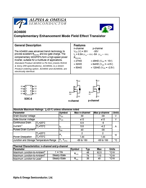
Symbol Typ Max 4862.574110R θJL 3540Steady-State °C/W Thermal Characteristics: n-channel and p-channelMaximum Junction-to-Lead C Steady-State °C/WParameterUnits Maximum Junction-to-AmbientA t ≤ 10s R θJA °C/W Maximum Junction-to-AmbientA AO4600Complementary Enhancement Mode Field Effect TransistorSymbol Min Typ Max Units BV DSS 30V 1T J =55°C 5I GSS100nA V GS(th)0.71 1.4V I D(ON)25A 22.627T J =125°C33402732m Ω4250m Ωg FS1216S V SD0.711V I S 3A C iss 8581050pF C oss 110pF C rss 80pF R g 1.42ΩQ g 9.612nC Q gs 1.65nC Q gd 3nC t D(on) 5.7ns t r 13ns t D(off)37ns t f 4.2ns t rr Body Diode Reverse Recovery time 15.520ns Q rr Body Diode Reverse Recovery charge7.9nC THIS PRODUCT HAS BEEN DESIGNED AND QUALIFIED FOR THE CONSUMER MARKET. APPLICATIONS OR USES AS CRITICALCOMPONENTS IN LIFE SUPPORT DEVICES OR SYSTEMS ARE NOT AUTHORIZED. AOS DOES NOT ASSUME ANY LIABILITY ARISING OUT OF SUCH APPLICATIONS OR USES OF ITS PRODUCTS. AOS RESERVES THE RIGHT TO IMPROVE PRODUCT DESIGN,FUNCTIONS AND RELIABILITY WITHOUT NOTICETurn-Off Fall Time SWITCHING PARAMETERS Total Gate Charge V GS =4.5V, V DS =15V, I D =6.9A Gate Source Charge Gate Drain Charge Turn-On DelayTime V GS =10V, V DS =15V, R L =2.2Ω,R GEN =6ΩReverse Transfer Capacitance Turn-On Rise Time Turn-Off DelayTime Gate resistance V GS =0V, V DS =0V, f=1MHz Forward Transconductance V DS =5V, I D =5A Diode Forward Voltage I S =1A Maximum Body-Diode Continuous Current DYNAMIC PARAMETERS Input Capacitance V GS =0V, V DS =15V, f=1MHzOutput Capacitance R DS(ON)Static Drain-Source On-Resistance V GS =10V, I D =6.9Am ΩV GS =4.5V, I D =6.0AV GS =2.5V, I D =5AGate Threshold Voltage V DS =V GS I D =250µAOn state drain current V GS =4.5V, V DS =5VV DS =24V, V GS =0V µA Gate-Body leakage current V DS =0V, V GS =±12V I F =5A, dI/dt=100A/µsI F =5A, dI/dt=100A/µs n-channel MOSFET Electrical Characteristics (T J =25°C unless otherwise noted)Parameter Conditions STATIC PARAMETERSDrain-Source Breakdown VoltageI D =250µA, V GS =0V I DSSZero Gate Voltage Drain Current A: The value of R θJA is measured with the device mounted on 1in 2 FR-4 board with 2oz. Copper, in a still air environment with T A =25°C. The value in any given application depends on the user's specific board design. The current rating is based on the t ≤ 10s thermal resistance rating.B: Repetitive rating, pulse width limited by junction temperature.C. The R θJA is the sum of the thermal impedence from junction to lead R θJL and lead to ambient.D. The static characteristics in Figures 1 to 6 are obtained using 80 µs pulses, duty cycle 0.5% max.E. These tests are performed with the device mounted on 1 in 2 FR-4 board with 2oz. Copper, in a still air environment with T A =25°C. The SOAcurve provides a single pulse rating.TYPICAL N-CHANNEL ELECTRICAL AND THERMAL CHARACTERISTICSSymbolMin Typ Max Units BV DSS -30V -1T J =55°C -5I GSS±100nA V GS(th)-0.7-1-1.4V I D(ON)-25A 42.549T J =125°C745464m Ω80120m Ωg FS 711S V SD -0.75-1V I S -3A C iss 9521200pF C oss 103pF C rss 77pF R g 5.930ΩQ g 9.512nC Q gs 2nC Q gd 3.1nC t D(on)12ns t r 4ns t D(off)37ns t f 12ns t rr 2126ns Q rr 13nC THIS PRODUCT HAS BEEN DESIGNED AND QUALIFIED FOR THE CONSUMER MARKET. APPLICATIONS OR USES AS CRITICAL COMPONENTS IN LIFE SUPPORT DEVICES OR SYSTEMS ARE NOT AUTHORIZED. AOS DOES NOT ASSUME ANY LIABILITY ARISING OUT OF SUCH APPLICATIONS OR USES OF ITS PRODUCTS. AOS RESERVES THE RIGHT TO IMPROVE PRODUCT DESIGN,FUNCTIONS AND RELIABILITY WITHOUT NOTICE .p-channel MOSFET Electrical Characteristics (T J =25°C unless otherwise noted)Parameter Conditions STATIC PARAMETERSDrain-Source Breakdown VoltageI D =-250µA, V GS =0V I DSSZero Gate Voltage Drain Current V DS =-24V, V GS =0V µA Gate-Body leakage current V DS =0V, V GS =±12V Gate Threshold Voltage V DS =V GS I D =-250µA On state drain current V GS =-4.5V, V DS =-5V R DS(ON)Static Drain-Source On-Resistance V GS =-10V, I D =-5A m ΩV GS =-4.5V, I D =-4A V GS =-2.5V, I D =-1A Forward Transconductance V DS =-5V, I D =-5A Diode Forward Voltage I S =-1A,V GS =0V Maximum Body-Diode Continuous Current DYNAMIC PARAMETERS Input Capacitance V GS =0V, V DS =-15V, f=1MHz Output Capacitance Reverse Transfer Capacitance Gate resistance V GS =0V, V DS =0V, f=1MHz SWITCHING PARAMETERS Total Gate Charge V GS =-4.5V, V DS =-15V, I D =-5A Gate Source Charge Gate Drain Charge Turn-On DelayTime V GS =-10V, V DS =-15V, R L =3Ω, R GEN =6ΩTurn-On Rise Time Turn-Off DelayTime Turn-Off Fall Time Body Diode Reverse Recovery Time I F =-5A, dI/dt=100A/µs Body Diode Reverse Recovery Charge I F =-5A, dI/dt=100A/µsA: The value of R θJA is measured with the device mounted on 1in 2 FR-4 board with 2oz. Copper, in a still air environment with T A =25°C. The value in any a given application depends on the user's specific board design. The current rating is based on the t ≤ 10s thermal resistance rating.B: Repetitive rating, pulse width limited by junction temperature.C. The R θJA is the sum of the thermal impedence from junction to lead R θJL and lead to ambient.D. The static characteristics in Figures 1 to 6,12,14 are obtained using 80 µs pulses, duty cycle 0.5% max.E. These tests are performed with the device mounted on 1 in 2 FR-4 board with 2oz. Copper, in a still air environment with T A =25°C. The SOA curve provides a single pulse rating.A: The value of R θJA is measured with the device mounted on 1in 2 FR-4 board with 2oz. Copper, in a still air environment with T A =25°C. The value in any given application depends on the user's specific board design. The current rating is based on the t ≤ 10s thermal resistance rating.B: Repetitive rating, pulse width limited by junction temperature.C. The R θJA is the sum of the thermal impedence from junction to lead R θJL and lead to ambient.D. The static characteristics in Figures 1 to 6,12,14 are obtained using 80 µs pulses, duty cycle 0.5% max.E. These tests are performed with the device mounted on 1 in 2 FR-4 board with 2oz. Copper, in a still air environment with T A =25°C. The SOA curve provides a single pulse rating.Rev 4 : Sept 2005。
AOS作业指导书(通用型机器)1(2)

通用型机作业指导书
操作图样
※各种接头所缠的圈数一定要准确,注意接头缠的要紧些,防止发生漏水、渗水等现象,同时也要缠平,不要把接头缠到接头所接
与松紧度。
个螺纹牙,※注意接头
低
压
别
高压
(进水)插线
接头方向要垂直向上;同
时注意固定电阀的进出水方向与底座方向,并且要定
30°
出水
20°
快接,螺帽要拧正、拧紧,出水一端水管
操作图样
并与进水电磁阀进水
第二道
4044
第一道出水与第二道进水上水
管连接,同时水管要插到位,并且要把卡子卡上。
操作图样、变压器不需要做头以及卸钉,正负极
黑胶,白生料带不要
外露,接头方向倾斜向上,见图,接
操作图样
个孔要攻丝,注意手枪钻的正确操作
个孔为
(纯水口),注意纯水、废水口
位置
废水位置低)
操作图样箭头
该机器
颗螺
5×16大扁头自攻螺丝注
向别打反。
操作图样4×16元机螺丝
3×10自攻螺丝
3×12自攻螺丝3×8自攻螺丝
螺帽要
)相连
※注意变压器的正负极,线要接紧、接牢;扎注意线的正负极
正极黑色,负极白色)且与各配件插线的正确接法。
操作图样由于瓶盖上的接头都是快接,所以水管要插到位,。
注意纯、废水别上反。
(纯水与高压连接、水与废水比相连接)。
AO3400A 规格书 AOS

ID(A)
15
VDS=5V 12
9
6
125°C 3
25°C
0
0
0.5
1
1.5
2
2.5
3
VGS(Volts) Figure 2: Transfer Characteristics (Note E)
Normalized On-Resistance
RDS(ON) (mΩ)
30
25 VGS=4.5V
20
15
S
Absolute Maximum Ratings TA=25°C unless otherwise noted
Parameter
Symbol
Drain-Source Voltage
VDS
Gate-Source Voltage
VGS
Continuous Drain Current
TA=25°C TA=70°C
Crss
Reverse Transfer Capacitance
Rg
Gate resistance
VGS=0V, VDS=15V, f=1MHz VGS=0V, VDS=0V, f=1MHz
630
pF
75
pF
50
pF
1.5
3
4.5
Ω
SWITCHING PARAMETERS
Qg
Total Gate Charge
B. The power dissipation PD is based on TJ(MAX)=150°C, using ≤ 10s junction-to-ambient thermal resistance. C. Repetitive rating, pulse width limited by junction temperature TJ(MAX)=150°C. Ratings are based on low frequency and duty cycles to keep initialTJ=25°C. D. The RθJA is the sum of the thermal impedence from junction to lead RθJL and lead to ambient. E. The static characteristics in Figures 1 to 6 are obtained using <300µs pulses, duty cycle 0.5% max. F. These curves are based on the junction-to-ambient thermal impedence which is measured with the device mounted on 1in2 FR-4 board with
Nailor Industries A3400和A34RW E5型号分压器说明说明书

DAMPER 100
OPEN 80
PROP. BAND
DIAL SET POINT CENTERED IN DEAD BAND 2°F (1.1°C)
PROP. BAND
DAMPER OPEN
HEATING PERIMETER OR HOT WATER REHEAT
Cooling Mode:
Supply air system in cooling mode (below 75°F (24°C)). On a rise in room temperature above set point, the bypass damper will modulate open, increasing the flow of cool air to the room, closing the bypass at the same time. On a fall in room temperature below set point, the bypass damper will modulate closed, reducing the flow of cool air into the room and opening the bypass at the same time. If room temperature continues to fall, the thermostat will energize the control relay/valve of the auxiliary perimeter heating (electric or hot water) or hot water terminal unit hot water coil valve for reheat.
AO3400 SOT-23-3L NMOS Vds30V 规格书AO推荐

ID(A)
15
VDS=5V 12
9
6
125°C 3
25°C
0
0
0.5
1
1.5
2
2.5
3
VGS(Volts) Figure 2: Transfer Characteristics (Note E)
Normalized On-Resistance
RDS(ON) (mΩ)
30
25 VGS=4.5V
20
15
Symbol
Parameter
Conditions
Min Typ Max Units
STATIC PARAMETERS
BVDSS Drain-Source Breakdown Voltage
ID=250µA, VGS=0V
30
V
IDSS
Zero Gate Voltage Drain Current
VDS=30V, VGS=0V
Parameter
Symbol
Drain-Source Voltage
VDS
Gate-Source Voltage
VGS
Continuous Drain Current
TA=25°C TA=70°C
ID
Pulsed Drain Current C
IDM
TA=25°C Power Dissipation B TA=70°C
(Note E)
IS (A)
1.0E+01
1.0E+00
40
1.0E-01
1.0E-02
1.0E-03
125°C
25°C
1.0E-04
1.0E-05
ao3400中文资料

O3400a数据手册规格AO3401A中文信息PDF)MOS晶体管-MOS管测试步骤:5:MOS晶体管的Gate AOS公司MOS管7407导线的连接使栅极电荷释放,内部电场消失,导电沟道消失,因此漏极和源极之间的电阻变得无限大。
此时,用一根导线连接被测管的栅极和源,万用表的指针将立即返回无穷大,如图5-6所示。
6:MOS晶体管源AOS半导体MOS晶体管74117:VDMOS,MOSFET,osmos晶体管MOS 7413(ao3400a数据手册规格AO3401A中文信息PDF)MOS晶体管8:MESFET如何工作AOS模拟开关MOS 74159:双栅极MOSFET AOSTVS二极管MOS晶体管7417如果去除了电阻,则探针将逐渐恢复为高电阻甚至无限大,因此应考虑被测管的栅极泄漏。
此时处于图5-4的状态;然后将连接的电阻移开,然后万用表的指针仍应为MOS晶体管导通指数保持不变,如图5-5所示。
尽管去除了电阻,但是由于由电阻充电至栅极的电荷不会消失,因此栅极电场继续保持,内部导电沟道保持不变,这是绝缘栅MOS晶体管的特性。
10:功率MOSFET有源模块MOS管740111:电子零件MOS管7405(ao3400a数据手册规格AO3401A中文信息PDF)MOS晶体管12:AOS公司的MOS FET参数MOS 780013:用于MOS FET的AOS半导体MOS晶体管7801此时,使用100k-200k电阻连接栅极和漏极,如图5-4所示。
此时,欧姆越小越好。
通常,它可以指示0欧姆。
此时,正电荷通过100k电阻为高功率MOS晶体管的栅极充电,以产生栅极电场。
随着电场的产生,导电通道导致漏极和源极连接,因此万用表指针会偏转并偏转角度。
高度(小欧姆指数)表示良好的放电性能。
14:MOSFET AOS代理MOS晶体管340015:什么是场效应管MOS晶体管3400a(ao3400a数据手册规格AO3401A中文信息PDF)MOS晶体管16:什么是MOS晶体管MOS晶体管340217:MOSFET的基础知识MOS晶体管3404将红色探针连接到MOS晶体管的源极,将黑色探针连接到MOS晶体管的漏极D。
AO3409 规格书AOS

Symbolt ≤ 10s Steady-State Steady-StateR θJLMaximum Junction-to-Ambient A Maximum Junction-to-Lead°C/W°C/W Maximum Junction-to-Ambient A D 6312580°C/W R θJA V W AV Units 7010090°CThermal Characteristics Units ParameterTyp MaxSymbolMin Typ Max Units BV DSS -30VV DS =-30V, V GS =0V-1T J =55°C -5I GSS ±100nA V GS(th)Gate Threshold Voltage -1.4-1.9-2.4V I D(ON)-20A 77110T J =125°C100140125180m Ωg FS 5S V SD -0.8-1V I S-1.5A C iss 197240pF C oss 42pF C rss 2637pF R g3.57.211.0ΩQ g (10V) 4.35.2nC Q g (4.5V) 2.23nC Q gs 0.7nC Q gd 1.1nC t D(on)7.5ns t r 4.1ns t D(off)11.8ns t f 3.8nst rr 11.314ns Q rr4.4nCTHIS PRODUCT HAS BEEN DESIGNED AND QUALIFIED FOR THE CONSUMER MARKET. APPLICATIONS OR USES AS CRITICAL COMPONENTS IN LIFE SUPPORT DEVICES OR SYSTEMS ARE NOT AUTHORIZED. AOS DOES NOT ASSUME ANY LIABILITY ARISING OUT OF SUCH APPLICATIONS OR USES OF ITS PRODUCTS. AOS RESERVES THE RIGHT TO IMPROVE PRODUCT DESIGN,FUNCTIONS AND RELIABILITY WITHOUT NOTICE.R DS(ON)Static Drain-Source On-ResistanceDiode Forward VoltageI F =-2.6A, dI/dt=100A/µsV GS =0V, V DS =-15V, f=1MHz SWITCHING PARAMETERSBody Diode Reverse Recovery TimeI DSS µA Drain-Source Breakdown Voltage On state drain currentI D =-250µA, V GS =0V V GS =-10V, V DS =-5V V DS =0V, V GS = ±20V Zero Gate Voltage Drain Current Gate-Body leakage current V DS =V GS I D =-250µA Electrical Characteristics (T J =25°C unless otherwise noted)STATIC PARAMETERS ParameterConditions m ΩForward Transconductance Gate resistanceV GS =0V, V DS =0V, f=1MHzV GS =-10V, I D =-2.6AReverse Transfer Capacitance I S =-1A,V GS =0VV DS =-5V, I D =-2.6A V GS =-4.5V, I D =-2AMaximum Body-Diode Continuous CurrentInput Capacitance Output CapacitanceTurn-On DelayTime DYNAMIC PARAMETERSTotal Gate Charge V GS =-10V, V DS =-15V, I D =-2.6AGate Source Charge Gate Drain Charge V GS =-10V, V DS =-15V, R L =5.8Ω,R GEN =3ΩTotal Gate Charge Body Diode Reverse Recovery Charge I F =-2.6A, dI/dt=100A/µsTurn-On Rise Time Turn-Off DelayTime Turn-Off Fall TimeA. The value of R θJA is measured with the device mounted on 1in 2FR-4 board with 2oz. Copper, in a still air environment with T A =25°C. The value in any given application depends on the user's specific board design.B. The power dissipation P D is based on T J(MAX)=150°C, using ≤ 10s junction-to-ambient thermal resistance.C. Repetitive rating, pulse width limited by junction temperature T J(MAX)=150°C. Ratings are based on low frequency and duty cycles to keep initialT J =25°C.D. The R θJA is the sum of the thermal impedence from junction to lead R θJL and lead to ambient.E. The static characteristics in Figures 1 to 6 are obtained using <300µs pulses, duty cycle 0.5% max.F. These curves are based on the junction-to-ambient thermal impedence which is measured with the device mounted on 1in 2 FR-4 board with2oz. Copper, assuming a maximum junction temperature of T J(MAX)=150°C. The SOA curve provides a single pulse ratin g.TYPICAL ELECTRICAL AND THERMAL CHARACTERISTICS-V GS (Volts)Figure 2: Transfer Characteristics (Note E)-I D (A )-V DS (Volts)Fig 1: On-Region Characteristics (Note E)-I D (A )TYPICAL ELECTRICAL AND THERMAL CHARACTERISTICS12345Q g (nC)Figure 7: Gate-Charge Characteristics-V G S (V o l t s )51015202530-V DS (Volts)Figure 8: Capacitance Characteristics C a p a c i t a n c e (p F )VdsChargeGate Charge Test Circuit & WaveformVddVdsIdVgsUnclamped Inductive Switching (UIS) Test Circuit & Waveforms2E = 1/2 LI AR ARBV DSSI ARVdd VddResistive Switching Test Circuit & Waveforms90%10%。
ao3400中文资料

ao3400中文资料场效应管(Field Effect Transistor,缩写FET)是场效应晶体管的简称,是利用控制输入回路的电场效应来控制输出回路电流的一种半导体器件。
它主要有两种类型:结型场效应管和金属- 氧化物半导体场效应管,具有输入电阻高(107~1015Ω)、噪声小、功耗低、动态范围大、易于集成、没有二次击穿现象等优点。
与双极型晶体管相比,场效应管具有如下特点。
(1)场效应管是电压控制器件,它通过VGS(栅源电压)来控制ID(漏极电流);(2)场效应管的控制输入端电流极小,因此它的输入电阻(107~1012Ω)很大。
(3)它是利用多数载流子导电,因此它的温度稳定性较好;(4)它组成的放大电路的电压放大系数要小于三极管组成放大电路的电压放大系数;(5)场效应管的抗辐射能力强;(6)由于它不存在杂乱运动的电子扩散引起的散粒噪声,所以噪声低。
场效应管工作原理用一句话说,就是“漏极-源极间流经沟道的ID,用以栅极与沟道间的pn结形成的反偏的栅极电压控制ID”。
更正确地说,ID流经通路的宽度,即沟道截面积,它是由pn结反偏的变化,产生耗尽层扩展变化控制的缘故。
在VGS=0的非饱和区域,表示的过渡层的扩展因为不很大,根据漏极-源极间所加VDS的电场,源极区域的某些电子被漏极拉去,即从漏极向源极有电流ID流动。
从门极向漏极扩展的过度层将沟道的一部分构成堵塞型,ID饱和。
将这种状态称为夹断。
这意味着过渡层将沟道的一部分阻挡,并不是电流被切断。
在过渡层由于没有电子、空穴的自由移动,在理想状态下几乎具有绝缘特性,通常电流也难流动。
但是此时漏极-源极间的电场,实际上是两个过渡层接触漏极与门极下部附近,由于漂移电场拉去的高速电子通过过渡层。
因漂移电场的强度几乎不变产生ID的饱和现象。
其次,VGS向负的方向变化,让VGS=VGS(off),此时过渡层大致成为覆盖全区域的状态。
而且VDS的电场大部分加到过渡层上,将电子拉向漂移方向的电场,只有靠近源极的很短部分,这更使电流不能流通。
AO3400AC开关MOS管
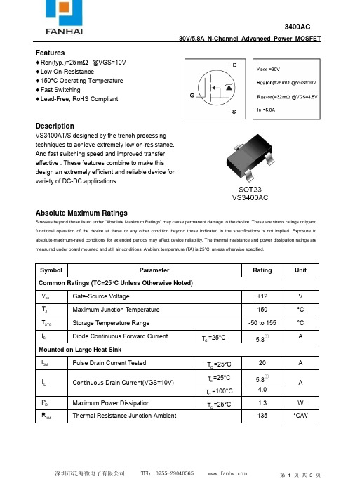
Mounted on Large Heat Sink
TC =25°C
IDM
Pulse Drain Current Tested
ID
Continuous Drain Current(VGS=10V)
PD
Maximum Power Dissipation
Rθ JA
Thermal Resistance Junction-Ambient
Coss
Output Capacitance
Crss
Reverse Transfer Capacitance
Qg
Total Gate Charge
Q gs
Gate-Source Charge
Q gd
Gate-Drain Charge
Switching Characteristics
VDS=15V,VGS=0V, f=1MHz
Pulsed Source-drain current (Body Diode)
Tc=25℃
VSD
Forward on voltage
Tj=25℃,ISD=2.8A, VGS=0V
Notes: ① Pulse test ; Pulse width≤300μs, duty cycle≤2%.
--
--
①
VDS=15V,ID=5.8A, VGS=4.5V
--
330
-- pF
--
105
-- pF
--
30
-- pF
--
11
-- nC
--
1.6
-- nC
--
2.7
-- nC
t d(on)
Turn-on Delay Time
ao3400中文资料

ao3400中文资料半导体(Semiconductor)是一种电导率在绝缘体至导体之间的物质,其电导率容易受控制,可作为信息处理的元件材料。
从科技或是经济发展的角度来看,半导体非常重要。
很多电子产品,如计算机、移动电话、数字录音机的核心单元都是利用半导体的电导率变化来处理信息。
常见的半导体材料有硅、锗、砷化镓等,而硅更是各种半导体材料中,在商业应用上最具有影响力的一种。
顾名思义:常温下导电性能介于导体(conductor)与绝缘体(insulator)之间的材料,叫做半导体(semiconductor)。
物质存在的形式多种多样,固体、液体、气体、等离子体等等。
我们通常把导电性和导电导热性差或不好的材料,如金刚石、人工晶体、琥珀、陶瓷等等,称为绝缘体。
而把导电、导热都比较好的金属如金、银、铜、铁、锡、铝等称为导体。
可以简单的把介于导体和绝缘体之间的材料称为半导体。
与导体和绝缘体相比,半导体材料的发现是最晚的,直到20世纪30年代,当材料的提纯技术改进以后,半导体的存在才真正被学术界认可。
半导体的分类,按照其制造技术可以分为:集成电路器件,分立器件、光电半导体、逻辑IC、模拟IC、储存器等大类,一般来说这些还会被分成小类。
此外还有以应用领域、设计方法等进行分类,虽然不常用,单还是按照IC、LSI、VLSI(超大LSI)及其规模进行分类的方法。
此外,还有按照其所处理的信号,可以分成模拟、数字、模拟数字混成及功能进行分类的方法。
基本定义电阻率介于金属和绝缘体之间并有负的电阻温度系数的物质。
半导体室温时电阻率约在10E-5~10E7欧·米之间,温度升高时电阻率指数则减小。
半导体材料很多,按化学成分可分为元素半导体和化合物半导体两大类。
锗和硅是最常用的元素半导体;化合物半导体包括Ⅲ-Ⅴ 族化合物(砷化镓、磷化镓等)、Ⅱ-Ⅵ族化合物( 硫化镉、硫化锌等)、氧化物(锰、铬、铁、铜的氧化物),以及由Ⅲ-Ⅴ族化合物和Ⅱ-Ⅵ族化合物组成的固溶体(镓铝砷、镓砷磷等)。
Alpha锡膏OM340EN规格书英文版

Alpha锡膏OM340EN规格书英文版FINE __, ZERO __1, LOW HEAD IN PILLOW DEFECT, HIGHLY PIN __E__TION__-340 - NO-CLEAN, LEAD-FREE SOLDER PASTEALPHA OM-340 is a lead-free, no-clean solder paste designed for a broad range of applications. ALPHA OM-340 provides best in class low defect rate for Head in Pillow defects combined with excellent first pass yield on ICT/pin testing. ALPHA OM-340 also yields excellent print capability performance across various board designs and, particularly, with ultra fine feature repeatability and high “through-put” applications.Outstanding reflow process window delivers superior soldering on CuOSP with excellent coalescence on a broad range of deposit sizes, excellent random solder ball resistance and mid-chip solder ball performance. ALPHA OM-340 is formulated to deliver excellent visual joint cosmetics and best in class in circuit pin test yields. Additionally, ALPHA OM-340’s capability of IPC Class III for voiding and ROL0 IPC classifications ensures maximum long-term product reliability.1Zero halogen is defined as no halogen is intentionally added to the formulation__S __SMaximizes reflow yield for lead-free processing, allowing full alloy coalescence at circular dimensions as small as 200μm (8 mil) with 100μm (4 mil) thick stencilsExcellent print consistency with high process capability index across all board designs.Print sp eeds of up to 150mm/sec (6”/sec), enabling a fast print cycle time and a high throughput. Wide reflow profile window with good solderability on various board / component finishes. Excellent solder and flux cosmetics after reflow soldering Best in class low defect rate for Head in Pillow Best in class in circuit pin test yieldReduction in random solderballing levels, minimizing rework and increasing first time yield Meets highest IPC 7095 voiding performance classification of Class III Excellent reliability properties, halide-free material Compatible with either nitrogen or air reflowZero halogen (No halogen intentionally added to theformulation)__ __TIONSAC305 (96.5%Sn/3.0%Ag/0.5%Cu) SAC405 (95.5%Sn/4.0%Ag/0.5%Cu)SACX Plus 0307 (99%Sn/0.3%Ag/0.7%Cu) SACX Plus 0807 (98.5%Sn/0.8%Ag/0.7%Cu)InnoLot (90.95%Sn/3.8%Ag/0.7%Cu/1.4%Sb/0.15%Ni/3%Bi)For other alloys, please contact your local Cookson Electronics Sales Office. Type 3 (25 - 45μm per IPC J-STD-005) Type 4 (20 - 38μm per IPC J-STD-005)Type 4.5 (Proprietary Powder Size Distribution) C available upon request Type 5 (15 - 25μm per IPC J-STD-005) C available upon request Approximately 5% by (w/w) Complies with RoHS Directive 2022年/95/EC.__TIONFormulated for both standard and fine pitch stencil printing, at print speeds of between 25mm/sec (1”/sec) and 150mm/sec (6”/sec), with stencil thickness of 100μm (4 mil) to 150μm (6 mil), particularly when used with ALPHA Stencils. Blade pressures should be 0.18-0.27 kg/cm of blade (1.0 -1.5 Ibs/inch), depending upon the print speed. The higher the print speedemployed, the higher the blade pressure that is required. The reflow process window will give high soldering yield with good cosmetics and minimized rework.__ STATUSALPHA OM-340 is a Zero Halogen product and passes the standards listed in the Table below:Halogen StandardsStandardJEITA ET-7304Definition of Halogen Free Soldering Materials IEC __-2-21 JEDECA Guideline for Definin g “Low Halogen" ElectronicsRequirement1000 ppm Br, Cl, F in solder material solids Post Soldering Residues contain900 ppm each or total of 1500 ppm Br or Cl from flame retardant sourcePost soldering residues contain1000 ppm Br or Cl from flame retardant sourceTest Method StatusPassTM EN __PassPassZero Halogen: No halogenated compounds have been intentionally added to this productSAFETYWhile the ALPHA OM-340 flux system is not considered toxic, its use in typical reflow will generate a small amount of reaction and decomposition vapors. These vapors should be adequately exhausted from the work area. Consult the most recent MSDS (available at ) for additional safety information.____RES/__ALPHA OM-340 Technical Data__Y__L __IESActivity Level Halide Content Halogen Content Copper MirrorCopper Corrosion Test____CAL __IES SIR(IPC 7 days @ 85° C/85% RH) SIR(Bellcore 96 hours @ 35°C/85%RH) Electro migrationROL0 IPC J-STD-004 Halide free (by titration). Passes Ag IPC J-STD-004 Chromate TestPass, Zero Halogen - No halogen EN__, by oxygen bomb combustion, intentionally added Non-detectable (ND) at 50 ppm Pass IPC J-STD-004PassPass, 8.6 x 10⁹ ohms Pass, 2.1 x 10¹¹ ohms Pass, Initial = 3.9 x 10 ohmsClear, Colorless Flux Residue(Bellcore 96 hours @ 65°C/85%RH 10V 500 hours)__L __IES (Using 88.0% Metal, IPC Type 3 Powder, unless otherwise noted) ColorTack Force vs. Humidity(t=8 hours)Final = 1.9 x 10⁹ ohmsIPC J-STD-0048(Pass ≥ 1 x 10ohm) Bellcore GR78-CORE11(Pass ≥ 1 x 10 ohm) Bellcore GR78-CORE (Pass=final initial/10)Pass, Change of 1 g/mm2 over 24 hoursat 25% and 75 % Relative HumidityIPC J-STD-005 TM-650 2.4.44 JIS Z3284 Annex 9Pass, Change of 10% when stored at25±2C and 50±10% relative humidity. Type 3 powder, 88.0% metal load designated M16 for printingViscosity (Typical) 1600 poise at 10 RPM MalcomType 4 powder, 88.3% metal load designated M18 for printingViscosity (Typical) 1800 poise at 10 RPM MalcomType 4 powder, 84% metal load, designated M06 for dispensingType 4 powder, 85% metal load, designated M08 for dispensingType 5 powder, 88.3% metal load designated M19 for printingType 5 powder, 78% metal load, designated M04 for dispensingType 6 powder, 78% metal load, designated M04 for dispensingoViscosity Malcom Spiral Viscometer; J-STD-005Solderball Stencil Life SpreadAcceptable (SAC 305 and SAC405 alloys) Pass, Class I - 1 hour and 72 hour8 hoursIPC J-STD-005DIN Standard 32 513, 4.4@ 50%RH, 25C (74°F) JIS-Z-3197: 1999 8.3.1.1 IPC J-STD-005 (10 min 150C) TM-650 2.4.35JIS-Z-3284-1994 Annex 7oPass PassSlumpNo bridging 0.2 mm gap above No bridging 0.3 mm gap aboveJIS-Z-3284-1994 Annex 8ALPHA OM-340 Processing Guidelines__ and __GRefrigerate to guarantee stability @ 0-10°C (32-50°F)__GRecommend CooksonElectronics ALPHA CUT ,ALPHA NICKEL-CUT , ALPHA__ND , or __RM stencils @ 0.100mm - 0.150 mm (4-6 mil) thick for 0.4 - 0.5 mm (0.016” or 0.020”) pitch. Stencil design is subject to many process variables. Contact your local Cookson Electronics stencil site for advice.Metal (recommended)PASTE ROLL: 1.5-2.0 cmdiameter and make additions when roll reaches 1-cm (0.4”) diameter (min). Max roll size will depend upon blade__E: 0.45 to 0.7 kg/inch 25 to 150mm per second (1 to 6 inches per second). : 3-10mm/sec.PRINT PUMP HEAD: Passes DEK ProFlow compatibility test REFLOW (See Figure 1)Clean-dry air or nitrogen atmosphere.Acceptable reflow / coalescence for feature size down to 8 mil (200 μm). IPC Class IIIvoiding obtained for both straight ramp and soak profiles.__GALPHA OM-340 residue isdesigned to remain on the board after reflow.If reflowed residue cleaning is required, the following aqueous cleaners are recommended: In-line or Batch Cleaners - ALPHA BC-2200 - Zestron Vigon A201 - Zestron Vigon A250 - Zestron Vigon USManual or solvent cleaning: - ALPHA SM-110 and SM-110E - BioactTM SC-10 and SC-10EMisprints and stencil cleaning may be done with the following cleaners:ALPHA SM-110E ALPHA SM-440Zestron Vigon SC200TMBioact SC-10EShelf life of refrigerated paste is 6 months.Paste can be stored for 2 weeks at roomotemperatures up to 25C (77°F) prior to use.When refrigerated, warm-up of paste container to room temperature for up to 4 hours. Paste must beoo≥19C (66F) before processing. Verify pastetemperature with a thermometer to ensure paste isooat 19C (66F) or greater before setup. Printing canoobe performed at temperatures up to 32C (89F).Paste can be manually stirred before use. A rotating, centrifugal force mixing operation is not required. If a rotating/centrifugal force mixing is used, 30 - 60 seconds at 300 RPM is adequate.Do not remove worked paste from stencil and mix with unused paste in jar. This will alter rheology of unused paste.These are starting recommendations and allprocess settings should be reviewed independently.Note 1: Refer to component and board supplier data for thermal properties at elevated temperatures. Lower peak temperatures require longer TAL for improved joint cosmetics. Keeping the peaktemperature below 240°C will lower the amount of voiding.Figure 1: ALPHA OM-340 SAC305 Typical Reflow ProfileParameter Atmosphere SAC305, SAC405, SACX Plus 0807 SACX Plus 0307 Setting Zone* o 40°C to 225 C 170°C to 225°C 120°C to 225°C TAL (217 - 225°C) Peak temperatureALPHA OM-340 - General Reflow Profile Guidelines Guideline Additional Information Air or N2 217 - 225°C Melting Range 217 - 227°C Melting Range Optimal Dwell Period Extended window 2:30 to 4:30 min. 5:00 min. 0:30 to 2:00 min 2:30 min. 1:25 to 3:00 min. 3:30 min. 45 - 90 sec. Not Recommended Compatible with most common surface finishes. (Entek HT, Entek OM, Alpha Star, ENIG, SACX 235 - 245°C HASL) 1 - 6°C/second Recommended to prevent surface cracking issues.Joint cool down rate from 170°C* Above recommendations are for SAC305. For alternative alloys, please follow the liquidus temperature of the respective alloy.109 Corporate Blvd., South Plainfield, NJ 07080, 1-800-367-5460,。
AO3400_datasheet
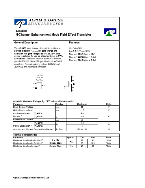
SymbolTyp Max 659085125R θJL 4360Maximum Junction-to-LeadCSteady-State°C/WThermal Characteristics ParameterUnits Maximum Junction-to-AmbientAt ≤ 10s R θJA °C/W Maximum Junction-to-AmbientASteady-State °C/W AO3400SymbolMin TypMaxUnits BV DSS 30V 1T J =55°C5I GSS 100nA V GS(th)0.7 1.11.4V I D(ON)30A 22.828T J =125°C323927.333m Ω43.352m Ωg FS 1015S V SD 0.711V I S2.5A C iss 8231030pF C oss 99pF C rss 77pF R g1.2 3.6ΩQ g 9.712nC Q gs 1.6nC Q gd 3.1nC t D(on) 3.35ns t r 4.87ns t D(off)26.340ns t f 4.16ns t rr 1620ns Q rr8.912nCTHIS PRODUCT HAS BEEN DESIGNED AND QUALIFIED FOR THE CONSUMER MARKET. APPLICATIONS OR USES AS CRITICAL COMPONENTS IN LIFE SUPPORT DEVICES OR SYSTEMS ARE NOT AUTHORIZED. AOS DOES NOT ASSUME ANY LIABILITY ARISING OUT OF SUCH APPLICATIONS OR USES OF ITS PRODUCTS. AOS RESERVES THE RIGHT TO IMPROVE PRODUCT DESIGN,FUNCTIONS AND RELIABILITY WITHOUT NOTICE.Gate resistanceV GS =0V, V DS =0V, f=1MHzTurn-Off Fall TimeMaximum Body-Diode Continuous CurrentInput Capacitance Output Capacitance Turn-On DelayTime DYNAMIC PARAMETERS I F =5A, dI/dt=100A/µsV GS =0V, V DS =15V, f=1MHz SWITCHING PARAMETERS Total Gate Charge V GS =4.5V, V DS =15V, I D =5.8AGate Source Charge Gate Drain Charge Turn-On Rise Time Turn-Off DelayTime V GS =10V, V DS =15V, R L =2.7Ω, R GEN =3Ωm ΩV GS =4.5V, I D =5A I S =1A,V GS =0V V DS =5V, I D =5AR DS(ON)Static Drain-Source On-ResistanceForward TransconductanceDiode Forward VoltageI DSS µA Gate Threshold Voltage V DS =V GS I D =250µA V DS =24V, V GS =0VV DS =0V, V GS =±12V Zero Gate Voltage Drain Current Gate-Body leakage current Electrical Characteristics (T J =25°C unless otherwise noted)STATIC PARAMETERS ParameterConditions Body Diode Reverse Recovery TimeBody Diode Reverse Recovery Charge I F =5A, dI/dt=100A/µsDrain-Source Breakdown Voltage On state drain currentI D =250µA, V GS =0V V GS =2.5V, I D =4AV GS =4.5V, V DS =5V V GS =10V, I D =5.8AReverse Transfer Capacitance A: The value of R θJA is measured with the device mounted on 1in 2 FR-4 board with 2oz. Copper, in a still air environment with T A =25°C. The value in any given application depends on the user's specific board design. The current rating is based on the t ≤ 10s thermal resistance rating.B: Repetitive rating, pulse width limited by junction temperature.C. The R θJA is the sum of the thermal impedence from junction to lead R θJL and lead to ambient.D. The static characteristics in Figures 1 to 6,12,14 are obtained using 80 µs pulses, duty cycle 0.5% max.E. These tests are performed with the device mounted on 1 in 2FR-4 board with 2oz. Copper, in a still air environment with T A =25°C. The SOA curve provides a single pulse rating. Rev 4 : June 2005。
AO3403 规格书 AOS
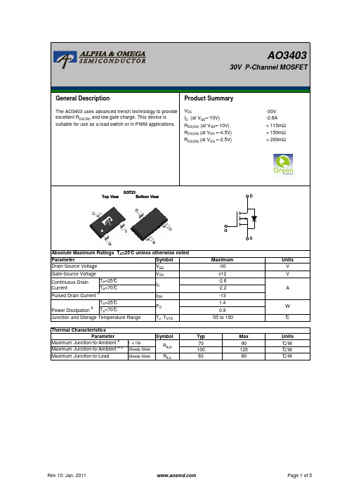
RDS(ON) (mΩ)
250
200
150
100
25°C
ID=-2.6A 125°C
50
0
2
4
6
8
10
-VGS (Volts) Figure 5: On-Resistance vs. Gate-Source Voltage
(Note E)
-IS (A)
1.0E+02
1.0E+01
40
VDS ID (at VGS=-10V) RDS(ON) (at VGS=-10V) RDS(ON) (at VGS =-4.5V) RDS(ON) (at VGS =-2.5V)
-30V -2.6A < 115mΩ < 150mΩ < 200mΩ
SOT23
Top View
Bottom View
D
D D
S
G
G
S
Absolute Maximum Ratings TA=25°C unless otherwise noted
Parameter
Symbol
Drain-Source Voltage
VDS
Gate-Source Voltage
VGS
Continuous Drain Current
TA=25°C TA=70°C
RDS(ON) (mΩ)
210
190
VGS=-2.5V
170
150
130
VGS=-4.5V
110
90
70
VGS=-10V
50
0
1
2
3
4
5
AO3404 规格书 AOS
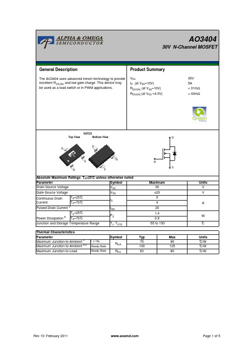
Power (W)
10000 1000
TA=25°C
100
10
1
0.00001 0.001
0.1
10
1000
Pulse Width (s) Figure 11: Single Pulse Power Rating Junction-to-
Ambient (Note F)
In descending order D=0.5, 0.3, 0.1, 0.05, 0.02, 0.01, single pulse
Ciss
Input Capacitance
Coss
Output Capacitance
Crss
Reverse Transfer Capacitance
Rg
Gate resistance
VGS=0V, VDS=15V, f=1MHz VGS=0V, VDS=0V, f=1MHz
255 310 pF
45
AO3404
30V N-Channel MOSFET
General Description
Product Summary
The AO3404 uses advanced trench technology to provide excellent RDS(ON) and low gate charge. This device may be used as a load switch or in PWM applications.
ID=-250µA, VGS=0V
30
IDSS
Zero Gate Voltage Drain Current
VDS=30V, VGS=0V
TJ=55°C
AO3401MOS场效应管规格书
AO3401MOS场效应管规格书AO3401 是一种常用的 MOS 场效应管,在电子电路设计中有着广泛的应用。
以下将为您详细介绍 AO3401 MOS 场效应管的各项规格参数。
一、基本特性1、极性AO3401 为增强型 P 沟道 MOS 场效应管。
2、封装形式常见的封装形式有 SOT-23 等,这种小型封装使其在电路板上占用空间较小,有利于电路的小型化设计。
二、电气参数1、漏源极击穿电压(V(BR)DSS)AO3401 的漏源极击穿电压通常为-30V,这意味着在正常工作条件下,漏源极之间能够承受的最大电压为-30V,超过这个电压可能会导致器件损坏。
2、栅源极击穿电压(V(BR)GSS)其栅源极击穿电压一般为 ±20V,在操作时应注意避免超过此电压限制。
3、漏极连续电流(ID)在环境温度为 25℃时,AO3401 的漏极连续电流可达-42A,这表明它能够持续通过的最大电流为-42A。
4、栅极阈值电压(VGS(th))栅极阈值电压典型值约为-15V 到-25V 之间。
5、导通电阻(RDS(on))导通电阻是衡量 MOS 管性能的一个重要参数。
AO3401 在 VGS =-45V 时,导通电阻典型值约为70mΩ;在 VGS =-10V 时,导通电阻典型值约为38mΩ。
较小的导通电阻有助于降低电路的功率损耗,提高效率。
三、动态特性1、输入电容(Ciss)AO3401 的输入电容通常在几十到几百皮法之间,具体数值会因测试条件和批次而有所差异。
2、输出电容(Coss)输出电容的大小也会影响器件的开关速度和频率特性。
3、反向传输电容(Crss)反向传输电容对电路的稳定性和高频性能有一定的影响。
四、温度特性1、工作温度范围AO3401 能够在-55℃到+150℃的温度范围内正常工作,具有较好的温度适应性。
2、温度系数一些电气参数,如导通电阻和阈值电压等,会随着温度的变化而有一定的漂移,在设计电路时需要考虑这些温度系数的影响。
AO3401MOS场效应管规格书

AO3401MOS场效应管规格书一、AO3401 MOS 场效应管概述AO3401 是一款常见的增强型 MOS 场效应管,在电子电路中有着广泛的应用。
它具有低导通电阻、高开关速度和低栅极电荷等特性,适用于多种电源管理、开关电路和信号放大等领域。
二、AO3401 MOS 场效应管的主要参数1、漏极源极电压(VDS)AO3401 的漏极源极电压额定值通常为 30V,这意味着在正常工作条件下,漏极和源极之间所能承受的最大电压为 30V。
超过此电压可能会导致器件损坏。
2、栅极源极电压(VGS)其栅极源极电压的额定值一般为 ±12V。
在实际应用中,需要确保施加在栅极和源极之间的电压在这个范围内,以保证管子的正常工作和可靠性。
3、连续漏极电流(ID)AO3401 在 25℃环境温度下,连续漏极电流通常能够达到 42A。
但需要注意的是,实际工作中的电流承载能力还会受到散热条件、工作温度等因素的影响。
4、导通电阻(RDS(on))导通电阻是 MOS 管的一个重要参数,AO3401 在 VGS = 45V 时,导通电阻典型值约为70mΩ;在 VGS = 10V 时,导通电阻典型值约为38mΩ。
较低的导通电阻有助于降低功率损耗,提高电路效率。
5、输入电容(Ciss)输入电容的值约为 130pF,它会影响管子的开关速度和驱动电路的设计。
6、输出电容(Coss)输出电容大约为 55pF,对电路的高频特性有一定的影响。
7、反向传输电容(Crss)反向传输电容约为 18pF,在高频应用中需要考虑其对电路性能的影响。
8、封装形式AO3401 常见的封装形式有 SOT-23、SOT-89 等,不同的封装形式在散热性能、安装方式和占用空间等方面有所不同,用户可以根据实际需求进行选择。
三、AO3401 MOS 场效应管的工作原理MOS 场效应管的工作原理基于电场对导电沟道的控制。
对于AO3401 这种增强型 MOS 管,当栅极源极电压低于阈值电压(Vth)时,漏极和源极之间几乎没有电流通过,处于截止状态。
- 1、下载文档前请自行甄别文档内容的完整性,平台不提供额外的编辑、内容补充、找答案等附加服务。
- 2、"仅部分预览"的文档,不可在线预览部分如存在完整性等问题,可反馈申请退款(可完整预览的文档不适用该条件!)。
- 3、如文档侵犯您的权益,请联系客服反馈,我们会尽快为您处理(人工客服工作时间:9:00-18:30)。
VGS=10V
1.8
VGS=4.5V Id=5A 1.6
1.4
17
VGS=105V
1.2
Id=5.8A2
10
1
10
0
5
10
15
20
ID (A)
Figure 3: On-Resistance vs. Drain Current and Gate
Voltage (Note E)
0.8 0
25 50 75 100 125 150 175
In descending order D=0.5, 0.3, 0.1, 0.05, 0.02, 0.01, single pulse
ZθJA Normalized Transient Thermal Resistance
ID(A)
15
VDS=5V 12
9
6
125°C 3
25°C
0
0
0.5
1
1.5
2
2.5
3
VGS(Volts) Figure 2: Transfer Characteristics (Note E)
Normalized On-Resistance
RDS(ON) (mΩ)
30
25 VGS=4.5V
20
15
AO3400
30V N-Channel MOSFET
General Description
Product Summary
The AO3400 combines advanced trench MOSFET technology with a low resistance package to provide extremely low RDS(ON). This device is suitable for use as a load switch or in PWM applications.
TJ=55°C
1 µA
5
IGSS
Gate-Body leakage current
VDS=0V, VGS= ±12V
100 nA
VGS(th) Gate Threshold Voltage
VDS=VGS ID=250µA
0.65 1.05 1.45 V
ID(ON)
On state drain current
TA=25°C
10
1
0.00001 0.001
0.1
10
1000
Pulse Width (s) Figure 10: Single Pulse Power Rating Junction-to-
Ambient (Note F)
10 D=Ton/T TJ,PK=TA+PDM.ZθJA.RθJA
1 RθJA=125°C/W
VGS=4.5V, VDS=5V
30
A
RDS(ON) Static Drain-Source On-Resistance
VGS=10V, ID=5.8A VGS=4.5V, ID=5A
TJ=125°C
18
28
mΩ
28
39
19
33 mΩ
VGS=2.5V, ID=4A
24
52 mΩ
gFS
Forward Transconductance
2.6
nC
A. The value of RθJA is measured with the device mounted on 1in2 FR-4 board with 2oz. Copper, in a still air environment with TA =25°C. The value in any given application depends on the user's specific board design.
Crss
Reverse Transfer Capacitance
Rg
Gate resistance
VGS=0V, VDS=15V, f=1MHz VGS=0V, VDS=0V, f=1MHz
630
pF
75
pF
50
pF
1.5
3
4.5
Ω
SWITCHING PARAMETERS
Qg
Total Gate Charge
VDS=5V, ID=5.8A
33
S
VSD
Diode Forward Voltage
IS=1A,VGS=0V
0.7
1
V
IS
Maximum Body-Diode Continuous Current
2
A
DYNAMIC PARAMETERS
Ciss
Input Capacitance
Coss
Output Capacitance
(Note E)
IS (A)
1.0E+01
1.0E+00
40
1.0E-01
1.0E-02
1.0E-03
125°C
25°C
1.0E-04
1.0E-05
0.0
0.2
0.4
0.6
0.8
1.0
VSD (Volts) Figure 6: Body-Diode Characteristics (Note E)
Rev 8: Dec 2011
RθJA
70 100
Maximum Junction-to-Lead
Steady-State
RθJL
63
Max 90 125 80
Units V V
A
W °C
Units °C/W °C/W °C/W
Rev 8: Dec 2011
Page 1 of 5
AO3400
Electrical Characteristics (TJ=25°C unless otherwise noted)
0
2
4
6
8
Qg (nC)
Figure 7: Gate-Charge Characteristics
400 Coss
200
0
Crss
0
5
10
15
20
25
30
VDS (Volts)
Figure 8: Capacitance Characteristics
100.0
10.0 1.0
RDS(ON) limited
Symbol
Parameter
Conditions
Min Typ Max Units
STATIC PARAMETERS
BVDSS Drain-Source Breakdown Voltage
ID=250µA, VGS=0V
30
V
IDSS
Zero Gate Voltage Drain Current
VDS=30V, VGS=0V
Page 3 of 5
AO3400
TYPICAL ELECTRICAL AND THERMAL CHARACTERISTICS
5
VDS=15V ID=5.8A 4
1000
800 Ciss
3
600
Capacitance (pF)
VGS (Volts)
ID (Amps)
2
1
0
10µs 100µs 1ms
10ms
0.1
TJ(Max)=150°C
TA=25°C
10s DC
0.0
0.01
0.1
1
10
100
VDS (Volts)
Figure 9: Maximum Forward Biased Safe Operating Area (Note F)
பைடு நூலகம்
Power (W)
1000 100
Parameter
Symbol
Drain-Source Voltage
VDS
Gate-Source Voltage
VGS
Continuous Drain Current
TA=25°C TA=70°C
ID
Pulsed Drain Current C
IDM
TA=25°C Power Dissipation B TA=70°C
2.5
ns
tD(off)
Turn-Off DelayTime
RGEN=3Ω
25
ns
tf
Turn-Off Fall Time
4
ns
trr
Body Diode Reverse Recovery Time IF=5.8A, dI/dt=100A/µs
8.5
ns
Qrr
Body Diode Reverse Recovery Charge IF=5.8A, dI/dt=100A/µs
Rev 8: Dec 2011
Page 2 of 5
AO3400
TYPICAL ELECTRICAL AND THERMAL CHARACTERISTICS
ID (A)
40 10V
35
30
3V 4.5V
25
2.5V
20
15
10 VGS=2V
5
0
0
1
2
3
4
5
VDS (Volts) Fig 1: On-Region Characteristics (Note E)
2oz. Copper, assuming a maximum junction temperature of TJ(MAX)=150°C. The SOA curve provides a single pulse rating.
