IMX17中文资料
MEMORY存储芯片MAX1771ESA+T中文规格书
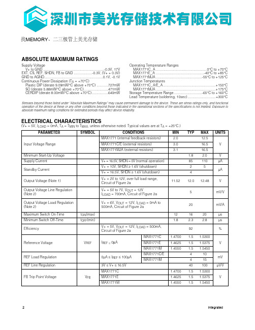
ABSOLUTE MAXIMUM RATINGSSupply VoltageV+ to GND...............................................................-0.3V, 17V EXT, CS, REF, SHDN, FB to GND...................-0.3V, (V+ + 0.3V) GND to AGND.............................................................0.1V, -0.1V Continuous Power Dissipation (T A= +70°C)Plastic DIP (derate 9.09mW/°C above +70°C)............727mW SO (derate 5.88mW/°C above +70°C).........................471mW CERDIP (derate 8.00mW/°C above +70°C).................640mW Operating Temperature RangesMAX1771C_A.....................................................0°C to +70°C MAX1771E_A..................................................-40°C to +85°C MAX1771MJA................................................-55°C to +125°C Junction TemperaturesMAX1771C_A/E_A.......................................................+150°C MAX1771MJA..............................................................+175°C Storage Temperature Range.............................-65°C to +160°C Lead Temperature (soldering, 10sec).............................+300°CStresses beyond those listed under “Absolute Maximum Ratings” may cause permanent damage to the device. These are stress ratings only, and functional operation of the device at these or any other conditions beyond those indicated in the operational sections of the specifications is not implied. Exposure to absolute maximum rating conditions for extended periods may affect device reliability.ELECTRICAL CHARACTERISTICS(V+ = 5V, I LOAD= 0mA, T A= T MIN to T MAX, unless otherwise noted. Typical values are at T A= +25°C.)2 Integrated 找MEMORY、二三极管上美光存储12V or Adjustable, High-Efficiency, Low I Q , Step-Up DC-DC ControllerELECTRICAL CHARACTERISTICS (continued)(V+ = 5V, I LOAD = 0mA, T A = T MIN to T MAX , unless otherwise noted. Typical values are at T A = +25°C.)Note 1:Output voltage guaranteed using preset voltages. See Figures 4a–4d for output current capability versus input voltage.Note 2:Output voltage line and load regulation depend on external circuit components.Typical Operating Characteristics(T A = +25°C, unless otherwise noted.)606575708085909510011010010,0001000EFFICIENCY vs. LOAD CURRENT (BOOTSTRAPED MODE)LOAD CURRENT (mA)E F F I C I E N C Y (%)606575708085909510011010010,0001000EFFICIENCY vs. LOAD CURRENT (NON-BOOTSTRAPED MODE)LOAD CURRENT (mA)E F F I C I E N C Y (%)02.00LOAD CURRENT vs.MINIMUM START-UP INPUT VOLTAGE MINIMUM START-UP INPUT VOLTAGE (V)L O A D C U R R E N T (m A )100200300400500600700 2.25 2.50 2.75 3.00 3.25 3.50MAX1771Integrated 3。
P171中文资料

P171-Type PIN/Preamp Advance Data Sheet November 2000The P171-Type PIN/Preamp features a rear-illuminated planar diode structure with low capacitance.Featuress Low-profile, 4-lead mini-DIL package:— Suitable for SONET applicationss Optional differential output in a 6-lead mini-DIL packages Transimpedance amplifier with automatic gain control (AGC)s Metal package:— Offers superior shielding for high noise immunitys High performance:— High speed (<0.5 ns typical rise and fall time)— High responsivity (0.85 A/W typical)— Low dark currents Planar structure for high reliabilitys Wavelength: 1.1 µm—1.6 µms50 µm core multimode fibers Wide operating temperature range:— –40 °C to +85 °Cs Wide bandwidths Qualification program: Telcordia Technologies* TA-NWT-983s Typical sensitivity:— –38 dBm at 155 Mbits/s— –33 dBm at 622 Mbits/sApplicationss Long-reach SONET OC-3/OC-12 and SDH STM-1/STM-4 telecommunications applicationss Secure digital data systemss Line terminal equipmentBenefitss Compact sizes Easily board mounted* Telcordia Technologies is a registered trademark of Telcordia Technologies, Inc.元器件交易网Advance Data SheetP171-Type PIN/PreampNovember 20002Agere Systems Inc.元器件交易网元器件交易网Advance Data SheetNovember 2000P171-Type PIN/Preamp元器件交易网Advance Data SheetP171-Type PIN/Preamp November 2000元器件交易网Advance Data SheetNovember 2000P171-Type PIN/Preamp元器件交易网Advance Data SheetP171-Type PIN/Preamp November 2000元器件交易网Advance Data SheetNovember 2000P171-Type PIN/PreampAdvance Data SheetP171-Type PIN/PreampNovember 2000For additional information, contact your Agere Systems Account Manager or the following:INTERNET: E-MAIL: docmaster@N. AMERICA:Agere Systems Inc., 555 Union Boulevard, Room 30L-15P-BA, Allentown, P A 18109-32861-800-372-2447 , FAX 610-712-4106 (In CANADA: 1-800-553-2448 , FAX 610-712-4106)ASIA PACIFIC:Agere Systems Singapore Pte. Ltd., 77 Science Park Drive, #03-18 Cintech III, Singapore 118256Tel. (65) 778 8833 , FAX (65) 777 7495CHINA:Agere Systems (Shanghai) Co., Ltd., 33/F Jin Mao Tower, 88 Century Boulevard Pudong, Shanghai 200121 PRCTel. (86) 21 50471212 , FAX (86) 21 50472266JAP AN:Agere Systems Japan Ltd., 7-18, Higashi-Gotanda 2-chome, Shinagawa-ku, Tokyo 141, JapanTel. (81) 3 5421 1600 , FAX (81) 3 5421 1700EUROPE:Data Requests: DATALINE: Tel. (44) 7000 582 368 , FAX (44) 1189 328 148Technical Inquiries: OPTOELECTRONICS MARKETING: (44) 1344 865 900 (Ascot UK)Agere Systems Inc. reserves the right to make changes to the product(s) or information contained herein without notice. No liability is assumed as a result of their use or application.Copyright © 2001 Agere Systems Inc.All Rights ReservedNovember 2000DS00-126OPTO-1 (Replaces DS00-126OPTO)Ordering Information*LR = meets SONET long-reach specifications.†>LR = exceeds SONET long-reach specifications.Device Code DescriptionComcode P171B014BAA 155 MHz Preamp, LR * , 4 Pins, 50 µ m Fiber, SC 108156704P171B014BAF 155 MHz Preamp, LR, 4 Pins, 50 µ m Fiber, FC/PC 108156712P171A016BAA 155 MHz Preamp, LR, 6 Pins, 50 µ m Fiber, SC 108316373P171A016BAF 155 MHz Preamp, LR, 6 Pins, 50 µ m Fiber, FC/PC 108316381P171B046BAA 622 MHz Preamp, >LR † , 6 Pins, 50 µ m Fiber, SC 108695461P171B046BAF622 MHz Preamp, >LR, 6 Pins, 50 µm Fiber, FC/PC108695479元器件交易网。
FPGA可编程逻辑器件芯片XQR2V3000-4CG717V中文规格书
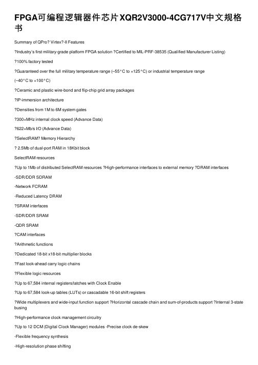
FPGA可编程逻辑器件芯⽚XQR2V3000-4CG717V中⽂规格书Summary of QPro? Virtex?-II FeaturesIndustry’s first military-grade platform FPGA solution Certified to MIL-PRF-38535 (Qualified Manufacturer Listing)100% factory testedGuaranteed over the full military temperature range (–55°C to +125°C) or industrial temperature range(–40°C to +100°C)Ceramic and plastic wire-bond and flip-chip grid array packagesIP-immersion architectureDensities from 1M to 6M system gates300+MHz internal clock speed (Advance Data)622+Mb/s I/O (Advance Data)SelectRAM Memory Hierarchy2.5Mb of dual-port RAM in 18Kbit blockSelectRAM resourcesUp to 1Mb of distributed SelectRAM resources High-performance interfaces to external memory DRAM interfaces-SDR/DDR SDRAM-Network FCRAM-Reduced Latency DRAMSRAM interfaces-SDR/DDR SRAM-QDR SRAMCAM interfacesArithmetic functionsDedicated 18-bit x18-bit multiplier blocksFast look-ahead carry logic chainsFlexible logic resourcesUp to 67,584 internal registers/latches with Clock EnableUp to 67,584 look-up tables (LUTs) or cascadable 16-bit shift registersWide multiplexers and wide-input function support Horizontal cascade chain and sum-of-products support Internal 3-state busingHigh-performance clock management circuitryUp to 12 DCM (Digital Clock Manager) modules -Precise clock de-skew-Flexible frequency synthesis-High-resolution phase shifting16 global clock multiplexer buffersActive interconnect technologyFourth-generation segmented routing structurePredictable, fast routing delay, independent offanoutSelectIO-Ultra TechnologyUp to 824 user I/Os19 single-ended and six differential standardsProgrammable sink current (2mA to 24mA) per I/ODigitally Controlled Impedance (DCI) I/O: on-chip termination resistors for single-ended I/O standards PCI compliant (32/33MHz) at 3.3VDifferential signaling622Mb/s Low-Voltage Differential Signaling I/O (LVDS) with current mode driversBus LVDS I/OLightning Data Transport (LDT) I/O with current driver buffersLow-Voltage Positive Emitter-Coupled Logic(LVPECL) I/OBuilt-in DDR input and output registersProprietary high-performance SelectLinkTechnology-High-bandwidth data path-Double Data Rate (DDR) link-Web-based HDL generation methodology ?Supported by Xilinx Foundation Series? and Alliance Series? Development SystemsIntegrated VHDL and Verilog design flowsCompilation of 10M system gates designsInternet Team Design (ITD) toolQPro Virtex-II 1.5V Platform FPGAsDS122 (v3.0) April 7, 2014Product SpecificationSlices LUTs Flip-FlopsMULT_ANDsArithmetic & Carry ChainsSOP Chains Distributed SelectRAM Shift Registers TBUF 488822128bits128bits2Table 17:Virtex-II Logic Resources Available in All CLBsDevice CLB Array: Row x Column Number of Slices Number of LUTs Max Distributed SelectRAM or Shift Register (bits) Number of Flip-Flops Number of Carry Chains (1)Number of SOP Chains (1)XQ2V100040 x 325,12010,240163,84010,2406480XQ2V300064 x 5614,33628,672458,75228,672112128XQ2V6000 96 x 8833,79267,5841,081,34467,584176192Each block SelectRAM cell is a fully synchronous memory, as illustrated in Table 31, page 38. The two ports have independent inputs and outputs and are independently clocked.Port Aspect RatiosT able 20 shows the depth and the width aspect ratios for the 18Kbit block SelectRAM. Virtex-II block SelectRAM also includes dedicated routing resources to provide an efficient interface with CLBs, block SelectRAM, and multipliers. Table 19:Dual-Port Mode ConfigurationsPort A 16K x 116K x 116K x 116K x 116K x 116K x 1Port B16K x 18K x 24K x 42K x 91K x 18512x 36Port A8K x 28K x 28K x 28K x 28K x 2Port B8K x 24K x 42K x 91K x 18512x 36Port A4K x 44K x 44K x 44K x 4Port B4K x 42K x 91K x 18512x 36Port A2K x 92K x 92K x 9Port B 2K x 91K x 18512x 36Port A 1K x 181K x 18Port B 1K x 18512x 36Port A 512x 36Port B512x 36Figure 31:18 Kbit Block SelectRAM in Dual-Port ModeTable 20:18Kbit Block SelectRAM Port Aspect RatioWidth Depth Address Bus Data Bus Parity Bus116,384ADDR[13:0]DA T A[0]N/A 28,192ADDR[12:0]DA TA[1:0]N/A 44,096ADDR[11:0]DA TA[3:0]N/A 92,048ADDR[10:0]DA TA[7:0]Parity[0]181,024ADDR[9:0]DA TA[15:0]Parity[1:0]36512ADDR[8:0]DA TA[31:0]Parity[3:0]。
IAC-IMX8MP-KIT 嵌入式开发板硬件说明书

IAC-IMX8MP-KIT 嵌入式开发板硬件说明书版本号:V 1.02021年08月浙江启扬智能科技有限公司版权所有QIYANG TECHNOLOGY Co., LtdCopyright Reserved有任何技术问题或需要帮助,请联系:*********************** 第2页 共38页 购买产品,请联系销售:********************更多信息请访问: 技术支持如果您对文档有疑问,可在办公时间(周一至周五 8:30-12:00,13:30-17:30),通过以 下方式联系我们:技术邮箱:***********************技术支持电话:*************-805官网:(中文)/(英文)资料更新与获取1、资料的更新产品相关资料会不断完善更新;当您在使用这些内容时,请确保其为最新状态。
2、更新通知启扬智能产品资料更新通过微信公众号进行推送通知,敬请关注!3、资料如何获取产品购买后,请联系我公司相关销售人员获取。
有任何技术问题或需要帮助,请联系:*********************** 第3页 共38页 购买产品,请联系销售:********************更多信息请访问: 版本更新记录有任何技术问题或需要帮助,请联系:*********************** 第4页 共38页 购买产品,请联系销售:******************** 目 录阅读前须知:本手册主要介绍该开发板的硬件接口............................................................................................ 5 一、前言 . (5)1.1、公司简介 .................................................................................................................................................. 5 1.2、IAC-IMX8MP-KIT 开发/评估板的使用建议 ........................................................................................ 5 二、系统组成 .. (6)2.1、芯片概述 .................................................................................................................................................. 6 2.2、开发板资源 ............................................................................................................................................ 10 2.3、核心板资源 ............................................................................................................................................ 12 三、底板接口功能 . (13)3.1、基本接口功用说明 ................................................................................................................................ 15 3.2、跳线拨码设置 ........................................................................................................................................ 17 3.3、接口引脚定义 ........................................................................................................................................ 18 四、尺寸结构图 .. (33)4.1、核心板尺寸 ............................................................................................................................................ 33 4.2、底板尺寸 ................................................................................................................................................ 34 五、器件连接示图 ................................................................................................................................................. 35 六、电气特性 ......................................................................................................................................................... 36 六、软件描述 ......................................................................................................................................................... 37 七、附注 .. (37)有任何技术问题或需要帮助,请联系:*********************** 第5页 共38页 购买产品,请联系销售:********************阅读前须知:本手册主要介绍该开发板的硬件接口 一、前言1.1、公司简介浙江启扬智能科技有限公司2007年成立于杭州, 是一家专注于ARM 嵌入式产品研发、生产与销售的国家高新技术企业。
NC7SV17中文资料

元器件交易网
NC7SV17
Logic Symbol
IEEE/IEC
Connection Diagrams
Pin Assignments for SC70
Pin Descriptions
Pin Name A Y NC Description Input Output No Connect Pad Assignments for MicroPak (Top View)
±24 mA @ 3.00V VCC ±18 mA @ 2.30V VCC ±6 mA 1.4V VCC @ 1.1V VCC
±0.1 mA @ 0.9V VCC
s Uses patented Quiet Series noise/EMI reduction circuitry s Ultra small MicroPak leadfree package s Ultra low dynamic power
Function Table
Y=A Input A L H
H = HIGH Logic Level L = LOW Logic Level
Output Y L H (Top Thru View)
2
元器件交易网
NC7SV17
Absolute Maximum Ratings(Note 1)
Ordering Code:
Order Number NC7SV17P5X NC7SV17L6X Package Number MAA05A MAC06A Product Code Top Mark V17 G5 Package Description 5-Lead SC70, EIAJ SC-88a, 1.25mm Wide 6-Lead MicroPak, 1.0mm Wide Supplied As 3k Units on Tape and Reel 5k Units on Tape and Reel
IMX1T110中文资料
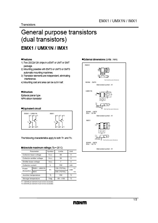
Transistors1/3General purpose transistors (dual transistors)EMX1 / UMX1N / IMX1!Features1) Two 2SC2412K chips in a EMT or UMT or SMT package.2) Mounting possible with EMT3 or UMT3 or SMT3automatic mounting machines.3) Transistor elements are independent, eliminating interference.4) Mounting cost and area can be cut in half.!StructureEpitaxial planar type NPN silicon transistor!Equivalent circuitThe following characteristics apply to both Tr 1 and Tr 2.!Absolute maximum ratings (T a = 25°C)ParameterSymbol Limits Unit V CBO 60V 50V V V CEO V EBO 7I C mA 150Tj 150˚C Tstg−55∼+150˚CP C EMX1, UMX1N 150 (TOTAL)mW IMX1300 (TOTAL)∗1∗2Collector-base voltage Collector-emitter voltage Emitter-base voltage Collector currentJunction temperature Storage temperaturePowerdissipation ∗1 120mW per element must not be exceeded.∗2 200mW per element must not be exceeded.!External dimensions (Units : mm)Transistors2/3!Electrical characteristics (T a = 25°C)ParameterSymbol BV CBO BV CEO BV EBO I CBO I EBO h FE V CE (sat)CobMin.60507−−120−−−−−−−−−2−−−0.10.15600.43.5V I C =50µA I C =1mA I E =50µA V CB =60V V EB =7V V CE =6V, IC =1mAI C /I B =50mA/5mA V V µA µA −V PFTyp.Max.Unit Conditionsf T −180−V CE =12V, I E =−2mA, f =100MHzV CB =12V, I E =0A, f =1MHzMHz ∗Collector-base breakdown voltage Collector-emitter breakdown voltage Emitter-base breakdown voltage Collector cutoff current Emitter cutoff currentDC current transfer ratio Transition frequency Collector-emitter saturation voltage Output capacitance!Electrical characteristic curvesC O L L E C T O R C U R R E N T : I C (m A )BASE TO EMITTER VOLTAGE : VBE (V)Fig.1 Grounded emitter propagationcharacteristicsC O L L E C T O R C U R R E N T : I C (m A )COLLECTOR TO EMITTER VOLTAGE : V CE (V)Fig.2 Grounded emitter outputcharacteristics ( I )C O L L E C T O R C U R R E N T : I C (m A )COLLECTOR TO EMITTER VOLTAGE : V CE (V)Fig.3 Grounded emitter output characteristics ( II )Transistors3/3D C C U R RE N T G A I N : hF ECOLLECTOR CURRENT : I C (mA)Fig.4 DC current gain vs. collector current ( I )D C C U R RE N T G A I N : hF ECOLLECTOR CURRENT : I C (mA)Fig.5 DC current gain vs. collector current ( II )C O L L E C T O R S A T U R A T I O N V O L T A G E : V C E (s a t ) (V )COLLECTOR CURRENT : I C (mA)Fig.6 Collector-emitter saturationvoltage vs. collector currentC O L L E C T O R S A T U R A T I O N V O L T A G E : V C E (s a t ) (V )COLLECTOR CURRENT : I C (mA)Fig.7 Collector-emitter saturation voltage vs. collector current ( I )C O L L E C T O R S A T U R A T I O N V O L T A G E : V C E (s a t ) (V )COLLECTOR CURRENT : I C (mA)Fig.8 Collector-emitter saturationvoltage vs. collector current ( II )C O L L E C T O R S A T U R A T I O N V O L T A G E : V C E (s a t ) (V )COLLECTOR CURRENT : I C (mA)Fig.9 Collector-emitter saturationvoltage vs. collector current ( III )EMITTER CURRENT : I E (mA)T R A N S I T I O N F R E Q U E N C Y : f T (M H z )Fig.10 Gain bandwidth product vs. emitter currentCOLLECTOR TO BASE VOLTAGE : V CB (V)EMITTER TO BASE VOLTAGE : V EB (V)C O L L EC T O R O U T P U T C A P A C I T A N C E : C o b (p F )E M I T T E R I N P U T C A P A C I T A N C E : C i b (p F )Fig.11 Collector output capacitance vs. collector-base voltageEmitter input capacitance vs. emitter-base voltage−EMITTER CURRENT : I E (mA)Fig.12 Base-collector time constant vs.emitter currentB A S EC O L L E C T O R T I M E C O N S T A N T : C c r b b (p s )AppendixAbout Export Control Order in JapanProducts described herein are the objects of controlled goods in Annex 1 (Item 16) of Export Trade ControlOrder in Japan.In case of export from Japan, please confirm if it applies to "objective" criteria or an "informed" (by MITI clause)on the basis of "catch all controls for Non-Proliferation of Weapons of Mass Destruction.Appendix1-Rev1.0。
XQR17V16VQ44N中文资料
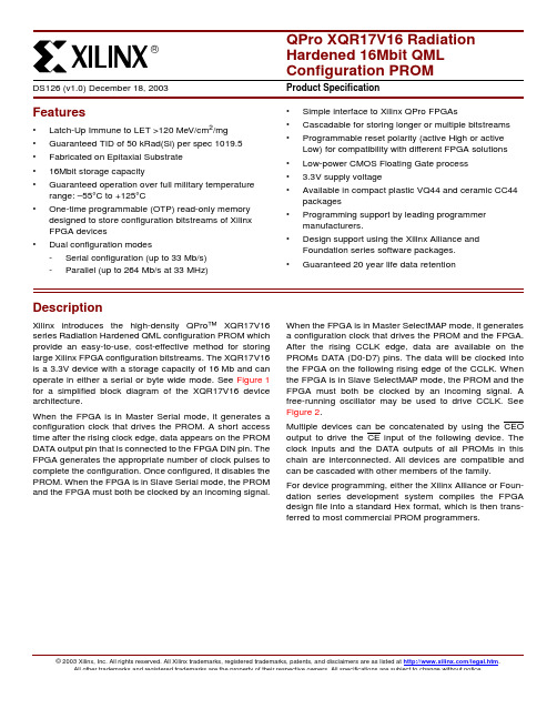
© 2003 Xilinx, Inc. All rights reserved. All Xilinx trademarks, registered trademarks, patents, and disclaimers are as listed at /legal.htm .All other trademarks and registered trademarks are the property of their respective owners. All specifications are subject to change without notice.Features•Latch-Up Immune to LET >120 MeV/cm 2/mg •Guaranteed TID of 50 kRad(Si) per spec 1019.5•Fabricated on Epitaxial Substrate •16Mbit storage capacity•Guaranteed operation over full military temperature range: –55°C to +125°C•One-time programmable (OTP) read-only memory designed to store configuration bitstreams of Xilinx FPGA devices•Dual configuration modes -Serial configuration (up to 33Mb/s)-Parallel (up to 264Mb/s at 33MHz)•Simple interface to Xilinx QPro FPGAs•Cascadable for storing longer or multiple bitstreams •Programmable reset polarity (active High or active Low) for compatibility with different FPGA solutions •Low-power CMOS Floating Gate process • 3.3V supply voltage•Available in compact plastic VQ44 and ceramic CC44 packages•Programming support by leading programmer manufacturers.•Design support using the Xilinx Alliance and Foundation series software packages.•Guaranteed 20 year life data retentionDescriptionXilinx introduces the high-density QPro™ XQR17V16series Radiation Hardened QML configuration PROM which provide an easy-to-use, cost-effective method for storing large Xilinx FPGA configuration bitstreams. The XQR17V16is a 3.3V device with a storage capacity of 16Mb and can operate in either a serial or byte wide mode. See Figure 1for a simplified block diagram of the XQR17V16 device architecture.When the FPGA is in Master Serial mode, it generates a configuration clock that drives the PROM. A short access time after the rising clock edge, data appears on the PROM DATA output pin that is connected to the FPGA DIN pin. The FPGA generates the appropriate number of clock pulses to complete the configuration. Once configured, it disables the PROM. When the FPGA is in Slave Serial mode, the PROM and the FPGA must both be clocked by an incoming signal.When the FPGA is in Master SelectMAP mode, it generates a configuration clock that drives the PROM and the FPGA.After the rising CCLK edge, data are available on the PROMs DATA (D0-D7) pins. The data will be clocked into the FPGA on the following rising edge of the CCLK. When the FPGA is in Slave SelectMAP mode, the PROM and the FPGA must both be clocked by an incoming signal. A free-running oscillator may be used to drive CCLK. See Figure 2.Multiple devices can be concatenated by using the CEO output to drive the CE input of the following device. The clock inputs and the DATA outputs of all PROMs in this chain are interconnected. All devices are compatible and can be cascaded with other members of the family.For device programming, either the Xilinx Alliance or Foun-dation series development system compiles the FPGA design file into a standard Hex format, which is then trans-ferred to most commercial PROM programmers.QPro XQR17V16 Radiation Hardened 16Mbit QML Configuration PROMDS126 (v1.0) December 18, 2003Product SpecificationPin DescriptionDATA[0:7]Data output is in a high-impedance state when either CE or OE are inactive. During programming, the D0 pin is I/O. Note that OE can be programmed to be either active High or active Low.CLKEach rising edge on the CLK input increments the internal address counter, if both CE and OE are active.RESET/OEWhen High, this input holds the address counter reset and puts the DATA output in a high-impedance state. The polar-ity of this input pin is programmable as either RESET/OE or OE/RESET. To avoid confusion, this document describes the pin as RESET/OE, although the opposite polarity is pos-sible on all devices. When RESET is active, the address counter is held at “0”, and puts the DATA output in a high-impedance state. The polarity of this input is program-mable. The default is active High RESET, but the preferred option is active Low RESET, because it can connected to the FPGAs INIT pin and a pullup resistor.The polarity of this pin is controlled in the programmer inter-face. This input pin is easily inverted using the Xilinx HW-130 Programmer. Third-party programmers have differ-ent methods to invert this pin.CEWhen High, this pin disables the internal address counter, puts the DATA output in a high-impedance state, and forces the device into low-I CC standby mode.CEOChip Enable output, to be connected to the CE input of the next PROM in the daisy chain. This output is Low when the CE and OE inputs are both active AND the internal address counter has been incremented beyond its Terminal Count (TC) value. In other words: when the PROM has been read, CEO will follow CE as long as OE is active. When OE goes inactive, CEO stays High until the PROM is reset. Note that OE can be programmed to be either active High or active Low.Figure 1: Simplified Block Diagram for XQR17V16 (does not show programming circuit)BUSY (XQR17V16 only)If BUSY pin is floating, the user must program the BUSY bit which will cause BUSY pin to be internally tied to apull-down resistor. When asserted High, output data are held and when BUSY pin goes Low, data output will resume.V PPProgramming voltage. No overshoot above the specified max voltage is permitted on this pin. For normal read oper-ation, this pin must be connected to V CC. Failure to do so may lead to unpredictable, temperature-dependent opera-tion and severe problems in circuit debugging. Do not leave V PP floating!V CC and GNDPositive supply and ground pins.PROM Pinouts for XQR17V16(Pins not listed are “no connect”)CapacityControlling PROMsConnecting the FPGA device with the PROM.•The DATA output(s) of the PROM(s) drives the D IN input of the lead FPGA device.•The Master FPGA CCLK output drives the CLK input(s) of the PROM(s).•The CEO output of a PROM drives the CE input of the next PROM in a daisy chain (if any).•The RESET/OE input of all PROMs is best driven by the INIT output of the lead FPGA device. Thisconnection assures that the PROM address counter is reset before the start of any (re)configuration, evenwhen a reconfiguration is initiated by a V CC glitch. •The PROM CE input is best connected to the FPGA DONE pin(s) and a pullup resistor. CE can also bepermanently tied Low, but this keeps the DATA output active and causes an unnecessary supply current of15mA maximum.•SelectMAP mode is similar to Slave Serial mode. The DATA is clocked out of the PROM one byte per CCLK instead of one bit per CCLK cycle. See FPGA datasheets for special configuration requirements.FPGA Master Serial Mode SummaryThe I/O and logic functions of the Configurable Logic Block (CLB) and their associated interconnections are estab-lished by a configuration program. The program is loaded either automatically upon power up, or on command, depending on the state of the three FPGA mode pins. In Master Serial mode, the FPGA automatically loads the con-figuration program from an external memory. The Xilinx PROMs have been designed for compatibility with the Mas-ter Serial mode.Upon power-up or reconfiguration, an FPGA enters the Master Serial mode whenever all three of the FPGAPin Name44-pin VQFP44-pin CLCC BUSY2430D0402D12935D2424D32733D4915D52531D61420D71925CLK435 RESET/OE(OE/RESET)1319CE1521GND6, 18, 28, 37, 413, 12, 24, 34, 43 CEO2127V PP3541V CC8, 16, 17, 26, 36,3814, 22, 23, 32,42, 44Device Configuration BitsXQR17V1616,777,216Xilinx FPGAs and Compatible PROMsDevice Configuration Bits XQR17V16(s)XQR2V10004,082,6561XQR2V300010,494,4321XQR2V600021,849, 5682XQVR3001,751,8081XQVR6003,607,9681XQVR10006,127,7441mode-select pins are Low (M0=0, M1=0, M2=0). Data is read from the PROM sequentially on a single data line. Syn-chronization is provided by the rising edge of the temporary signal CCLK, which is generated during configuration. Master Serial Mode provides a simple configuration inter-face. Only a serial data line, two control lines, and a clock line are required to configure an FPGA. Data from the PROM is read sequentially, accessed via the internal address and bit counters which are incremented on every valid rising edge of CCLK.If the user-programmable, dual-function DIN pin on the FPGA is used only for configuration, it must still be held at a defined level during normal operation. The Xilinx FPGA families take care of this automatically with an on-chip default pull-up/down resistor or keeper circuit. Cascading Configuration PROMsFor multiple FPGAs configured as a daisy-chain, or for future FPGAs requiring larger configuration memories, cas-caded PROMs provide additional memory. After the last bit from the first PROM is read, the next clock signal to the PROM asserts its CEO output Low and disables its DATA line. The second PROM recognizes the Low level on its CE input and enables its DATA output. See Figure2.After configuration is complete, the address counters of all cascaded PROMs are reset if the FPGA PROGRAM pin goes Low, assuming the PROM reset polarity option has been inverted.Figure 2: (a) Master Serial Mode (b) Virtex SelectMAP Mode (dotted lines indicates optional connection)Standby ModeThe PROM enters a low-power standby mode whenever CE is asserted High. The output remains in a high imped-ance state regardless of the state of the OE input.ProgrammingThe devices can be programmed on programmers supplied by Xilinx or qualified third-party vendors. The user must ensure that the appropriate programming algorithm and the latest version of the programmer software are used. The wrong choice can permanently damage the device.Radiation TolerancesTable 1: Truth Table for XQ17V00 Control InputsControl Inputs Internal AddressOutputs RESET CE DATA CEO I CC Inactive Low If address < TC (1): increment If address > TC (1): don’t changeActive High-Z High Low Active Reduced Active Low Held reset High-Z High Active Inactive High Not changing High-Z High Standby ActiveHighHeld resetHigh-ZHighStandbyNotes:1.The XQ17V00 RESET input has programmable polarity1.TC = Terminal Count = highest address value. TC + 1 = address 0.Table 2: Guaranteed Radiation Tolerance Specifications (1)Symbol DescriptionMin Max Units TID Total Ionizing Dose for data retention and data output port read (configuration) operations -50krad(Si)SEL Single Event Latch-Up(No Latch-Up observed for LET > 120 MeV-mg/cm 2)-0cm 2SEUStatic Memory Cell Saturation Bit Cross-Section (No Upset observed for LET > 120 MeV-mg/cm 2)-cm 2Notes:1.For more information on dynamic SEU error rates please see the SEU test reports at /milaeroAbsolute Maximum RatingsOperating Conditions (3.3V Supply)DC Characteristics Over Operating ConditionSymbol DescriptionConditions Units V CC Supply voltage relative to GND –0.5 to +7.0V V PP Supply voltage relative to GND –0.5 to +12.5V V IN Input voltage relative to GND –0.5 to V CC +0.5V V TS Voltage applied to High-Z output –0.5 to V CC +0.5V T STG Storage temperature (ambient)–65 to +150°C T SOL Maximum soldering temperature (10s @ 1/16 in.)+260°C T JJunction temperatureCeramic +150°C Plastic+125°CNotes:1.Stresses beyond those listed under Absolute Maximum Ratings may cause permanent damage to the device. These are stressratings only, and functional operation of the device at these or any other conditions beyond those listed under Operating Conditions is not implied. Exposure to Absolute Maximum Ratings conditions for extended periods of time may affect device reliability.Symbol DescriptionMin Max Units V CC (1)Supply voltage relative to GND (T C = –55°C to +125°C)Ceramic 3.0 3.6V Supply voltage relative to GND (T J = –55°C to +125°C)Plastic3.0 3.6V T VCCV CC rise time from 0V to nominal voltage1.050msNotes:1.During normal read operation V PP must be connected to V CC.2.At power up, the device requires the V CC power supply to monotonically rise from 0V to nominal voltage within the specified V CC risetime. If the power supply cannot meet this requirement, then the device may not power-on-reset properly.Symbol DescriptionMin Max Units V IH High-level input voltage 2V CC V V IL Low-level input voltage00.8V V OH High-level output voltage (I OH = –3 mA) 2.4-V V OL Low-level output voltage (I OL = +3 mA)-0.4V I CCA Supply current, active mode (at maximum frequency) -100mA I CCS Supply current, standby mode -1mA I L Input or output leakage current–1010µA C IN Input capacitance (V IN = GND, f = 1.0 MHz)-15pF C OUTOutput capacitance (V IN = GND, f = 1.0 MHz)-15pFAC Characteristics Over Operating Condition for XQR17V16Symbol Description Min Max Units T OE OE to data delay-15ns T CE CE to data delay-20ns T CAC CLK to data delay(2)-20ns T DF CE or OE to data float delay(3,4)-35ns T OH Data hold from CE, OE, or CLK(4)0-ns T CYC Clock periods50-ns T LC CLK Low time(4)25-ns T HC CLK High time(4)25-ns T SCE CE setup time to CLK (to guarantee proper counting)25-ns T HCE CE hold time to CLK (to guarantee proper counting)0-ns T HOE OE hold time (guarantees counters are reset)25-ns T SBUSY BUSY setup time5-ns T HBUSY BUSY hold time5-ns Notes:1.AC test load = 50 pF.2.When BUSY = 0.3.Float delays are measured with 5 pF AC loads. Transition is measured at ±200 mV from steady state active levels.4.Guaranteed by design, not tested.5.All AC parameters are measured with V IL = 0.0V and V IH = 3.0V.AC Characteristics Over Operating Condition When CascadingSymbol DescriptionMin Max Units T CDF CLK to data float delay (2,3)-50ns T OCK CLK to CEO delay (3)-30ns T OCE CE to CEO delay (3)-35ns T OOERESET/OE to CEO delay (3)-30nsNotes:1.AC test load = 50 pF2.Float delays are measured with 5 pF AC loads. Transition is measured at ±200 mV from steadystate active levels.3.Guaranteed by design, not tested.4.All AC parameters are measured with V IL = 0.0V and V IH= 3.0V.Ordering InformationRevision HistoryThe following table shows the revision history for this document.Date Version Revision12/15/031.0Initial Xilinx release.XQR17V16 CC44 VManufacturing GradePackage TypeDevice NumberDevice Ordering OptionsDevice Type PackageGradeFlowTempXQR17V16CC4444-pin Ceramic Chip Carrier Package M M-Grade Military Ceramic T C = –55°C to +125°CVQ4444-pin Plastic Thin Quad Flat PackageV QPRO-PLUS N Class NMilitary Plastic T J = –55°C to +125°CRQPRO+PLUS PEMValid Ordering CombinationsM Grade V Grade N Grade R Grade XQR17V16CC44MXQR17V16CC44VXQR17V16VQ44NXQR17V16VQ44R。
索尼IMX264LLR IMX264LQR传感器模块数据手册说明书

FSM-IMX264 DatasheetSony IMX264LLR / IMX264LQR Sensor ModuleFRAMOS Sensor ModuleKey Benefits & Features:▪ 5.1 Mpx Sony CMOS Global Shutter sensormodule, ready to embed!▪ All FSMs are part of a rapid prototypingecosystem, consisting of:✓ Adapters to various processing boards ✓ Design sources for deep embedding✓ Various accessories and design in servicesFSM-IMX264M (Monochrome):FSM-IMX264C (Color):Pin 1 according to print on PCB.Mechanical DrawingSensor image optical center is in mechanical board center.Connector PinoutType: Hirose DF40C-60DP-0.4V(51)Mating Type: Hirose DF40HC(4.0)-60DS-0.4V(51)N a m eN C N C 3V 3 3V 3 1V 8G N DG N DS D AS D O T O U T 0T O U T 1T O U T 2N CN CN CG N DR S TM C L KG N DD _D A T A _6_PD _D A T A _6_NG N DD _D A T A _4_PD _D A T A _4_NG N DD _D A T A _2_PD _D A T A _2_NG N D D _D A T A _0_P D _D A T A _0_N Pin 1 3 5 7 9 11 13 15 17 19 21 23 25 27 29 31 33 35 37 39 41 43 45 47 49 51 53 55 57 59Pin 2 4 6 8 10 12 14 16 18 20 22 24 26 28 30 32 34 36 38 40 42 44 46 48 50 52 54 56 58 60N a m e1V 8_E E P R O M 1V 8_E E P R O M 1V 2 1V 2 N CG N DG N DS C LX C ES L A M O D EX M A S T E RN CX T R I GX H SX V SG N DD _D A T A _7_PD _D A T A _7_NG N DD _D A T A _5_PD _D A T A _5_NG N DD _D A T A _3_PD _D A T A _3_NG N DD _D A T A _1_PD _D A T A _1_NG N DD _C L K _0_PD _C L K _0_NSignals are routed directly from image sensor to connector. Details on specific signals are described in the respective image sensor datasheet.Table of Contents1 FRAMOS Sensor Module Ecosystem (2)1.1 Ecosystem Overview (3)1.2 Materials and Services (4)2 Software Package and Drivers (5)2.1 Reference Software: NVIDIA Jetson Family (6)2.1.1 Platform and Sensor Device Drivers (6)2.1.2 Image Pre-Processing Examples (7)3 Ecosystem Compatibility Matrix (10)3.1 Hardware Support (10)1FRAMOS Sensor Module EcosystemThe FSM Ecosystem consists of FRAMOS Sensor Modules, Adapters, Software and Sources, and provides one coherent solution supporting the whole process of integrating image sensors into embedded vision products.During the evaluation and proof-of-concept phase, off-the-shelf sensor modules with a versatile adapter framework allow the connection of latest image sensor technology to open processing platforms, like the NVIDIA Jetson Family or the standard. Reference drivers and sample applications deliver images immediately after installation, supporting V4L2 and an optional derivate API providing comfortable integration. Within the development phase, electrical design references and driver sources guide with a solid and proven baseline to quickly port into individual system designs and extend scope, while decreasing risk and efforts.To simplify and relieve the whole supply chain, all FRAMOS Sensor Modules and adapters are optimized and ready for delivery in volume and customization with pre-configured lens holder, lens and further accessories.Off-the-Shelf Hardware▪FRAMOS Sensor Modules (FSM) from stock, ready for evaluation and optimized for initial mass production.▪Versatile adapter framework, allowing flexible testing of different modules, ondifferent processing boards:▪FRAMOS Sensor Adapter (FSA):Everything the specific sensor needs foroperation▪FRAMOS Processor Adapter (FPA):Connect up to four FSM + FSA to aspecific processor board▪From lenses, mechanics and cables, all needed imaging accessories from one hand Ready to go Software Package▪Drivers with basic sensor integration:▪Platform specific device drivers▪V4L2 subdevice drivers for specific image sensors (low-level C API)▪Streamlined V4L2 library (LibSV) withcomfortable and generic C/C++ API▪Example applications demonstratinginitialization, main configuration and imagestream processingFurther to the off-the-shelf hard- and software, the Ecosystem supports you on project basis with:▪Driver sources allowing the focus on application specific scope and sensor features▪Electrical references for FSA and FPA, supporting quick and optimized embedding of FSMs▪Engineering services via FRAMOS and its partners, allowing you to focus on your produ ct’s unique value1.1 Ecosystem OverviewThe figure below shows a map of compatibility with all components inside the Ecosystem. Every element (orhardware) and connection displayed in Green operates with native MIPI CSI-2 (D-PHY) data.Every component and connection displayed in Orange or Blue operates with proprietary (Sub-LVDS, SLVS) or standardized (SLVS-EC) LVDS data, that requires further attention to the physical processing of the image data by either data conversion or specific FPGA IP. Users of MIPI CSI-2 based processing systems are supported by FSM specific data conversion located on dedicated FRAMOS Sensor Adapters (FSAs).Figure 1: Assembly of a typical Sensor Module Development KitSpecification and compatibility of all individual components are listed in the appropriate chapter of the full datasheet. Access to software and drivers is only granted with the purchase of the appropriate development kit. Electrical design sources, support and services are provided on individual basis, they are not part of the development kit or component purchase.Flex Cable Sensor Module (FSM) Sensor Adapter (FSA)Processor Adapter(FPA)Lens Mount1.2Materials and ServicesBelow you can find a list of materials and services as part of the FRAMOS Sensor Module Ecosystem. Hardware▪FRAMOS Sensor Module Development Kits▪Individual Parts:▪FRAMOS Sensor Modules▪FRAMOS Sensor Adapters▪FRAMOS Processor Adapters▪FRAMOS Module Accessories (Cables, Mounts)Software (part of the Development Kit)▪Software Package for NVIDIA Jetson AGX Xavier, Nano, TX2 and Xavier NX▪Software Package for DragonBoard 410c (96Boards)▪Xilinx FPGA reference implementation for SLVS-EC (Sony IMX421, IMX530)Design Sources (on Project Basis)▪Software Driver Sources▪Electrical References for FSA, FPA (Schematics)Design Services▪Off-the-shelf hardware customization including size, shape, connector and extended functionality ▪Software customization and extension▪Additional processor board support▪Further sensor features and image (pre-)processing▪Integration of additional sensors▪Optimization for volume production▪Lens assembly and alignment▪System / solution development▪Production and integration2Software Package and DriversAs FRAMOS we know that the getting started with a new technology is the biggest challenge. The idea behind the Software Package is to enable embedded software engineers to get quickly to a streaming system and provide at the same time all tools that are needed to extend and adapt it according the individual needs of the application.What the software package and driver are:▪ A reference for a custom sensor implementation▪Demonstrating how to use the required interfaces▪Demonstrating how to communicate with the image sensor▪Demonstrating how to generaly initialize and configure the image sensor▪Provide initial image streaming output to the user space▪Demonstrating how to run basic image processing on pixel dataWhat it is not:▪ A fully featured camera implementation - not all sensors features might be implemented▪Ready to be use in the field▪ A benchmark for the capabilities of the image sensor▪Focused on image processingSupported Processor PlatformsThe table below shows which platforms are supported by the standard driver package, and how many FSMs can at maximum be operated in parallel.2.1Reference Software: NVIDIA Jetson FamilyThe software package provided with the Development Kits of the FRAMOS Sensor Module Ecosystem provided for NVIDIA Jetson platforms provides a reference implementation of sensor and device drivers for MIPI CSI-2. It contains a minimum feature set demonstrating how to utilize the platform specific data interface and communication implementation, as well as the initialization of the image sensor and implementation of basic features.Package Content:▪Platform and device drivers with Linux for Tegra Support▪V4L2 based subdevice drivers (low-level C API)▪Streamlined V4L2 library (LibSV) providing generic C/C++ API▪Image Pre-Processing Examples:▪OpenCV (Software)▪LibArgus (Hardware)Supported Devices:▪Jetson Nano (B01)▪Jetson TX2▪Jetson Xavier NX▪Jetson AGX Xavier2.1.1Platform and Sensor Device DriversThe driver divides into two main parts that are configured in separate ways – the Image Modes and the General Features of the image sensor.Image ModesThese are major attributes that have impact to the image data stream formatting. They require a static pre-configuration within the device tree (DT):▪Image / streaming resolution▪Pixel format / bit depth▪Data rate / lane configurationEach driver provides access to 3 –5 pre-built configurations, reflecting the main operation modes of the imager. Beside the full resolution, that is always available, they allow to receive image streams in common video resolutions like VGA, Full HD and UHD as they are supported or make sense by the imagers, and utilize sensor features like ROI and binning.They act as an example for implementation and usage and are available as source. Due to the size limitation of the device tree, it is not possible to integrate an extensive set of options.General FeaturesThese are attributes of the image sensor that do not manipulate the data stream formatting. The drivers provided with the Software Pack integrate the sensor features as shown in the table below.Pre-Implemented Features per ModelG a i n (A n a l o g / D i g i t a l )F r a m e R a t eE x p o s u r e T i m eF l i p / M i r r o rI S M o d e (M a s t e r / S l a v e )S e n s o r M o d e I DT e s t P a t t e r n O u t p u tB l a c k L e v e lH D R O u t p u tB r o a d c a s tD a t a R a t eS y n c h r o n i z i n g M a s t e rFSM-AR0144 FSM-AR0521 FSM-AR1335 FSM-HDP230 FSM-IMX264 FSM-IMX283 FSM-IMX290 FSM-IMX296 * FSM-IMX297 * FSM-IMX304 FSM-IMX327 FSM-IMX334 FSM-IMX335 FSM-IMX412 FSM-IMX415 FSM-IMX462 FSM-IMX464 FSM-IMX477 FSM-IMX485 FSM-IMX530FSM-IMX577Table 2: Supported sensor features on NVIDIA Jetson TX2 / AGX XavierFurther features, as been supported by the image sensor, can be integrated into the driver sources using the image sensor datasheet.2.1.2 Image Pre-Processing ExamplesThe provided image processing examples show the general mechanisms of data handling, for an image processing using 3rd -party IP. Both, the OpenCV and the LibArgus examples do not output data that is tuned for best visual experience.LibArgus Example:▪ Closed source ISP implementation ▪ Using hard ISP in NVIDIA Jetson SOCs ▪ Most performant option▪ Example Implementation: Full but not tuned image pipeline, displaying Not ImplementedV4L (libsv)V4L (libsv) and libargus *Only supported in all pixel modeColor tuning and lens correction needs to be calibrated for every image sensor separately and depends onsensor and lens attributes as well as illumination situation.Image Pre-Processing Features per ModelB a d P i x e lC o r r e c t i o nN o i s e R e d u c t i o nB l a c k L e v e lC o m p .A u t o E x p o s u r e , G a i nA u t o W h i t eB a l a n c eD e m o s a i cC o l o r C o r r e c t i o nC o l o r A r t i f a c t S u p p r .D o w n s c a l i n gE d g e E n h a n c e m e n tFSM-AR0144 FSM-AR0521 FSM-AR1335 FSM-HDP230 FSM-IMX264 FSM-IMX283 FSM-IMX290 FSM-IMX296 FSM-IMX297 FSM-IMX304 FSM-IMX327 FSM-IMX334 FSM-IMX335 FSM-IMX412 FSM-IMX415 FSM-IMX462 FSM-IMX464 FSM-IMX477 FSM-IMX485 FSM-IMX530FSM-IMX577Table 3: Implemented LibArgus features for NVIDIA Jetson TX2 / AGX XavierDefault ConfigImage streaming is performed through the LibArgus pipeline, using a common configuration. It demonstrates the usage of LibArgus but is not optimized for the certain sensor configuration and might not lead to good image representation.As NVIDIA camera partner, FRAMOS provides appropriate ISP tuning services on project basis for the individual customer system.Not ImplementedImplementedUsing Default Config9 OpenCV Example:▪ Open software library▪ Easy to use and large feature set ▪ Extremely performance hungry (CPU) ▪ Not recommended for pre-processing▪ Example Implementation: Demosaicing, DisplayingImage Pre-Processing Features per ModelB a d P i x e lC o r r e c t i o nN o i s e R e d u c t i o nB l a c k L e v e lC o m p . A u t o E x p o s u r e , G a i nA u t o W h i t eB a l a n c eD e m o s a i cC o l o r C o r r e c t i o nC o l o r A r t i f a c t S u p p r .D o w n s c a l i n gE d g e E n h a n c e m e n tFSM-AR0144 FSM-AR0521 FSM-AR1335 FSM-HDP230 FSM-IMX264 FSM-IMX283 FSM-IMX290 FSM-IMX296 FSM-IMX297 FSM-IMX304 FSM-IMX327 FSM-IMX334 FSM-IMX335 FSM-IMX412 FSM-IMX415 FSM-IMX462 FSM-IMX464 FSM-IMX477 FSM-IMX485 FSM-IMX530FSM-IMX577Table 4: Implemented features in OpenCV exampleDue to limited performance and extreme resource utilization, it is not planned to enhance the image processing support on software side.Not ImplementedImplemented10 3 Ecosystem Compatibility Matrix3.1 Hardware SupportThe following matrix shows the compatibility of FSMs, FSAs and FPAs to each other. The FSAs differentiate toeach other by supplied voltages, power up sequence, generated clock (oscillator) and physical attributes.2Not verified, Xilinx Development Board with hard MIPI CSI-2 / D-PHY interface. 3FSM-IMX334 is not supported due to the sensor requiring 4-lanes MIPI.11。
TSOP17XX中文资料
0.6
0.4 0.2 0.0 0.8 0.9 1.0 1.1 1.2 1.3 f / f0 – Relative Frequency
Df ( 3 dB ) = f0 / 10
f = f0
"5%
eE min
0.0
94 8147
0.4
0.8
1.2
1.6
2.0
E – Field Strength of Disturbance ( kV / m )
元器件交易网
TSOP17..
Vishay Telefunken
Photo Modules for PCM Remote Control Systems
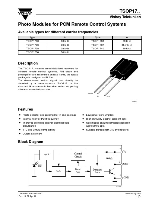
Available types for different carrier frequencies
Type TSOP1730 TSOP1736 TSOP1738 TSOP1756 fo 30 kHz 36 kHz 38 kHz 56 kHz Type TSOP1733 TSOP1737 TSOP1740 fo 33 kHz 36.7 kHz 40 kHz
D Suitable burst length ≥10 cycles/burst
Block Diagram
2 Input Control Circuit 80 kW 3 PIN AGC Band Pass Demodulator 1 GND OUT VS
94 8136
Document Number 82030 Rev. 10, 02-Apr-01
Figure 1. Frequency Dependence of Responsivity
1.0 0.9 tpo – Output Pulse Length (ms) 0.8 0.7 0.6 0.5 0.4 0.3 0.2 0.1 0 0.1
LM1117-adj中文资料

1.238 1.200
VOUT
∆VOUT 线性调整率
∆VOUT 负载调整率
VIN-VOUT 压差
ILIMIT
电流限制 最小负载电流 空载电流
热调节 调节管脚电流
LM1117I-3.3 IOUT = 10mA,VIN-VOUT =5V, TJ = 25℃ 0≤IOUT≤800mA, 4.75V≤VIN≤10V LM1117I-5.0 IOUT = 10mA,VIN-VOUT =7V, TJ = 25℃ 0≤IOUT≤800mA, 6.5V≤VIN≤12V LM1117I-ADJ IOUT = 10mA, 1.5V≤VIN-VOUT≤13.75V LM1117I-3.3 IOUT = 0mA, 4.75V≤VIN≤15V LM1117I-5.0 IOUT = 0mA, 6.5V≤VIN≤15V LM1117I-ADJ VIN-VOUT = 3V, 10≤IOUT≤800mA LM1117I-3.3 VIN = 4.75V, 0≤IOUT≤800mA LM1117I-5.0 VIN = 6.5V, 0≤IOUT≤800mA IOUT = 100mA IOUT = 500mA IOUT = 800mA VIN-VOUT = 5V, TJ = 25℃ LM1117I-ADJ, VIN = 15V LM1117I-3.3, VIN≤15V LM1117I-5.0, VIN≤15V TA = 25℃, 30ms 脉冲
LM1117-5.0 VIN = 6.5V, 0≤IOUT≤800mA IOUT = 100mA
IOUT = 500mA
ILIMIT
电流限制 最小负载电流 空载电流
热调节 调节管脚电流
IOUT = 800mA VIN-VOUT = 5V, TJ = 25℃
索爱V-17说明书
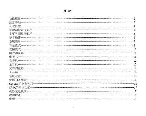
目录功能概述 (2)注意事项 (2)认识机型 (4)按键功能定义说明 (5)主要界面显示说明 (5)基本操作 (8)系统菜单 (8)音乐模式 (8)视频模式 (10)图片浏览器 (10)电子书 (11)收音机 (12)录音机 (13)文件浏览器 (14)工具箱 (15)系统设置 (15)使用USB磁盘 (16)MINISD扩充卡使用 (16)AV OUT输出功能 (17)机器充电说明 (17)故障解决 (18)申明 (19)为了您能尽快轻松自如地操作索爱数码播放器,我们随机配备了内容详尽的用户手册,从中您可以获取有关的产品介绍,使用方法等方面的知识,在您开始使用MP5数码播放器之前,请仔细阅读我们随机提供的所有资料,以便您能正确使用产品。
功能概述●高清晰真彩TFT彩屏显示,支持480×272分辨率●支持MP3、WMA、WAV、FLAC等音乐格式●支持MPEG-4(AVI)、RMVB、RM 720P高清视频格式不需转换,有些格式需转换。
●支持插卡功能MININ SD卡128M/256M/512M/1GB/2GB/4GB 等●支持高清晰JPEG和GIF格式图片浏览●数码录音,A-B复读功能●节能设置:亮度可自由调节,定时关机时间●支持3D音效设置,均衡音效。
●多种循环风格:单曲循环、全部循环、单曲播放、顺序播放、随机播放●支持多国语言●支持桌面背景设置,桌面模式设置,桌面时间设置等各性化设置。
●支持游戏功能●USB2.0高速传输●支持电子书阅读,书签功能●具备世界时间查询日历功能时间显示●AV OUT输出功能:LCD、AV_PAL、AV_NTSC●移动U盘功能,支持固件升级●支持操作系统:Windows98/SE/ME/2K/XP●使用温度:-5至40摄氏度注意事项本手册含有重要的安全措施和正确使用产品的信息,为避免事故发生,请在使用该产品之前仔细阅读该手册。
●请不要将产品放在高温度、潮湿或灰尘多的地方使用,以免影响产品寿命●避免摔落或强烈碰撞产品,不要让TFT屏遭到猛烈震动,否则可能导致TFT屏损坏或显示不正常●请选择合适的音量,使用耳机不宜过大音量,若感到耳鸣,请调小音量或停止使用●在下列情况下请充电:A、电池电量图标显示空时B、系统自动关机,再次开机后很快关机C、操作按键没有反应●本播放器采用的是高容量锂电池,可重复充电使用. 在前几次充电必须充够8小时,并且每次用完电量再进行充电,以保证电池的使用寿命。
魅族17使用说明书

魅族17使用说明书运营商与网络•运营商支持全网通5G (运营商支持向下兼容)•网络模式双卡双待•SIM卡类型Nano-SIM卡+Nano-SIM卡•WiFi支持Wi-Fi 6•蓝牙支持蓝牙5.1•手机类型面部识别,拍照手机,全面屏,后置四摄,骁龙865,自拍神器,大屏手机,大容量电池,快充手机,指纹识别,支持NFC,5G手机机身信息•机身结构直板•手机颜色松深入墨,十七度灰,AG梦幻独角兽•手机尺寸160×77.2×8.5mm屏幕信息系统与硬件相机拍照影音娱乐定位与传感器基本功能包装配件保修信息便捷小窗用途多多Flyme系统的小窗使用体验长期以来受到了网友的一致好评,在Flyme 8上小窗功能也得到了升级。
很多用户在观看视频时,都经历过杂事打扰被迫切换到其它APP中从而导致观影体验“断断续续”的情况,而Flyme 8的视频小窗功能便可以很好地帮助用户解决魅族17上用户可以在手机桌面或者是其它应用上使用悬浮的视频小窗,还可以在全屏播放视频时通过小窗功能使用其它APP进行办公、聊天、阅读等操作。
借助Flyme 8的小窗功能,用户还可以实现在不同场景下进行快速回复。
当接到消息推送时,用户只需要点开通知框的小窗打开功能,聊天界面就会以小窗的形式悬浮在当前界面上,回复完消息,点击小窗外的区域即可关闭小窗。
此外,用户还可以使用手势从屏幕的下角向内滑动唤醒小窗功能,从而不需要关闭当前的应用便可以使用其他软件。
通知小窗回复游戏模式告别烦恼除了便捷的小窗功能之外,魅族17的游戏模式也同样可以在游戏的情况下为用户带来便捷的游戏内操作体验。
首先为了避免在游戏中弹出的系统输入法占据大半个屏幕的问题,魅族17的游戏模式内置了游戏悬浮小键盘功能,有了这个功能用户就可以随心在游戏内完成输入,无需担心过大的键盘面积遮挡游戏画面的问题。
游戏悬浮小键盘其次,为了解决不同游戏中按键振感适配的问题,用户可以通过游戏助手功能中的游戏振感设置手动设置振感的虚拟映射位置。
IMX8-7-F;IMX8-7;中文规格书,Datasheet资料

• Epitaxial Planar Die Construction • Complementary PNP Type Available (IMT4) • Small Surface Mount Package • Lead Free/RoHS Compliant (Note 3) • "Green" Device, Note 4 and 5
IEBO
⎯
⎯
0.5
μA VEB = 4.0V
hFE
180
⎯
820
⎯ IC = 2.0mA, VCE = 6.0V
VCE(SAT)
⎯
⎯
0.5
V IC = 10mA, IB = 1.0mA
fT
⎯
140
⎯
MHz VCE = 12V, IC = 2.0mA, f = 100MHz
Notes:
1. Device mounted on FR-5 PCB 1.0 x 0.75 x 0.062 inch pad layout as shown on Diodes Inc. suggested pad layout AP02001, which can be found on our website at /datasheets/ap02001.pdf. 200mW per element must not be exceeded.
Symbol VCBO VCEO VEBO IC Pd RθJA
Tj, TSTG
Value 120 120 5.0 50 300 417
-55 to +150
Unit V V V mA
mW °C/W
°C
Electrical Characteristics @TA = 25°C unless otherwise specified
IMX芯片系列分类——按像素尺寸
IMX芯片系列分类——按像素尺寸说明:感光面积越大,夜晚拍照效果越好。
第一阵营:imx600、imx650,1.6-2μmIMX600,尺寸为1/1.73′,4000万像素,等效1.6μm,以Quad Bayer排列,用于华为P20 pro。
IMX650,尺寸为1/1.7′,4000万像素,等效2.0μm第二阵营:imx378、imx380,1.55μmIMX378,有效像素1220万像素,尺寸为1/2.3英寸(7.81mm),单个像素尺寸为1.55μm。
用于谷歌的Pixel和小米5s。
imx380是imx378的小改款,1.55μm,用于华为P20手机和魅族15。
第三阵营:imx260、imx333、imx362、imx363,1.4μmimx260,1200万像素,单位像素尺寸1.4μm。
用于三星的S7 imx362,1200万像素,单位像素尺寸1.4μm,支持全像素双核对焦技术,对焦速度快。
用于魅蓝note6、魅蓝E3、红米note6、努比亚Z17、MOTO G5p等。
imx333,1200万像素,单位像素尺寸1.4μm,定制版,用于三星S8imx363,1200万像素,单位像素尺寸1.4μm,定制版,用于小米mix2s、Vivo Nex第四阵营:imx386(imx286)、imx400、imx519,1.22-1.25μm。
imx286,感光元件面积1/2.9英寸,单个像素面积1.25μm。
用于华为P9imx315,单个像素面积1.22μm,用于苹果6Simx386,1200万像素,单个像素1.25μm,传感器尺寸为1/2.8英寸。
支持PDAF,采用索尼的DTI像素隔离技术,可以有效减少相邻像素之间的窜扰。
最早应用的是魅族的MX6,后来用于坚果PRO2、小米note3、小米6。
imx400,1/2.3英寸,单个像素为1.22μm,但是索尼在CMOS 封装了一块DRAM,支持1080p960帧慢镜头拍摄。
LM1117 中文PDF资料
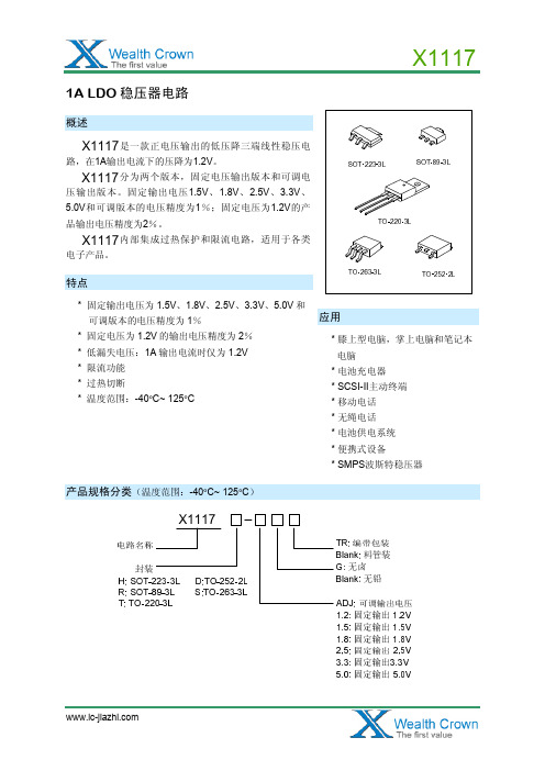
VOUT 22 F
R2 VOUT=VREF x (1+R2/R1)+IADJ x R2
图 2. 典型可调输出电压
注:以上线路及参数仅供参考,实际的应用电路请在充分的实测基础上设定参数。
输出电压变化(%)
典型电气特性曲线
温度稳定性
负载瞬态反应(VOUT=5 V)
可调管脚电流 ( A)
参数符号测试条件最小值典型值最大值单位x1117adj基准电压vrefiout10mavinvout2vtj25c123812501262v10maiout1a14vvinvout10v122512501270x111712iout10mvin32vtj25c1176121224v10maiout1a30vvin10v1152121248x111715iout10mvin35vtj25c148515001515v10maiout1a30vvin10v147015001530x111718iout10mavin38vtj25c178218001818v0iout1a32vvin10v176418001836输出电压voutx111725iout10mavin45vtj25c247525002525v0iout1a39vvin10v245025002550x111733iout10mavin5vtj25c326733003333v0iout1a475vvin10v323533003365x111750iout10mavin7vtj25c49505000505v0iout1a65vvin12v49005000510输出电压温度稳定性tsout03vinminvin12v线性调整rline37mvvoutfixedadjiout10ma负载调整rload10maiout1avoutfixedadj612mviout100ma100120漏失电压vdropiout500ma105125viout1a110130静态电流iq425vvin65v510mafripple120hzvinvout3v纹波抑制比psrr6075dbvripple1vpp可调管脚电流iadj60120a可调管脚电流变化0iout1a14vvinvout10v025a温保点tsd150c限流点ilimit121415ax1117参数符号测试条件最小值典型值最大值单位温度稳定性05长期稳定性tamb125c1000hrs0
IMX系列选型对照表

i.MX 6SoloLite
ARM Cortex-A9 1 GHz 32 KB/32 KB L1, 256 KB L2 128 KB x32 LP-DDR2, DDR3/LV-DDR3 SXGA+ (1400 x 1050) No SW Only
i.MX53
ARM Cortex™-A8 1.2 GHz 32 KB/32 KB L1, 256 KB L2 128 KB DDR2, DDR3, LP-DDR2, LV-DDR2, NOR, SLC/MLC, Managed NAND UXGA (1600 x 1200) No HD720p Video Encode, HD1080p Decode Open GL ES 2.0 and OpenVG 1.1 2 5 3/3 HS USB 2.0 OTG, 3x HS USB 2.0 Host 2
Open VG 1 3 2/3 HS OTG, HS Host 2
No No 6 4/2 HS Host/Device, HS Host 2
No 1 5 3/3 HS OTG, HS Host 2
Please note: The product data sheet and reference manual are your best source for the most current and detailed technical data on the i.MX processor you prefer. For documentation on i.MX applications processors, visit /imx. Share ideas, design tips and meet other i.MX fans at .
第三部分CQI-17 教材-IPC 20130703 V2
验收条件 对各级产品均分有四级验收条件:
目标条件 可接受条件 缺陷条件 过程警示条件
验收条件
目标条件
定义:指近乎完美/首选的情况,然而这是一种理想而非总 能达到的情形,且对于保证组件在使用环境下的可靠性并 非必要的情形。
可接受条件
定义:组件不必完美,但要在使用环境下保持完整性和可 靠性的特征。
设计标准
成品文件
IPC-D-325
成品标准 可接受标准
返工/返修
IPC-J-STD-001 IPC-A-610
IPC-7711/7721
焊接的电气和电子组件的要求 电子组件的可接受性 提供进行敷形涂覆层和元器件的拆除及 更换,阻焊膜维修,层压板材料,导线 和镀覆孔的修改与维修的操作程序文件
锡焊系统审核 (SSA )----参考文件(IPC-A-610E)
验收条件
制程警示(非缺陷)条件
定义:没有影响到产品的外形、装配和功能(3F)的情况。 指存在一些不符合要求的特征但并不影响产品的形状、安 装和功能。 由材料、设计、操作人员或设备等原因引起。 单一原因的过程警示项目不需要处置,受影响的产品可“ 照样使用”。
验收条件
制程警示条件 (续)
锡焊系统审核 (SSA )----参考文件(IPC-A-610E)
IPC-A-610E“电子组件可接受性标准”版本介绍: 1983年8月: 1990年3月: 1994年12月: 2000年1月: 2005年2月: IPC-A-610 IPC-A-610A IPC-A-610B IPC-A-610C IPC-A-610D
元器件的安装
3、元器件安装——连接器
缺陷:1,2,3 级
由于连接器的倾斜,与之匹配的连接 器无法插入。 元器件的高度不符合标准的规定。 定位销没有完全插入/扣住PCB板 元器件的引脚伸出焊盘的长度不符合 要求 注:连接器需要满足外形、装配和功 能的要求。如果需要,可采用连接器 间匹配试验作最终接收条件。
IMX芯片系列分类——按发布序号

IMX芯⽚系列分类——按发布序号术语 前照式传感器:传统CMOS在感光元件的感光层前⾯有⼀排⾦属电路,光线要先通过⾦属排线电路才能到达感光层,这就影响了透光率,甚⾄造成像素⼲扰。
背照式传感器:背照式是相对于传统CMOS前照式⽽⾔的。
⽽背照式传感器将前照式的⾦属电路层移到了感光层后⾯,从⽽提⾼光线利⽤率。
堆栈式传感器:堆栈式传感器是对背照式结构的改进。
背照式中的感光层原来也是有电路的并且和后⾯的电路层相连,堆栈式就是将感光层的像素部分进⼀步独⽴出来,将其中的电路层挪⾄下⽅替代原有的⽀持基板,进⼀步提⾼了感光层的利⽤率。
PDAF相位对焦:是指感光元件上预留出⼀些遮蔽像素点,专门⽤来进⾏相位检测,通过像素之间的距离及其变化等来决定对焦的偏移值从⽽实现⽐传统反差对焦更准确更快速的对焦。
双像素对焦:是基于PDAF改进的技术,将每个⼦像素⼀分为⼆,每个像素⼀半⽤来接收被摄物体图像信息,⼀半⽤来侦测负责对焦的相位差像素,从⽽让所有像素点都可以侦测相位差对焦,从⽽解决PDAF暗光或夜拍对焦慢的问题。
四像素合⼀:在传统的RGBG拜⽿像素阵列上进⾏改进,将四个同⾊的RGBG像素排列在⼀起,形成⼀个⼤的RGBG像素阵列,从⽽提⾼感光能⼒。
⼿机上的CMOS感光元件,有索尼的IMX系列,还有豪威(OV)、三星(ISOCELL)等。
索尼Exmor传感器产品系列。
在智能⼿机上使⽤的主要为Exmor R和Exmor RS系列。
Exmor R为背照式传感器系列,是索尼在2008年6⽉发布的。
⽬前它们在智能⼿机上已经⼏乎销声匿迹。
⼀、Exmor R系列 IMX179 是索尼的第三代背照式技术摄像头,感光⾯积为1/3.2英⼨,每像素单位尺⼨为1.4um,800万。
IMX179在暗光环境下表现明显。
IMX179的帧率达到了30fps。
IMX145,iPhone量⾝定制影像传感器 IMX377,4032 x 3024,12.2 MP,7.81 mm (1/2.3"),1.55 µm⼆、Exmor RS系列1、Exmor RS IMX1系 2012年8⽉,索尼推出了IMX135、IMX134和ISX014三款堆栈式图像传感器。
鳞状细胞癌抗原、糖类抗原125检测在宫颈鳞癌中的应用价值

鳞状细胞癌抗原、糖类抗原125检测在宫颈鳞癌中的应用价值杨丽;高艳章;李秋菊;杨伟;赵三红【摘要】Objective To study the clinical value of squamous cell carcinoma associated antigcn(SCC) and CA125 in the diagnosis and monitoring of squamous cell carcinoma of the cervix. Methods The samples of peripheral venous blood from 85 patients with cervix squamousccll carcinoma, 60 patients with cervical intracpithclial ncoplasia(CIN) and 45 healthy women were collected. Then the scrum SCC was measured by IMX,and CA125 was measured by Roche El70. Results The levels and positive rates of SCC were significantly higher than those in the other groups(P<0. 05) , but the levels and positive rates of CA125 were not variable. With the increasing of FIGO stage,the levels and positive rates of SCC and the levels of CA125 increased significantly (P<0. 05). The post-treatment SCC level was significantly lower than that of pretrcatment (P<0. 05). But CA125 level was not variable. Both SCC and CA125 did not change with the pathological grades significantly. Conclusion SCC contributes to the diagnosis of cervix squamous cell carcinoma and observing therapeutic efficacy. CA125 is not so helpful for cervix squamous cell carcinoma in the diagnosis and observing therapeutic efficacy. The combined determination can improve the diagnostic sensitivity.%目的探讨肿瘤标志物鳞状细胞癌抗原(SCC)与糖类抗原125(CA125)检测在宫颈鳞状细胞癌中的应用价值.方法对经临床病理确诊的85例宫颈鳞状细胞癌患者、60例宫颈上皮内瘤样病变(CIN)患者以及45例健康妇女,采用雅培微粒子免疫分析仪IMX和罗氏电化学发光分析仪E170分别检测血清SCC和CA125数值,比较分析二者改变的临床意义.结果与正常对照组及CIN组相比,宫颈鳞癌组治疗前血清SCC水平及阳性率均较高 (P<0.05);而CA125在三组间无统计学差异(P>0.05).在国际妇产科联盟(Federation International of Gynecology and Obstetrics,FIGO)分期中,SCC水平及阳性率随分期上升而增加(P<0.05);而CA125仅浓度改变有统计学差异(P<0.05).SCC和CA125在不同病理分级中均无显著改变(P>0.05).宫颈鳞癌患者治疗前后的血清SCC改变,差异有统计学意义(P<0.05);而血清CA125无统计学差异(P>0.05).结论 SCC测定可作为宫颈鳞癌诊断的辅助指标,用于病情进展、治疗效果的监测.而CA125在宫颈鳞癌诊疗中的意义不大,二者联合检测可以提高对宫颈鳞癌诊断的敏感性.【期刊名称】《中国实验诊断学》【年(卷),期】2013(017)002【总页数】3页(P350-352)【关键词】鳞状细胞癌抗原;CA125;宫颈鳞癌;肿瘤标志物【作者】杨丽;高艳章;李秋菊;杨伟;赵三红【作者单位】云南省肿瘤医院·昆明医科大学第三附属医院,检验科,云南,昆明650118【正文语种】中文【中图分类】R737.33宫颈癌是常见的妇科恶性肿瘤之一,从目前的病理诊断来看,宫颈鳞状细胞癌占了宫颈癌的95%。
