87941-08;87943-08;中文规格书,Datasheet资料
744314047;中文规格书,Datasheet资料

Bezeichnung :description :Marking = part numberEigenschaften /properties Lerrlaufinduktivität/initial inductance Nenn-Induktivität /33% Umgebungstemperatur / temperature:+20°CWE-Superflux ME08-01-01ME 06-09-27NameDatum / dateArbeitstemperatur / operating temperature: -40°C - +150°C Metra HIT 27I für/for R DCFreigabe erteilt / general release:Kunde / customerF Werkstoffe & Zulassungen / material & approvals :Würth Elektronik..................................................................................G Eigenschaften / general specifications :not exceed 150°C under worst case operating conditions.It is recommended that the temperature of the part does coating:blackHP 34401 A & Fluke 54II für/for I DC; Luftfeuchtigkeit / humidity:WAYNE KERR 3260B für/for L 0; I SAT Elektrische Eigenschaften / electrical properties :Umgebungstemp. / ambient temperature: -40°C - +100°C Basismaterial / base material:Draht / wire: AIEIW-200 D Prüfgeräte / test equipment :http://www.we-online.deDatum / date..................................................................................Unterschrift / signatureKontrolliert / approvedWürth Elektronik eiSos GmbH & Co. KGD-74638 Waldenburg · Max-Eyth-Strasse 1 - 3 · Germany · Telefon (+49) (0) 7942 - 945 - 0 · Telefax (+49) (0) 7942 - 945 - 400Geprüft / checked .................................................................................................POWER-CHOKE WE-HCIE Testbedingungen / test conditions :Änderung / modificationVersion 1Version 2Bezeichnung :description :H Induktivitätskurve / Inductance curve :ME08-01-01ME 06-09-27NameDatum / dateD-74638 Waldenburg · Max-Eyth-Strasse 1 - 3 · Germany · Telefon (+49) (0) 7942 - 945 - 0 · Telefax (+49) (0) 7942 - 945 - 400http://www.we-online.deGeprüft / checked Kontrolliert / approvedÄnderung / modificationWürth Elektronik eiSos GmbH & Co. KGVersion 2..............................................................................................................................................Version 1Datum / dateUnterschrift / signature Würth Elektronik....................................................................................................................................................................Freigabe erteilt / general release:Kunde / customerPOWER-CHOKE WE-HCIDATUM / DATE : 2008-01-01Bezeichnung :description :I Temperaturanstieg / Temperature rise curve :ME08-01-01ME 06-09-27NameDatum / dateWürth ElektronikVersion 2..........................................................................................................................................Freigabe erteilt / general release:Kunde / customerDatum / dateUnterschrift / signature...............................................................................................................................................................Version 1D-74638 Waldenburg · Max-Eyth-Strasse 1 - 3 · Germany · Telefon (+49) (0) 7942 - 945 - 0 · Telefax (+49) (0) 7942 - 945 - 400http://www.we-online.deGeprüft / checked Kontrolliert / approvedÄnderung / modificationWürth Elektronik eiSos GmbH & Co. KGBezeichnung :description :a 330,0± 2,0mmb 21,0± 0,8mmc 13,00± 0,5mmd 100,0± 1,5mmME08-01-01ME 06-09-27NameDatum / dateD-74638 Waldenburg · Max-Eyth-Strasse 1 - 3 · Germany · Telefon (+49) (0) 7942 - 945 - 0 · Telefax (+49) (0) 7942 - 945 - 400Geprüft / checked Kontrolliert / approvedÄnderung / modificationWürth Elektronik eiSos GmbH & Co. KGVersion 2................................................................................................................................................Version 1Datum / dateUnterschrift / signature Würth Elektronik....................................................................................................................................................................Freigabe erteilt / general release:Kunde / customerRollenspezifikation / Reel specification:SPEICHERDROSSEL WE-HCI POWER-CHOKE WE-HCIThe Force for tearing off cover tape is 20 to 70 grams in arrow direction150°feeding directionThis electronic component has been designed and developed for usage in general electronic equipment. Before incorporating this component into any equipment where higher safety and reliability is especially required or if there is the possibility of direct damage or injury to human body, for example in the range of aerospace, aviation, nuclear control, submarine, transportation, (automotive control, train control, ship control), transportation signal, disaster prevention, medical, public information network etc, Würth Elektronik eiSos GmbH must be informed before the design-in stage. In addition, sufficient reliability evaluation checks for safety must be performed on every electronic component which is used in electrical circuits that require high safety and reliability functions or performance.分销商库存信息: WURTH-ELECTRONICS 744314047。
37640;37641;37642;37643;37644;中文规格书,Datasheet资料
Thickness is +/- 1/16” *Dimensions are nominal; thickness is +/- 1/16”
Special and die cut sizes available on a quotation basis. Made in America
PROTEKTIVE PAK 13520 MONTE VISTA AVENUE, CHINO, CA 91710 PHONE (909) 627-2578, FAX (909) 363-7331
Description:
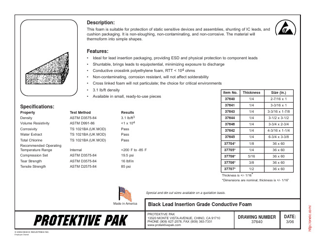
This foam is suitable for protection of static sensitive devices and assemblies, shunting of IC leads, and cushion packaging. It is non-sloughing, non-contaminating, and non-corrosive. The material will thermoform into simple shapes.
© 2006 DESCO INDUSTRIES INC.
Employee Owned
DRAWING NUMBER 37640
DATE: 3/06
/
Black Lead Insertion Grade Conductive Foam
分销商库存信息:
DESCO 37640 37643 37646 37706 37641 37644 37704 37707 37642 37645 37705 37708
Item No. 37640 37641 Test Method ASTM D3575-84 ASTM D991-86 TS 1021BA (UK MOD) TS 1021BA (UK MOD) TS 1021BA (UK MOD) Internal ASTM D3575-84 ASTM D3575-84 ASTM D2575-84 Results 3.1 lb/ft3 <1 x 10⁴ Pass Pass Pass +200°F to -85°F 19.5 psi 16 lbf/in 85 psi 37643 37644 37646 37642 37645 37704* 37705* 37708* 37706* 37707* Thickness 1/4 1/4 1/4 1/4 1/4 1/4 1/4 1/8 1/4 5/16 3/8 1/2 Size (in.) 2-7/16 x 1 3-3/16 x 1 3-3/16 x 1-7/8 3-1/2 x 3-1/2 3-3/4 x 2-3/4 4-3/16 x 1-1/4 6-3/4 x 3-3/8 36 x 60 36 x 60 36 x 60 36 x 60 36 x 60
8718;8738;8739;8719;8720;中文规格书,Datasheet资料
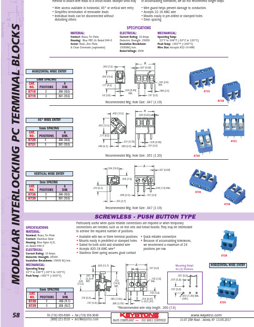
Tel (718) 956-8900•Fax (718) 956-9040(800) 221-5510•kec@31-07 20th Road –Astoria,NY 11105-2017RoHS COMPLIANT ~ISO 9001 CERTIFIED®5mm SPACINGCAT.A NO.POSITIONSDIM.87282.459 (11.7)87293.656 (16.7)5mm SPACINGCAT.ANO.POSITIONS DIM.87202.394 (10.0)87213.591 (15.0)5mm SPACING CAT.A NO.POSITIONSDIM.87182.394 (10.0)87193.591 (15.0)M O D U L A R I N T E R L O C K I N G P C T E R M I N A L B L O C K S58SCREWLESS - PUSH BUTTON TYPESPECIFICATIONS MATERIAL:Terminal:Brass,Tin Plate Contact:Stainless Steel Housing:Blue Nylon 6/6,UL Rated 94V-0ELECTRICAL:Current Rating: 10 Amps Dielectric Strength:2500VInsulation Breakdown:1500V AC/min.MECHANICAL:Operating Temp:22°F to 248°F (-30°C to 120°C)Peak Temp:+392°F (+200°C)Particularly useful when quick reliable connections are required or when temporaryconnections are needed,such as on test sets and bread boards.They may be interlocked to achieve the required number of positions .•Available with two or three terminal positions •Mounts easily in predrilled or stamped holes •Suited for both solid and stranded wire •Accepts #20-18 AWG wire*•Stainless Steel spring assures good contact•Quick reliable connection•Because of accumulating tolerances,we recommend a maximum of 24 positions per row.*Recommended wire strip length: .300 (7.6)Recommended Mtg.Hole Size: .047 (1.19)Recommended Mtg.Hole Size: .051 (1.30)SPECIFICATIONS .098 [2.5].027 [0.69].300 [7.6]A.197 [5.0]50 [3.8].177 [4.5].394 [10.0].100 [2.6]DIA..039 [0.99]DIA..024 [0.61].248 [6.3].177 [4.5].492 [12.5].098 [2.5].197 [5.0]A.492 [12.5].031 [0.79].039 [0.99]Mounting Detail for (3) Postions.197 [5.0].197 [5.0].197 [5.0].051 [1.30] DIA.(TYP.).500 [12.7].091[2.3]REF..753[19.2]REF..142 [3.6].520[13.2].065 [1.65].197 [5.0].118 [3.0].197 [5.0]A.086 [2.18].142 [3.6]DIA..016 [0.41]x .032 [.81]MATERIAL:Contact: Brass,Tin PlateHousing: Blue PBT,UL Rated 94V-0 Screw:Steel,Zinc Plate& Clear Chromate (captivated)ELECTRICAL:Current Rating:16 Amps Dielectric Strength: 2500V Insulation Breakdown:1500VAC/min.Rated Voltage:250VMECHANICAL:Operating Temp:22°F to 248°F (-30°C to 120°C)Peak Temp:+393°F (+200°C)Wire Size:Accepts #22-14 AWGHORIZONTAL WIRE ENTRY5mm SPACINGCAT.A NO.POSITIONSDIM.87382.394 (10.0)87393.591 (15.0)Recommended Mtg.Hole Size: .047 (1.19)method to attach wire leads to a circuit board.Multiple units may of accumulating tolerances,we do not recommend longer strips.•Wire access available in horizontal,45°or vertical wire entry •Simplifies termination of removable leads •Individual leads can be disconnected withoutdisturbing others •Wire guard helps prevent damage to conductors •Accepts 22-16 AWG wire•Mounts easily in pre-drilled or stamped holes •5mm spacing.197 [5.0]A.300 [7.6].027 [0.69].098 [2.5].210 [5.3].105 [2.7].394 [10.0].039 [1.0] DIA.87198718872187208739873887288729HORIZONTAL WIRE ENTRY 45°WIRE ENTRY VERTICAL WIRE ENTRY分销商库存信息:KEYSTONE-ELECTRONICS871887388739 871987208728 87218729。
FDU8796中文资料
2
元器件交易网
FDD8796/FDU8796 N-Channel PowerTrench® MOSFET
Typical Characteristics TJ = 25°C unless otherwise noted
ID, DRAIN CURRENT (A)
ID, DRAIN CURRENT (A)
70
PULSE DURATION = 80µs 60 DUTY CYCLE = 0.5%MAX
50
TJ = 175oC
40
30 TJ = 25oC
20
10
TJ = -55oC
0
0
1
2
3
4
VGS, GATE TO SOURCE VOLTAGE (V)
Figure 5. Transfer Characteristics
AD FREE I
General Description
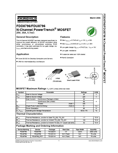
This N-Channel MOSFET has been designed specifically to improve the overall efficiency of DC/DC converters using either synchronous or conventional switching PWM controllers. It has been optimized for low gate charge, low rDS(on) and fast switching speed.
Parameter
VDS
Drain to Source Voltage
VGS
Gate to Source Voltage
Drain Current -Continuous (Package Limited)
0878321014;中文规格书,Datasheet资料
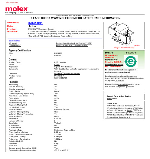
This document was generated on 08/16/2012PLEASE CHECK FOR LATEST PART INFORMATIONPart Number:87832-1014Status:ActiveOverview:Milli-Grid™ Connector SystemDescription:2.00mm Pitch Milli-Grid™ Header, Surface Mount, Vertical, Shrouded, Lead-Free, 10Circuits, 0.38µm Gold (Au) Plating, without Locking Window, Center Polarization Slot,Cap, without PCB Locator, Embossed Tape on ReelDocuments:3D ModelProduct Specification PS-87831-027 (PDF)Drawing (PDF)RoHS Certificate of Compliance (PDF)Agency CertificationCSA LR19980ULE29179GeneralProduct Family PCB Headers Series87832Application Signal, Wire-to-BoardComments With Cap|Contact Molex for application in automotive industryOverviewMilli-Grid™ Connector System Product Name Milli-Grid™UPC822350245791PhysicalBreakawayNo Circuits (Loaded)10Circuits (maximum)10Color - ResinBlack Durability (mating cycles max)100First Mate / Last Break No Flammability94V-0Glow-Wire Compliant No Guide to Mating Part No Keying to Mating Part Yes Lock to Mating Part YesMaterial - MetalPhosphor Bronze Material - Plating MatingGold Material - Plating Termination Tin Material - Resin Nylon Net Weight0.670/g Number of Rows 2Orientation Vertical PCB Locator No PCB Retention NonePackaging TypeEmbossed Tape on Reel Pitch - Mating Interface2.00mm Pitch - Termination Interface 2.00mm Plating min - Mating0.381µm Plating min - Termination 1.905µm Polarized to PCB No Shrouded Fully StackableNo Surface Mount Compatible (SMC)YesTemperature Range - Operating-55°C to +105°CSeriesimage - Reference onlyEU RoHSChina RoHSELV and RoHS Compliant REACH SVHCContains SVHC: No Low-Halogen Status Not Low-HalogenNeed more information on product environmental compliance?Email productcompliance@For a multiple part number RoHS Certificate of Compliance, click herePlease visit the Contact Us section for any non-product compliance questions.Search Parts in this Series 87832SeriesMates With50394 Wire-to-Board Terminals, 51110Wire-to-Board Crimp Housing, 87568 Wire-to-Board IDT Housings, 79107 Board-to-Board Top Entry Through Hole Receptacle,79108 Board-to-Board FFC/FPC Top Entry Through Hole Receptacle, LTermination Interface: Style Through Hole and Surface MountElectricalCurrent - Maximum per Contact2AVoltage - Maximum125VSolder Process DataDuration at Max. Process Temperature (seconds)10Lead-free Process Capability Reflow Capable (SMT only)Max. Cycles at Max. Process Temperature1Process Temperature max. C260Material InfoReference - Drawing NumbersProduct Specification PS-87831-027Sales Drawing SD-87832-008This document was generated on 08/16/2012PLEASE CHECK FOR LATEST PART INFORMATION分销商库存信息: MOLEX 0878321014。
TLC1549CP;TLC1549IP;TLC1549CD;TLC1549ID;TLC1549CDR;中文规格书,Datasheet资料

TLC1549MFK
Please be aware that an important notice concerning availability, standard warranty, and use in critical applications of Texas Instruments semiconductor products and disclaimers thereto appears at the end of this data sheet.
Copyright © 1995, Texas Instruments Incorporated
description
The TLC1549C is characterized for operation from 0°C to 70°C. The TLC1549I is characterized for operation from – 40°C to 85°C. The TLC1549M is characterized for operation over the full military temperature range of – 55°C to 125°C.
PRODUCTION DATA information is current as of publication date. Products conform to specifications per the terms of Texas Instruments standard warranty. Production processing does not necessarily include testing of all parameters.
Sample and Hold
SN74AHC1G86_08中文资料
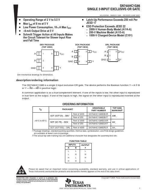
PACKAGING INFORMATIONOrderable Device Status(1)PackageType PackageDrawingPins PackageQtyEco Plan(2)Lead/Ball Finish MSL Peak Temp(3)SN74AHC1G86DBVG4ACTIVE SOT-23DBV5TBD Call TI Call TISN74AHC1G86DBVR ACTIVE SOT-23DBV53000Green(RoHS&no Sb/Br)CU NIPDAU Level-1-260C-UNLIMSN74AHC1G86DBVRE4ACTIVE SOT-23DBV53000Green(RoHS&no Sb/Br)CU NIPDAU Level-1-260C-UNLIMSN74AHC1G86DBVRG4ACTIVE SOT-23DBV53000Green(RoHS&no Sb/Br)CU NIPDAU Level-1-260C-UNLIMSN74AHC1G86DBVT ACTIVE SOT-23DBV5250Green(RoHS&no Sb/Br)CU NIPDAU Level-1-260C-UNLIMSN74AHC1G86DBVTE4ACTIVE SOT-23DBV5250Green(RoHS&no Sb/Br)CU NIPDAU Level-1-260C-UNLIMSN74AHC1G86DBVTG4ACTIVE SOT-23DBV5250Green(RoHS&no Sb/Br)CU NIPDAU Level-1-260C-UNLIMSN74AHC1G86DCKR ACTIVE SC70DCK53000Green(RoHS&no Sb/Br)CU NIPDAU Level-1-260C-UNLIMSN74AHC1G86DCKRE4ACTIVE SC70DCK53000Green(RoHS&no Sb/Br)CU NIPDAU Level-1-260C-UNLIMSN74AHC1G86DCKRG4ACTIVE SC70DCK53000Green(RoHS&no Sb/Br)CU NIPDAU Level-1-260C-UNLIMSN74AHC1G86DCKT ACTIVE SC70DCK5250Green(RoHS&no Sb/Br)CU NIPDAU Level-1-260C-UNLIMSN74AHC1G86DCKTE4ACTIVE SC70DCK5250Green(RoHS&no Sb/Br)CU NIPDAU Level-1-260C-UNLIMSN74AHC1G86DCKTG4ACTIVE SC70DCK5250Green(RoHS&no Sb/Br)CU NIPDAU Level-1-260C-UNLIMSN74AHC1G86DRLR ACTIVE SOT DRL54000Green(RoHS&no Sb/Br)CU NIPDAU Level-1-260C-UNLIMSN74AHC1G86DRLRG4ACTIVE SOT DRL54000Green(RoHS&no Sb/Br)CU NIPDAU Level-1-260C-UNLIM(1)The marketing status values are defined as follows:ACTIVE:Product device recommended for new designs.LIFEBUY:TI has announced that the device will be discontinued,and a lifetime-buy period is in effect.NRND:Not recommended for new designs.Device is in production to support existing customers,but TI does not recommend using this part in a new design.PREVIEW:Device has been announced but is not in production.Samples may or may not be available.OBSOLETE:TI has discontinued the production of the device.(2)Eco Plan-The planned eco-friendly classification:Pb-Free(RoHS),Pb-Free(RoHS Exempt),or Green(RoHS&no Sb/Br)-please check /productcontent for the latest availability information and additional product content details.TBD:The Pb-Free/Green conversion plan has not been defined.Pb-Free(RoHS):TI's terms"Lead-Free"or"Pb-Free"mean semiconductor products that are compatible with the current RoHS requirements for all6substances,including the requirement that lead not exceed0.1%by weight in homogeneous materials.Where designed to be soldered at high temperatures,TI Pb-Free products are suitable for use in specified lead-free processes.Pb-Free(RoHS Exempt):This component has a RoHS exemption for either1)lead-based flip-chip solder bumps used between the die and package,or2)lead-based die adhesive used between the die and leadframe.The component is otherwise considered Pb-Free(RoHS compatible)as defined above.Green(RoHS&no Sb/Br):TI defines"Green"to mean Pb-Free(RoHS compatible),and free of Bromine(Br)and Antimony(Sb)based flame retardants(Br or Sb do not exceed0.1%by weight in homogeneous material)(3)MSL,Peak Temp.--The Moisture Sensitivity Level rating according to the JEDEC industry standard classifications,and peak solder temperature.Important Information and Disclaimer:The information provided on this page represents TI's knowledge and belief as of the date that it is provided.TI bases its knowledge and belief on information provided by third parties,and makes no representation or warranty as to the accuracy of such information.Efforts are underway to better integrate information from third parties.TI has taken and continues to take reasonable steps to provide representative and accurate information but may not have conducted destructive testing or chemical analysis on incoming materials and chemicals.TI and TI suppliers consider certain information to be proprietary,and thus CAS numbers and other limited information may not be available for release.In no event shall TI's liability arising out of such information exceed the total purchase price of the TI part(s)at issue in this document sold by TI to Customer on an annual basis.TAPE AND REEL INFORMATION*All dimensions are nominalDevicePackage Type Package Drawing Pins SPQReel Diameter (mm)Reel Width W1(mm)A0(mm)B0(mm)K0(mm)P1(mm)W (mm)Pin1Quadrant SN74AHC1G86DBVR SOT-23DBV 53000178.09.0 3.23 3.17 1.37 4.08.0Q3SN74AHC1G86DBVR SOT-23DBV 53000180.09.2 3.23 3.17 1.37 4.08.0Q3SN74AHC1G86DBVT SOT-23DBV 5250180.09.2 3.23 3.17 1.37 4.08.0Q3SN74AHC1G86DCKR SC70DCK 53000180.09.2 2.24 2.34 1.22 4.08.0Q3SN74AHC1G86DCKR SC70DCK 53000178.09.0 2.4 2.5 1.2 4.08.0Q3SN74AHC1G86DCKT SC70DCK 5250178.09.0 2.4 2.5 1.2 4.08.0Q3SN74AHC1G86DCKT SC70DCK 5250180.09.2 2.24 2.34 1.22 4.08.0Q3SN74AHC1G86DRLRSOTDRL54000180.09.21.781.780.694.08.0Q3*All dimensions are nominalDevice Package Type Package Drawing Pins SPQ Length(mm)Width(mm)Height(mm) SN74AHC1G86DBVR SOT-23DBV53000180.0180.018.0 SN74AHC1G86DBVR SOT-23DBV53000202.0201.028.0 SN74AHC1G86DBVT SOT-23DBV5250202.0201.028.0 SN74AHC1G86DCKR SC70DCK53000202.0201.028.0 SN74AHC1G86DCKR SC70DCK53000180.0180.018.0 SN74AHC1G86DCKT SC70DCK5250180.0180.018.0 SN74AHC1G86DCKT SC70DCK5250202.0201.028.0 SN74AHC1G86DRLR SOT DRL54000202.0201.028.0IMPORTANT NOTICETexas Instruments Incorporated and its subsidiaries(TI)reserve the right to make corrections,modifications,enhancements,improvements, and other changes to its products and services at any time and to discontinue any product or service without notice.Customers should obtain the latest relevant information before placing orders and should verify that such information is current and complete.All products are sold subject to TI’s terms and conditions of sale supplied at the time of order acknowledgment.TI warrants performance of its hardware products to the specifications applicable at the time of sale in accordance with TI’s standard warranty.Testing and other quality control techniques are used to the extent TI deems necessary to support this warranty.Except where mandated by government requirements,testing of all parameters of each product is not necessarily performed.TI assumes no liability for applications assistance or customer product design.Customers are responsible for their products and applications using TI components.To minimize the risks associated with customer products and applications,customers should provide adequate design and operating safeguards.TI does not warrant or represent that any license,either express or implied,is granted under any TI patent right,copyright,mask work right, or other TI intellectual property right relating to any combination,machine,or process in which TI products or services are rmation published by TI regarding third-party products or services does not constitute a license from TI to use such products or services or a warranty or endorsement e of such information may require a license from a third party under the patents or other intellectual property of the third party,or a license from TI under the patents or other intellectual property of TI.Reproduction of TI information in TI data books or data sheets is permissible only if reproduction is without alteration and is accompanied by all associated warranties,conditions,limitations,and notices.Reproduction of this information with alteration is an unfair and deceptive business practice.TI is not responsible or liable for such altered rmation of third parties may be subject to additional restrictions.Resale of TI products or services with statements different from or beyond the parameters stated by TI for that product or service voids all express and any implied warranties for the associated TI product or service and is an unfair and deceptive business practice.TI is not responsible or liable for any such statements.TI products are not authorized for use in safety-critical applications(such as life support)where a failure of the TI product would reasonably be expected to cause severe personal injury or death,unless officers of the parties have executed an agreement specifically governing such use.Buyers represent that they have all necessary expertise in the safety and regulatory ramifications of their applications,and acknowledge and agree that they are solely responsible for all legal,regulatory and safety-related requirements concerning their products and any use of TI products in such safety-critical applications,notwithstanding any applications-related information or support that may be provided by TI.Further,Buyers must fully indemnify TI and its representatives against any damages arising out of the use of TI products in such safety-critical applications.TI products are neither designed nor intended for use in military/aerospace applications or environments unless the TI products are specifically designated by TI as military-grade or"enhanced plastic."Only products designated by TI as military-grade meet military specifications.Buyers acknowledge and agree that any such use of TI products which TI has not designated as military-grade is solely at the Buyer's risk,and that they are solely responsible for compliance with all legal and regulatory requirements in connection with such use. TI products are neither designed nor intended for use in automotive applications or environments unless the specific TI products are designated by TI as compliant with ISO/TS16949requirements.Buyers acknowledge and agree that,if they use any non-designated products in automotive applications,TI will not be responsible for any failure to meet such requirements.Following are URLs where you can obtain information on other Texas Instruments products and application solutions:Products ApplicationsAmplifiers AudioData Converters AutomotiveDSP BroadbandClocks and Timers Digital ControlInterface MedicalLogic MilitaryPower Mgmt Optical NetworkingMicrocontrollers SecurityRFID TelephonyRF/IF and ZigBee®Solutions Video&ImagingWirelessMailing Address:Texas Instruments,Post Office Box655303,Dallas,Texas75265Copyright©2008,Texas Instruments Incorporated。
742863160;中文规格书,Datasheet资料

3.1 3.0 2.02012-06-272012-03-292009-08-13SStSStSMuSStSMu-Würth Elektronik eiSos GmbH & Co. KGEMC & Inductive SolutionsMax-Eyth-Str. 174638 WaldenburgGermanyTel. +49 (0) 79 42 945 - 0A Dimensions: [mm]F Typical Impedance Characteristics:Test Equipment: E4991A or equivalentF Derating Curve:H1: Classification Reflow Profile for SMT components:H2: Classification Reflow ProfilesProfile FeaturePreheat- Temperature Min (T smin ) - Temperature Max (T smax ) - Time (t s ) from (T smin to T smax )Ramp-up rate (T L to T P )Liquidous temperature (T L )Time (t L ) maintained above T L Peak package body temperature (T p )Time within 5°C of actual peak temperature (t p )Ramp-down rate (T P to T L )Time 25°C to peak temperature Pb-Free Assembly 150°C 200°C60-180 seconds 3°C/ second max.217°C60-150 seconds See Table H320-30 seconds 6°C/ second max.8 minutes max.refer to IPC/JEDEC J-STD-020DH3: Package Classification Reflow TemperaturePB-Free Assembly PB-Free Assembly PB-Free Assembly Package Thickness< 1.6 mm 1.6 - 2.5 mm ≥ 2.5 mmVolume mm³<350260°C 260°C 250°CVolume mm³350 - 2000260°C 250°C 245°CVolume mm³>2000260°C 245°C 245°Crefer to IPC/JEDEC J-STD-020DH Soldering Specifications:I Cautions and Warnings:The following conditions apply to all goods within the product series of WE-CBF HFof Würth Elektronik eiSos GmbH & Co. KG:General:All recommendations according to the general technical specifications of the data-sheet have to be complied with.The disposal and operation of the product within ambient conditions which probably alloy or harm the component surface has to be avoided.If the product is potted in customer applications, the potting material might shrink during and after hardening. Accordingly to this the product is exposed to the pressure of the potting material with the effect that the ferrite body and termination is possibly damaged by this pressure and so the electrical as well as the mechanical characteristics are endanger to be affected. After the potting material is cured, the ferrite body and termination of the product have to be checked if any reduced electrical or mechanical functions or destructions have occurred.The responsibility for the applicability of customer specific products and use in a particular customer design is always within the authority of the customer. All technical specifications for standard products do also apply for customer specific products.Washing varnish agent that is used during the production to clean the application might damage or change the characteristics of the plating. The washing varnish agent could have a negative effect on the long term function of the product.Direct mechanical impact to the product shall be prevented as the ferrite material of the ferrite body could flake or in the worst case it could break.Product specific:Follow all instructions mentioned in the datasheet, especially:•The solder profile has to be complied with according to the technical reflow soldering specification, otherwise no warranty will be sustai-ned.• Wave soldering is only allowed after evaluation and approval.•All products are supposed to be used before the end of the period of 12 months based on the product date-code, if not a 100% solderabi-lity can´t be warranted.•Violation of the technical product specifications such as exceeding the nominal rated current will result in the loss of warranty.1. General Customer ResponsibilitySome goods within the product range of Würth Elektronik eiSos GmbH & Co. KG contain statements regarding general suitability for certain application areas. These statements about suitability are based on our knowledge and experience of typical requirements concerning the are-as, serve as general guidance and cannot be estimated as binding statements about the suitability for a customer application. The responsibi-lity for the applicability and use in a particular customer design is always solely within the authority of the customer. Due to this fact it is up to the customer to evaluate, where appropriate to investigate and decide whether the device with the specific product characteristics described in the product specification is valid and suitable for the respective customer application or not.2. Customer Responsibility related to Specific, in particular Safety-Relevant ApplicationsIt has to be clearly pointed out that the possibility of a malfunction of electronic components or failure before the end of the usual lifetime can-not be completely eliminated in the current state of the art, even if the products are operated within the range of the specifications.In certain customer applications requiring a very high level of safety and especially in customer applications in which the malfunction or failure of an electronic component could endanger human life or health it must be ensured by most advanced technological aid of suitable design of the customer application that no injury or damage is caused to third parties in the event of malfunction or failure of an electronic component.3. Best Care and AttentionAny product-specific notes, warnings and cautions must be strictly observed.4. Customer Support for Product SpecificationsSome products within the product range may contain substances which are subject to restrictions in certain jurisdictions in order to serve spe-cific technical requirements. Necessary information is available on request. In this case the field sales engineer or the internal sales person in charge should be contacted who will be happy to support in this matter.5. Product R&DDue to constant product improvement product specifications may change from time to time. As a standard reporting procedure of the Product Change Notification (PCN) according to the JEDEC-Standard inform about minor and major changes. In case of further queries regarding the PCN, the field sales engineer or the internal sales person in charge should be contacted. The basic responsibility of the customer as per Secti-on 1 and 2 remains unaffected.6. Product Life CycleDue to technical progress and economical evaluation we also reserve the right to discontinue production and delivery of products. As a stan-dard reporting procedure of the Product Termination Notification (PTN) according to the JEDEC-Standard we will inform at an early stage about inevitable product discontinuance. According to this we cannot guarantee that all products within our product range will always be available. Therefore it needs to be verified with the field sales engineer or the internal sales person in charge about the current product availability ex-pectancy before or when the product for application design-in disposal is considered.The approach named above does not apply in the case of individual agreements deviating from the foregoing for customer-specific products.7. Property RightsAll the rights for contractual products produced by Würth Elektronik eiSos GmbH & Co. KG on the basis of ideas, development contracts as well as models or templates that are subject to copyright, patent or commercial protection supplied to the customer will remain with Würth Elektronik eiSos GmbH & Co. KG.8. General Terms and ConditionsUnless otherwise agreed in individual contracts, all orders are subject to the current version of the “General Terms and Conditions of Würth Elektronik eiSos Group”, last version available at .J Important Notes:The following conditions apply to all goods within the product range of Würth Elektronik eiSos GmbH & Co. KG:分销商库存信息: WURTH-ELECTRONICS 742863160。
MX879RTR;MX879R;中文规格书,Datasheet资料

Features•Eight (8) Outputs Rated at 60V , -120mA •Open-Drain, Pull-Up Driver Configuration •6V to 60V Driver Supply Range •2.7V to 5.5V Logic Supply Range•3-Wire Serial Interface plus Chip Select •Captures Serial & Parallel Input Data •Outputs Can Be Paralleled •28-Lead QFN PackageApplications•White Goods •A TE•Industrial EquipmentDescriptionThe MX879 is an 8-channel, high voltage switch with 8-bit parallel or serial input control. The MX879 connects directly to a microprocessor through a standard 3-wire serial interface. The open-drain,pull-up output configuration can drive up to 60 volts at -120mA. Outputs can be paralleled for increased drive current up to a device total of 600mA source.The MX879 is designed to operate over a temperature range of -40°C to +85°C, and is available in a 28-lead QFN Package.Ordering InformationFunctional Block DiagramPartDescriptionMX879R QFN-28 (73/T ube)MX879RTRQFN-28 T ape & Reel (2500/Reel)1. Specifications . . . . . . . . . . . . . . . . . . . . . . . . . . . . . . . . . . . . . . . . . . . . . . . . . . . . . . . . . . . . . . . . . . . . . . . . . . . . . . . . . . . . . . . . . . . . . . 31.1 Package Pinout . . . . . . . . . . . . . . . . . . . . . . . . . . . . . . . . . . . . . . . . . . . . . . . . . . . . . . . . . . . . . . . . . . . . . . . . . . . . . . . . . . . . . . . . . 31.2 Pin Description. . . . . . . . . . . . . . . . . . . . . . . . . . . . . . . . . . . . . . . . . . . . . . . . . . . . . . . . . . . . . . . . . . . . . . . . . . . . . . . . . . . . . . . . . . 31.3 Absolute Maximum Ratings. . . . . . . . . . . . . . . . . . . . . . . . . . . . . . . . . . . . . . . . . . . . . . . . . . . . . . . . . . . . . . . . . . . . . . . . . . . . . . . . 41.4 DC Electrical Characteristics. . . . . . . . . . . . . . . . . . . . . . . . . . . . . . . . . . . . . . . . . . . . . . . . . . . . . . . . . . . . . . . . . . . . . . . . . . . . . . . 41.5 Dynamic Electrical Characteristics. . . . . . . . . . . . . . . . . . . . . . . . . . . . . . . . . . . . . . . . . . . . . . . . . . . . . . . . . . . . . . . . . . . . . . . . . . . 51.6 Serial Timing . . . . . . . . . . . . . . . . . . . . . . . . . . . . . . . . . . . . . . . . . . . . . . . . . . . . . . . . . . . . . . . . . . . . . . . . . . . . . . . . . . . . . . . . . . . 61.7 Parallel Timing. . . . . . . . . . . . . . . . . . . . . . . . . . . . . . . . . . . . . . . . . . . . . . . . . . . . . . . . . . . . . . . . . . . . . . . . . . . . . . . . . . . . . . . . . . 62. Functional Description . . . . . . . . . . . . . . . . . . . . . . . . . . . . . . . . . . . . . . . . . . . . . . . . . . . . . . . . . . . . . . . . . . . . . . . . . . . . . . . . . . . . . . . 73. Application Examples. . . . . . . . . . . . . . . . . . . . . . . . . . . . . . . . . . . . . . . . . . . . . . . . . . . . . . . . . . . . . . . . . . . . . . . . . . . . . . . . . . . . . . . . 83.1 Parallel In / Parallel Out Application. . . . . . . . . . . . . . . . . . . . . . . . . . . . . . . . . . . . . . . . . . . . . . . . . . . . . . . . . . . . . . . . . . . . . . . . . . 83.2 Serial Cascade Application . . . . . . . . . . . . . . . . . . . . . . . . . . . . . . . . . . . . . . . . . . . . . . . . . . . . . . . . . . . . . . . . . . . . . . . . . . . . . . . . 83.3 Control System Application . . . . . . . . . . . . . . . . . . . . . . . . . . . . . . . . . . . . . . . . . . . . . . . . . . . . . . . . . . . . . . . . . . . . . . . . . . . . . . . . 94. Manufacturing Information. . . . . . . . . . . . . . . . . . . . . . . . . . . . . . . . . . . . . . . . . . . . . . . . . . . . . . . . . . . . . . . . . . . . . . . . . . . . . . . . . . . 104.1 Moisture Sensitivity . . . . . . . . . . . . . . . . . . . . . . . . . . . . . . . . . . . . . . . . . . . . . . . . . . . . . . . . . . . . . . . . . . . . . . . . . . . . . . . . . . . . . 104.2 ESD Sensitivity . . . . . . . . . . . . . . . . . . . . . . . . . . . . . . . . . . . . . . . . . . . . . . . . . . . . . . . . . . . . . . . . . . . . . . . . . . . . . . . . . . . . . . . . 104.3 Reflow Profile. . . . . . . . . . . . . . . . . . . . . . . . . . . . . . . . . . . . . . . . . . . . . . . . . . . . . . . . . . . . . . . . . . . . . . . . . . . . . . . . . . . . . . . . . . 104.4 Mechanical Dimensions. . . . . . . . . . . . . . . . . . . . . . . . . . . . . . . . . . . . . . . . . . . . . . . . . . . . . . . . . . . . . . . . . . . . . . . . . . . . . . . . . . 111Specifications1.1 Package Pinout1.2 Pin DescriptionPin#Name Description1OUT7Parallel Output 2N/C No Connection 3GND Ground4V PWR High Voltage Supply (6V to 60V)5N/C No Connection6V CC Logic Supply (2.7V to 5.5V)7SDO Serial Data Output 8IN7Parallel Input 9IN6Parallel Input 10IN5Parallel Input 11IN4Parallel Input 12IN3Parallel Input 13IN2Parallel Input 14IN1Parallel Input 15IN0Parallel Input 16SCK Serial Clock17V PWR High Voltage Supply (6V to 60V)18SDI Serial Data Input 19CS*Chip Select (Active Low)20OE Output Enable 21GND Ground 22OUT0Parallel Output 23OUT1Parallel Output 24OUT2Parallel Output 25OUT3Parallel Output 26OUT4Parallel Output 27OUT5Parallel Output 28OUT6Parallel Output1.3 Absolute Maximum RatingsVoltages with respect to GND=0V .Absolute maximum electrical ratings are at 25°CAbsolute Maximum Ratings are stress ratings. Stresses in excess of these ratings can cause permanent damage to the device. Functional operation of the device at these or any other conditions beyond those indicated in the operational sections of this data sheet is not implied.Exposure of the device to the absolute maximum ratings for an extended period may degrade the device and affect its reliability.ESD Warning: ESD (electrostatic discharge) sensitive device. Although the MX879 features proprietary ESD protectioncircuitry, permanent damage may be sustained if subjected to high energy electrostatic discharges. Proper ESD precautions are recommended to avoid performance degradation or loss of functionality.1.4 DC Electrical CharacteristicsV CC =5V , V PWR =42V , T A =25°C, unless otherwise specified.Notes:T o avoid unwanted output during VPWR application and system initialization, keep OE at a logic low until CS* has completed one cycle.Thermal Resistance is measured in still air with the device soldered to a 6 square inch board without a ground plane. Applications may require derating of the specified maximum currents to avoid exceeding the maximum operation junction temperature.ParameterSymbolMinMaxUnitsVPWR Supply Voltage V PWR -60V Logic Supply Voltage V CC -6V Input Pin Voltage VIN -6V Continuous Output Current OUT0 - OUT7I OUTn --150mA Operating Junction T emperature T J -150°C Thermal Resistance (Junction to Ambient)R θJA 110 T ypical °C/W Operating T emperature T A -4085°C Storage T emperatureT STG-55150°CParameterConditionsMinimumTypicalMaximumUnitsLogic Supply Voltage - 2.7- 5.5V Logic Supply Current f SCK =5MHz -50-μA Quiescent Logic Supply Current f SCK =0--1μA V PWR Voltage -6-60V V PWR Current T otal of all Outputs --600mA Quiescent V PWR Current V PWR =42V , No Load -0.75-mA High Level Input Voltage IN0-IN7, SCK, SDI, OE, CS*V CC -0.5--V Low Level Input Voltage ---0.5V Input Leakage Current ---1μA SDO T ri-State Leakage Current CS*=Logic High --1μA OUT0-OUT7 Current Any One Output, Source---120mA OUT0-OUT7 ON Resistance V PWR =42V -7-ΩOUT0-OUT7 T ri-State Leakage CurrentOE=Logic Low--1μA1.5 Dynamic Electrical CharacteristicsV CC=5V, V PWR=42V, T A=25°C, unless otherwise specified.Parameter Conditions Symbol Minimum Typical Maximum Units SCK Period--100-DC ns SCK High Time--40--ns SCK Low Time--40--ns CS* High Time-tCSwh50--ns CS* Falling to SCK Rising Setup Time tCSs150--ns CS* Low Time SCK Low (Parallel Input Mode)tCSwl150--ns INx to CS Falling (SETUP TIME)-tINs15--ns INx to CS Falling (HOLD TIME)-tINh30--ns SDI to SCK Rising (SETUP TIME)-tSDIs20--ns SDI to SCK Rising (HOLD TIME)-tSDIh25--nsSCK Falling to to SDO Data Valid-tSDO-10-ns CS* Rising to SDO High Z-tSDOz-12-ns CS* Rising to OUTx Rising T o 50%, C(OUTx)=1000pF tOUT r-680-ns OUTx Rise Time From 10% to 90%, C(OUTx)=1000pF--110-ns OE Rising to OUTx Rising T o 90%--580-ns OE Rising to OUTx Falling T o 90%--390-nsOE Falling to OUTx High Z T o 10%, OUTx High--130-nsT o 10%, OUTx Low--90-ns1.6 Serial Timing1.7 Parallel Timing2Functional DescriptionThe MX879 is an 8-channel high-voltage driver with 8-bit input control. The MX879 interfaces to a microprocessor through a standard 3-wire serial interface and an active-low chip select, or can be used in a parallel-in, parallel-out configuration.Parallel data is transferred to the I/O register of the MX879 through the parallel input pins, IN0 throughIN7, on the falling edge of the chip select pin, CS*. When CS* is in a logic-low state, serial data can be transferred to the I/O register through the serial input pin, SDI, and from the I/O register through the serial output pin, SDO. Parallel or serial input data is transferred from the I/O register to the latch and high voltage output drivers, OUT0 through OUT7, on the positive edge of CS*. This data remains latched until the next positive edge of CS*.The 8-bit I/O shift register is clocked by the serial clock pin, SCK. Serial data presented at the SDI pin is transferred to the shift register on the positive edge of SCK. Data shifts out of the register through the SDO pin on the negative edge of SCK. SDI and SCK are ignored, and SDO transitions to a high impedance condition when CS* is at a logic high state.Serial data is received by the MX879 through the SDI pin. This data is accepted on the rising edge of SCK. A specific output is programmed to a logic-high state if SDI is at a logic-high state during the rising edge of SCK. Conversely, a specific output is programmed to a logic-low state if SDI is at a logic-low state during the rising edge of SCK. Outputs transition to their programmed states on the positive edge of CS* if the output enable pin, OE, is in a logic-high state.The MSB input data (IN7) is presented at the serial output pin, SDO, on the falling edge of CS*. Input data from IN6 through IN0 is sequentially presented at SDO on negative SCK transitions if CS* remains in a logic-low state. If CS* is at a logic-low state beyond 8 cycles of SCK, SDI data that has propagated through the I/O register will then be presented at SDO. The SDO pin transitions to a high-impedance state when CS* is in a logic-high state, thus allowing multiple serial peripherals to share the microprocessor data pin.Figure 1. Serial Data Transfer ExampleDevices may be serially cascaded by connecting SDO to SDI of the next device. Pins SCK and CS* are common to all devices in serial cascade. Forn-cascaded devices the CS* should remain low for 8n cycles of SCK.An output enable pin, OE, enables the driver outputs OUT0 through OUT7 when logic-high. A logic-low level on OE forces the OUT0 through OUT7 outputs to a high-impedance state.The MX879 can also operate as a parallel-in, parallel-out level shifter and driver. SCK must remain at a logic-low state when operating in this mode. Parallel input data presented to IN0 through IN7 is captured on the falling edge of CS*. This data is transferred to OUT0 through OUT7 on the rising edge of CS*, and remains latched until the next rising edge of CS*.3Application Examples3.1 Parallel In / Parallel Out Application3.2 Serial Cascade Application3.3 Control System Application4Manufacturing Information4.1 Moisture SensitivityAll plastic encapsulated semiconductor packages are susceptible to moisture ingression. Clare classified all of its plastic encapsulated devices for moisture sensitivity according to the latest version of the joint industry standard, IPC/JEDEC J-STD-020, in force at the time of product evaluation. We test all of our products to the maximum conditions set forth in the standard, and guarantee proper operation of ourdevices when handled according to the limitations and information in that standard as well as to any limitations set forth in the information or standards referenced below.Failure to adhere to the warnings or limitations as established by the listed specifications could result in reduced product performance, reduction of operable life, and/or reduction of overall reliability.This product carries a Moisture Sensitivity Level (MSL) rating as shown below, and should be handled according to the requirements of the latest version of the joint industry standard IPC/JEDEC J-STD-033.4.2 ESD SensitivityThis product is ESD Sensitive , and should be handled according to the industry standard JESD-625.4.3 Reflow ProfileThis product has a maximum body temperature and time rating as shown below. All other guidelines of J-STD-020 must be observed.Device Moisture Sensitivity Level (MSL) RatingMX879RMSL 3Device Maximum Temperature x TimeMX879R260°C for 30 seconds分销商库存信息:IXYSMX879RTR MX879R。
CS8441YN8;中文规格书,Datasheet资料
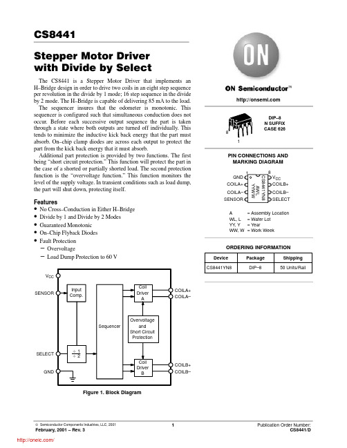
CS8441Stepper Motor Driver with Divide by SelectThe CS8441 is a Stepper Motor Driver that implements an H–Bridge design in order to drive two coils in an eight step sequence per revolution in the divide by 1 mode; 16 step sequence in the divide by 2 mode. The H–Bridge is capable of delivering 85 mA to the load.The sequencer insures that the odometer is monotonic. This sequencer is configured such that simultaneous conduction does not occur. Before each successive output sequence the part is taken through a state where both outputs are turned off individually. This tends to minimize the inductive kick back energy that the part must absorb. On–chip clamp diodes are across each output to protect the part from the kick back energy that it must absorb.Additional part protection is provided by two functions. The first being “short circuit protection.” This function will protect the part in the case of a shorted or partially shorted load. The second protection function is the “overvoltage function.” This function monitors the level of the supply voltage. In transient conditions such as load dump,the part will shut down, protecting itself.Features•No Cross–Conduction in Either H–Bridge •Divide by 1 and Divide by 2 Modes •Guaranteed Monotonic •On–Chip Flyback Diodes •Fault Protection –Overvoltage–Load Dump Protection to 60 VSENSORV CCGNDSELECTCOILA+COILA–COILB+COILB–Figure 1. Block DiagramA = Assembly Location WL, L = Wafer Lot YY , Y = YearWW, W= Work WeekPIN CONNECTIONS AND MARKING DIAGRAMDIP–8N SUFFIX CASE 62618CS8441YN8AWL YYWWV CC COILB+COILB–SELECTGND COILA+COILA–SENSOR 1Device Package Shipping ORDERING INFORMATIONCS8441YN8DIP–850 Units/RailABSOLUTE MAXIMUM RATINGS*2.10 second maximum.*The maximum package power dissipation must be observed.ELECTRICAL CHARACTERISTICS (–40°C ≤ T A≤ 125°C, 6.5 V ≤ V CC≤ 15.5 V; unless otherwise stated. All voltageshall be referenced to GND unless otherwise noted. Overvoltage shutdown of coils occurs when V CC > 16 V.)Characteristic Test Conditions Min Typ Max UnitCoil Output Drivers3.Voltage across the coils shall be measured at the specific voltages, but shall also be within linearly interpolated limits.ELECTRICAL CHARACTERISTICS (continued) (–40°C ≤ T A≤ 125°C, 6.5 V ≤ V CC≤ 15.5 V; unless otherwise stated. All voltage shall be referenced to GND unless otherwise noted. Overvoltage shutdown of coils occurs when V> 16 V.)Short Circuit ProtectionPACKAGE PIN DESCRIPTIONCIRCUIT OPERATIONSPEED SENSOR INPUTSENSOR is a PNP comparator input which accepts a sine wave or a square wave input. This input is protected from excursions above V CC as well as any below ground, as long as the current is limited to 1.5 mA. It has an active clamp set to zero volts to prevent negative input voltages from disrupting normal operation. The sensor input can withstand 150 V DC as long as the input current is limited to 1.5 mA max. using a series resistor of 100 kΩ.COIL DRIVER OUTPUTS Simultaneously energizing the source and sink on either leg is not permitted, i.e. Q1 & Q2 or Q3 & Q4 cannot be energized simultaneously.Circuit function is not affected by inductive transients due to coil loads as specified in the Transition States section. The transition states occur as indicated in Table 1 without any intermediate states permitted.The polarity definition for the coil driver outputs is as follows:DIVIDER SELECT INPUTThe speed sensor input frequency is divided by one or divided by two by connecting the divider select input, (Pin 5) as follows:Logic 0 = divide by 2.Logic 1 = divide by 1.Figure 2. Coil Driver Output01234567012345670State #SSICoil ACoil BFigure 3. Divide by 1 (8 Step Mode), SELECT = 1State #SSICoil ACoil BFigure 4. Divide by 2 (16 Step Mode), SELECT = 0IGNCOIL A210 ±12 ΩCOIL B210 ±12 ΩFigure 5. Odometer Application DiagramPACKAGE DIMENSIONSDIP–8N SUFFIX CASE 626–05ISSUE LNOTES:1.DIMENSION L TO CENTER OF LEAD WHEN FORMED PARALLEL.2.PACKAGE CONTOUR OPTIONAL (ROUND OR SQUARE CORNERS).3.DIMENSIONING AND TOLERANCING PER ANSI Y14.5M, 1982.DIM MIN MAX MIN MAX INCHESMILLIMETERS A 9.4010.160.3700.400B 6.10 6.600.2400.260C 3.94 4.450.1550.175D 0.380.510.0150.020F 1.02 1.780.0400.070G 2.54 BSC 0.100 BSC H 0.76 1.270.0300.050J 0.200.300.0080.012K 2.92 3.430.1150.135L 7.62 BSC 0.300 BSC M ---10 ---10 N0.76 1.010.0300.040__PACKAGE THERMAL DATANotesh ON Semiconductor and are trademarks of Semiconductor Components Industries, LLC (SCILLC). SCILLC reserves the right to make changeswithout further notice to any products herein. SCILLC makes no warranty, representation or guarantee regarding the suitability of its products for any particularpurpose, nor does SCILLC assume any liability arising out of the application or use of any product or circuit, and specifically disclaims any and all liability,including without limitation special, consequential or incidental damages. “Typical” parameters which may be provided in SCILLC data sheets and/orspecifications can and do vary in different applications and actual performance may vary over time. All operating parameters, including “Typicals” must bevalidated for each customer application by customer’s technical experts. SCILLC does not convey any license under its patent rights nor the rights of others.SCILLC products are not designed, intended, or authorized for use as components in systems intended for surgical implant into the body, or other applicationsintended to support or sustain life, or for any other application in which the failure of the SCILLC product could create a situation where personal injury ordeath may occur. Should Buyer purchase or use SCILLC products for any such unintended or unauthorized application, Buyer shall indemnify and holdSCILLC and its officers, employees, subsidiaries, affiliates, and distributors harmless against all claims, costs, damages, and expenses, and reasonableattorney fees arising out of, directly or indirectly, any claim of personal injury or death associated with such unintended or unauthorized use, even if such claimalleges that SCILLC was negligent regarding the design or manufacture of the part. SCILLC is an Equal Opportunity/Affirmative Action Employer.PUBLICATION ORDERING INFORMATIONCENTRAL/SOUTH AMERICA:Spanish Phone:303–308–7143 (Mon–Fri 8:00am to 5:00pm MST)Email:ONlit–spanish@ASIA/PACIFIC: LDC for ON Semiconductor – Asia SupportPhone:303–675–2121 (Tue–Fri 9:00am to 1:00pm, Hong Kong Time)Toll Free from Hong Kong & Singapore:001–800–4422–3781Email: ONlit–asia@JAPAN: ON Semiconductor, Japan Customer Focus Center4–32–1 Nishi–Gotanda, Shinagawa–ku, Tokyo, Japan 141–0031Phone: 81–3–5740–2745Email: r14525@分销商库存信息: ONSEMICS8441YN8。
NJD2873T4G;中文规格书,Datasheet资料

NJD2873T4G,NJVNJD2873T4GPower TransistorsNPN Silicon DPAK For Surface Mount ApplicationsDesigned for high−gain audio amplifier applications.Features•High DC Current Gain −h FE = 120 (Min) @ I C = 500 mA= 40 (Min) @ I C = 2 A•Low Collector−Emitter Saturation V oltage −V CE(sat) = 0.3 Vdc (Max) @ I C = 1 A•High Current−Gain − Bandwidth Product −f T = 65 MHz (Min) @ I C = 100 mA•Epoxy Meets UL 94 V−0 @ 0.125 in•ESD Ratings:♦Human Body Model, 3B > 8000 V♦Machine Model, C > 400 V•NJV Prefix for Automotive and Other Applications Requiring Unique Site and Control Change Requirements; AEC−Q101 Qualified and PPAP Capable•These are Pb−Free PackagesMAXIMUM RATINGSRating Symbol Value Unit Collector−Base Voltage V CB50Vdc Collector−Emitter Voltage V CEO50Vdc Emitter−Base Voltage V EB5VdcCollector Current Continuous Peak I C23AdcBase Current I B0.4AdcTotal Device Dissipation @ T C = 25°C Derate above 25°C P D150.1WW/°CTotal Device Dissipation @ T A = 25°C* Derate above 25°C P D1.680.011WW/°COperating and Storage JunctionTemperature RangeT J, T stg−65 to +175°CStresses exceeding Maximum Ratings may damage the device. Maximum Ratings are stress ratings only. Functional operation above the Recommended Operating Conditions is not implied. Extended exposure to stresses above the Recommended Operating Conditions may affect device reliability.Device Package Shipping†ORDERING INFORMATIONSILICONPOWER TRANSISTORS2 AMPERES50 VOLTS15 WATTS†For information on tape and reel specifications, including part orientation and tape sizes, please refer to our Tape and Reel Packaging Specification Brochure, BRD8011/D.MARKING DIAGRAMA= Assembly LocationY= YearWW= Work WeekG= Pb−Free DeviceDPAKCASE 369CSTYLE 1AYWWJ2873GNJD2873T4G DPAK(Pb−Free)2,500Units / Reel NJVNJD2873T4G DPAK(Pb−Free)2,500Units / Reel11BASE3EMITTERCOLLECTOR2,424THERMAL CHARACTERISTICSCharacteristic Symbol Max UnitThermal ResistanceJunction−to−CaseJunction−to−Ambient (Note 1)R q JCR q JA1089.3°C/W1.These ratings are applicable when surface mounted on the minimum pad sizes recommended.ELECTRICAL CHARACTERISTICS (T C = 25°C unless otherwise noted)Characteristic Symbol Min Max Unit OFF CHARACTERISTICSCollector−Emitter Sustaining Voltage (Note 2) (I C = 10 mAdc, I B = 0)V CEO(sus)50−VdcCollector Cutoff Current (V CB = 50 Vdc, I E = 0)I CBO−100nAdcEmitter Cutoff Current (V BE = 5 Vdc, I C = 0)I EBO−100nAdc ON CHARACTERISTICSDC Current Gain (Note 2)(I C = 0.5 A, V CE = 2 V)(I C = 2 Adc, V CE = 2 Vdc)(I C = 0.75 Adc, V CE = 1.6 Vdc, −40°C ≤ T J≤ 150°C)h FE1204080360−360−Collector−Emitter Saturation Voltage (Note 2) (I C = 1 A, I B = 0.05 A)V CE(sat)−0.3VdcBase−Emitter Saturation Voltage (Note 2) (I C = 1 A, I B = 0.05 Adc)V BE(sat)− 1.2VdcBase−Emitter On Voltage (Note 2)(I C = 1 Adc, V CE = 2 Vdc)(I C = 0.75 Adc, V CE = 1.6 Vdc, −40°C ≤ T J≤ 150°C)V BE(on)−−1.20.95VdcDYNAMIC CHARACTERISTICSCurrent−Gain − Bandwidth Product (Note 3)(I C = 100 mAdc, V CE = 10 Vdc, f test = 10 MHz)f T65−MHzOutput Capacitance(V CB = 10 Vdc, I E = 0, f = 0.1 MHz)C ob−80pF2.Pulse Test: Pulse Width = 300 m s, Duty Cycle [ 2%.3.f T = ⎪h fe⎪• f test.TYPICAL CHARACTERISTICS0.010.1110I C , COLLECTOR CURRENT (AMPS)V C E (s a t ), C O L L E C T O R −E M I T T E R S A T U R A T I O N V O L T A G E (V )I C , COLLECTOR CURRENT (AMPS)V B E (s a t ), B A S E −E M I T T E R S A T U R A T I O N V O L T A G E (V )10010000.010.1110I C , COLLECTOR CURRENT (AMPS)h F E , D C C U R R E N T G A I N102525Figure 1. Power DeratingT, TEMPERATURE (°C)50751001251501510520P D , P O W E R D I S S I P A T I O N (W A T T S )Figure 2. DC Current Gain Figure 3. Collector −Emitter Saturation VoltageFigure 4. Base −Emitter Saturation Voltage Figure 5. Base −Emitter VoltageI C , COLLECTOR CURRENT (AMPS)V B E (o n ), B A S E −E M I T T E R V O L T A G E (V )1.21.00.80.60.40.21.10.90.70.50.3175200Figure 6. Saturation RegionI B , BASE CURRENT (mA)V C E (s a t ), C O L L E C T O R −E M I T T E R S A T U R A T I O N V O L T A G E (V )1.00.010.11100.80.60.40.2010010000.11101001000100101Figure 7. CapacitanceV R , REVERSE VOLTAGE (V)C , C A P A C I T A N C E (p F )Figure 8. Saturation RegionI C , COLLECTOR CURRENT (mA)f t a u , C U R R E N T G A I N B A N D W I D T H P R O D U C T (M H z )1001101001000100100001101001000100101Figure 9. CapacitanceV CE , COLLECTOR EMITTER VOLTAGE (V)I C , C O L L E C T O R C U R R E N T10000t, TIME (ms)r (t ), T R A N S I E N T T H E R M A L R E S I S T A N C E (N O R M A L I Z E D )Figure 10. Thermal ResponsePACKAGE DIMENSIONSDPAK CASE 369C ISSUE DSTYLE 1:PIN 1.BASE2.COLLECTOR3.EMITTER4.COLLECTORǒmm ǓSCALE 3:1*For additional information on our Pb −Free strategy and solderingdetails, please download the ON Semiconductor Soldering and Mounting Techniques Reference Manual, SOLDERRM/D.SOLDERING FOOTPRINT*DIM MIN MAX MIN MAX MILLIMETERSINCHES D 0.2350.245 5.97 6.22E 0.2500.265 6.35 6.73A 0.0860.094 2.18 2.38b 0.0250.0350.630.89c20.0180.0240.460.61b20.0300.0450.76 1.14c 0.0180.0240.460.61e 0.090 BSC 2.29 BSC b30.1800.215 4.57 5.46L4−−−0.040−−− 1.01L 0.0550.070 1.40 1.78L30.0350.0500.89 1.27Z0.155−−−3.93−−−NOTES:1.DIMENSIONING AND TOLERANCING PER ASME Y14.5M, 1994.2.CONTROLLING DIMENSION: INCHES.3.THERMAL PAD CONTOUR OPTIONAL WITHIN DI-MENSIONS b3, L3 and Z.4.DIMENSIONS D AND E DO NOT INCLUDE MOLD FLASH, PROTRUSIONS, OR BURRS. MOLDFLASH, PROTRUSIONS, OR GATE BURRS SHALL NOT EXCEED 0.006 INCHES PER SIDE.5.DIMENSIONS D AND E ARE DETERMINED AT THE OUTERMOST EXTREMES OF THE PLASTIC BODY .6.DATUMS A AND B ARE DETERMINED AT DATUM PLANE H.H 0.3700.4109.4010.41A10.0000.0050.000.13L10.108 REF 2.74 REF L20.020 BSC 0.51 BSC DETAIL AROTATED 90 CW 5ON Semiconductor and are registered trademarks of Semiconductor Components Industries, LLC (SCILLC). SCILLC owns the rights to a number of patents, trademarks,copyrights, trade secrets, and other intellectual property. A listing of SCILLC’s product/patent coverage may be accessed at /site/pdf/Patent −Marking.pdf. SCILLC reserves the right to make changes without further notice to any products herein. SCILLC makes no warranty, representation or guarantee regarding the suitability of its products for any particular purpose, nor does SCILLC assume any liability arising out of the application or use of any product or circuit, and specifically disclaims any and all liability, including without limitation special, consequential or incidental damages. “Typical” parameters which may be provided in SCILLC data sheets and/or specifications can and do vary in different applications and actual performance may vary over time. All operating parameters, including “Typicals” must be validated for each customer application by customer’s technical experts. SCILLC does not convey any license under its patent rights nor the rights of others. SCILLC products are not designed, intended, or authorized for use as components in systems intended for surgical implant into the body, or other applications intended to support or sustain life, or for any other application in which the failure of the SCILLC product could create a situation where personal injury or death may occur. Should Buyer purchase or use SCILLC products for any such unintended or unauthorized application, Buyer shall indemnify and hold SCILLC and its officers, employees, subsidiaries, affiliates, and distributors harmless against all claims, costs, damages, and expenses, and reasonable attorney fees arising out of, directly or indirectly,any claim of personal injury or death associated with such unintended or unauthorized use, even if such claim alleges that SCILLC was negligent regarding the design or manufacture of the part. SCILLC is an Equal Opportunity/Affirmative Action Employer. This literature is subject to all applicable copyright laws and is not for resale in any manner.PUBLICATION ORDERING INFORMATION分销商库存信息: ONSEMINJD2873T4G。
749814-7资料
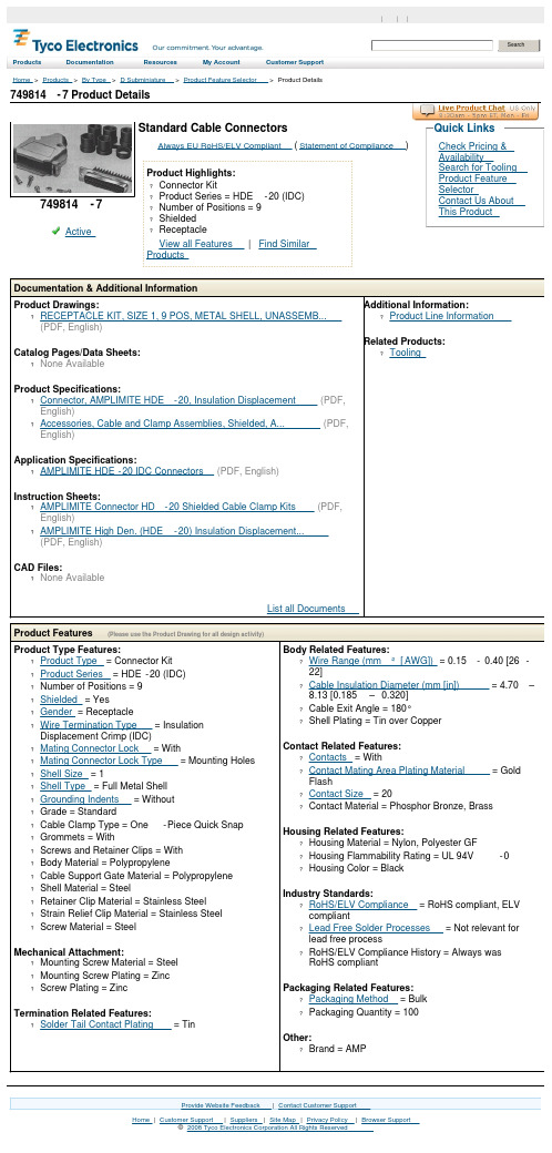
749814-7 Product DetailsHome | Customer Support | Suppliers | Site Map | Privacy Policy | Browser Support© 2008 Tyco Electronics Corporation All Rights Reserved SearchProducts Documentation Resources My Account Customer Support Home > Products > By Type > D Subminiature > Product Feature Selector > Product Details749814-7Active Standard Cable ConnectorsAlways EU RoHS/ELV Compliant (Statement of Compliance)Product Highlights:?Connector Kit?Product Series = HDE-20 (IDC)?Number of Positions = 9?Shielded?ReceptacleView all Features | Find SimilarProductsCheck Pricing &AvailabilitySearch for ToolingProduct FeatureSelectorContact Us AboutThis ProductQuick LinksDocumentation & Additional InformationProduct Drawings:?RECEPTACLE KIT, SIZE 1, 9 POS, METAL SHELL, UNASSEMB...(PDF, English)Catalog Pages/Data Sheets:?None AvailableProduct Specifications:?Connector, AMPLIMITE HDE-20, Insulation Displacement(PDF, English)?Accessories, Cable and Clamp Assemblies, Shielded, A...(PDF, English)Application Specifications:?AMPLIMITE HDE-20 IDC Connectors(PDF, English)Instruction Sheets:?AMPLIMITE Connector HD-20 Shielded Cable Clamp Kits(PDF, English)?AMPLIMITE High Den. (HDE-20) Insulation Displacement...(PDF, English)CAD Files:?None AvailableList all Documents Additional Information:?Product Line InformationRelated Products:?ToolingProduct Features (Please use the Product Drawing for all design activity)Product Type Features:?Product Type = Connector Kit?Product Series = HDE-20 (IDC)?Number of Positions = 9?Shielded = Yes?Gender = Receptacle?Wire Termination Type = InsulationDisplacement Crimp (IDC)?Mating Connector Lock = With?Mating Connector Lock Type = Mounting Holes ?Shell Size = 1?Shell Type = Full Metal Shell?Grounding Indents = Without?Grade = Standard?Cable Clamp Type = One-Piece Quick Snap?Grommets = With?Screws and Retainer Clips = With?Body Material = Polypropylene?Cable Support Gate Material = Polypropylene?Shell Material = Steel?Retainer Clip Material = Stainless Steel?Strain Relief Clip Material = Stainless Steel?Screw Material = SteelMechanical Attachment:?Mounting Screw Material = Steel?Mounting Screw Plating = Zinc?Screw Plating = ZincTermination Related Features:?Solder Tail Contact Plating = Tin Body Related Features:?Wire Range (mm²[AWG]) = 0.15 -0.40 [26-22]?Cable Insulation Diameter (mm [in]) = 4.70 –8.13 [0.185 –0.320]?Cable Exit Angle = 180°?Shell Plating = Tin over CopperContact Related Features:?Contacts = With?Contact Mating Area Plating Material = GoldFlash?Contact Size = 20?Contact Material = Phosphor Bronze, Brass Housing Related Features:?Housing Material = Nylon, Polyester GF?Housing Flammability Rating = UL 94V-0?Housing Color = BlackIndustry Standards:?RoHS/ELV Compliance = RoHS compliant, ELVcompliant?Lead Free Solder Processes = Not relevant forlead free process?RoHS/ELV Compliance History = Always wasRoHS compliantPackaging Related Features:?Packaging Method = Bulk?Packaging Quantity = 100Other:?Brand = AMPProvide Website Feedback | Contact Customer Support。
0874390801;中文规格书,Datasheet资料

Material Info Reference - Drawing Numbers
Product Specification Sales Drawing PS-87437, RPS-87437 SD-87439-001
This document was generated on 08/31/2012
Need more information on product environmental compliance? Email productcompliance@ For a multiple part number RoHS Certificate of Compliance, click here Please visit the Contact Us section for any non-product compliance questions.
Physical
Circuits (maximum) Color - Resin Flammability Gender Glow-Wire Compliant Lock to Mating Part Material - Resin Net Weight Number of Rows Packaging Type Panel Mount Pitch - Mating Interface Polarized to Mating Part Stackable Temperature Range - Operating 8 Natural 94V-0 Female No Yes Nylon 128.000/mg 1 Bag No 1.50mm Yes No -55°C to +105°C
87439-0801 Active
Pico-Spox™ 1.50mm Pitch Pico-SPOX™ Wire-to-Board Housing, 8 Circuits, Black Housing
6424;中文规格书,Datasheet资料
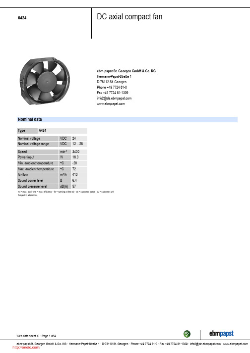
ebm-papst St.Georgen GmbH&Co.KGHermann-Papst-Straße1D-78112St.GeorgenPhone+49772481-0Fax+49772481-1309info2@Nominal dataType6424Nominal voltage VDC24Nominal voltage range VDC12..28Speed min-13400Power input W18.0Min.ambient temperature°C-20Max.ambient temperature°C72Air flow m3/h410Sound power level B 6.4Sound pressure level dB(A)57ml=max.load·me=max.efficiency·fa=running at free air·cs=customer specs·cu=customer unitSubject to alterationsTechnical featuresGeneral description Particular design features:Optional Vario-Pro:Highly flexible software configuration for the fan ensures an easily customisablesolution to meet the individual requirements of your application.General features:Housing made of aluminium,impeller made of fibreglass-reinforced PA;housing with grounding lugfor M4x8screw(Torx).48V version incl.screws.Electronic commutation completely integrated.Protected against reverse polarity and locking.Electrical connection to flat plugs,3x0.5mm.Air exhaust over bars.Direction of rotation counter-clockwise seen on rotor.Mass:760g.Mass0.760kgDimensions172x150x51mmMaterial of impeller Fiberglass-reinforced PA plasticHousing material Aluminum.Housing with grounding lug for screw M4x8(TORX).Direction of air flow Air exhaust over barsDirection of rotation Left,looking at rotorBearing Ball bearingsLifetime L10at40°C75000h35000hLifetime L10at maximumtemperatureConnection line Flat plugs3.0x0.5mm.Motor protection Protected against reverse polarity and locking.Locked-rotor protection Electronic blocking protection,with electronic motor current limit in the startup phase and when therotor is blocked.Approval VDE,CSA,UL,CEProduct drawing LuCharts:Air flow分销商库存信息: EBM-PAPST6424。
TLC084资料
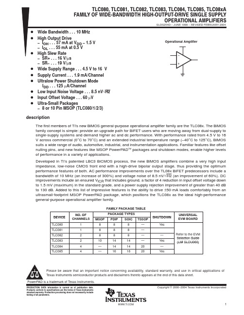
Please be aware that an important notice concerning availability, standard warranty, and use in critical applications of Texas Instruments semiconductor products and disclaimers thereto appears at the end of this data sheet. PowerPAD is a trademark of Texas Instruments.
TLC080 and TLC081 AVAILABLE OPTIONS PACKAGED DEVICES TA 0°C to 70°C SMALL OUTLINE (D)† TLC080CD TLC081CD TLC080ID TLC081ID TLC080AID TLC081AID SMALL OUTLINE (DGN)† TLC080CDGN TLC081CDGN TLC080IDGN TLC081IDGN — — SYMBOL xxTIACW xxTIACY xxTIACX xxTIACZ — — PLASTIC DIP (P) TLC080CP TLC081CP TLC080IP TLC081IP TLC080AIP TLC081AIP
SLOS254D − JUNE 1999 − REVISED FEBRUARY 2004
D Wide Bandwidth . . . 10 MHz D High Output Drive D D D D D D D
− IOH . . . 57 mA at VDD − 1.5 V − IOL . . . 55 mA at 0.5 V High Slew Rate − SR+ . . . 16 V/µs − SR− . . . 19 V/µs Wide Supply Range . . . 4.5 V to 16 V Supply Current . . . 1.9 mA/Channel Ultralow Power Shutdown Mode IDD . . . 125 µA/Channel Low Input Noise Voltage . . . 8.5 nV√Hz Input Offset Voltage . . . 60 µV Ultra-Small Packages − 8 or 10 Pin MSOP (TLC080/1/2/3)
IXGQ85N33PCD1;中文规格书,Datasheet资料
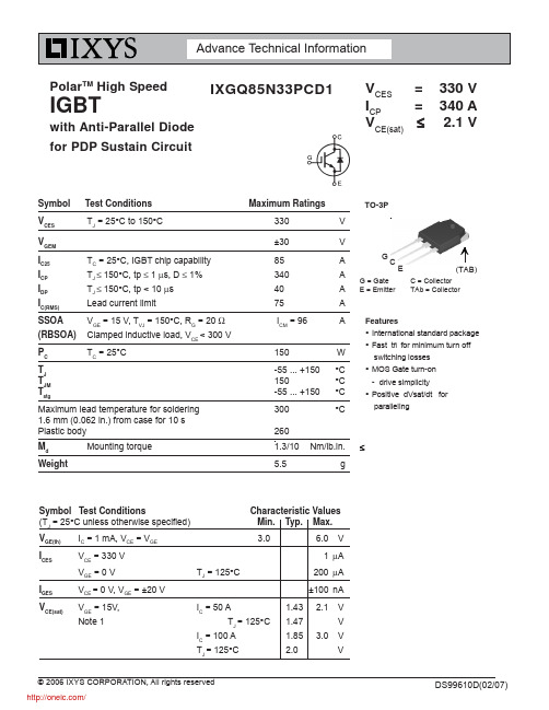
TJ - Degrees Centigrade
Fig. 6. Input Adm ittance
I C - Amperes
140 120 100 80 60 40 20 0 TJ = 125 ºC 25 ºC - 40 ºC 4 4.5 5 5.5 6 6.5 7 7.5 8 8.5 9 9.5
V C E - Volts
4
6
8
10
12
14
16
18
20
22
24
25
50
75
100
125
150
R G - Ohms
T J - Degrees Centigrade
IXYS reserves the right to change limits, test conditions and dimensions.
4.0 3.5 3.0 2.5 2.0 1.5 1.0 5 6 7 8 9
10
11
12
13
14
15
V G E - V olts
V G E - V olts
© 2006 IXYS CORPORATION, All rights reserved /
IXGQ85N33PCD1
TO-3P
TC = 25°C, IGBT chip capability TJ ≤ 150°C, tp ≤ 1 μs, D ≤ 1% TJ ≤ 150°C, tp < 10 μs Lead current limit VGE = 15 V, TVJ = 150°C, RG = 20 Ω Clamped inductive load, VCE < 300 V TC = 25°C
S-80741资料
• • • • • Battery checker Battery backup for memories Power failure detector Reset for microcomputer Store signal detector for nonvolatile RAM
易网
*
S-807 Series will be summarized into S-808 Series.
HIGH-PRECISION VOLTAGE DETECTOR
S-807 Series
The S-807 Series is an adjustment-free high-precision voltage detector made using the CMOS process. The output voltage is fixed internally, with an accuracy of ±2.4%. Two output types are available, Nch opendrain and CMOS output (active “H” and “L”), both of which have various product lineups. This series features much lower current consumption and higher detection voltage accuracy than the S-805 Series. Superminiature package is added for the S-807 Series, the S-807XXSX Series. This small SOT-23-5 style package allows the designer to shrink the size of his finished product. Electrical specs for the S807XXSX Series are the same as the standard S-807 Series. Output forms of the S-807XXSX Series are Nch open-drain and CMOS active “L”.
1809844资料
Extract from the onlinecatalogMSTBC 2,5/13-STZF-5,08Order No.: 1809844The illustration shows a 15-position versionhttp://eshop.phoenixcontact.de/phoenix/treeViewClick.do?UID=1809844Plug component, nominal current: 12 A, rated voltage: 320 V, pitch:5.08 mm, no. of positions: 13, type of connection: Crimp connectionhttp://Please note that the data givenhere has been taken from theonline catalog. For comprehensiveinformation and data, please referto the user documentation. TheGeneral Terms and Conditions ofUse apply to Internet downloads. Technical dataDimensions / positionsPitch 5.08 mmNumber of positions13Technical dataInsulating material group IRated surge voltage (III/3) 4 kVRated surge voltage (III/2) 4 kVRated surge voltage (II/2) 4 kVRated voltage (III/2)320 VRated voltage (II/2)630 VConnection in acc. with standard EN-VDENominal current I N12 ANominal voltage U N320 VNominal cross section 2.5 mm2Maximum load current12 AInsulating material PAInflammability class acc. to UL 94V0Connection dataConductor cross section stranded min.0.5 mm2Conductor cross section stranded max. 2.5 mm2Conductor cross section AWG/kcmil min.20Conductor cross section AWG/kcmil max14Certificates / ApprovalsApproval logoCSANominal voltage U N300 VNominal current I N10 AAWG/kcmil20-14CULNominal voltage U N300 VNominal current I N10 AAWG/kcmil20-14ULNominal voltage U N300 VNominal current I N10 AAWG/kcmil20-14Certification CB, CSA, CUL, UL, VDE-PZIAccessoriesItem Designation DescriptionMarking0804293SK 5,08/3,8:FORTL.ZAHLEN Marker card, printed horizontally, self-adhesive, 12 identicaldecades marked 1-10, 11-20 etc. up to 91-(99)100, sufficient for120 terminal blocksPlug/Adapter1734634CP-MSTB Coding profile, is inserted into the slot on the plug or invertedheader, red insulating material3190564MSTBC-MT 0,5-1,0Module female contact, is inserted into the plug housing MSTBCafter crimping the conductor, for conductors from 0.5 to 1.0 mm²3190645MSTBC-MT 0,5-1,0 BA Module female contact, is inserted into the MSTBC connectorshell after the conductor has been crimped, for conductors from0.5 - 1.0 mm², ribbon contact3190551MSTBC-MT 1,5-2,5Module female contact, is inserted into the plug housing MSTBCafter crimping the conductor, for conductors from 1.5 to 2.5 mm²3190658MSTBC-MT 1,5-2,5 BA Module female contact, is inserted into the MSTBC connectorshell after the conductor has been crimped, for conductors from1.5 -2.5 mm², ribbon contact1810529STZ 2-MSTBC-5,08Strain relief for snapping into the latching chambers of the plugcomponents, 2-pos., labeling with ZB 61810532STZ 4-MSTBC-5,08Strain relief for snapping into the latching chambers of the plugcomponents, 4-pos., labeling with ZB 61810516STZ 8-MSTBC-5,08Strain relief for snapping into the latching chambers of the plugcomponents, 8-pos., labeling with ZB 61810503STZ 12-MSTBC-5,08Strain relief for snapping into the latching chambers of the plugcomponents, 12-pos., labeling with ZB 6Tools1204038CRIMPFOX MT 2,5Crimping pliers, for crimping conductors to the module femalecontacts STG-MTN, crimp range: 0.5-2.5 mm², AWG: 20-14 1205037SZS 0,4X2,5Screwdriver, bladed, matches all screw terminal blocks up to 1.5mm² connection cross section, blade: 0.4 x 2.5 mm Additional productsItem Designation DescriptionGeneral1803060MSTBVK 2,5/13-GF-5,08Header, nominal current: 12 A, rated voltage: 320 V, pitch: 5.08mm, no. of positions: 13, mounting: Mounting rail1788457MVSTBU 2,5/13-GFB-5,08Header, nominal current: 12 A, rated voltage: 320 V, pitch: 5.08mm, no. of positions: 13, mounting: Direct mounting3002034UK 3-MSTB-5,08Modular terminal blocks with plug entry, cross section: 0.2 - 2.5mm², AWG: 30 - 12, width: 5.1 mm, color: gray3002076UK 3-MVSTB-5,08Modular terminal blocks with plug entry, cross section: 0.2 - 2.5mm², AWG: 26 - 12, width: 5.1 mm, color: gray3002102UK 3-MVSTB-5,08-LA 24RD Modular terminal block with plug entry, nominal current: 12 A,rated voltage: 320 V, pitch: 5.08 mm, no. of positions: 1, mounting:mounting rail, with red light indicator, voltage light indicator: 24 VAC/DC, current light indicator: 3.3 mA3002063UK 3-MVSTB-5,08/EK Modular terminal blocks with plug entry, cross section: 0.2-2.5mm², AWG: 26-12, width: 5.1 mm, color: blue3002131UK 3D-MSTBV-5,08Modular terminal blocks with vertical plug entry, cross section: 0.2- 2.5 mm, AWG: 30 - 12, width: 5.1 mm, color: gray3002144UK 3D-MSTBV-5,08-LA 24RD Modular terminal block with vertical plug entry, color: Gray, withred light indicator, voltage light indicator: 24 V AC/DC, current lightindicator: 3.3 mA3002173UK 3D-MSTBV-5,08/EK Modular terminal blocks with plug entry, cross section: 0.2 - 2.5mm², AWG: 30 - 12, width: 5.1 mm, color: blue2770888UKK 3-MSTB-5,08Modular terminal blocks with 2 horizontal plug entries, crosssection: 0.2 - 2.5 mm, AWG: 30 - 12, width: 5.1 mm, color: gray 1876615UKK 3-MSTB-5,08-PE Ground terminal block, with 2 horizontal plug entries, nominalcurrent: 12 A, rated voltage: 320 V, pitch: 5.08 mm, no. ofpositions: 1, mounting: mounting rail.1788033UMSTBVK 2,5/13-GF-5,08Header, nominal current: 12 A, rated voltage: 320 V, pitch: 5.08mm, no. of positions: 13, mounting: Mounting rail1873016ZFKK 1,5-MSTBV-5,08Modular terminal blocks with plug entry, cross section: 0.2 - 1.5mm², width: 5.1 mm, color: grayDrawingsDimensioned drawingAddressPHOENIX CONTACT GmbH & Co. KGFlachsmarktstr. 832825 Blomberg,GermanyPhone +49 5235 3 00Fax +49 5235 3 41200http://www.phoenixcontact.de© 2008 Phoenix ContactTechnical modifications reserved;。
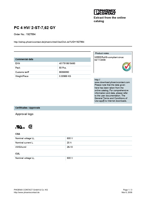
1927894资料
PHOENIX CONTACT GmbH & Co. KG http://www.phoenixcontact.de
Page 3 / 3 Mar 6, 2008
Product notes Commercial data EAN Pack Customs tariff Weight/Piece 4017918618490 50 Pcs. 85366990 0.00955 KG http:// Please note that the data given here has been taken from the online catalog. For comprehensive information and data, please refer to the user documentation. The General Terms and Conditions of Use apply to Internet downloads. Certificates / Approvals WEEE/RoHS-compliant since: 02/11/2005
元器件交易网
Extract from the online catalog
PC 4 HV/ 2-ST-7,62 GY
Order No.: 1927894
http://eshop.phoenixcontact.de/phoenix/treeViewClick.do?UID=1927894
Nominal current IN AWG/kcmil UL Nominal voltage UN Nominal current IN AWG/kcmil Certifica30-10 CSA, CUL, UL
PHOENIX CONTACT GmbH & Co. KG http://www.phoenixcontact.de
