利用精密模拟微控制器构建 4 mA 至 20 mA 环路供电温度监控器
4到20mA模拟恒流环路信号发生器制作

4到20mA模拟恒流环路信号发生器制作一。
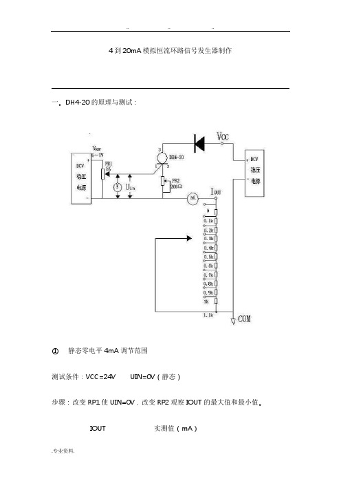
DH4-20的原理与测试:①静态零电平4mA调节范围测试条件:VCC=24V UIN=0V(静态)步骤:改变RP1使UIN=0V,改变RP2观察IOUT的最大值和最小值。
IOUT实测值(mA)RP2↓最小值3mA±0.3mA 2.790RP2↑最大值5mA±0.3mA 4.838②UIN-IOUT线性测试测试条件:VCC=24V RL=700Ω步骤:1.将RP1调至UIN=0V2将RP2调至IOUT=4.000mA3.改变RP1从0~5V的UIN电位UIN(V)IOUT(mA)实测值(mA)0 4.000 4.0021.2508.0007.9972.50012.000 11.9983.75016.000 16.0035.000 20.000 20.008③RL-VCC最大负载电阻与工作电压之间的关系测试条件:在上述②的测试条件UIN=5V,IOUT=20mA恒定状态下步骤:改变以下RL与VCC的对应关系,观察IOUT=20mA恒定状态RL(KΩ)VCC(V)实测值(mA)0 1020.0030.11220.0030.21420.0050.31620.0050.41820.0050.52020.0050.62220.0050.72420.0050.82620.0100.92820.0101.03020.0101.13220.010④满值20mA的恒流测试测试条件:VCC=24V IOUT=20.000mA步骤:在上述条件下,改变RL从0~0.7KΩ,观察满值20的恒定状态RL(KΩ)IOUT实测值(mA)0 20.0210.120.0200.220.0190.320.0170.420.0160.520.0150.620.0140.720.013二。
二线制4~20mA模拟恒流环路信号发生器制作三。
二线制4~20mA模拟恒流环路信号发生器制作指标要求以精度0.5级为例,二线制4~20mA模拟恒环路信号发生器执行标准:GB/T13850-1998;(1)基准要稳,4mA是对应的输入零位基准,基准不稳,谈何精度线性度,冷开机3分锺内4mA 的零位漂移变化不超过4.000mA0.5%以内;(即3.98-4.02mA),负载250Ω上的压降为0.995-1.005V,国外IC心片多用昂贵的能隙基准,温漂系数每度变化10ppm;(2)内电路总计消耗电流<4mA,加整定后等于4.000mA,而且有源整流滤波放大恒流电路不因原边输入变化而消耗电流也随之变化,国外IC心片采用恒流供电;(3)当工作电压24.000V时,满量程20.000mA时,满量程20.000mA的读数不会因负载0-700Ω变化而变化;变化不超过20.000mA0.5%以内;(4)当满量程20.000mA时,负载250Ω时,满量程20.000mA的读数不会因工作电压15.000V-30.000V变化而变化;变化不超过20.000mA0.5%以内;(5)当原边过载时,输出电流不超过25.000mA+10%以内,否则PLC/DCS内供变送器用的24V工作电源和A/D输入箝位电路因功耗过大而损坏,另外变送器内的射随输出亦因功耗过大而损坏,无A/D输入箝位电路的更遭殃;(6)当工作电压24V接反时不得损坏变送器,必须有极性保护;(7)当两线之间因感应雷及感应浪涌电压超过24V时要箝位,不得损坏变送器;一般在两线之间并联1-2只TVS瞬态保护二极管 1.5KE可抑制每20秒间隔一次的20毫秒脉宽的正反脉冲的冲击,瞬态承受冲击功率1.5KW-3KW;(8)产品标示的线性度0.5%是绝对误差还是相对误差,可以按以下方法来辨别方可一目了然:符合下述指标是真的线性度0.5%.原边输入为零时输出4mA正负0.5%(3.98-4.02mA),负载250Ω上的压降为0.995-1.005V原边输入10%时输出5.6mA正负0.5%(5.572-5.628mA)负载250欧姆上的压降为1.393-1.407V原边输入25%时输出8mA正负0.5%(7.96-8.04mA)负载250Ω上的压降为1.990-2.010V原边输入50%时输出12mA正负0.5%(11.94-12.06mA)负载250Ω上的压降为2.985-3.015V原边输入75%时输出16mA正负0.5%(15.92-16.08mA)负载250Ω上的压降为3.980-4.020V原边输100%时输出20mA正负0.5%(19.90-20.10mA)负载250Ω上的压降为4.975-5.025V(9)原边输入过载时必须限流:原边输入过载大于125%时输出过流限制25mA+10%(25.00-27.50mA)负载250Ω上的压降为6.250-6.875V;(10)感应浪涌电压超过24V时有无箝位的辨别:在两线输出端口并一个交流50V指针式表头,用交流30-35V接两根线去瞬间碰一下两线输出端口,看有无箝位,箝位多少伏可一目了然啦;(11)有无极性保护的辨别:用指针式万用表Ω乘10K档正反测量两线输出端口,总有一次Ω阻值无限大,就有极性保护;(12)有无极输出电流长时间短路保护:原边输入100%时或过载大于125%-200%时,将负载250Ω短路,测量短路保护限制是否在25mA+10%;(13)工业级别和民用商用级别的辨别:工业级别工作温度范围是-25度到+70度,温漂系数是每度变化100ppm,即温度每度变化1度,精度变化为万分之一;民用商用级别工作温度范围是0度(或-10度)到+70度(或+50度),温漂系数是每度变化250ppm,即温度每度变化1度,精度变化为万分之二点五;DH4~20mA模拟串口模块及其变送器电路设计中国科学院半导体所方舟公司李德辉摘要:二线制4~20mA模拟串口环路作为电流遥测技术标准,以其众多优点得到广泛应用,本文介绍的DH4~20型DH4~20mA模拟串口模块与无源交流隔离传感器的组合,不但解决了交流电流电压信号的二线制4~20mA环路遥测问题,而且成本低,性价比高。
LTC4054-4.2中文资料
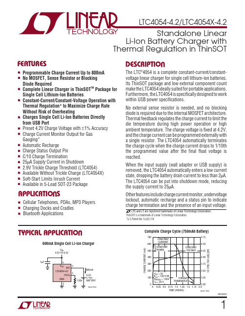
LTC4054-4.2/LTC4054X-4.2 Standalone Linear Li-Ion Battery Charger with Thermal Regulation in ThinSOT
FEATURES
s s
DESCRIPTIO
s
s
s
s s
s s s s s s s s
Cellular Telephones, PDAs, MP3 Players Charging Docks and Cradles Bluetooth Applications
TYPICAL APPLICATIO
VIN 4.5V TO 6.5V
Complete Charge Cycle (750mAh Battery)
The LTC®4054 is a complete constant-current/constantvoltage linear charger for single cell lithium-ion batteries. Its ThinSOT package and low external component count make the LTC4054 ideally suited for portable applications. Furthermore, the LTC4054 is specifically designed to work within USB power specifications. No external sense resistor is needed, and no blocking diode is required due to the internal MOSFET architecture. Thermal feedback regulates the charge current to limit the die temperature during high power operation or high ambient temperature. The charge voltage is fixed at 4.2V, and the charge current can be programmed externally with a single resistor. The LTC4054 automatically terminates the charge cycle when the charge current drops to 1/10th the programmed value after the final float voltage is reached. When the input supply (wall adapter or USB supply) is removed, the LTC4054 automatically enters a low current state, dropping the battery drain current to less than 2µA. The LTC4054 can be put into shutdown mode, reducing the supply current to 25µA. Other features include charge current monitor, undervoltage lockout, automatic recharge and a status pin to indicate charge termination and the presence of an input voltage.
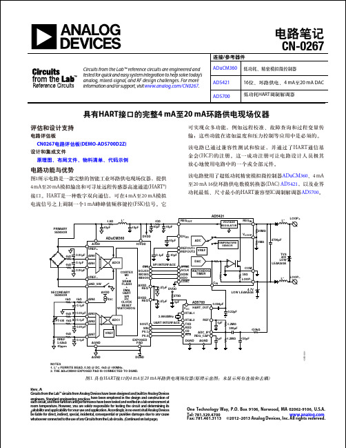
ADI电路参考设计CN-0382说明书

电路笔记CN-0382Circuits from the Lab® reference designs are engineered and tested for quick and easy system integration to help solve today’s analog, mixed-signal, and RF design challenges. For more information and/or support, visit /CN0382.连接/参考器件AD7124-4 集成PGA和基准电压源的低功耗24位Σ-Δ型ADCAD5421 16位、环路供电、4 mA至20 mA DAC AD5700 低功耗HART调制解调器SPI隔离器ADuM1441ADP162超低静态电流、150 mA CMOS线性稳压器ADG5433高压防闩锁型三通道SPDT开关Rev. 0Circuits from the Lab® reference designs from Analog Devices have been designed and built by Analog Devices engineers. Standard engineering practices have been employed in the design and construction of each circuit, and their function and performance have been tested and veri ed in a labenvironment at room temperature. However, you are solely responsible for testing the circuit and determining its suitability and applicability for your use and application. Accordingly, in no event shall Analog Devices be liable for direct, indirect, special, incidental, consequential or punitive damages due to any cause whatsoever connected to the use of any Circ uits from the Lab circuits. (Continued on last page) One Technology Way, P.O. Box 9106, Norwood, MA 02062-9106, U.S.A. Tel: 781.329.4700 Fax: 781.461.3113 ©2015 Analog Devices, Inc. All rights reserved.采用低功耗、精密、24位Σ-Δ型ADC的隔离式4 mA至20 mA/HART工业温度和压力变送器评估和设计支持电路评估板DEM O-AD7124-DZ评估板设计和集成文件原理图、布局文件、物料清单、代码示例电路功能与优势图1所示电路是一种隔离式智能工业现场仪表,可与许多类型的模拟传感器,如温度传感器(Pt100、Pt1000、热电偶)或桥式压力传感器等接口。
FT742 (4-20mA)风传感器用户手册说明书

FT TECHNOLOGIES LTD 18 CHURCH ROAD TEDDINGTONMIDDLESEX, TW11 8PD电话: +44 (0)20 8943 0801 传真: +44 (0)20 8943 3283 网址: E-MAIL: ***************.ukA4277-1-CN2017年1月. FT 和 Acu-Res (声共振)标识为FT Technologies 公司注册商标 The FT and Acu-Res logos are registered trademarks of FT Technologies Ltd. Copyright © 2017 FT Technologies Ltd. All rights reserved.FT742 - 模拟型 (4-20mA)风传感器手册管状直接安装方式目录产品标识 (3)Safety Instructions (4)安全须知 (5)1简介 (6)1.1产品概述 (6)1.2产品版本型号与标识 (6)1.3使用范围 (6)1.4声明 (7)2功能描述 (8)2.1技术性能 (8)2.2电流回路 (9)2.2.1电流回路特征 (9)2.2.2均值滤波器特征 (9)2.2.3风速回路 (9)2.2.4风向回路 (10)2.2.5调整风向基准 (11)2.2.6错误检测 (12)2.3加热器设置 (13)2.4低能耗运行 (13)3机械和电气安装 (14)3.1连接器细节 (21)3.2电缆细节 (21)3.3雷击、浪涌与电磁干扰(EMI)防护 (21)4服务、设置与测试 (23)4.1检测 (23)4.2故障查找与故障排除 (24)4.3退货条款 (25)4.4Acu Test 测评套装 (26)4.4.1Acu Test电脑测试评估软件 (26)4.4.2FT055 测试电缆 (27)产品标识本使用手册及相关设备将使用以下标识。
DEMO-AD5700D2Z电路笔记中文版
CN-0267
电路描述 模拟前端接口
ADuCM360模拟前端集成双通道、高性能、24位Σ-Δ型模 数转换器(ADC)。同时还集成了可编程增益仪表放大器、 精密带隙基准电压源、可编程电流源、灵活的多路复用器 以及其它许多特性。该器件允许直接与多个模拟传感器对 接,如压力传感器电桥、电阻式温度传感器、热电偶以及 工业用途的其它各类传感器。
例如,若控制器和AD5421之间的通信发生故障,AD5421 将在一段时间后自动设置其模拟输出为3.2 mA报警电流。 此报警电流将现场仪器工作故障这一情况汇报给主机。
输出电流值的任何改变都受到软件的控制,以防对HART 通信产生干扰。(参见“模拟变化率”部分)。
HART通信 AD5700集成完整的HART FSK调制解调器。该调制解调器 通过标准UART接口,伴随请求发送(RTS)和载波检测(CD) 信号实现与ADuCM360控制器的连接。
电源和电源管理 包括传感器驱动电流在内的完整现场仪器电路必须工作在 4 mA至20 mA环路提供的限量电源下。这对所有环路供电 现场仪器设计而言,都是一个普遍的难题。图1中的电路 提供了低功耗以及高性能解决方案的一个实例。应用中用 到的全部三个集成电路均针对低功耗而设计,并且电路依 靠各自的集成特性提供灵活的电源管理结构和性能最优的 环路供电解决方案。
CD
ADC_IP
RTS REG_CAP
DGND AGND
CIN 0.068µF
1µF 1µF
COM 50Ω LOOP–
4.7V LOW LEAKAGE
0.22µF
1.2MΩ 300pF
150kΩ
1.2MΩ 150pF
L* LOOP+
4700pF
TVS 40V LOW LEAKAGE
ROHM Solution Simulator 用户指南.pdf_1705892277.949866
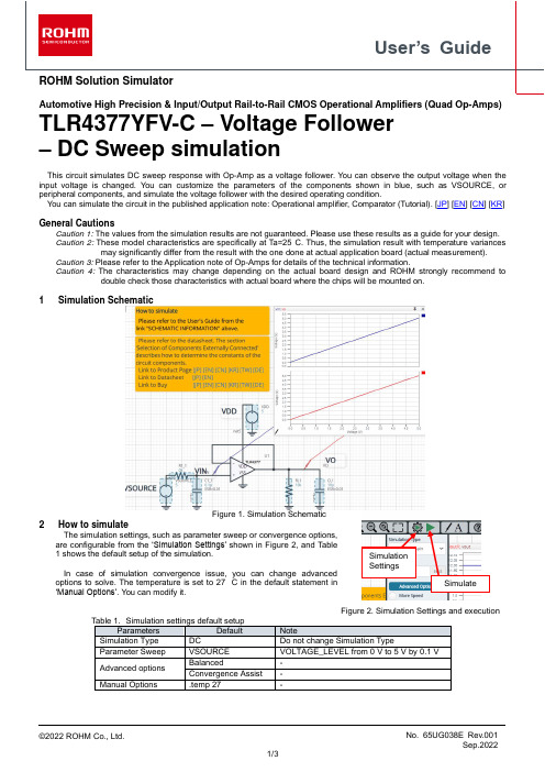
User’s Guide ROHM Solution SimulatorAutomotive High Precision & Input/Output Rail-to-Rail CMOS Operational Amplifiers (Quad Op-Amps) TLR4377YFV-C – Voltage Follower– DC Sweep simulationThis circuit simulates DC sweep response with Op-Amp as a voltage follower. You can observe the output voltage when the input voltage is changed. You can customize the parameters of the components shown in blue, such as VSOURCE, or peripheral components, and simulate the voltage follower with the desired operating condition.You can simulate the circuit in the published application note: Operational amplifier, Comparator (Tutorial). [JP] [EN] [CN] [KR] General CautionsCaution 1: The values from the simulation results are not guaranteed. Please use these results as a guide for your design.Caution 2: These model characteristics are specifically at Ta=25°C. Thus, the simulation result with temperature variances may significantly differ from the result with the one done at actual application board (actual measurement).Caution 3: Please refer to the Application note of Op-Amps for details of the technical information.Caution 4: The characteristics may change depending on the actual board design and ROHM strongly recommend to double check those characteristics with actual board where the chips will be mounted on.1 Simulation SchematicFigure 1. Simulation Schematic2 How to simulateThe simulation settings, such as parameter sweep or convergence options,are configurable from the ‘Simulation Settings’ shown in Figure 2, and Table1 shows the default setup of the simulation.In case of simulation convergence issue, you can change advancedoptions to solve. The temperature is set to 27 °C in the default statement in‘Manual Options’. You can modify it.Figure 2. Simulation Settings and execution Table 1.Simulation settings default setupParameters Default NoteSimulation Type DC Do not change Simulation TypeParameter Sweep VSOURCE VOLTAGE_LEVEL from 0 V to 5 V by 0.1 VAdvanced options Balanced - Convergence Assist -Manual Options .temp 27 - SimulationSettingsSimulate3 Simulation Conditions4 Op-Amp modelTable 3 shows the model pin function implemented. Note that the Op-Amp model is the behavior model for its input/output characteristics, and no protection circuits or the functions not related to the purpose are not implemented.5 Peripheral Components5.1 Bill of MaterialTable 4 shows the list of components used in the simulation schematic. Each of the capacitors has the parameters of equivalent circuit shown below. The default values of equivalent components are set to zero except for the ESR ofC. You can modify the values of each component.Table 4. List of capacitors used in the simulation circuitType Instance Name Default Value Variable RangeUnits Min MaxResistor R1_1 0 0 10 kΩRL1 10k 1k 1M, NC ΩCapacitor C1_1 0.1 0.1 22 pF CL1 10 free, NC pF5.2 Capacitor Equivalent Circuits(a) Property editor (b) Equivalent circuitFigure 3. Capacitor property editor and equivalent circuitThe default value of ESR is 0.01 Ω.(Note 2) These parameters can take any positive value or zero in simulation but it does not guarantee the operation of the IC in any condition. Refer to the datasheet to determine adequate value of parameters.6 Recommended Products6.1 Op-AmpTLR4377YFV-C : Automotive High Precision & Input/Output Rail-to-Rail CMOS Operational Amplifier (QuadOp-Amp). [JP] [EN] [CN] [KR] [TW] [DE]TLR2377YFVM-C : Automotive High Precision & Input/Output Rail-to-Rail CMOS Operational Amplifier (DualOp-Amp). [JP] [EN] [CN] [KR] [TW] [DE]TLR377YG-C : Automotive High Precision & Input/Output Rail-to-Rail CMOS Operational Amplifier. [JP] [EN] [CN] [KR] [TW] [DE]LMR1802G-LB : Low Noise, Low Input Offset Voltage CMOS Operational Amplifier. [JP] [EN] [CN] [KR] [TW] [DE] Technical Articles and Tools can be found in the Design Resources on the product web page.NoticeROHM Customer Support System/contact/Thank you for your accessing to ROHM product informations.More detail product informations and catalogs are available, please contact us.N o t e sThe information contained herein is subject to change without notice.Before you use our Products, please contact our sales representative and verify the latest specifica-tions :Although ROHM is continuously working to improve product reliability and quality, semicon-ductors can break down and malfunction due to various factors.Therefore, in order to prevent personal injury or fire arising from failure, please take safety measures such as complying with the derating characteristics, implementing redundant and fire prevention designs, and utilizing backups and fail-safe procedures. ROHM shall have no responsibility for any damages arising out of the use of our Poducts beyond the rating specified by ROHM.Examples of application circuits, circuit constants and any other information contained herein areprovided only to illustrate the standard usage and operations of the Products. The peripheral conditions must be taken into account when designing circuits for mass production.The technical information specified herein is intended only to show the typical functions of andexamples of application circuits for the Products. ROHM does not grant you, explicitly or implicitly, any license to use or exercise intellectual property or other rights held by ROHM or any other parties. ROHM shall have no responsibility whatsoever for any dispute arising out of the use of such technical information.The Products specified in this document are not designed to be radiation tolerant.For use of our Products in applications requiring a high degree of reliability (as exemplifiedbelow), please contact and consult with a ROHM representative : transportation equipment (i.e. cars, ships, trains), primary communication equipment, traffic lights, fire/crime prevention, safety equipment, medical systems, servers, solar cells, and power transmission systems.Do not use our Products in applications requiring extremely high reliability, such as aerospaceequipment, nuclear power control systems, and submarine repeaters.ROHM shall have no responsibility for any damages or injury arising from non-compliance withthe recommended usage conditions and specifications contained herein.ROHM has used reasonable care to ensur e the accuracy of the information contained in thisdocument. However, ROHM does not warrants that such information is error-free, and ROHM shall have no responsibility for any damages arising from any inaccuracy or misprint of such information.Please use the Products in accordance with any applicable environmental laws and regulations,such as the RoHS Directive. For more details, including RoHS compatibility, please contact a ROHM sales office. ROHM shall have no responsibility for any damages or losses resulting non-compliance with any applicable laws or regulations.W hen providing our Products and technologies contained in this document to other countries,you must abide by the procedures and provisions stipulated in all applicable export laws and regulations, including without limitation the US Export Administration Regulations and the Foreign Exchange and Foreign Trade Act.This document, in part or in whole, may not be reprinted or reproduced without prior consent ofROHM.1) 2)3)4)5)6)7)8)9)10)11)12)13)。
4-20mA Display Installation and Operation Manual
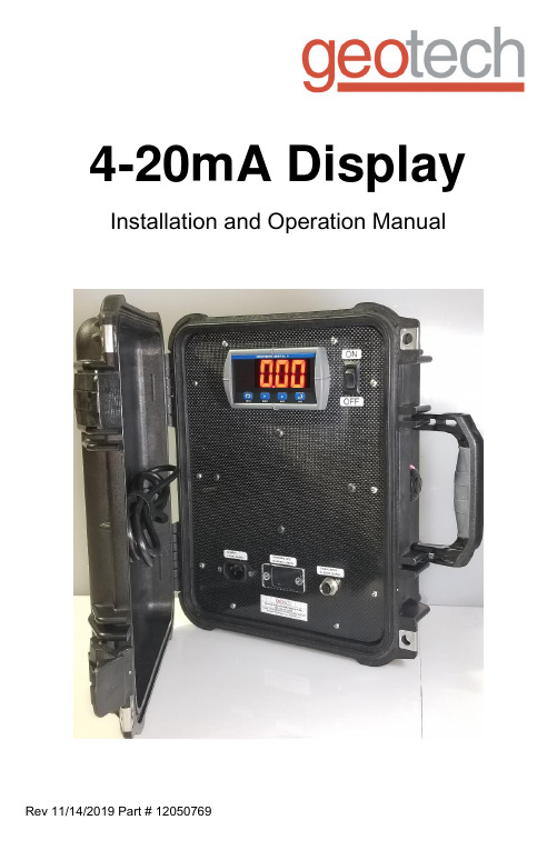
4-20mA Display Installation and Operation ManualTable of ContentsDOCUMENTATION CONVENTIONS (2)Section 1: System Description (3)Function and Theory (3)Section 2: System Installation (4)Wiring the transducer (4)Setting Display Units (5)Section 3: System Operation (9)Quick Start Guide (9)Section 4: System Maintenance (9)Section 5: System Troubleshooting (10)Section 6: System Specifications (11)Section 7: Parts and Accessories (11)The Warranty (13)DOCUMENTATION CONVENTIONS This uses the following conventions to present information:An exclamation point icon indicates a WARNING of a situationor condition that could lead to personal injury or death. Youshould not proceed until you read and thoroughly understand theWARNING message.WARNINGCAUTIONA raised hand icon indicates CAUTION information that relates toa situation or condition that could lead to equipment malfunctionor damage. You should not proceed until you read and thoroughlyunderstand the CAUTION message.A note icon indicates NOTE information. Notes provide additionalor supplementary information about an activity or concept.NOTESection 1: System DescriptionFunction and TheoryThe Geotech 4-20mA Display is a display for 4-20mA sensors. Specifically designed for harsh environments, the LED screen displays clear pressure or water level read outs while the sensor is attached. The display can be easily reprogrammed through the interface to accommodate a variety of sensors.System ComponentsPower Switch DisplayAC Input (Charging plug) Battery Status Signal Input(Sensor Connection)EnclosureSection 2: System InstallationWiring the transducer1. Open the connector.2. Remove all internal components of the connector.3. Slide the components separately over the cable.4. Ensure 1/8” of the cable is past the rubber part of the strain relief.5. Wire cable to the connector using the following diagram+ VDCmA Signal Return Ground/Shielding WireFigure 1-16. Completely re-assemble the connector.7. Plug the 4-20mA transducer into the “4-20mA signal input” on the control panel The transducer is now be ready to use with the 4-20mA Display.The 4-20mA display comes pre-set from Geotech to operate with a 0-30 PSI transducer and display PSI. If a different range is used (i.e. 0-50PSI) or you would like the display to show water level, use the following steps to change the display.Setting Display Units1. Switch the ON/OFF switch to the ON position.∙If the transducer is plugged into the unit then the screen will display a 0 value.o EX 0.00; 0.01 etc.∙If the transducer is not plugged into the unit, then the screen will displaya negative value that corresponds with the PSI/FT setting of the unit.o EX: If the unit is scaled to display PSI for a 0-5PSI transducerthen the display will read a negative value of approximately -3.7when the transducer is not plugged in.2. Press the MENU key to enter Programming mode.3. Press ACK key to access the Setup menu.4. Press the ACK key to access the Input menu5. Select 4-20mA and press the ACK key to confirm the selection input.∙This is the default option. If 4-20mA is not the default, press the MAX key to scroll through the choices.6. Press the ACK key to access the Decimal Point menu.7. Select the decimal place by pressing the MAX key.∙PSI decimal placement: ddd.d∙FEET decimal placement: ddd.d8. Press the ACK key to confirm input selection9. Press the ACK key to enter the Program menu.10. Press the ACK key to enter the Scale menu.11. Press the ACK to access the Input 1 menu.∙This input represents 0% of the process variable.∙The default value of 4.00mA should be sufficient for most applications.12. Press the ACK key to accept.13. Press the ACK key to access Display 1.∙This is the value that will be displayed on the meter when the input is 4mA∙The display will read “0” at this input.14. Press the ACK key to enter Input 2.∙The default input value of 20.00 for input 2 should be sufficient.15. Press the ACK to accept this value.16. Press the ACK key to enter Display 2.17. At this point it will be determined if the meter will display PSI or Feet.If the meter is to display in PSI then set the display number to the max PSIrating on the sensor using step #18.Ex. For a 0-30psi sensor, set the display to 30.If the meter is to display in Feet then determine the max depth by using thefollowing calculation:FtMax= 2.31 x (Pressure rating)EX: If a 0-15PSI sensor is being used, then the equation will be:FtMax = 2.31 x 15FtMax = 34.65ftSet the display number to the calculated FtMax using step #18.18. Enter the desired number in the Display 2 screen by pressing the RESET keyto select the digit (the selected digit is brighter than the others are). Press theMAX key to increment the digits. Once the number is set, press the ACK keyto accept the input.19. Press the MENU key to return to run mode.Section 3: System OperationSystem will display reading while powered ON.The battery depletes after approximately 8 hours.Recharge the system by turning the ON/OFF switch to the OFF position, unplug the transducer, and plug in the power cable (provided with the unit) until the charging light turns green.Quick Start Guide1) Plug in the wired transducer. Ensure wiring matches Figure 1-12) Turn the unit on with the ON/OFF switch.3) Ensure to set the desired display units using steps 1-19 from the installationsection.4) The unit is now ready for use.Section 4: System MaintenanceClean faceplate and case with mild soaps as needed.Do not store in direct sunlight.Charge battery before long-term storageSection 5: System TroubleshootingProblem: Display not receiving a signal from the transducer.Solution: Verify wiring according to Figure 1-1Problem: No displaySolution: Power unit OFF and ON. If the screen remains blank, contact Geotech. Solution: Charge unit.Problem: Water in the enclosure.Solution: Open the faceplate by removing all 10 silver screws with a Philips screwdriver. Remove water from the enclosure. Wipe case and components with a dry cloth. Ensure case and components are completely dry before reassembling.Problem: Screen suddenly turns offSolution: The components may be too hot. Let it cool down before resuming.Check the power.Problem: Display is reading a negative number while the transducer is plugged into the unit.Solution: Check wiring. Ensure wiring matches Figure 1-1.Section 6: System SpecificationsLED Panel MeterDisplay Digit Height .56”, 4 digits, red LED(14.2mm)Display Category LED, Single Line Transmitter Power NoneOperating Temperature Range 32°F - 149°F (0°C - 65°C)Power 85-265 VAC, 90-265 VDCOutput Options 4-20 mAInput Current (4-20 mA), Voltage (0-10 V) Thermocouple,RTDAccuracy +/- 1%Display Intensity 8 user-selectable intensity levelsSpecial Features Sunlight readable displayEnclosureEnclosure 6 x 13.4 x 11.6 in. (18 x 48 x 35 cm)Enclosure Material Structural resinBattery Performance @ 70°F12V 9AH Battery Life 50,000 cyclesInternal Battery Life (2x 9V, alkaline)30,000 cyclesSection 7: Parts and AccessoriesDescription Part Number CORD, POWER, 6’ 7” (B)12070014 CONNECTOR, SERVICE, PT2X 7A23102, 8A6V121, SEA 12106022The WarrantyFor a period of one (1) year from date of first sale, product is warranted to be free from defects in materials and workmanship. Geotech agrees to repair or replace, at Geotech’s option, the portion proving defective, or at our option to refund the purchase price thereof. Geotech will have no warranty obligation if the product is subjected to abnormal operating conditions, accident, abuse, misuse, unauthorized modification, alteration, repair, or replacement of wear parts. User assumes all other risk, if any, including the risk of injury, loss, or damage, direct or consequential, arising out of the use, misuse, or inability to use this product. User agrees to use, maintain and install product in accordance with recommendations and instructions. User is responsible for transportation charges connected to the repair or replacement of product under this warranty.Equipment Return PolicyA Return Material Authorization number (RMA #) is required prior to return of any equipment to our facilities, please call our 800 number for appropriate location. An RMA # will be issued upon receipt of your request to return equipment, which should include reasons for the return. Your return shipment to us must have this RMA # clearly marked on the outside of the package. Proof of date of purchase is required for processing of all warranty requests.This policy applies to both equipment sales and repair orders.FOR A RETURN MATERIAL AUTHORIZATION, PLEASE CALL OURSERVICE DEPARTMENT AT 1-800-833-7958.Model Number: ________________Serial Number: ________________Date of Purchase: ________________Equipment DecontaminationPrior to return, all equipment must be thoroughly cleaned and decontaminated. Please make note on RMA form, the use of equipment, contaminants equipment was exposed to, and decontamination solutions/methods used. Geotech reserves the right to refuse any equipment not properly decontaminated. Geotech may also choose to decontaminate the equipment for a fee, which will be applied to the repair order invoice.Geotech Environmental Equipment, Inc.2650 East 40th Avenue Denver, Colorado 80205 (303) 320-4764 ● (800) 833-7958 ● FAX (303) 322-7242。
4到20mA模拟恒流环路信号发生器制作
4到20mA模拟恒流环路信号发生器制作一。
DH4-20的原理与测试:①静态零电平4mA调节范围测试条件:VCC=24V UIN=0V(静态)步骤:改变RP1使UIN=0V,改变RP2观察IOUT的最大值和最小值。
IOUT 实测值(mA)RP2↓最小值3mA±0.3mA 2.790RP2↑最大值5mA±0.3mA 4.838② UIN-IOUT线性测试测试条件:VCC=24V RL=700Ω步骤:1.将RP1调至UIN=0V2将RP2调至IOUT=4.000mA3.改变RP1从0~5V的UIN电位UIN (V) IOUT(mA)实测值(mA)0 4.000 4.0021.250 8.000 7.9972.500 12.000 11.9983.750 16.000 16.0035.000 20.000 20.008③RL-VCC最大负载电阻与工作电压之间的关系测试条件:在上述②的测试条件UIN=5V,IOUT=20mA恒定状态下步骤:改变以下RL与VCC的对应关系,观察IOUT=20mA恒定状态 RL(KΩ) VCC(V)实测值(mA)0 10 20.0030.1 12 20.0030.2 14 20.0050.3 16 20.0050.4 18 20.0050.5 20 20.0050.6 22 20.0050.7 24 20.0050.8 26 20.0100.9 28 20.0101.0 30 20.0101.1 32 20.010④满值20mA的恒流测试测试条件:VCC=24V IOUT=20.000mA步骤:在上述条件下,改变RL从0~0.7KΩ,观察满值20的恒定状态 RL(KΩ) IOUT实测值(mA)0 20.0210.1 20.0200.2 20.0190.3 20.0170.4 20.0160.5 20.0150.6 20.0140.7 20.013二。
二线制4~20mA模拟恒流环路信号发生器制作三。
4到20mA模拟输出应用笔记
4~20mA模拟输出(电流环)应用笔记bpesun@前言4-20mA.DC(1-5V.DC)信号制是国际电工委员会(IEC):过程控制系统用模拟信号标准。
在工业现场,如果采集的信号经调理后是电压信号并且进行长线传输,会产生以下问题:第一,由于传输的信号是电压信号,传输线会很容易就受到噪声的干扰;第二,传输线的分布电阻会产生电压降;第三,在现场如何提供仪表放大器的工作电压也是个问题。
为了解决上述问题和避开相关噪声的影响,工业现场大量采用电流来传输信号。
采用电流信号的原因是不容易受干扰。
并且电流源内阻无穷大,导线电阻串联在回路中不影响精度,在普通双绞线上可以传输数百米。
上限取20mA是因为防爆的要求:20mA的电流通断引起的火花能量不足以引燃瓦斯,而低于4mA高于20mA的信号用于各种故障的报警下限。
只所以没有取0mA的原因是为了能检测断线:正常工作时不会低于4mA,当传输线因故障断路,环路电流降为0。
4~20mA电流环有两种类型:二线制和三线制。
当监控系统需要通过长线驱动现场的驱动器件如阀门等时,一般采用三线制变送器,这里电流输出模块位于监控的系统端,由系统直接向电流输出模块供电,供电电源是二根电流传输线以外的第三根线。
二线系统是电流输出模块和传感器位于现场端,由于现场供电困难,一般是接收端利用4~20mA的电流环线缆向远端的电流输出模块供电,通过4~20mA来反映信号的大小。
4~20mA产品的典型应用是传感和测量应用。
在工业现场有许多种类的传感器可以被转换成4~20mA的电流信号。
变送器的概念是将非标准电信号转换为标准电信号(0/4~20mA DC,1~5V DC,0~10V DC)的仪器。
传感器是能够受规定的被测量并按照一定的规律转换成可用输出信号的器件或装置的总称,通常由敏感元件和转换元件组成。
当传感器的输出为规定的标准信号时,则称为变送器。
们讨论的两线制、三线制、四线制,是指各种输出为模拟直流电流信号的变送器。
4~20mA电流环与信号隔离器原理及应用

4~20mA电流环工作原理2008-04-07 22:40在工业现场,用一个仪表放大器来完成信号的调理并进行长线传输,会产生以下问题:第一,由于传输的信号是电压信号,传输线会受到噪声的干扰;第二,传输线的分布电阻会产生电压降;第三,在现场如何提供仪表放大器的工作电压也是个问题。
为了解决上述问题和避开相关噪声的影响,我们用电流来传输信号,因为电流对噪声并不敏感。
4~20mA的电流环便是用4mA表示零信号,用20mA表示信号的满刻度,而低于4mA高于20mA的信号用于各种故障的报警。
4~20mA电流环有两种类型:二线制和三线制。
当监控系统需要通过长线驱动现场的驱动器件如阀门等时,一般采用三线制变送器,这里XTR位于监控的系统端,由系统直接向XTR供电,供电电源是二根电流传输线以外的第三根线。
二线系统是XTR和传感器位于现场端,由于现场供电问题的存在,一般是接收端利用4~20mA的电流环向远端的XTR供电,通过4~20mA来反映信号的大小。
4~20mA产品的典型应用是传感和测量应用,见图1。
在工业现场有许多种类的传感器可以被转换成4~20mA的电流信号,TI拥有一些很方便的用于RTD和电桥的变送器芯片。
由于TI的变送器芯片含有通用的功能电路比如电压激励源、电流激励流、稳压电路、仪表放大器等,所以可以很方便地把许多传感器的信号转化为4~20mA的信号。
图1 (略)电桥传感器的大多数应用是用于测量压力。
在一个实际电路中,如果惠斯登电桥每条臂上的电阻为2k ,那么无论从激励电压端或差分输出端看进去,它的等效电阻都是2k 。
在没有压力的时候,它的电桥是平衡的,输出电压为0。
当施加压力时,由于电桥失衡,会产生一个差分电压,差分电压便会反映这个压力的大小。
满度和色调是压力传感器的两个主要技术指标,现实世界里使用着的传感器都存在着一定的非线性,它的输出电压会随着温度的变化而变化。
输出电压随温度的变化不是线性的,满度和色调都具有这种性质。
标准模拟量信号为4~20 mA的原因
标准模拟量信号为4~20 mA的原因4~20 mA.DC(1~5V.DC)信号制是国际电工委员会(IEC)过程控制系统用模拟信号标准。
我国从DDZ- II型电动仪表开始采用这一国际标准信号制,仪表传输信号采用4~20 mA.DC,联络信号采用1~5 V.DC,即采用电流传输、电压接收的信号系统。
标准模拟量信号使用4~20 mA有以下几个原因。
1、远传信号用电流源优于电压源的原因,因为现场与控制室之间的距离较远,连接电线的电阻较大时,如果用电压源信号远传,由于电线电阻与接收仪表输入电阻的分压,将产生较大的误差,而用恒电流源信号作为远传,只要传送回路不出现分支,回路中的电流就不会随电线长短而改变,从而保证了传送的精度。
2、信号最大电流选择20 mA的原因是基于安全、实用、功耗、成本的考虑。
安全火花仪表只能采用低电压、低电流,20 mA的电流通断引起的火花能量不足以引燃瓦斯,非常安全。
3、信号起点电流选择4mA的原因:(1)变送器电路没有静态工作电流将无法工作,信号起点电流4 mA.DC就是变送器的静态工作电流;(2)同时仪表电气零点为4mA.DC,不与机械零点重合,这种“活零点”有利于识别断电和断线等故障。
4、电流信号一般采用两线制,电压信号一般采用三线制,相比之下,两线制比三线制节省材料,降低成本。
5、相对于现场工况比较复杂的,电流信号抗干扰的能力相比电压信
号更强。
在有干扰的工况下,建议选择4~20 mA信号。
4到20mA模拟输出详解
4~20mA模拟输出(电流环)应用笔记bpesun@前言4-20mA.DC(1-5V.DC)信号制是国际电工委员会(IEC):过程控制系统用模拟信号标准。
在工业现场,如果采集的信号经调理后是电压信号并且进行长线传输,会产生以下问题:第一,由于传输的信号是电压信号,传输线会很容易就受到噪声的干扰;第二,传输线的分布电阻会产生电压降;第三,在现场如何提供仪表放大器的工作电压也是个问题。
为了解决上述问题和避开相关噪声的影响,工业现场大量采用电流来传输信号。
采用电流信号的原因是不容易受干扰。
并且电流源内阻无穷大,导线电阻串联在回路中不影响精度,在普通双绞线上可以传输数百米。
上限取20mA是因为防爆的要求:20mA的电流通断引起的火花能量不足以引燃瓦斯,而低于4mA高于20mA的信号用于各种故障的报警下限。
只所以没有取0mA的原因是为了能检测断线:正常工作时不会低于4mA,当传输线因故障断路,环路电流降为0。
4~20mA电流环有两种类型:二线制和三线制。
当监控系统需要通过长线驱动现场的驱动器件如阀门等时,一般采用三线制变送器,这里电流输出模块位于监控的系统端,由系统直接向电流输出模块供电,供电电源是二根电流传输线以外的第三根线。
二线系统是电流输出模块和传感器位于现场端,由于现场供电困难,一般是接收端利用4~20mA的电流环线缆向远端的电流输出模块供电,通过4~20mA来反映信号的大小。
4~20mA产品的典型应用是传感和测量应用。
在工业现场有许多种类的传感器可以被转换成4~20mA的电流信号。
变送器的概念是将非标准电信号转换为标准电信号(0/4~20mA DC,1~5V DC,0~10V DC)的仪器。
传感器是能够受规定的被测量并按照一定的规律转换成可用输出信号的器件或装置的总称,通常由敏感元件和转换元件组成。
当传感器的输出为规定的标准信号时,则称为变送器。
们讨论的两线制、三线制、四线制,是指各种输出为模拟直流电流信号的变送器。
AD421中文资料

功能框图LOCALOSCILLATORSWITCHEDCURRENTSOURCESANDFILTERINGBANDGA PREFERENCEREF IN2.5VREF OUT11.25VREFOUT22.5VLVVCCDRIVECOMPBOOSTLOOPRTNC1C2C3COMLATCHCLOCKDA TA4016-BITSIGMA-DELTA DAC75k112.5k134k121k80kAD421INPUT SHIFTREGISTERDAC LATCHPOWER-ONRESET环路供电型4 mA-20 mA DACAD421特性电流输出4 mA至20 mAHART??兼容型16位分辨率和单调性±0.01积分非线性稳压器输出5 V或3 V2.5 V和1.25 V精密基准电压源静态电流750 ??A最大值可编程报警电流能力灵活的高速串行接口16引脚SOIC和PDIP封装概述AD421是一款完整的环路供电型4 mA-20 mA数字转换器专为满足工业控制领域智能发射器制造商的需求而设计。
作为一种完全集成的高精度、低成本解决方案该器件采用紧凑型16引脚封装是以极低成本提高4 mA-20 mA智能发射器分辨率的理想之选。
AD421内置一个可选稳压器用于为自身及发射器中的其它器件供电。
此稳压器可提供5 V、3.3 V或3 V调节输出电压。
该器件还内置有1.25 V和2.5 V精密基准电压源。
因此AD421不需要外接独立的稳压器和基准电压源。
外部元件只需若干无源元件和一个调整管用于扩充大环路电压范围。
AD421可以结合标准HART FSK协议通信电路使用而且额定性能不会受到影响。
高速串行接口能够以10 Mbps速率工作并允许通过一个标准三线式串行接口与常用的微处理器和微控制器简单相连。
这款DAC采用∑-架构可保证16位单调性且积分非线性为±0.01。
该器件提供4 mA零电平输出电流失调误差为±0.1以及20 mA满量程输出电流增益误差为±0.2。
Wilcoxon iT300 配置可调4-20毫安巡周频度传输模块说明书
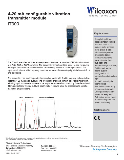
transmitter module iT300The iT300 transmitter provides an easy means to connect a standard IEPE vibration sensor to a PLC, DCS or SCADA system. The transmitter’s input provides power to and measures the signal from either an accelerometer, piezovelocity sensor or dual output sensor. Theinput circuitry has a wide frequency response, capable of measuring signals between 0.2 Hz and 20,000 Hz.The transmitter has two independent processing bands with flexible mapping options to two separate 4-20 mA analog outputs. The processing channels contain selectable integration, allowing input from accelerometers to be output as acceleration or velocity. Selectable band filters and detector types (i.e. RMS, peak) make it easy to tailor the processing to specific machines or applications.Wilcoxon Sensing TechnologiesNote: Due to continuous process improvement, specifications are subject to change without notice.This document is cleared for public release.Band 1 (adjustable)Band 2 (adjustable)transmitter module iT300Wilcoxon Sensing TechnologiesNote: Due to continuous process improvement, specifications are subject to change without notice.This document is cleared for public release.4-20 mA configurable vibration transmitter module iT300System architectureWilcoxon Sensing TechnologiesPower input 4-20 mA outputsInput/output µprocessor00iT300 built-in web server – user-configurableLogin required before anychanges can be madeUser entry of machine indentityUser entry of sensorparametersUser selection of frequencyanalysis rangeAnalysis band type andfrequency limitsMeasurement results4-20 mA mappingDefault configuration. Consultfull manual on configuring yourPC network adaptorDefault user: userDefault password: adminRemember to save your。
两线制4-20mA变送器的电路设计

两线制4/20mA变送器的电路设计工业上普遍需要测量各类非电物理量,例如温度、压力、速度、角度等,都需要转换成模拟量电信号才能传输到几百米外的控制室或显示设备上。
这种将物理量转换成电信号的设备称为变送器。
工业上最广泛采用的是用4~20mA电流来传输模拟量。
采用电流信号的原因是不容易受干扰。
并且电流源内阻无穷大,导线电阻串联在回路中不影响精度,在普通双绞线上可以传输数百米。
上限取20mA是因为防爆的要求:20mA的电流通断引起的火花能量不足以引燃瓦斯。
下限没有取0mA的原因是为了能检测断线:正常工作时不会低于4mA,当传输线因故障断路,环路电流降为0。
常取2mA作为断线报警值。
电流型变送器将物理量转换成4~20mA电流输出,必然要有外电源为其供电。
最典型的是变送器需要两根电源线,加上两根电流输出线,总共要接4根线,称之为四线制变送器。
当然,电流输出可以与电源公用一根线(公用VCC或者GND),可节省一根线,称之为三线制变送器。
其实大家可能注意到, 4-20mA电流本身就可以为变送器供电,如图1C所示。
变送器在电路中相当于一个特殊的负载,特殊之处在于变送器的耗电电流在4~20mA之间根据传感器输出而变化。
显示仪表只需要串在电路中即可。
这种变送器只需外接2根线,因而被称为两线制变送器。
工业电流环标准下限为4mA,因此只要在量程范围内,变送器至少有4mA供电。
这使得两线制传感器的设计成为可能。
在工业应用中,测量点一般在现场,而显示设备或者控制设备一般都在控制室或控制柜上。
两者之间距离可能数十至数百米。
按一百米距离计算,省去2根导线意味着成本降低近百元!因此在应用中两线制传感器必然是首选。
2.两线制变送器的结构与原理 两线制变送器的原理是利用了4~20mA信号为自身提供电能。
如果变送器自身耗电大于4mA,那么将不可能输出下限4mA值。
因此一般要求两线制变送器自身耗电(包括传感器在内的全部电路)不大于3.5mA。
一种双模式氨气传感器的设计与实现
一种双模式氨气传感器的设计与实现徐光;赵全;马德常;许宏【摘要】针对传统氨气传感器使用有线供电及信号传输的局限性,设计了一种双模式氨气传感器.介绍了传感器的工作原理,设计了以MSP430AFE253微处理器为核心的硬件电路,有线供电部分基于AD5420芯片设计,可实现4~20 mA信号输出;无线部分基于ZM5161-P1型无线模块设计,采用Zigbee通信协议进行无线数据传输,电路在软硬件上进行了低功耗设计;传感器可实现工作模式自动切换,对传感器进行了无线通讯距离测试及标准气测试,试验结果表明该传感器可实现工作模式自动切换并具备测量精度高、传输距离远等特点.【期刊名称】《仪表技术与传感器》【年(卷),期】2019(000)006【总页数】4页(P15-18)【关键词】氨气传感器;双模式;4~20mA;ZigBee【作者】徐光;赵全;马德常;许宏【作者单位】北京航天试验技术研究所,北京 100074;北京航天试验技术研究所,北京 100074;北京航天凯恩化工科技有限公司,北京 100074;北京航天试验技术研究所,北京 100074【正文语种】中文【中图分类】TP2160 引言氨作为一种重要的化工原料,在化肥、制冷剂、有机合成等工业都有着广泛的应用,氨气为有毒气体,在对液氨的存储、运输、使用和生产过程中,若发生泄漏情况,会对人员造成中毒伤害且有可能发生爆炸事故。
因此需要对氨在生产、存储、运输等过程进行泄漏监测,以保障人员和设备安全,目前市场上主要使用固定式氨气检测探头对其进行在线监测,固定式探头需要布置电缆进行供电及信号传输,当供电端出现故障或需要进行移动中检测时无法满足使用要求。
本文设计了一种双模式氨气传感器,可采用电缆供电及电池供电2种方式,当电缆供电方式未启用或故障时传感器自动切换至电池供电并通过无线发送数据,可以满足不同工况条件下的氨气泄漏监测需求。
1 传感器组成结构及原理双模传感器由电源模块、电化学传感器、信号处理模块、4~20 mA环路电流发生模块、ZigBee无线发射模块、MSP430AFE253微控制器组成。
基于ZSSC3008的智能应变式传感器设计
基于ZSSC3008的智能应变式传感器设计缪晓中;彭力【摘要】针对压阻式传感器存在的零点偏差、满度偏差以及输出信号的非线性误差,提出了采用ZSSC3008传感器信号调理芯片进行补偿校准的方案;描述了传感器补偿系统的整体构架,阐述了ZSSC3008的硬件结构、应用电路设计以及对传感器的补偿过程;实验结果表明:用上位机补偿校准软件对传感器补偿后,实现了传感器的一致性以及输出信号与压力良好的线性关系,并具有操作效率高的优点.【期刊名称】《计算机测量与控制》【年(卷),期】2015(023)003【总页数】4页(P1065-1068)【关键词】ZSSC3008;应变式传感器;补偿;智能化传感器;XTR117【作者】缪晓中;彭力【作者单位】无锡职业技术学院电子与信息系,江苏无锡 214121;江南大学物联网工程学院,江苏无锡214121【正文语种】中文【中图分类】TP2160 引言智能化与集成化是传感器未来发展的一个重要方向。
将普通传感器与专用信号调理芯片组装成一个器件实现一体化的设计,使之具有对信号的采集、变换、逻辑判断、计算能力,提供数字或模拟输出选择,有与微型计算机通信的接口,有在线标定与校准等功能。
这类智能化传感器在压阻式传感器中应用较多,国外企业在精度、制作成本、芯片体积等方面有较大优势。
德国ZMDI公司的ZSSC3008传感器信号调理芯片,能很方便地实现电阻性桥式传感器的零偏、增益系数等参数的数字化校准。
在Windows环境下芯片通过ZACwire串行接口与上位机相联,可以方便地实现大规模的校准操作。
1 应变式传感器的桥式测量电阻应变式传感器的基本原理是将被测量的变化转换成电阻的变化,再经过转换电路变成电信号输出。
将电阻应变片粘贴在被测试件表面,在外力作用下,被测试件表面产生微小机械变形,应变片亦发生相同变化,其电阻也发生相应变化,而根据应力—应变关系σ =Eε就可以得到试件应力的大小。
测量时通常将敏感元件粘贴在弹性体上组成惠斯登电桥,把待测的非电量变化转换成桥路的电压变化。
什么是变送器的二线制和四线制信号传输方式
一、什么是变送器的二线制和四线制信号传输方式? 二线制传输方式中,供电电源、负载电阻、变送器是串联的,即二根导线同时传送变送器所需的电源和输出电流信号,目前大多数变送器均为二线制变送器;四线制方式中,供电电源、负载电阻是分别与变送器相连的,即供电电源和变送器输出信号分别用二根导线传输。
......请看变送器八问八答。
二.什么是两线制电流变送器? 什么是两线制?两线制有什么优点? 两线制是指现场变送器与控制室仪表联系仅用两根导线,这两根线既是电源线,又是信号线。
两线制与三线制(一根正电源线,两根信号线,其中一根共GND) 和四线制(两根正负电源线,两根信号线,其中一根GND)相比,两线制的优点是: 1、不易受寄生热电偶和沿电线电阻压降和温漂的影响,可用非常便宜的更细的导线;可节省大量电缆线和安装费用; 2、在电流源输出电阻足够大时,经磁场耦合感应到导线环路内的电压,不会产生显著影响,因为干扰源引起的电流极小,一般利用双绞线就能降低干扰;两线制与三线制必须用屏蔽线,屏蔽线的屏蔽层要妥善接地。
3、电容性干扰会导致接收器电阻有关误差,对于4~20mA两线制环路,接收器电阻通常为250Ω(取样Uout=1~5V)这个电阻小到不足以产生显著误差,因此,可以允许的电线长度比电压遥测系统更长更远; 4、各个单台示读装置或记录装置可以在电线长度不等的不同通道间进行换接,不因电线长度的不等而造成精度的差异,实现分散采集,分散式采集的好处就是:分散采集,集中控制.... 5、将4mA用于零电平,使判断开路与短路或传感器损坏(0mA状态)十分方便。
6,在两线输出口非常容易增设一两只防雷防浪涌器件,有利于安全防雷防爆。
三线制和四线制变送器均不具上述优点即将被两线制变送器所取代,从国外的行业动态及变送器心片供求量即可略知一斑,电流变送器在使用时要安装在现场设备的动力线上,而以单片机为核心的监测系统则位于较远离设备现场的监控室里,两者一般相距几十到几百米甚至更远。
- 1、下载文档前请自行甄别文档内容的完整性,平台不提供额外的编辑、内容补充、找答案等附加服务。
- 2、"仅部分预览"的文档,不可在线预览部分如存在完整性等问题,可反馈申请退款(可完整预览的文档不适用该条件!)。
- 3、如文档侵犯您的权益,请联系客服反馈,我们会尽快为您处理(人工客服工作时间:9:00-18:30)。
Circuit Note4 mA-to-20 mA Loop-Powered Temperature Monitor Using theADuC7060/ADuC7061 Precision Analog MicrocontrollerRev. 0“Circuits from the Lab” from Analog Devices have been designed and built by Analog Devices engineers. Standard engineering practices have been employed in the design and construction of each circuit, and their function and performance have been tested and verified in a lab environment at room temperature. However , you are solely responsible for testing the circuit and determining its suitability and applicability for your use and application. Accordingly , in no event shall Analog Devices be liable for direct, indirect, special, incidental, consequential or punitive damages due to any cause whatsoever connected to the use of any “Circuit from the Lab”. (Continued on last page)One Technology Way, P.O. Box 9106, Norwood, MA 02062-9106, U.S.A. Tel: 781.329.4700 Fax: 781.461.3113 ©2010 Analog Devices, Inc. All rights reserved.CIRCUIT FUNCTION AND BENEFITSThis circuit provides a simple highly integrated temperature monitor solution that can interface to a 4 mA-to-20 mA host controller. This circuit provides a very low cost solution to temperature monitoring because so much of the circuit functionality is integrated on the ADuC7060/ADuC7061 precision analog microcontroller, including dual 24-bit Σ-Δ ADCs, the ARM7 processor core, and the DAC/PWM features for controlling the 4 mA-to-20 mA feedback circuit. The performance of the ADCs and other analog circuits within the ADuC7060/ADuC7061 is superior to competitivemicrocontrollers that have integrated analog circuits. Thecircuit presented here represents the most cost-effective, lowest power, lowest board area solution compared to using discrete ADCs and a separate microcontroller. Because of its high level of integration and low power, the ADuC7060/ADuC7061 can operate directly from the loop power in the 4 mA-to-20 mA application. With the ARM7 core running at 640 kHz, theprimary ADC active and measuring the external RTD tempera-ture sensor, and the PWM controlling the 4 mA-to-20 mA feedback circuit, the entire circuit typically consumes 3.15 mA. Further details on the power consumption are provided in the Circuit Description section.R RTD08836-001Figure 1. ADuC7061 Controlling 4 mA-to-20 mA Loop-Based Temperature Monitor Circuit. (Simplified Schematic: All Connections and Decoupling Not Shown)Rev. 0 | Page 2 of 4During the intervals between temperature measurements, the ADC and the RTD excitation current sources can be turned off to further reduce power.The 100 Ω Pt RTD is an Enercorp #PCS11503.1. The complete circuit meets a better than ±1°C specification. The temperature range of this RTD is −50°C to +130°C. The RTD is available in a 1206 size SMD package and has a temperature coefficient of 0.385 Ω/°C.The primary ADC within the ADuC7060/ADuC7061 has a peak-to-peak noise-free code resolution of greater than 18 bits. The PWM based DAC output provides 12 effective bits of resolution. The performance of the overall circuit is discussed in the Circuit Description section.Due to the small form factor of the ADuC7061, a 5 mm × 5 mm 32-LFCSP package, the entire circuit will fit on an extremely small PCB thus further reducing cost.The focus here is primarily the 4 mA-to-20 mA interface aspect of the circuit. For details on the RTD sensor interface to the ADC and on linearization techniques of the RTD measurements, see Application Note AN-0970 and Circuit Note CN-0075.CIRCUIT DESCRIPTIONThe circuit is powered via the ADP1720 linear regulator(adjustable version), which regulates the Loop+ supply to 2.5 V for the ADuC7060/ADuC706161, the OP193 op amp, and the optional ADR280 reference.The 4 mA-20 mA feedback circuit is primarily controlled by the ADuC7060’s on-chip 16-bit PWM (pulse width modulator). The duty cycle of the PWM is configured in software to control the voltage across the 47.5 Ω R LOOP resistor, which in turn sets the loop current. Note the top of R LOOP connects to theADuC7060 ground. The bottom of R LOOP connects to the loop ground. Because of this, the current due to the ADuC7060/ ADuC7061, ADP1720, ADR280, and OP193, plus the current set by the filtered PWM output, flows across R LOOP .V REF is supplied by the ADR280, a 1.2 V precision reference. Alternatively, the on-chip DAC of the ADuC7060/ADuC7061 could be configured to provide the 1.2 V reference, but this would consume extra power by enabling the internal DAC. The voltage at the junction of R1 and R2 can be expressed:V R12 = (V RLOOP + V REF ) × R2/(R1 + R2) – V RLOOP After the loop settles:V IN = V R12 Since R1 = R2:V IN = (V RLOOP + V REF )/2 – V RLOOP = V REF /2 – V RLOOP /2 V RLOOP = V REF – 2V INFull-scale current will flow when V IN = 0, at which point V RLOOP = V REF . Hence, full-scale current is V REF /R LOOP , or ≈24 mA. When V IN = V REF /2, no current will flow.The OP193 amplifier impedance at V IN is high and will not load the PWM filtered output. The amplifier output varies only a small amount around 0.7 V .Performance at the range extremes, 0 mA to 4 mA, and 20 mA to 24 mA, is not critical; therefore, the op amp does not require good performance at the supply rails.Absolute values of R1 and R2 are not critical. However, note that matching of R1 and R2 is important.Also note the possibility of measuring the voltage at the point marked V R12 by using an input channel of ADC0 on the ADuC7060/ADuC7061. This ADC measurement can be used as feedback for the PWM control software to adjust the 4 mA-to-20 mA current setting.The primary ADC of the ADuC7060/ADuC7061 measures the voltage across the RTD. The RTD is excited by the on-chip excitation current source, IEXC0. It is recommended that the excitation current is configured for 200 µA to conserve power, and it should be switched off between measurements. Theinternal PGA on the front end of the primary ADC is configured for either a gain of 16 or 32. The reference source for the RTD measurement may be either the internal reference or the exter-nal 5.62 kΩ reference resistor. Selecting the external resistor will conserve further power. For further details on the RTD to ADC interface and on linearization techniques for the ADC results see Application Note AN-0970 and Circuit Note CN-0075. Power requirements for the circuit depend on whether the module is powered directly from the 4 mA-to-20 mA loop supply or actively from a 4-wire loop where the module is powered separately. For this document, we will assume the temperature monitor module is loop powered, therefore the total current consumption of the module should not exceed approximately 3.6 mA.To facilitate low power operation, the ADuC7060/ADuC7061 core operating speed can be reduced by programming the internal POWCON0 register. This allows the top frequency of 10.28 MHz to be divided in binary multiples of 2 to 128. During the tests, a clock divide value of 16 was used, giving a core speed of 640 kHz. The primary ADC was enabled with a gain of 32. The PWM was also enabled. All other peripherals were disabled.For our circuit and test setup, Table 1 gives a breakdown of the I DD current consumption, and Table 2 gives the currents for the various peripherals.Rev. 0 | Page 3 of 4Table 1. Typical I DD Values for Components of TemperatureThe DNL graph in Figure 2 shows a better than 0.6 LSB typical performance in the critical 4 mA-to-20 mA range. These tests were conducted with a second order filter on the PWM output. Two 47 kΩ resistors and two 100 nF capacitors were used as shown in Figure 1.LOOP CURRENT (µA)DNL (LSBs)8836-002Figure 2. Typical DNL performance of circuitThe performance of the PWM based output could be enhanced by using the ADC to measure the voltage point V R12 and other points on the circuit. This method of feedback could be used to calibrate the PWM output for greater precision.Note that the PWM circuit was only used to set the output voltage between 0 V and 600 mV , hence the reduced number of codes. Code 0 above is not important as it represents a value greater than 24 mA.For ADC measurement performance, see AN-970 and CN-0075 and the ADuC7060/ADuC7061 data sheet .Table 2. Typical I DD Values for Different Peripherals on the COMMON VARIATIONSInstead of using the PWM, the on-chip DAC could be used for the same function. The advantage would be quicker response time and a cheaper solution. The ADR280 reference would not be required in this case.The OP90 can be used instead of the OP193.LEARN MOREADIsimPower Design Tool, Analog Devices.CN-0075 Circuit Note, USB Based Temperature Monitor Usingthe ADuC7061 Precision Analog Microcontroller and an External RTD . Analog Devices.Kester, Walt. Sensor Signal Conditioning , Analog Devices, 1999,Chapter 7, Temperature Sensors . Kester, Walt. Sensor Signal Conditioni ng, Analog Devices, 1999,Chapter 8, ADCs for Signal Conditioning . Looney, Mike. AN-0970 Application Note, RTD Interfacing andLinearization Using an ADuC706x Microcontroller , Analog Devices. MT-022 Tutorial, ADC Architectures III: Sigma-Delta ADCBasics , Analog Devices. MT-023 Tutorial, ADC Architectures IV: Sigma-Delta ADCAdvanced Concepts and Applications , Analog Devices. MT-031 Tutorial, Grounding Data Converters and Solving theMystery of "AGND" and "DGND", Analog Devices. MT-101 Tutorial, Decoupling Techniques , Analog Devices.Rev. 0 | Page 4 of 4Data Sheets and Evaluation Boards ADP1720 Data Sheet ADR280 Data Sheet ADuC7060 Data SheetADuC7060 Evaluation Board and Software ADuC7061 Data SheetADuC7061 Evaluation Board and Software OP193 Data Sheet OP293 Data Sheet OP90 Data SheetREVISION HISTORY2/10—Revision 0: Initial Version(Continued from first page) "Circuits from the Lab" are intended only for use with Analog Devices products and are the intellectual property of Analog Devices or its licensors. While you may use the "Circuits from the Lab" in the design of your product, no other license is granted by implication or otherwise under any patents or other intellectual property by application or use of the "Circuits from the Lab". Information furnished by Analog Devices is believed to be accurate and reliable. However, "Circuits from the Lab" are supplied "as is" and without warranties of any kind, express, implied, or statutory including, but not limited to, any implied warranty of merchantability, noninfringement or fitness for a particular purpose and no responsibility is assumed by Analog Devices for their use, nor for any infringements of patents or other rights of third parties that may result from their use. Analog Devices reserves the right to change any "Circuits from the Lab" at any time without notice, but is under no obligation to do so. Trademarks and registered trademarks are the property of their respective owners.©2010 Analog Devices, Inc. All rights reserved. Trademarks and registered trademarks are the property of their respective owners.CN08836-0-2/10(0)。