EM4095中文资料
409CNQ150中文资料
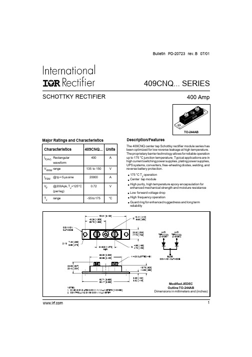
The 409CNQ center tap Schottky rectifier module series has been optimized for low reverse leakage at high temperature.The proprietary barrier technology allows for reliable operation up to 175 °C junction temperature. Typical applications are in high current switching power supplies, plating power supplies,UPS systems, converters, free-wheeling diodes, welding, and reverse battery protection.175 °C T J operation Center tap moduleHigh purity, high temperature epoxy encapsulation for enhanced mechanical strength and moisture resistance Low forward voltage drop High frequency operationGuard ring for enhanced ruggedness and long termreliabilityDescription/FeaturesMajor Ratings and Characteristics I F(AV)Rectangular400A waveform V RRM range135 to 150V I FSM @ tp = 5 µs sine 20000A V F @ 200Apk, T J =125°C 0.72V(per l eg)T Jrange- 55 t o 175°CCharacteristics409CNQ...UnitsSCHOTTKY RECTIFIER409CNQ... SERIES400 AmpBulletin PD-20723 rev. B 07/01TO-244AB409CNQ... Series2Part number409CNQ135409CNQ150V RMax. DC Reverse Voltage (V)V RWM Max. Working Peak Reverse Voltage (V)135150Voltage RatingsAbsolute Maximum RatingsFollowing any rated load condition and withrated V RRM applied Parameters409CNQ Units C onditionsA I F(AV)Max. A verage F orward C urrent (Per l eg)200A50% d uty c ycle @T C =125 °C, r ectangular w ave f orm* See Fig. 5(Per d evice )400I FSM Max. P eak O ne C ycle N on-Repetitive200005µs S ine o r 3µs R ect. p ulse Surge C urrent (Per L eg) *S ee F ig. 7230010ms Sine or 6ms Rect. pulse E AS Non-Repetitive A valanche E nergy15mJ T J = 25 °C, I AS = 1 Amps, L = 30 mH(Per L eg)I ARRepetitive A valanche C urrent 1ACurrent decaying linearly to zero in 1 µsec(Per L eg)Frequency limited by T J max. V A = 1.5 x V R typical (1) Pulse Width < 300µs, Duty Cycle <2%T J Max. J unction T emperature R ange - 55 t o 175°C T stgMax. S torage T emperature R ange- 55 t o 175°CR thJC Max. T hermal R esistance J unction0.20°C/W DC o peration * See Fig. 4to C ase (Per L eg)R thJC Max. T hermal R esistance J unction0.10°C/W DC o perationto C ase (Per P ackage)R thCS Typical T hermal R esistance, C ase0.10°C/W Mounting s urface ,s mooth a nd g reased to H eatsink wt Approximate W eight 79 (2.80)g (oz.)TMounting T orque B ase Min.24 (20)Max.35 (30)Mounting T orque C enter H oleTyp.13.5 (12)Terminal T orque Min.35 (30)Max.46 (40)Case S tyleTO - 244AB Modified J EDECThermal-Mechanical SpecificationsParameters409CNQ Units C onditionsV FMMax. Forward Voltage Drop 1.03V @ 200A (Per Leg) * See Fig. 1(1)1.21V @ 400A 0.72V @ 200A 0.83V @ 400A I RM Max. Reverse Leakage Current 6mA T J = 25 °C (Per Leg) * See Fig. 2(1)85mA T J = 125 °CC T Max. Junction Capacitance (Per Leg)6000pF V R = 5V DC , (test signal range 100Khz to 1Mhz) 25°C L STypical Series Inductance(Per Leg)5.0nH From top of terminal hole to mounting planedv/dt Max. Voltage Rate of Change10000V/ µs(Rated V R )T J = 25 °C T J = 125 °C V R = rated V RParameters409CNQ UnitsConditionsKg-cm(Ibf-in)Electrical Specifications409CNQ... Series3409CNQ... Series4FREE-W HEELD IO D E40HFL40S02C URRE NTM O N ITO RH IG H-SPEEDSW ITC HIRFP460LD UTRg = 25 ohm V d = 25 Volt+Average F orward C urrent -IF (AV)(A)Square W ave P ulse D uration -tp(microsec)Fig. 7 - Max. Non-Repetitive Surge CurrentAllowableCaseTemperature(°C)Non-RepetitiveSurgeCurrent-IFSM(A)Fig. 6-F orwardP ower L oss C haracteristicsAverage F orward C urrent -IF (AV)(A)AveragePowerLoss(Watts)Fig. 8-U nclamped I nductive T est C ircuit(2)Formula used: TC = TJ- (Pd + PdREV) x RthJC;Pd = Forward Power Loss = IF(AV) x VFM@ (IF(AV)/ D) (see Fig. 6);PdREV = Inverse Power Loss = VR1x IR(1 - D); IR@ VR1= rated VR4080120160200050100150200250300 100010000100000101001000100006080100120140160180050100150200250300409CNQ... Series5Bulletin PD-20723 rev. A 07/01 IR WORLD HEADQUARTERS: 233 Kansas St., El Segundo, California 90245, USA Tel: (310) 252-7105TAC Fax: (310) 252-7309Visit us at for sales contact information. 07/01Data and specifications subject to change without notice.This product has been designed and qualified for Industrial Level.Qualification Standards can be found on IR's Web site.。
LTC4095中文规格书
参数
条件
再充电比较器反应时间
BAT 下降中
充电定时器截止周期 失效电池截止时间 充电结束时指示器电流水平Current Level
BAT = VFLOAT BAT < VTRKL (Note 5)
充电结束时比较起反应时间
电池充电器 Power FET 导通电阻 (在IN与BAT之间)
IBAT 下降中 IBAT = 200mA
Differential Undervoltage Lockout Threshold
Differential Undervoltage Lockout Hysteresis PROG 引脚的比较反馈电压
hPROG ITRKL VTRKL ΔVTRKL ΔVRECHRG
Ratio of IBAT to PROG Pin Current 涓流充电电流 涓流充电截止电压 涓流充电迟滞电压 电池再充电门限电压
恒定温度下的最高结温
最小值
3.5 0.4375 0.09
典型值 1.7 4 0.5 0.1 2.2 500
最大值
4.5 0.5625 0.11
单位 ms Hour Hour mA/mA ms mΩ
115
°C
NTC VCOLD VHOT VDIS
ห้องสมุดไป่ตู้
过冷温度错误截止电压 过热温度错误截止电压 NTC失效截止电压
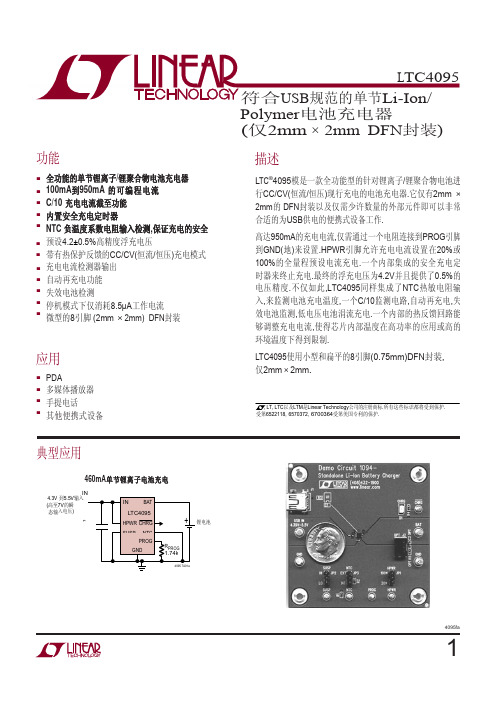
Note 2: The LTC4095 is guaranteed to meet performance specifications from 0°C to 85°C. Specifications over the –40°C to 85°C operating temperature range are assured by design, characterization and correlation with statistical process controls.
焦炉大车联锁技术
焦炉大车联锁技术2006-11-17 13:56:00北京三博供稿一.前言随着现代科技的不断发展,新的技术成果被越来越多的应用在工业过程监视控制领域,在焦化行业也是如此,但是由于生产工艺的特殊性,使自动化技术在焦化行业,特别是在焦炉生产过程的监视和控制尤其困难,比如焦炉加热自动控制、焦炉三车联锁和焦饼测温等等。
二.控制难点实现三车联锁监控系统主要解决两个问题,即数据的传输和各车辆炉号识别。
本系统采用无线数传电台进行数据传输,该方式具有安装调试方便、投资和维护费用小、使用安全可靠等优点,随着国内外无线通讯技术的成熟和不断发展,采用无线数传电台进行数据通讯越来越快,可靠性也很高,因此这种技术已被多数焦化厂所认认同。
另外本系统采用绝对编码板和条码结合的双保险方式进行炉号识别,通过激光识别炭化室绝对编码地址及条码相对位移的位置识别技术,确保准确识别炉号。
在本系统中自动包含推焦电流记录功能。
该功能是全国炼焦行业协会提出焦炉自动化“四项技术”中的一项,对加强焦炉推焦操作管理,提高焦炉作业水平,保护炉体,实现焦炉预检预修,延长焦炉使用寿命具有重要作用。
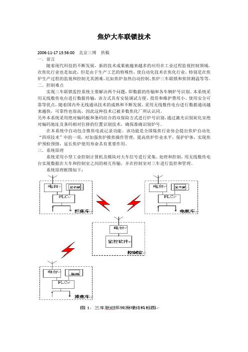
三.系统原理系统采用小型工业控制计算机及模块对大车信号进行采集、处理和控制,用无线数传电台实现数据在大车和控制室之间的相互传输,并在控制室对三车进行监控和管理。
系统原理框图如下:具体原理描述1、焦炉三大车使用工业级可编程控制器(PLC)作为信号输入输出、计算、控制、通讯和显示的核心部分;2、各车辆采用激光测量仪及条码定位技术识别炉号;3、各车辆之间以及各车辆与控制室之间采用无线数字电台进行通讯;4、上位机使用工业PC机和专门开发的“三车联锁监控管理软件”进行控制和管理功能;四、系统结构组成1、每套焦炉主站及从站设置主站:1个,设置在控制室中;从站:3个,三大车上(包括推焦车、拦焦车、电机车各一辆)每车一个从站。
(根据车辆数量情况,从站数量可能有所变化。
)焦炉主站及各从站组成见下图。
EM4094中文资料

EM4094Copyright 2003, EM Microelectronic-Marin SA Subject to change without noticeRev. A, 09/03Phone: +41.32.755-5111, Fax: +41.32.755-5403info@Analog Front End Integrated Circuit for13.56MHz RFID Base StationGeneral DescriptionThe EM4094 is an integrated analog system for 13.56MHz RFID reader system. It is highly versatile so it can be used in different reader systems havingsub-carrier frequencies from 212KHz to 848KHz, hence covering ISO 14443 and ISO 15693 standards.The adaptability is achieved using a 3 wires serial interface to program the system option bits.The transmitter generates 200 mW output power into 50Ω load and is capable of OOK or ASK modulation.ApplicationsLow cost reader solutionHand held readerFeaturesISO 15693 & ISO14443 compatibilityOscillator using 13.56MHz Quartz with selectable transconductance (gm).Antenna driver using OOK or ASK modulation usingsingle antenna driverASK modulation adjustable in range from 7% to 30% High output power 200mW from 5V supply Antenna short circuit protectionMultiple receiver input for high communicationreliabilityAM/PM demodulation with AGC signal amplifier 848KHz BPSK internal decoder (type B) Multiple sub-carrier receiving compatibility (212kHz, 424kHz and 848kHz)Multiple sub-carrier coding compatibility (Manchester, BPSK)Built-in receive low-pass filter cut-off frequencyselectable between 400kHz and 1MHzBuilt-in receive high-pass filter cut-off frequencyselectable between 100kHz, 200kHz and 300kHz Selectable receive gainSerial 3 pin interface for option selectionPower down mode controlled by the 3 wires SPI Output Power: 200mW for a SO20w Package100mW for a SO16w PackageOperation temperature range -40°C to +85°CTypical ApplicationFigure 1EM MICROELECTRONIC- MARIN SA元器件交易网。
em4095
/************************************************
*函数 :InitQ()
*调用函数:
*参数:
*功能描述: em4095系统初始化接收缓冲区
by:
**************************************************/
/************************************************
*函数 :DelayMs()
*调用函数:
*参数:
*功能描述: em4095延时子程序X*ms
by:
**************************************************/
* 输入 : 无
* 输出 : 无
***********************************************************************/
void delay()
{
int i,j;
for(i=0; i<=10; i++)
for(j=0; j<=2; j++)
L1602_string(1,5,"ab cd ef;")
* 输入 : 行,列,需要输入1602的数据
* 输出 : 无
***********************************************************************/
void L1602_string(uchar hang,uchar lie,uchar *p)
RFID开发技术及实践 第4章
4.1.3 EM4100解码 对EM4100进行解码时,判断一帧完整数据的开始,需
要判断同步头,因为数据中的行列校验会保证数据中不会连 续出现9个1。由于只要在阅读器范围内,EM4100就会循环 送出内部的64bit数据,并且最后一个停止位为数据0。因此 判断同步头的方法是当第一次读取数据时,遇到0至1的跳变 开始计数,如果读到连续9个1,则为同步头,从同步头往后 可依次读取剩余的bit位。
3. 锁相环 锁相环由环路滤波、采样器和比较模块等组成。通过使 用外部电容分压,DEMOD_IN引脚上得到天线上真实的高 电压。这个信号的相位和驱动天线驱动器信号的相位进行比 较。所以锁相环可以将载波频率锁定在天线的谐振频率上。 根据天线种类的不同,系统的谐振频率可以在100~150 kHz的范围内。当谐振频率在这一范围内的时候,它就会被 锁相环锁定。
描述 电源地 就绪标志和时钟输出,AM 调幅驱动 天线驱动 天线驱动正电源 天线驱动负电源 天线驱动 正电源 天线探测电压 DC 电容输出 DC 电容输入 模拟地 天线高电平调制 数字解调数据输出 高电平驱动电流进入休眠态 PLL 滤波电容 DC 去耦电容
类型 地
输出 输出 电源
地 输出 电源 模拟信号 模拟信号 模拟信号 模拟信号 上拉输入 输出 上拉输入 模拟信号 模拟信号
第4章 低频RFID阅读器设计
4.1 低频ID卡 4.2 EM4095 4.3 低频RFID阅读器程序设计
4.1 低频ID卡
低频RFID由于频率较低,带宽有限,所以不适合传输 大量数据以及数据写入。因此低频RFID标签通常是以ID卡 的形式出现,即在标签中固化一串ID号,阅读器仅可以阅 读,不能写入和更改。
图4-4 原理图
2. MOD 引脚MOD是用来对125 kHz射频信号进行调制的,其功 能如下: 在MOD引脚上施加高电平时,会阻塞天线驱动,并 关掉电磁场。 在MOD引脚上施加低电平时,会使片上VCO进入自 由运行模式,天线上将出现没有经过调制的125 kHz的载波。 EM4095用作只读模式,引脚MOD没有使用,推荐将它 连接至VSS。
Omega PX409 RS485序列压力传感器说明书

RS485 Output Silicon Pressure TransmitterDigital RS485 with Analog Output Imperial and MetricPX409-485/PXM409-485SeriesGage and Absolute Pressures10 inH 20 to 5000 psi (25 mb to 345 bar) Vacuum and Compound Ranges 10 inH 20 to 15 psi (25 mb to 1 bar)Barometric Pressure Ranges0 to 32, 16 to 32, and 26 to 32 inHg (0 to 1100 hPa, 550 to 1100 hPa, and 880 to 1100 hPa)The PX409 RS485 Series is an industrial RS485 silicon pressure sensor. Use as a stand-alone for up to 640 Hz sampling rate, or connect up to 16 units in an independent multidrop RS485 network at 1 Hz overall bus sampling rate. Interface to the sensor using command line access, or use the free PC software from OMEGA to chart, log, display, and output data for analysis. An additional analog output (0 to 5V , or 4 to 20 mA) provides even more flexibility. The micro-machined silicon design isideal for pressure or level applications in laboratory, test platforms, or bio/pharmaceutical applications as well as industrial applications that require arugged, high accuracy transmitter that can transmit over long distances. The micro-machined silicon sensor provides a very stable transmitter with exceptional high accuracy of ±0.08% and a broad compensated range of -29 to 85°C (-20 to 185°F). The modular construction allows for fast delivery ofmost configurations and fittings.U U p to 640 Readings/Second U M icro-Machined Silicon SensorU 316L SS Wetted PartsU High ±0.08% BSL Accuracy U RS485 and Analog Outputs U E xcellent Long Term Stability U M12 Connection U R uggedized with Secondary ContainmentPX459-485/PXM459-485, shown smaller than actual size.SpecificationsSupply: 12 to 36 Vdc (when using mA output, derate using formula in operating temperature section) Maximum Loop Ω: (Supply-9) x 50Accuracy: 0.08% BSL (linearity, hysteresis and repeatability combined)Resolution: Up to 5.5 significant figuresZero Balance: ±0.5% FS typical 1% maximum (1% typical, 2% maximum for 2.5 psi and below)Span Setting: ±0.5% FS typical 1% maximum (1% typical, 2% maximum for 2.5 psi and below). Calibrated in vertical direction with fitting downTemperature Compensation (Over Compensated Range): Span: Range > 5 psi: ±0.5%; Range ≤ 5 psi: ±1.0% Zero: Range > 5 psi: ±0.5%; Range ≤ 5 psi: ±1.0%Minimum Isolation: 100 M Ω @ 50 Vdc case to sensor, 2 M Ω @ 50 Vdc case to output terminations Pressure Cycles: 1 million, minimumLong Term Stability (1-Year): ±0.1% full scale typical Power Consumption: -5V: 0.65 W typical -I: 1.25 W maximumCompensated Temperature Imperial:Ranges >5 psi: -29 to 85°C (-20 to 185°F) Ranges ≤5 psi: -17 to 85°C (0 to 185°F) Metric:Ranges > 350 mb: -29 to 85°C (-20 to 185°F) Ranges ≤ 350 mb: -17 to 85°C (0 to 185°F)Pressure Port:Imperial: ¼–18 NPT male Metric: G-¼ maleA to D Conversion: 24-bitOutput: RS485 digital with discrete analog (choose 0 to 5 Vdc or 4 to 20 mA)DAC Conversion: 320 Hz at 16 bit Bandwidth:Multidrop Mode: Overall Bus rate: DC to 1 update per second typicalStandalone Mode: DC to 640 updates per secondElectrical Termination: 8-pin M12 type A male with shield pin connection (IEC61076-2-101); female M12 connector M12.8-S-F-FM with screw terminals sold separately CE Compliant: Meets industrial EN61326 Emissions, Burst and SurgeSusceptibility (10 V/m): ±0.25% max, all outputs, Tested using 6.1 m (20') shielded 6 conductor cableESD Protection: T ested to 4 kV to case and shielded wire Digital Outputs: Protection device rated to ±13 kV Analog Output: Protection device rated to: Contact: ±8 kV min, ±30 kV max Air: ±15 kV min, ±30 kV maxFor Stated EMC Performance: Use recommended cable, tie drain wire to shield connection on PX409-485 side, and to earth ground on supply side. Ground PX409-485 case Environmental Protection: IP65RS485 (Non-Isolated):Protocol: OMEGA command structure (provided) Unit Load: 1⁄8Standalone and Addressed Multidrop Modes Recommended Cable: Belden 9843 or equivalent Maximum Number of Units on One RS485 Bus: 16 units (multidrop mode), 1 unit (standalone mode) Software-enabled 120Ω termination resistor10 inH 2O to 5 psi: to 1000 psi 15 to 1000 psi: to 3000 psi 1500 to 5000 psi: to 10,000 psi Absolute/Barometric Pressure: 5 to 1000 psia: to 6000 psia1500 to 5000 psia: to 10,000 psia OverpressureGage/Vacuum/Compound Pressure: 10 inH 2O: 10 times span 1 psi: 6 times span2.5 psi to 1000 psi: 4 times span1500 psi to 5000 psi: 7250 psi maximum Absolute/Barometric Pressure: 5 psia: 6 times span15 psia to 1000 psia: 4 times span 1500 to 5000 psia: 7250 psia maximumSecondary ContainmentGage/Vacuum/Compound Pressure:25 to 350 mb: to 70 bar 1 to 70 bar: to 200 bar 100 to 350 bar: to 700 bar Absolute/Barometric Pressure: 350 mb to 70 bar: to 400 bar 100 to 350 bar: to 700 bar OverpressureGage/Vacuum/Compound Pressure: 25 mb: 10 times span 70 mb: 6 times span170 mb to 100 bar: 4 times span 175 to 350 bar: 500 bar maximum Absolute/Barometric Pressure:350 mb to 100 bar Absolute: 4 times span 175 to 350 bar Absolute: 500 bar maximum Wetted Parts: 316L stainless steel Weight: 200 g (7 oz)Operating Temperature Range: -40 to 85°C (-40 to 185°F); when using mA output; maximum ambient temperature = 106 + (0.038) R-(2.1)V where R = Loop Ω and V = VsupplyOrdering Examples: PX459-100G485-5V, 100 psi gage transducer with RS485 and 0 to 5 Vdc outputs, M12 electrical connection, and 1⁄4–18 NPT male pressure port.Mating connector M12.8-S-F-FM (sold separately).PX459-5.0KA485-I, 5000 psi absolute pressure transducer with RS485 and 4 to 20 mA outputs, M12 electrical connection, and 1⁄4–18 NPTmale pressure port.Accessories Comes complete with 5-point NIST -traceable calibration and free downloadable software.Ordering Examples: PXM459-010BG485-5V, 10 bar gage transducer with RS485 and 0 to 5 Vdc outputs, M12 electrical connection, and G-¼ male pressure port.Mating connector M12.8-S-F-FM (sold separately).PXM459-350HA485-I, 350 mbar absolute pressure transducer with RS485 and 4 to 20 mA outputs, M12 electrical connection, and G-¼ male pressure port.。
125KHz非接触式IC卡原理与应用(全)
125KHz非接触式IC卡原理与应用第一部分:基本知识一、简介IC卡(Integrated Circuit Card)经过20多年的发展,已广泛应用于金融、电信、保险、商业、国防、公共事业等领域。
IC卡按外部接口设备的连接方式可分为接触式IC卡和非接触式IC卡(又称射频卡,RFID)两类。
接触式IC卡,就是IC卡与外界进行数据通讯时,芯片的电极触点必须与IC卡读写设备直接连接;非接触式IC卡在使用时则无须与IC卡读写器设备直接连接,而是通过无线电波或电磁感应的方式实现与IC卡读写设备的数据通讯。
在刷卡速度要求高,用卡环境恶劣,污染严重等环境下,非接触式IC卡有着它特有的优势。
非接触式IC卡成功地解决了无源(卡中无电源)和免接触这一难题,是电子器件领域的一大突破,由于其高度安全保密、通信速率高、使用方便、成本日渐低廉等特点而得到广泛使用,主要应用于智能门禁控制、智能门锁、考勤机以及自动收费系统等。
射频卡与接触式IC卡相比有以下优点:●可靠性高,无机械接触,从而避免了各种故障;●操作方便,快捷,使用时没有方向性,各方向操作;●安全和保密性能好,采用双向验证机制。
读写器验证IC卡的合法性,同时IC卡验证读写器的合法性。
每张卡均有唯一的序列号。
制造厂家在产品出厂前已将此序列号固化,不可再更改,因此可以说世界上没有两张完全相同的非接触IC卡。
射频卡根据使用频段的不同可分为低频卡和高频卡、超高频卡:●低频卡与读写器间通信使用的频段为低频段, 常用频点有125kHz、134kHz;●高频卡、超高频卡与读写器间通信使用的频段为高频段, 如13.56MHz、915MHz、2.45GHz等。
按工作距离的不同也可分为近距离卡和远距离卡:●近距离卡与读写器之间的有效作用距离为几厘米到几十厘米以内;●远距离卡与读写器之间的有效作用距离可达一到十几米以上。
按操作类型又可分为:低/高频只读型、低/高频无加密读写型、低/高频可加密读写型、多扇区独立加密应用型以及用户自定义分区应用型等。
集电极带电阻的三极管型号
【字数统计:2952字】一、引言三极管作为一种重要的电子器件,广泛应用于各个领域。
在三极管的分类中,集电极带电阻的三极管具有一定的特殊性。
本文将会对集电极带电阻的三极管进行深入的探讨和评估,以帮助读者全面了解其特点、应用以及未来的发展方向。
二、背景知识在我们深入讨论集电极带电阻的三极管之前,首先我们需要了解一些基础的背景知识。
1. 三极管三极管,也称为双极型晶体管,是一种半导体器件,由发射极、基极和集电极组成。
它具有放大、开关和稳压等多种功能,因此被广泛应用于放大电路、开关电路、稳压电源等各种电子设备中。
2. 集电极带电阻在传统的三极管中,集电极通常是一个无源电极。
然而,为了提高电路的性能和稳定性,人们开始尝试在集电极引入一个带电阻的电极。
这样一来,集电极不仅能够接收电流信号,还能提供一个电阻来控制电路的放大倍数。
三、集电极带电阻的三极管型号在这一部分,我们将对一些常见的集电极带电阻的三极管型号进行介绍,以便读者对其有一个初步的了解。
1. BC546BC546是一种常见的集电极带电阻的三极管型号。
它具有高电压、中电流的特点,适用于低噪声放大、混频器和开关电路等应用中。
该型号具有良好的高频特性和低噪声系数,适合用于广播接收机和电视机等高品质音频和视频信号处理电路。
2. BC547BC547是一款常用的低功耗NPN型三极管,也是集电极带电阻的三极管型号之一。
它具有高电压、低噪声、中电流的特点,广泛应用于各种放大电路、开关电路以及工业控制设备。
3. BC548BC548是另一种常用的集电极带电阻的三极管型号。
它与BC547类似,同样是一种低功耗NPN型三极管,也适用于各种电子设备的放大和开关应用中。
四、集电极带电阻三极管的特点现在我们已经对一些常见的集电极带电阻的三极管型号有了初步的了解,接下来我们将探讨集电极带电阻三极管的一些特点。
1. 高放大倍数集电极带电阻的三极管由于在集电极引入了电阻,使得其在电路中具有更高的放大倍数。
AO4459中文资料

AO4459中⽂资料SymbolTyp Max 33406275R θJL 1824Maximum Junction-to-Lead CSteady-State°C/WThermal Characteristics ParameterUnits Maximum Junction-to-AmbientAt ≤ 10s R θJA °C/W Maximum Junction-to-Ambient ASteady-State °C/W AO4459AO4459SymbolMin TypMaxUnits BV DSS -30V -1T J =55°C-5I GSS ±100nA V GS(th)-1.5-1.85-2.5V I D(ON)-30A 3846T J =125°C53685872m ?g FS 11S V SD -0.78-1V I S-3.5A C iss 668830pF C oss 126pF C rss 92pF R g69?Q g (10V)12.716nC Q g (4.5V) 6.4nC Q gs 2nC Q gd 4nC t D(on)7.7ns t r 6.8ns t D(off)20ns t f 10ns t rr 2230ns Q rr15nCTHIS PRODUCT HAS BEEN DESIGNED AND QUALIFIED FOR THE CONSUMER MARKET. APPLICATIONS OR USES AS CRITICAL COMPONENTS IN LIFE SUPPORT DEVICES OR SYSTEMS ARE NOT AUTHORIZED. AOS DOES NOT ASSUME ANY LIABILITY ARISING OUT OF SUCH APPLICATIONS OR USES OF ITS PRODUCTS. AOS RESERVES THE RIGHT TO IMPROVE PRODUCT DESIGN,FUNCTIONS AND RELIABILITY WITHOUT NOTICE.DYNAMIC PARAMETERS Maximum Body-Diode Continuous CurrentGate resistanceV GS =0V, V DS =0V, f=1MHzV GS =0V, V DS =-15V, f=1MHz Input Capacitance Output Capacitance Turn-On Rise Time Turn-Off DelayTime V GS =-10V, V DS =-15V, R L =2.5?, R GEN =3?Turn-Off Fall TimeTurn-On DelayTime SWITCHING PARAMETERSTotal Gate Charge (4.5V)Gate Source Charge Gate Drain Charge Total Gate Charge (10V)V GS =-10V, V DS =-15V, I D =-6.5Am ?V GS =-4.5V, I D =-5AI S =-1A,V GS =0V V DS =-5V, I D =-6.5AR DS(ON)Static Drain-Source On-ResistanceForward TransconductanceDiode Forward VoltageI DSS µA Gate Threshold Voltage V DS =V GS I D =-250µA V DS =-24V, V GS =0VV DS =0V, V GS =±20V Zero Gate Voltage Drain Current Gate-Body leakage current Electrical Characteristics (T J =25°C unless otherwise noted)STATIC PARAMETERS ParameterConditions Body Diode Reverse Recovery Time Body Diode Reverse Recovery ChargeI F =-6.5A, dI/dt=100A/µsDrain-Source Breakdown Voltage On state drain currentI D =-250µA, V GS =0V V GS =-10V, V DS =-5V V GS =-10V, I D =-6.5AReverse Transfer Capacitance I F =-6.5A, dI/dt=100A/µs A: The value of R θJA is measured with the device mounted on 1in 2FR-4 board with 2oz. Copper, in a still air environment with T A =25°C. The value in any a given application depends on the user's specific board design. The current rating is based on the t ≤ 10s thermal resistance rating.B: Repetitive rating, pulse width limited by junction temperature.C. The R θJA is the sum of the thermal impedence from junction to lead R θJL and lead to ambient.D. The static characteristics in Figures 1 to 6 are obtained using < 300µs pulses, duty cycle 0.5% max.E. These tests are performed with the device mounted on 1 in 2FR-4 board with 2oz. Copper, in a still air environment with T A =25°C. The SOA curve provides a single pulse rating. Rev0 Sept 2006AO4459AO4459。
EM92547D中文资料(ELAN Microelectronics)中文数据手册「EasyDatasheet - 矽搜」
kHz时谐振器. O (环检测器)(低有效),该输出检测到一个有效振铃信号存在
. O (载波检测)(低有效)这个输出表明在带信号在设备输入存在
. O 解调FSK数据输出到该引脚.
电源电压. 非相连.
功能说明
EM92547D
TIP 1
RING 2
环DET1
3
环DET2
4
NC 5
响铃时间
6
PWR UP 7
DVSS 8
ቤተ መጻሕፍቲ ባይዱ
16 VDD 15 SHORTDATA 14 DATA OUT 13 CD 12 RD 11 NC 10 OSCIN 9 OSCOUT
功能框图
Tip Ring
带通 滤器
FSK Demod
数据有效 能源挪威
电路
DATAOUT /CD
环DET1 环DET2 /振铃时间
/PWR UP
Ring
Det.
电路
Power Up
数据重 定时
SHORTDATA /RD
OSCIN OSCOUT
Clock
~2~
芯片中文手册,看全文,戳
EM92547A/B/D 来电显示FSK解调器
引脚说明
符
TIP RING 环DET1 环DET2
特征
兼容Bellcore GR-30-核心(以前为TR-NWT-000030). 兼容与英国电信(BT)SIN227&SIN242. FSK demodulator for Bell 202 and ITU-T V.23 (formerly as CCITT V.23)
134.2K读卡器设计文档
134.2K读卡器模组文档1.工作原理:读卡器采用射频读写芯片EM4095。
EM4095的工作模式是由引脚SHD和MOD的逻辑电平来控制。
当SHD引脚为高电平时,EM4095处于休眠模式。
芯片上电时SHD引脚必须为高电平,以便芯片初始化。
SHD为低电平时,电路发射射频载波,开始解调天线接收到的AM信号,解调的数字信号通过DEMOD OUT 引脚送到微控制器,以便进行解码和处理。
MOD引脚为高电平时电路处于三态,MOD接地使芯片进入只读状态。
EM4095内部集成了锁相环系统,该系统可自适应调整天线谐振频率,发射100~150 kHz的载波,完成读取射频卡信息的工作。
射频卡本身不带电源,是通过负载调制的方式耦合到应用终端的天线上,需要从EM4095发送的射频信号中提取能量,所以在读取射频卡数据时,EM4095要连续发射射频载波信号。
射频卡内有一个LC串联谐振电路,其谐振频率与射频载波频率一致,在电磁波的激励下,LC谐振电路产生共振,从而产生感应电势,当电量累积到一定数量时,就可以作为电源为电路提供工作电压,将卡内信息发送出去。
EM4095通过天线接收射频卡发回的信号,并对接收的信号解调,从而得到射频卡中的信息。
然后把信息发送给单片机,由单片机按照射频卡的无线通信协议对数据解码、保存或者通过串口传给上位机进行处理。
2.硬件组成:EM4095+ STC90C52原理图详见134.2KREADERV1.1PCB图祥见134.2KRFREADERV1.13. 天线调试:f0为谐振频率;动物标签频率为134.2 kHz;L为天线线圈的电感;C为电容并联的总电容值,调试天线为560UH,C4为1.5n/100V,C7为180p/100V,C6为20p/100V,C10为1n/100V;测试 f0为148KHz.通过调节C4,C7根据公式可以调节f0。
通过调节R7可以改变天线电压峰峰值,R7=10欧,峰峰值大致在90V左右。
EM4205_EM4305完整数据手册
Typ.
8.4
Max.
9.1UnitV 源自PEM4205 EM4305
EEPROM data retention EEPROM write cycles
Note 1: Note 2: Note 3: Note 4:
TRET NCY
TOP = 55°C VDD = 3.6 V
202 240 189 225 297 10 1000
Table 1
Handling Procedures
This device has built-in protection against high static voltages or electric fields. However, due to the unique properties of this device, anti-static precautions should be taken as for any other CMOS component. Unless otherwise specified, proper operation can only occur when all terminal voltages are kept within the supply voltage range.
210 250 210 250 330
218 260 231 275 363
pF pF pF pF pF years cycles
Note (1) Note (1) Note (2) Note (2) Note (2-3) Note (4)
Table 3 Resonant Capacitor trimming is only offered standard for the EM4205. In case that the trimming of the resonant capacitor is not done, tolerance range is the same as in EM4305. Statistics show a variation of capacitance within a wafer of 3% The 330pF resonant capacitor version only available in EM4305 Based on 1000 hours at 150°C.
EM4305和4205中文数据手册

512位读/写多用途非接触式识别装置译者:杭州电子科技大学杨四郎2013 /04 /07概述EM4205/4305是CMOS集成电路,主要用于电子射频读写应答器,它适用于低代价的动物标签应用的解决方案。
这款芯片的通信协议与EM4469/4569系列兼容。
EM4205与EM4305最主要的区别如下:◆EM4305为两个线圈输入增大了凸起的焊盘,EM4305的这个加大的凸起焊盘用于直接与天线相连,从而避免了需要使用一个模块。
◆EM4305提供了一个330p的谐振电容。
这款芯片通过外部线圈与内部集成电容一起组成的谐振电路,从连续的125kHz磁场中获取能量启动。
芯片从内部的EEPROM中读出数据,并通过与线圈并联的负载电阻的开断产生深幅调制,将数据发送出去。
通过对125kHz磁场的幅度调制,可以执行各种命令并更新EEPROM中的数据。
EM4205/4305支持双相编码和曼彻斯特编码。
EM4205/4305的运行模式储存在EEPROM的配置字中。
通过设置保护位,所有的EEPROM 字都可以被写保护。
这款芯片包含了工厂编程的32位唯一识别码(UID)。
特点◆16个32位的数据块组成512位EEPROM◆32位的唯一识别码(UID)◆32位的密码读写保护◆ISO11784/11785标准兼容◆可以将EEPROM锁定于只读状态◆两种数据编码方式:曼彻斯特和双相◆多种数据率:8,16,32,64个RF时钟◆读卡器(reader)先发话特点◆通信协议与EM4469/4569系列兼容◆100到150kHz的频率范围◆芯片自带整流器和限压器◆无需提供外部电容◆﹣40℃到+80℃的温度范围◆非常低的功耗◆增大的焊点(200μm×400μm)直接连接线圈(EM4305)◆EM4205:2个谐振电容210pF或250pF可掩膜选择,谐振电容可以做到工厂级,容忍3%的精度误差◆EM4305:3个谐振电容210pF、250pF或330pF可掩膜选择应用◆根据ISO FDX-B 用于动物识别◆鸽子的比赛标准◆废料管理标准◆门禁控制◆工业典型的运行配置图1绝对最大额定值Vss=0V表1超出上述所列的最大额定值将会导致器件永久性的损坏,超出特定的工作条件可能会影响器件的可靠性或导致故障。
EM4095应用笔记
AppNote 404Application Note 404Title:EM4095 Application NoteProduct Family:RFIDPart Number:EM4095Keywords:RFID Transceiver, Reader Chip, EM4095Date:25 September 2002TABLE OF CONTENT1Introduction (22)Operational Description ....................................................................................................................................................32.1Resonant circuit parameters ......................................................................................................................................32.2EM4095 architecture .................................................................................................................................................42.3System performance evaluations (43)Design tips ........................................................................................................................................................................53.1Board design .............................................................................................................................................................53.2Power supply stability ................................................................................................................................................53.3Analog ground pin AGND ..........................................................................................................................................53.4Design of DEMOD_IN capacitive divider ...................................................................................................................53.5Maximum current on ANT driver outputs ...................................................................................................................53.6Signal MOD ...............................................................................................................................................................53.7Band pass filter tuning .. (54)Calculating an example ....................................................................................................................................................74.1Reader antenna properties ........................................................................................................................................74.1.1Reader antenna inductivity .................................................................................................................................74.1.2Reader antenna resistance ................................................................................................................................74.1.3Resonant capacitor ............................................................................................................................................74.1.4Reader antenna current and voltage ..................................................................................................................74.1.5Reader antenna quality factor ............................................................................................................................74.2Capacitor divider ........................................................................................................................................................84.3Real Resonant frequency:.........................................................................................................................................84.4Sensitivity to reader antenna signal ...........................................................................................................................84.5Power dissipation ......................................................................................................................................................84.6Temperature ..............................................................................................................................................................94.7Signal damping ..........................................................................................................................................................94.8Band-pass filter tuning .. (95)Interfacing a read-only transponder: e.g. EM4100..........................................................................................................105.1Microcontroller interface ..........................................................................................................................................105.1.1Sleep mode (SHD)...........................................................................................................................................105.1.2Modulation (MOD)............................................................................................................................................105.1.3Ready and clock signal (RDY/CLK)..................................................................................................................105.2Command transmission (uplink)..............................................................................................................................105.3Signal reception on DEMOD_IN (106)Interfacing a read/write transponder: e.g. EM4069.........................................................................................................116.1Microcontroller interface ..........................................................................................................................................116.1.1Sleep mode (SHD)...........................................................................................................................................116.1.2Modulation (MOD)............................................................................................................................................116.1.3Ready and clock signal (RDY/CLK)..................................................................................................................116.2Command transmission (uplink)..............................................................................................................................116.3Signal reception on DEMOD_IN (127)Interfacing a read/write transponder: e.g. EM4150.........................................................................................................137.1Microcontroller interfache ........................................................................................................................................137.1.1Sleep mode (SHD)...........................................................................................................................................137.1.2Modulation (MOD)............................................................................................................................................137.1.3Ready and clock signal (RDY/CLK)..................................................................................................................137.2Command transmission (uplink) (138)Schematic and PCB ........................................................................................................................................................148.1Schematic of the EM4095 demo board ...................................................................................................................148.2Printed Circuit Board (PCB) of the EM4095 demo board . (14)EM MICROELECTRONIC- MARIN SA1 IntroductionThis application note introduces the CMOS integrated transceiver circuit EM4095 for RFID applications working with transponders at a frequency of typically 125 kHz. The paper describes the interoperability with a read-only and a read/write transponder in specific examples.The application note offers helpful design guidelines. Firstly, an technical overview on the EM4095 is given. Secondly, the designer obtains practical design tips. Designing a typical reader circuit setup is shown by an example in the 4th chapter. The following chapters explain the interoperability of the EM4095 with read-only and read/write transponders.Finally, EM Microelectronic-Marin SA offers a plug-and-play schematic for a typical reader setup using the EM4095. The corresponding PCB source files will be directly available from the homepage .EM4095 Advantages•low cost of external components•ensured operation in resonance•bigger area of reliable AM modulation•easier analyze and system design due to only two system variables•precise sampling positioning• simple to use•low power consumptionFigure 1: Pin AssignementEM4095 features•Integrated PLL system to achieve self adaptive carrier frequency to antenna resonant frequency•No external quartz required•100 kHz to 150 kHz carrier frequency range •Direct antenna driving using bridge drivers• Data transmission by OOK (100% Amplitude Modulation) using bridge driver •Data transmission by Amplitude Modulation with externally adjustable modulation index using single ended driver•Multiple transponder protocol compatibility (e.g.EM400X, EM4050, EM4150, EM4070, EM4170, EM4069)• Sleep mode 1µA•USB compatible power supply range•-40°C to +85°C temperature range•Small outline plastic package SO16 or PSOP2 16Figure 2: Typical operating configuration forread only mode2 Operational DescriptionTechnical background on how the EM4095 transceiver is operating is given in this chapter.2.1 Resonant circuit parametersIn RFID system where RF frequency is defined by resonator there are three variables (resonant frequency of antenna, resonant frequency of transponder and RF driving frequency). In system using PLL there are only two variables, since the resonant frequency of the antenna and the RF driving frequency are the same.The analysis shows that for a system having defined tolerances on antenna and transponder side the range where one demodulation chain (AM) with fixed sampling point can be used is much larger for PLL system. In fact taking in account technically achievable tolerances theresonator system using one sampling point is not feasible, two channels with 90° shifted sampling points are needed (AM/FM). This leads to more expensive system which is also more complex to operate.A PLL system with one sampling point has also limitations for tolerance range of transponder and antenna. As a general rule can be notified; the higher the quality factors of the two resonant circuits are, the lower tolerances are acceptable (this is also true for a resonator system).An RFID system with air transponder coils is normally not problematic. For transponders with a Q lower than 15, a tolerance of ±5 kHz on the antenna and transponder side is acceptable.Transponders with ferrite core coils have usually higher quality factors (up to 40) and are therefore much more sensitive to tolerances.Figure 3: EM4095 Block DiagramVDD SHDVSS CDEC_OUT CDEC_IN DC2MOD RDY/CLKDVDD ANT1 ANT2 DVSSDMOD_OUTarchitecture2.2 EM4095The block diagram given in fig. 3 describes EM4095 architecture. The transmitting section integrates a PLL and a bridge driver that is formed by two push-pull drivers driven by two signals 180° phase shifted. The receiving section contains a synchronous demodulator (sampler) and a filtering chain. The chain achieves a band-pass-filtering function defined by two low-frequency zeroes, depending of Cdec and Cdc2 capacitors and a high frequency pole built-in, in the range of 10kHz.Trace A: C DC2=10nF, trace B: C DC2=6.8nFFigure 4: EM4095 filtering characteristicsThe filtering should be adapted according to the used transponder data-rate (e.g. 2 kbit/s). Refer to chapters 3.7 and 4.8 for more detailed information.evaluationsperformance2.3 SystemEM will be glad helping you to design your 125 kHz RFID basestation using EM4095 front-end for your custom application. EM provides an Excel-sheet to calculate parameters of an RFID system using the EM4095. The file is available on the EM Microelectronic-Marin SA homepage:3 DesigntipsReliability of a reader application using the EM4095 transceiver can be optimized following some basic design rules pointed out in this chapter.3.1 BoarddesignPins DVDD and DVSS should be connected to VDD and VSS respectively. Care should be taken that voltage drops due to driver current which is flowing through pins DVDD and DVSS does not provoke voltage drops on VDD and VSS. The DVSS pin and DVDD pin should be blocked by a 100nF capacitor between the two pins as close as possible to the chip. This should prevent the supply spikes caused by the antenna drivers. Blocking of the analog supply pins VSS and VDD next to the chip is also advisable. Blocking capacitors are not included in the EM4095 application schematics.All capacitors related to pins DC2, AGND and DMOD_IN should be connected to the same VSS line, which should be connected directly to VSS pin of the chip. This VSS line should not be connected to other elements or be a part of "supply line" going to DVSS.The interconnecting lines to all the sensitive pins (listed above) must be as short as possible. This is also true for the VSS line to the blocking capacitors. The capacitive coupling from all "hot" lines specially the digital output DEMOD_OUT to the sensitive input pins DEMOD_IN, FCAP, CDEC, DC2 and AGND should be avoided.EM can provide a sample PCB with EM4095, power supply filter caps and caps on DEMOD_IN, FCAP, CDEC, DC2 and AGND already mounted.A PCB layout can also be found on EM Microelectronic-Marin SA homepage./3.2 Power supply stabilitySince ANT drivers drive antenna with VDD and VSS power supply level it is clear that all variations and noise in power supply are directly fed to antenna resonant circuit. Any supply variation which will result in variation of antenna high voltage in mV region will result in reduced functionality or even malfunction of the system (transponder signal superimposed on antenna voltage is in the range of tens of mV). Special care has to be taken to filter low frequency noise in range up to 20 kHz since the transponder signal is in this frequency range.3.3 Analog ground pin AGNDThe AGND capacitor can be increased from 220nF up to 1uF. The bigger capacitor value can slightly reduce the receive noise. The AGND voltage is filtered by external capacitor and internal resistor of 2kohms.3.4 Design of DEMOD_IN capacitive divider Capacitor divider should be designed in a way that parasitic capacitances (few pF of DMOD_IN pin, parasitics of PCB, …) do not influence divider ratio. Capacitor with value from 1 to 2 nF is proposed for connection from DMOD_IN pin to VSS (C DV2). Capacitor from antenna high voltage point to DMOD_IN (C DV1) pin is then calculated from divider ratio.Additional capacitance of capacitive divider must be compensated by accordingly smaller resonant capacitor.3.5 Maximum current on ANT driver outputsEM4095 is not limiting the current delivered by ANT drivers. Absolute maximum rating on these two outputs is 300 mA. Design of antenna resonant circuit connected to ANT drivers must be done in a way that maximum peak current of 250 mA is never exceeded. If quality of antenna is so high that this current might be exceeded, it has to be reduced by adding series resistor. As already mentioned in EM4095 datasheet [1] antenna driver current also defines the maximum operating temperature. Maximum peak current should be designed in a way that internal junction temperature does not exceed maximum junction temperature at maximum application ambient temperature. Based on maximum current and temperature range a choice of packaging has to be done. Low cost package SOIC 16 has Thermal Convection of 70 °C/W and PSOP has 30 °C/W with a special PCB layout (refer to EM4095 Data Sheet).3.6 SignalMODIt is recommended to connect MOD to VSS in read-only applications.EM4095 has some built in test features, which are switched on when SHD and MOD pins are high. It is thus recommended that MOD pin is kept low while SHD is high.3.7 Band pass filter tuningThe reception filtering is done in two stages. The first stage zero is defined by external capacitor Cdec and internal resistor (100 kohms). The pole of the first stage is set internally to ~ 25 kHz. The second stage zero is defined by external capacitor Cdc2 and internal resistor. The pole of the second stage is defined internally to 12 kHz.This means that the reception poles can not be changed and the upper frequencies are limited by two stages filter having -3dB frequencies at 25 kHz and 12 kHz.The two stage zeroes can be changed (refer to chapter 4.8).The default settings should be at about Cdec = 100nF and Cdc2 = 10nF. This combination is more than sufficient to fulfill the sensitivity specification and to enable reliable operation.Increasing the Cdc2 capacitor (max. 22 nF) will in real application increase the receive sensitivity, specially if the Q of the transponder is high, which causes non-rectangular (sloped) receive input signal.C DC2=10nF: trace A: -30°C, trace B: 90°CFigure 6: Filtering characteristic as function oftemperature4 Calculating an exampleThe following example presents the EM4095 front-end using on-off-keying (OOK) communication protocol from the reader to transponder (uplink). Helpful equations can be found in [2]. They can be used for principal design,but the calculations have to be verified by measurement.Eventually the results have to be adjusted to compensate possible parasitics and second order effects.A reader system with a high Q antenna will be specified.The system will operate atf 0 = 125 kHzand ambient temperature range-40 to 85°C.4.1 Reader antenna propertiesTo design a low cost read/write (R/W) basestation using OOK communication protocol for the uplink communication, the configuration according to the chapter "Typical Operating Configuration" - fig. 2 - has been chosen [1].4.1.1 Reader antenna inductivityThe antenna inductivity is usually chosen from within the range from 300 uH to 800 uH. In this example the following inductivity and quality factor have been selectedL A = 725 uH ± 1%Q A = 40.4.1.2 Reader antenna resistanceThe ohmic antenna resistance can be found by applying the formulaR f L Q ANT A A=20πR ANT = 14.23 ΩSpecified by [1], the antenna driver resistance and the power supply voltage ofR AD = 3 ΩVDD - VSS = 5Vwill be used in following calculations.4.1.3 Resonant capacitorSystem will operate at 125 kHz. The resonant capacitor C RES is calculated byARESL f C 20)2(1π=C RES = 2.24 nFRemark: Until that point of the calculation, C dv1 and C dv2effect is neglected, as they are not yet calculated. (see 4.4 for real resonant frequency value).4.1.4 Reader antenna current and voltageBy the given antenna driven in the bridge-driver configuration [1] and applying the equationsADSER ANT ss dd peak ANT R R R V V I 24)(++−=πandRESo peak ANT peak ANT C f I V ..2)()(π=the current and the voltage at the reader antenna are (Rser=0):I ANT(peak) = 315 mA V ANT(peak) = 182 V To suite the maximum specifications at DEMOD_IN [1],the antenna voltage would have to be divided by nearly a factor ofd C = 100.Decimating the antenna voltage ensures a proper demodulation of the received transponder data signal.Applying a serial resistor RSER to the resonance circuit can reduce the division factor d c .4.1.5 Reader antenna quality factorPractical antenna circuit Q factors, in case full receiver chain is used, can be found between 10 and 15.Introducing a serial resistor R SER , will limit the high voltage by reducing the overall quality factor, without reducing reading distance.To conclude, the resonance circuit quality factor Q can be reduced by adding a serial resistor R SER .Reduced Q also improves recovery time after modulation, which is especially important for transponders with data rates at 32 and 40 periods per bit.Furthermore a lower antenna current will limit the junction temperature of the chip.The following calculations are based on a serial resistor ofR SER = 33 Ωwhich has been calculated iteratively by using the equations from chapter 4.1.4.The resulting antenna current and voltage in resonance are more suitableI ANT(peak)= 119.59 mA,V ANT(peak) = 69.22 V.4.2 Capacitor dividerThe input signal at DEMOD_IN has to be limited by a division factor d C , to meet the EM4095 common mode range specifications [1].V s e n s eFigure 7: Decimated antenna signal atDEMOD_INAt this point a measurement was performed using elements described above. The resulting amplitude at the antenna wasV ANT(pp) = 140 Vppwhich is close to the calculated value.Regarding the common mode range at DEMOD_IN, the capacitor divider can be calculated taking the measured peak-peak voltage on antenna into account.max__)(IN DEMOD pp Ant C V V d <At V DEMOD_IN_PP = 4V PP a division factor ofd C = 35seems to be good choice, while such a division ratio can be done using standard capacitors. Recommended capacitor value of C DV2 is in the range of 1 nF to 2 nF.The following capacitors have been chosen:C RES = 2.2 nF C DV1 = 47 pF C DV2 = 1.5 nFA tolerance class of ± 2 % is acceptable for the capacitors above. Together with a tolerance of ± 1 % of L A , an overall tolerance of ± 1.5 % on f 0 can be specified.4.3 Real Resonant frequency:A fine calculation of the resonant frequency should take into account the C dv1 and Cdv2 capcitor as indicated in this formula:2121.DV DV DV DV RES o C C C C C C ++=This equivalent resonant capacitor value can be used to recalculate the resonant frequency f 0:0.21C L f A π=4.4 Sensitivity to reader antenna signalUsing parameter V sense we can calculate sensitivity for transponder signal on antenna high voltage point.211)()(_DV DV DV pp ANT pp IN DMOD C C C V V +=Having a division factor d C = 33, as in the example and respecting the minimum sensitivity of 0.85 mV PP at DEMOD_IN [1] a minimum modulation ofV Sense_ant = 28.05 mV PPon the reader antenna can be detected by the EM4095.4.5 Power dissipationThe power dissipation of the reader can be calculated by starting with the equation0)()(2C f V I pp ANT pp ANT ⋅⋅⋅=πI ANT(peak) = 114 mA.Once the AC antenna current is found, I RMS can be calculated using equation2)(peak ANT RMS I I =I RMS = 81 mA.To calculate the power dissipation, further parameters are of concern. Firstly, the maximum value of ANT driver resistor [1]R AD = 9 Ωand secondly, the maximum value of supply current,provided by the EM4095 [1]I DDon = 10 mA.Finally, the total power dissipation is calculated by()P I R I V V RMS AD DDon DD SS =⋅⋅+−22P = 167 mW.4.6 TemperatureWorst case calculations on temperature increase on a low cost SOIC 16 case with R Th =70 °C/W [1] and P = 167mW are performed usingThR P T ⋅=∆∆T = 11.7 K.The maximum junction temperature T j is specified to remain below 100°C [1]. The designer has to ensure proper functionality of the design.4.7 Signal dampingSince antenna voltage V Ant is approx. 140V PP this corresponds to:antSense Ant V V V L _log20⋅=dBV V L PPPPV 7410.05,28140log203=⋅=−4.8 Band-pass filter tuningAs already mentioned in chapter 3.7, default settings for Cdec and Cdc2 can be used.Cdec = 100nF,Cdc2 = 10nF.The zero-transition frequency is given byCR f Z ⋅⋅⋅=π21and for the first zero frequency = 16 Hz @ Cdec =100nF. For the second zero frequency = 1.5 kHz @ Cdc2= 10nF.Adapting these coefficients can optimize the receiving sensitivity.For more detailed information refer to [2] and [3].Ch1DEMOD_OUTCh2Transponder antenna signal(measured with a spy coil)5Interfacing a read-only transponder: e.g.EM4100Basic concepts connecting the EM4095 to a microcontroller are pointed out in this chapter. A typical EM4095 setup to communicate with a read-only transponder (e.g. EM4100) is shown.5.1 Microcontroller interfaceThe microcontroller is connected to the EM4095 through a slim three-wire-interface using the signals SHD,RDY/CLK and DEMOD_OUT.Figure 8: Typical read-only setup5.1.1 Sleep mode (SHD)The EM4095 can be put in sleep mode by applying V DD on the pin SHD. SHD is high active. The consumption in sleep mode is specified to only 1µA [1].SHD = 1sleep mode SHD = 0operation mode5.1.2 Modulation (MOD)By applying V DD on MOD, a modulation of 100 % is performed.MOD = 1100% of modulation MOD = 0no modulationThe antenna current will be:ADSER ANT ss dd peak ANT R R R V V I 24)(++−=πSee chapter 5.2 on how to control the electromagnetic field with the microcontroller.5.1.3 Ready and clock signal (RDY/CLK)The RDY/CLK signal offers multiple functionality to observe either the EM4095 ready to run (RDY) or by sorting a synchronous signal (CLK) to the data on DEMOD_OUT.The RDY signal is also available, when the antenna drivers are in off-state, which is forced by setting MOD = 1.5.2 Command transmission (uplink)Since it is sufficient to generate a constant electromagnetic field to communicate with read-only transponders, the MOD pin is not connected to the microcontroller but is therefore fixed to VSS.5.3 Signal reception on DEMOD_INBy following the calculation example (previous chapter) a decimated antenna signal should show a similar signal on your oscilloscope. The upper trace shows the DEMOD_OUT, while the lowest trace shows the transponder antenna signal.Traces:Figure 9: Demodulated transponder signal andtransponder antenna signalCh1reader antenna signal Ch3triggering signal Ch2MOD signal6Interfacing a read/write transponder: e.g.EM4069A typical EM4095 setup to communicate with a read-write transponder (e.g. EM4069) is shown in this chapter.6.1 Microcontroller interfaceThe microcontroller is connected to the EM4095 through a slim interface using the signals SHD, RDY/CLK, MOD and DEMOD_OUT. The serial resistance R AM allows the specification of an individual modulation index m MOD . This features offers to communicate e.g. with the R/W transponder P4069.Figure 10: Typical R/W setup with specificmodulation index6.1.1 Sleep mode (SHD)The EM4095 can be put in sleep mode by applying V DD on the pin SHD. SHD is high active. The consumption in sleep mode is specified to only 1µA [1].SHD = 1sleep mode SHD = 0operation mode6.1.2 Modulation (MOD)By applying V DD on MOD, a modulation index is specified, by adding resistor R AM . At R AM 0, a modulation of 100% will be achieved.MOD = 1modulation according to the modulation index m MOD MOD = 0no modulationThe antenna current is specified by:ADSER AM ANT ss dd ANT R R R R V V I 22+++−=πFor applications using read-only transponders, the MOD pin can be connected to V SS by default.6.1.3 Ready and clock signal (RDY/CLK)The RDY/CLK signal offers multiple functionality to observe either the EM4095 ready to run (RDY) or by sorting a synchronous signal (CLK) to the data on DEMOD_OUT.The RDY signal is also available, when the antenna drivers are in off-state, which is forced by setting MOD = 1.6.2 Command transmission (uplink)To generate a variable electromagnetic field, the MOD pin is connected to the microcontroller.Trace:Figure 11: Reader antenna signal on uplink。
射频卡EM4205和基站EM4095实现的ISO 11784-5的动物识别标签
射频卡EM4205和基站EM4095实现的ISO 11784/5的动物识别标签在介绍ISO 11784/5动物识别国际标准的基础上,通过对动物识别卡片结构的详细分析,以及对于可读写射频卡EM4205和读写基站EM4095的说明,给出一种利用EM4095基站将EM4205射频卡仿真制作为动物识别卡的设计方法。
这种方法使得动物标签卡的制作更为灵活,满足了各动物标签使用国家和领域对其定义的自由度需求,是一种先进的卡片仿真设计方法。
引言近年来,口蹄疫、疯牛病、禽流感以至“非典”的蔓延,严重危及人类生命安全,引发了人们对动物性食品生产全过程安全追溯管理的重视。
因此,有效地利用科技手段对其进行控制成为紧要的任务。
目前国际上已经广泛采用动物识别射频卡作为识别的媒介,但市场上的大部分动物标签卡都是只读型的,不能进行修改。
这就限制了卡片的使用范围以及重复再利用,因此,有必要找到一种既能自由读写又可以仿真成动物标签卡的方法以及相应的卡片和读写基站。
在此之前,要先了解一下动物识别标准。
1 国际动物识别标准介绍ISO 11784:动物的射频识别——代码结构。
ISO 11785:动物的射频识别——技术标准。
ISO 11784和11785分别规定了动物识别的代码结构和技术准则。
标准中没有对应答器样式尺寸加以规定,因此可以设计成适合于所涉及动物的各种形式,如玻璃管状、耳标或项圈等。
1.1 代码结构——国际标准ISO 11784代码结构为64位,如表1所列。
其中的27~64位可由各个国家自行定义。
RFID 11784和11785标准代码结构各国国内识别代码由该国自行管理。
27~64位也可以分配用于区别不同的动物类型、品种、所在区域、饲养者等等。
这些在此标签内没有做出规定。
技术准则规定了应答器的数据传输方法和阅读器规范。
工作频率为134.2 kHz,数据传输方式有全双工和半双工两种,阅读器数据以差分双相代码表示。
应答器采用FSK调制,NRZ编码。
EM4905芯片在射频信息解读设备中的应用
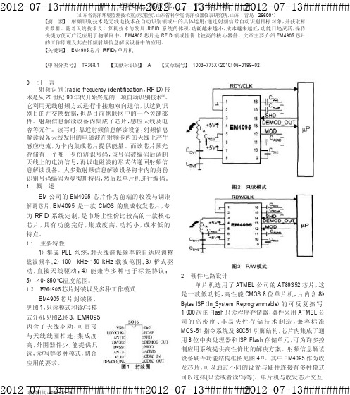
图2 只读模式图3 R/W 模式图1 封装图2012-07-13############李#春##立#,2郭0颜12萍-,0王7-平13,#李#小#峰####2#012-07-13########(山东省海洋环境监测技术重点实验实,山东省科学院 海洋仪器仪表研究所,山东 青岛 266001)【摘 要】 射频识别技术是无线电技术在自动识别领域中的具体运用;通过射频信号自动识别目标对象,并获取相关数据。
随着天线技术及计算机技术的发展,R FID 系统的体积、功耗越来越小,成本越来越低,功能日趋灵活,操作 快捷方便可广泛应用于物联网中。
EM4905 芯片是 RFID 领域性价比较高的核心器件。
文章主要介绍 EM4905 芯片 的工作原理及其在低频射频信息解读设备中的应用。
【关键词】 EM4905 芯片;RFID ;单片机 【中图分类号】 TP368.1【文献标识码】 A【文章编号】 1003-773X(2010)06-0199-02 0 引 言 射频识别(radio frequency identification ,RFID )技术是从 20 世纪 90 年代开始兴起的一项自动识别技术[1]。
它利用无线射频方式进行非接触双向通信,以达到识 别目的并交换数据,也是目前物联网中的一个关键部 件。
射频信息解读设备内集成了芯片,感应天线及电 容等元件。
读写时,靠近射频信息解读设备,射频信息 解读设备天线发出的电磁波在射频卡内的天线上产生 感应电流,为卡内集成芯片提供能量。
而该芯片预先 存储有一个唯一身份辨识号码,该号码被编码后调制 天线上的电流信号,再以电磁波的形式传递回射频信 息解读设备。
大多数射频信息解读设备将卡内的身份 识别号码编码为曼彻斯特码,然后以单片机进行编码。
1 概 述EM 公司的 EM4095 芯片作为前端的收发与调制 解调芯片,E M4095 是一款 CMOS 的集成收发芯片,专 为 RFID 系统定制,是市场上性价比较高的一款核心 芯片,具有功能完好,集成度高,功耗小,成本低的 特点。
射频卡应用中的曼彻斯特码解码技术

器…。大多数射频卡将卡内的身份辨识号码(ID号码)编码为曼 彻斯特码,然后由单片机进行解码。
然而,目前的很多单片机解码程序采用定时查询或考察 信号的边沿状态的方式解码,这些解码方法对天线上的载波 频率要求比较高,对定时的准确度要求也比较高,当载波稍 微偏离规定的范围内时将不能正确读卡。本文介绍了一种新 的解码技术,载波频率的偏移对解码没有任何影响,而且不 用检测信号的边沿状态,从而更加可靠、快速地读卡。
调制到此载波信号上面,通过信号的耦合,EM4095的天线
上也产生带有64位ID号码的调制信号,然后通过EM4095
的解调系统,滤除载波卜”,将64位数据传送给单片机,由
单片机再解码出其中的ID号码。
射频卡内的EM4100芯片内部有预先存储的不可改写的
64位数据,当其通过天线向外输出时,格式如图2所示f2J。
5结语
经过实际的应用,采用这种解码方法可以在读曼彻斯特 码的同时进行同步解码,速度比较快,而且由于对载波频率 的变化不敏感,故读卡成功率非常高。
曼码
上一帻
图5 曼彻斯特码解码分析图 在同步头形成的连续8个T间隔之后,随后的下降沿间 隔可能是T、1.5T或2T。当这个间隔为T时,电平为“LH”, 其中“L”电平要与同步头中第9个l的“H”电平结合,解 出第9个1,同时余下另一个“H”电平等待与后续电平结合; 同理,如果宽为1.5T时,只能解为“LLH”,这样也可以找 到同步头的第9个l,同时可以解出随后的第一位数据“0”。 当间隔为2T时,电平为“LLHH”,除第一个“L”与前面剩 余的“H”结合外,还可以解出一位数据“0”,同时,余下 一个“H”电平等待与后续电平结合。 依照这样的规则,继续对检测到的每一个下降沿间隔进 行解码。在解码过程中,当遇到T时,上次解码必然剩余一
一种RFID的曼彻斯特解码技术
一种RFID的曼彻斯特解码技术康文广;王辉映【摘要】对射频芯片输出的数据进行解码是射频卡应用系统中的关键问题.通过分析EM4095的工作原理和EM4100的编码机制,得出射频芯片输出64位曼彻斯特码的特点,并给出了软件实现算法.利用中断捕获脉宽的方法进行解码,不但硬件接口简单,而且解码速度快,准确率高,同时也为曼彻斯特解码算法提供了一种新的思路.【期刊名称】《单片机与嵌入式系统应用》【年(卷),期】2010(000)012【总页数】3页(P20-22)【关键词】RFID;曼彻斯特码;解码【作者】康文广;王辉映【作者单位】珠海优特电力科技股份有限公司,珠海,519070;珠海优特电力科技股份有限公司,珠海,519070【正文语种】中文【中图分类】TP311射频识别(Radio Frequency Identification,RFID)应用是目前发展最为迅速、潜力最大的新兴技术之一,其利用射频信号和空间耦合(电磁耦合或电磁传播)传输特性,实现对被识别物体的自动识别。
RFID技术正在逐步应用于物流管理、产品生产线、零售业、安保等诸多领域[1]。
本文以EM 4095和EM 4100芯片为例阐述曼彻斯特解码方法。
1 RFID读卡系统的构成如图1所示,系统由读卡器和非接触式智能卡(下文简称RFID卡)组成。
读卡器主要由微控制器、芯片EM 4095和天线组成;智能卡由芯片EM 4100和天线组成。
图1 RFID读卡系统的构成读卡器不断向周围发射固定频率为125 kHz的电磁波,RFID卡内有一个LC串联谐振电路,其工作频率与EM 4095相对应,也为125 kH z,这样当RFID卡进入该磁场空间时,在电磁激励下LC谐振电路产生共振。
通过共振为RFID卡(EM 4100)提供了能量,于是RFID卡通过电磁耦合将自身的ID信息调制后按顺序发送到EM 4095,芯片EM 4095获得此信息后通过解调从引脚DEMOD_OUT输出曼彻斯特码到微控制器。
- 1、下载文档前请自行甄别文档内容的完整性,平台不提供额外的编辑、内容补充、找答案等附加服务。
- 2、"仅部分预览"的文档,不可在线预览部分如存在完整性等问题,可反馈申请退款(可完整预览的文档不适用该条件!)。
- 3、如文档侵犯您的权益,请联系客服反馈,我们会尽快为您处理(人工客服工作时间:9:00-18:30)。
4 5 6 7 8
EM4095
13 12 11 10 9
µP
UPLINK
Signal on Transceiver coil Signal on Transponder coil
DOWNLINK
Signal on Transceiver coil Signal on Transponder coil
RDY/CLK
1 2 3 16 15 14
-
Data transmission by Amplitude Modulation with externally adjustable modulation index using single ended driver Multiple transponder protocol compatibility (Ex: EM400X, EM4050, EM4150, EM4070, EM4170, EM4069….) Sleep mode 1µA USB compatible power supply range 40 to +85°C temperature range Small outline plastic package SO16 Applications Car immobiliser Hand held reader Low cost reader
EM4095 P4095
13 12 11 10 9
µP
DVDD DVSS ANT2 VDD DEMOD_IN
Fig. 1
Fig. 3
Read/Write Mode
RDY/CLK
1 2 3 16 15 14
CDC2 CFCAP SHD DEMOD_OUT MOD CAGND CDEC
LA CRES CDV1 CDV2
元器件交易网
EM MICROELECTRONIC - MARIN SA
EM4095
Read/Write analog front end for 125kHz RFID Basestation
Description The EM4095 (previously named P4095) chip is a CMOS integrated transceiver circuit intended for use in an RFID basestation to perform the following functions: antenna driving with carrier frequency AM modulation of the field for writable transponder AM demodulation of the antenna signal modulation induced by the transponder communicate with a microprocessor via simple interface. Features Integrated PLL system to achieve self adaptive carrier frequency to antenna resonant frequency No external quartz required 100 to 150 kHz carrier frequency range Direct antenna driving using bridge drivers Data transmission by OOK (100% Amplitude Modulation) using bridge driver Typical Operating Configuration Read Only Mode
+5V
4 5 6 7 8
EM4095 P4095
13 12 11 10 9
µP
+5V
Fig. 2
Copyright 2002, EM Microelectronic-Marin SA
1
元器件交易网
EM4095
System principle
Pin Assignment
SO16
CDC2 CFCAP SHD DEMOD_OUT MOD CAGND CDEC VSS RDY/CLK ANT1 DC2 FCAP SHD DEMOD_OUT MOD AGND CDEC_IN CDEC_OUT
+5V LA CRES CDV1 CDV2 +5V
4 5 6 7 8
Copyright 2002, EM Microelectronic-Marin SA
3
元器件交易网
Байду номын сангаас
EM4095
Electrical and Switching Characteristics: Parameters specified below are valid only in case the device is used according to Operating Conditions defined on previous page. VSS=DVSS=0V, VDD =DVDD = 5V, Tj = -40 to 110°C, unless otherwise specified Parameter Symbol Test Conditions Min Typ Max Units Supply current in sleep mode IDDsleep 1 2 µA Supply current excluding drivers IDDon 5 7 mA current VAGND AGND level Note 1 2.35 2.5 2.65 V Logic signals SHD, MOD, DEMOD_OUT Input logic high Input logic low Output logic high Output logic low MOD pull down resistor SHD pull up resistor PLL Antenna capture frequency range Antenna locking frequency range Drivers ANT drivers output resistance RDY/CLK driver output resistance AM demodulation DEMOD_IN common mode range VCM VSS + 0.5 VDD - 0.5 V DEMOD_IN input sensitivity Vsense Note 2 0.85 2 mVpp Note 1: AGND is a EM4095 internal reference point. Any external connection except specified capacitor to VSS may lead to device malfunction. Note 2: Modulating signal 2Khz square wave on 125 kHz carrier, total signal inside VCM
* ±10% tolerance capacitors should be used ** According to 1S2P JEDEC test board Due to antenna driver current the internal junction temperature is higher than ambient temperature. Please calculate ambient temperature range from max. antenna current and package Thermal Resistor. It is the user's responsibility to guarantee that TJ remains below 110°C. Supply voltage (VDD and DVDD pads) must be blocked by a 100nF capacitor (to VSS) as close as possible to the chip
Transponder
Transceiver R/W configuration
RDY/CLK
1 2 3 16 15 14
Coil1 Read Only and R/W Chip Coil2
CDC2 CFCAP SHD DEMOD_OUT MOD CAGND CDEC
+5V LA CRES CDV1 CDV2 +5V
RF Carrier
Data
RF Carrier
Data
Fig. 4
Copyright 2002, EM Microelectronic-Marin SA
2
元器件交易网
EM4095
Absolute Maximum Ratings Parameter Storage temperature Maximum voltage at VDD Minimum voltage at VDD Max. voltage other pads Min. voltage other pads Max. junction temperature Electrostatic discharge max. to MIL-STD-883C method 3015 against VSS Electrostatic discharge max. to MIL-STD-883C method 3015 (only for pins ANT1 and ANT2) against VSS Maximum Input/Output current on all pads except VDD, VSS, DVDD, DVSS, ANT1, ANT2, RDY/CLK Maximum AC peak current on ANT1 and ANT2 pads 100 kHz duty cycle 50% Symbol Conditions TSTO -55 to +150°C VDDmax VSS+6V VDDmin VSS -0.3V VMAX VDD +0.3V VMIN VSS -0.3V TJMAX +125°C VESD VESD_ANT 4000V 10000V Handling Procedures This device has built-in protection against high static voltages or electric fields; however, anti-static precautions must be taken as for any other CMOS component. Unless otherwise specified, proper operation can only occur when all terminal voltages are kept within the voltage range. Unused inputs must always be tied to a defined logic voltage level. Operating Conditions Parameter Operating junction temperature Supply voltage Antenna circuit resonant frequency AC peak current on ANT1 & ANT2 pads CFCAP CDEC CDC2 CAGND Package thermal resistor SO16 Symb TJ VDD FRES IANT * * * 100 69 10 100 6.80 70 Min -40 4.1 100 Typ Max +110 5.5 150 250 * * * 220 71 Units °C V kHz mA nF nF nF nF °C/W
