HCF4051B_02中文资料
HCF4053
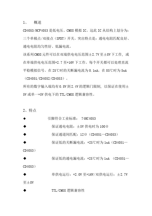
1、概述CD4053/HCF4053是低电压、CMOS模拟IC。
这此IC从结构上划分为:三个单极点/双接点(SPDT)开关。
突出特点是:通电电阻匹配良好、通电电阻均匀性好、低漏电流。
该系列CMOS元件可以在双端供电电压范围±2.7V至±8V下工作, 或在单端供电电压范围+2.7至+16V下工作。
每个开关都可以处理直流平稳模拟信号。
在25℃时的关断漏电流为0.1nA,在85℃时为5nA (CD4051/CD4052/CD4053)。
所有的数字输入端均有0.8V到2.4V的逻辑门限制, 以保证在使用±5V或单一+5V供电下的TTL/CMOS逻辑兼容性。
2、特点◆引脚符合工业标准: 74HC4053◆保证通电电阻:±5V供电时为100Ω◆保证通道间匹配:12Ω(CD4051—CD4053)◆保证低的关断漏电流:+25℃时为1nA(CD4051—CD4053)◆保证低的通电漏电流:+25℃时为1nA (CD4051—CD4053)◆单供电运行:+2.0V至+16V/双供电运行:±2.7V 至±8V◆TTL/CMOS逻辑兼容性◆低损耗:<0.04%(600Ω)◆低色度亮度干扰:<-90dB(50Ω)◆高关断绝缘:<-90dB(50Ω)序号符号功能序号符号功能11Y1Y输入9C控制脚20Y0Y输入10B控制脚31Z1Z输入11A控制脚4Z-common Z公共输出120X0X输入50Z0Z输入131X1X输入6INH 禁止端子,高电位时各开关均切断14x-common X公共输出7VEE负电源15y-common Y公共输出8VSS地16VDD电源。
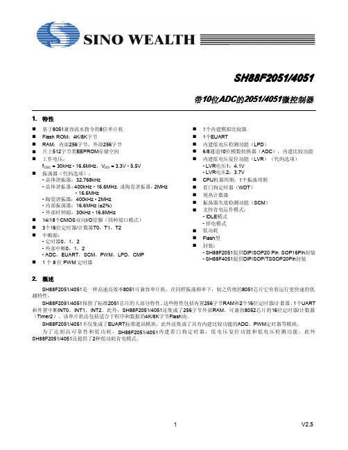
中颖单片机2051_4051资料
P4.0 - P4.2
Internal 256 Bytes External 256 Bytes Data RAM
I/Os Port 1 Configuration I/Os
P3.0 - P3.5 P3.7
P1.0 - P1.7
Timer 0 (16bit) Timer 1 (16bit) Timer 2 (16bit)
电源和时钟控制寄存器: PCON,SUSLO LPD寄存器: LPDCON Flash寄存器: IB_OFFSET,XPAGE,IB_DATA ,IB_CON1,IB_CON2 ,IB_CON3 ,IB_CON4 ,IB_CON5, FLASHCON 数据存储页寄存器: XPAGE 系统时钟控制寄存器: CLKCON 硬件看门狗定时器寄存器:RSTSTAT 中断系统寄存器 IEN0,IEN1,IPH0,IPL0,IPH1,IPL1,EXF0 I/O 端口寄存器: P1,P3,P4,P1M0,P1M1,P3M0,P3M1,P4M0,P4M1 定时器寄存器: TCON,TMOD,TL0,TH0,TL1,TH1,TCON1,T2CON,T2MOD,RCAP2H,RCAP2L EUART寄存器: SCON,SBUF,SADEN,SADDR,PCON ADC寄存器: ADCON,ADT,ADCH,ADDL,ADDH CMP寄存器: CMPCON PWM寄存器: PWMCON,PWMP,PWMD
1
V2.5
SH88F2051 /4051 SH88F2051/
3. 方框图
VDD Reset circuit Power Pipelined 8051 architecture RESET
Watch Dog
4K/8 K Bytes Flash ROM
CD4051 CD4052 CD4053中文资料PDF 引脚功能

CD4051 CD4052 CD4053中文资料PDF 引脚功能CD4051/CC4051是单8通道数字控制模拟电子开关,有三个二进控制输入端A、B、C和I NH输入,具有低导通阻抗和很低的截止漏电流。
幅值为4.5~20V的数字信号可控制峰值至2 0V的模拟信号。
例如,若VDD=+5V,VSS=0,VEE=-13.5V,则0~5V的数字信号可控制-13.5~4.5V的模拟信号。
这些开关电路在整个VDD-VSS和VDD-VEE电源范围内具有极低的静态功耗,与控制信号的逻辑状态无关。
当INH输入端=“1”时,所有的通道截止。
三位二进制信号选通8通道中的一通道,可连接该输入端至输出。
CD4052/CC4052是一个差分4通道数字控制模拟开关,有A、B两个二进制控制输入端和INH输入,具有低导通阻抗和很低的截止漏电流。
幅值为4.5~20V的数字信号可控制峰峰值至20V的模拟信号。
例如,若V DD=+5V,VSS=0,VEE=-13.5V,则0~5V的数字信号可控制-13.5~4.5V的模拟信号,这些开关电路在整个VDD-VSS和VDD-VEE电源范围内具有极低的静态功耗,与控制信号的逻辑状态无关,当INH输入端=“1”时,所有通道截止。
二位二进制输入信号选通4对通道中的一通道,可连接该输入至输出。
CD4053/CC4053是三2通道数字控制模拟开关,有三个独立的数字控制输入端A、B、C和INH输入,具有低导通阻抗和低的截止漏电流。
幅值为4.5~20V的数字信号可控制峰-峰值至20V的数字信号。
例如若VDD=+5,VSS=0,VEE=-13.5V,则0~5V的数字信号可控制-13.5~4.5V的模拟信号。
这些开关电路在整个VDD-VSS和VDD-VEE电源范围内具有极低的静态功耗,与控制信号的逻辑状态无关。
当INH输入端=“1”时,所有通道截止。
控制输入为高电平时,“0”通道被选,反之,“1”通道被选。
CD4051引脚图CD4052引脚图CD4053引脚图CD4051逻辑图CD4052逻辑图CD4053逻辑图切换时间波形图Absolute Maximum Ratings 绝对最大额定值:Recommended Operating Conditions 建议操作条件:DC Electrical Characteristics 直流电气特性:DC Electrical Characteristics 直流电气特性:AC Electrical Characteristics 交流电气特性:相关下载:cd4051中文资料,。
4051中文资料
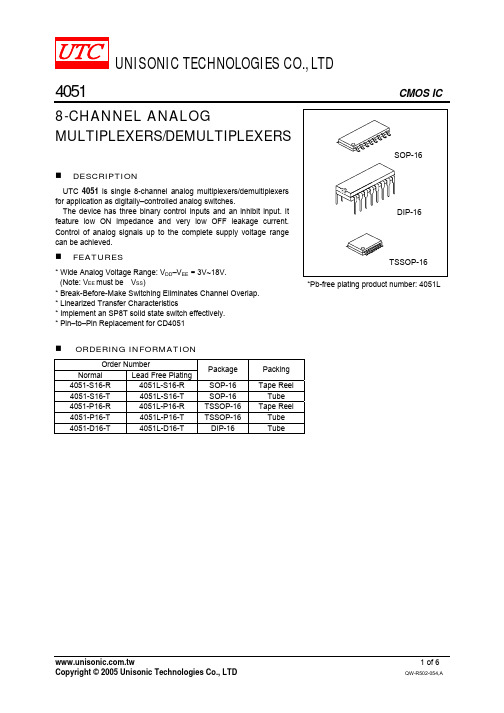
4051CMOS ICMULTIPLEXERS/DEMULTIPLEXERSDESCRIPTIONUTC 4051 is single 8-channel analog multiplexers/demultiplexersfor application as digitally–controlled analog switches.The device has three binary control inputs and an inhibit input. Itfeature low ON impedance and very low OFF leakage current.Control of analog signals up to the complete supply voltage rangecan be achieved.FEATURES* Wide Analog Voltage Range: V DD–V EE = 3V~18V.(Note: V EE must be V SS)*Pb-free plating product number: 4051L * Break-Before-Make Switching Eliminates Channel Overlap.* Linearized Transfer Characteristics* Implement an SP8T solid state switch effectively.* Pin–to–Pin Replacement for CD4051ORDERING INFORMATIONOrder NumberPackage PackingNormal Lead Free PlatingReel4051-S16-R 4051L-S16-R SOP-16 Tape4051-S16-T 4051L-S16-T SOP-16 TubeTSSOP-16TapeReel4051-P16-R 4051L-P16-RTSSOP-16Tube4051-P16-T 4051L-P16-T4051-D16-T 4051L-D16-T DIP-16 TubePIN CONFIGURATION1 2 3 4 5 6 7 8161514131211109X1V DDX2ABC UTC 4051X4 X6 XX7 X5 INH V EE V SS X0 X3PIN DESCRIPTIONPIN No. SYMBAL NAME AND FUNCTION3 XCommonInput/Output6 INHInhibitInputs7 V EE SupplyVoltage8 V SS Ground11,10,9 A,B,CBinary Control Inputs13,14,15,12,1,5,2,4 X0~X7 IndependentInputs/Outputs16 V DD Positive Supply VoltageABSOLUTE MAXIMUM RATINGPARAMETER SYMBOL RATINGS UNITDC Supply Voltage (Referenced to V EE , V SS V EE ) V DD -0.5 ~ +18 V Input or Output Voltage (DC or Transient)(Referenced to V SS for Control Inputs and V EE for Switch I/O) V IN , V OUT -0.5 ~ V DD +0.5 VInput Current (DC or Transient), per Control Pin I IN ±10 mA Switch Through Current I SW ±25 mAPower Dissipation Derating above 65℃ P D 500 7mW mW/℃ Junction Temperature T J 125 ℃ Operating Temperature Range T OPR -40 ~ +125℃ Storage Temperature Range T STG -40 ~ +150℃ Note: 1.Absolute maximum ratings are those values beyond which the device could be permanently damaged.Absolute maximum ratings are stress ratings only and functional device operation is not implied.2.The device is guaranteed to meet performance specification within 0 ~70 operating temperature range and assured by design from –40 ~125 . ELECTRICAL CHARACTERISTICS (Ta=25 , unless otherwise specified.)PARAMETER SYMBOL TEST CONDITIONS MIN TYP MAX UNITSUPPLY REQUIREMENTS (Voltages Referenced to V EE )Power Supply Voltage Range V DD V DD – 3.0 V SS V EE3 18 V V DD =5V 0.005 5 V DD =10V 0.010 10Quiescent Current perPackageV DD =15V I Q Control Inputs: V IN = V SS or V DDSwitch I/O: V EE V I/O V DD , and ∆Vsw 500mV(Note 2) 0.015 20 µA V DD =5V (0.07 µA/kHz) f + I Q V DD =10V (0.20 µA/kHz) f + I Q Total Supply Current(Dynamic Plus Quiescent, Per Package) V DD =15VI D(AV) T a =25 only (The channel component, (V IN -Vout)/Ron, is not included.) (0.36 µA/kHz) f + I Q µASWITCHES IN/OUT AND COMMONS OUT/IN -- X, Y, Z (Voltages Referenced to V EE ) Recommended Peak–to–PeakVoltage Into or Out of the Switch V I/O Channel On or Off 0 V DD V PPRecommended Static or DynamicVoltage Across the Switch ∆Vsw Channel On 0 600 mVOutput Offset Voltage V O(OFF)V IN = 0V, No Load 10 µVV DD =5V 250 1050V DD =10V 120 500ON Resistance V DD =15V R ON ∆Vsw 500mV V IN = V IL or V IH (Control), and V IN = 0 to V DD (Switch) 80 280Ω V DD =5V 25 70V DD =10V 10 50ON Resistance Between Any Two Channels in the Same Package V DD =15V∆R ON 10 45 Ω Off–Channel Leakage Current I OFF V IN = V IL or V IH (Control)Channel to Channel or AnyOne Channel, V DD =15V±0.05 ±100 nA Capacitance, Switch I/O C I/O Inhibit = V DD 10 pF Capacitance, Common O/I C O/I Inhibit = V DD 17 pFCapacitance, Feedthrough(Channel Off)C I/OPins Not Adjacent Pins Adjacent 0.15 0.47 pFELECTRICAL CHARACTERISTICS(Cont.)PARAMETER SYMBOL TEST CONDITIONS MIN TYP MAX UNITCONTROL INPUTS – INHIBIT A, B, C (Voltages Referenced to V SS )V DD =5V 2.25 1.5V DD =10V 4.50 3.0Low Level Input Voltage V DD =15V V IL R ON = per spec, I OFF = per spec 6.75 4.0 V V DD =5V 3.5 2.75V DD =10V 7 5.5High Level Input Voltage V DD =15V V IH R ON = per spec, I OFF = per spec 11 8.25V Input Leakage Current I LEAK V IN = 0 or V DD , V DD =15V ±0.00001 ±0.1µA Input Capacitance C IN 5.0 7.5 pFDYNAMIC ELECTRICAL CHARACTERISTICS(C L = 50pF, T a =25 , V EE V SS , unless otherwise specified)PARAMETER SYMBOLV DD –V EEVdcTEST CONDITIONS MIN TYP MAX UNIT Propagation Delay Times Switch Input to Switch Output (R L = 10 k Ω) t PLH, t PHL510 15 t PLH , t PHL =(0.17 ns/pF)C L + 26.5ns t PLH , t PHL =(0.08 ns/pF)C L + 11ns t PLH , t PHL =(0.06 ns/pF)C L + 9ns35 15 12 90 40 30 ns Inhibit to Outputt PHZ, t PLZt PZH, t PZL510 15 (R L =10k Ω, V EE =V SS ) Output “1” or “0” to High Impedance, or High Impedance to “1” or “0” Level350 170 140 700340280ns Control Input to Output t PLH, t PHL 510 15 R L = 10 k Ω, V EE = V SS360 160 120 720320240ns Total Harmonic Distortion THD 10 R L = 10K Ω, f = 1 kHz, Vin = 5 V PP 0.07 %Bandwidth BW 10 R L = 1k Ω, V IN = 1/2 (V DD –V EE ) p–p, C L = 50pF, 20 Log (Vout/Vin) = -3dB)17 MHzOff Channel Feedthrough Attenuation 10 R L =1K Ω, V IN = 1/2 (V DD –V EE ) p–p f IN = 4.5 MHz-50 dBChannel Separation 10 R L = 1k Ω, V IN = 1/2 (V DD –V EE ) p–p f IN = 3MHz-50 dBCrosstalk, Control Input to Common O/I 10 R 1 = 1k Ω, R L = 10k Ω Control t TLH = t THL = 20ns, Inhibit = V SS75 mVNote 1. Data of “TYP” is intended as an indication of the IC’s potential performance.2. For voltage drops across the switch(∆Vsw)>600mV (>300mV at high temperature), excessive V DD current may be drawn, i.e. the current out of the switch may contain both V DD and switch input components. The reliability of the device will be unaffected unless the Maximum Ratings are exceeded.TEST CIRCUITSwitch Circuit SchematicTRUTH TABLEControl InputsINHIBIT C B AON Switches0 0 0 0 0 0 0 0 0 1 0 1 0 0 1 1 X0 X1 X2 X3 0 0 0 01 0 0 1 0 1 1 1 0 1 1 1X4 X5 X6 X7 1 x x x Nonex = Don’t Care9B 1C A 6INH X4 1X5 5X6 2X7 43XUTC 4051Functional DiagramTYPICAL CHARACTERISTICSInput Voltage, V IN (V)Input Voltage , V IN (V )"O N " R e s i s ta n c e , R O N300350200Input Voltage , V IN (V)"O N " R e s i s t a n c e , R O N( )25015010050。
4051芯片手册
4051芯片手册
4051芯片是一种多路复用器/解复用器,通常用于模拟信号和数字信号的互连。
以下是4051芯片的一些常见应用和功能:
1.多路复用/解复用:4051芯片可以将多个输入通道合并到一个输出通道,或
者将一个输入通道分配到多个输出通道。
这使得它在模拟信号处理和开关
应用中非常有用。
2.数字控制:4051芯片可以通过数字控制信号来选择输入/输出通道之间的连
接。
这使得它可以实现数字开关、数字选择器和解码器等功能。
3.缓冲和驱动:4051芯片可以作为输入和输出缓冲器,用于驱动或吸收电
流,并可提供额外的电压或电流增益。
4.电压或电流检测:4051芯片可以用于检测电压或电流信号,并将其转换为
数字信号,以便于处理和控制。
需要注意的是,具体的4051芯片手册可能会有所不同,具体内容应根据芯片的型号和制造商来确定。
TC4051BP_07中文资料
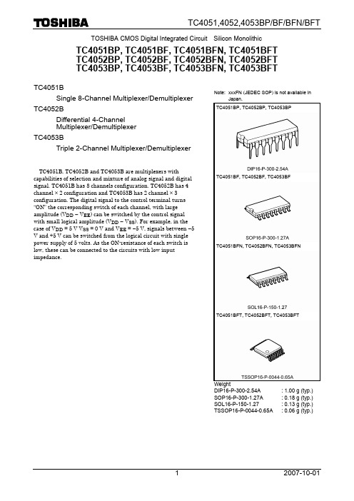
4
2007-10-01
元器件交易网 Operating Ranges (Note)
TC4051,4052,4053BP/BF/BFN/BFT
Characteristics
Symbol
Test Condition
Min Typ. Max Unit
DC supply voltage
0.5 to 5 × 10² Ω
>109 Ω
(Note)
Note: See electrical characteristics
OUT c IN
TC4051,4052,4053BP/BF/BFN/BFT
7 VEE
OUT c IN OUT c IN OUT c IN OUT c IN OUT c IN OUT c IN
VDD-VSS
−0.5 to 20
V
VDD-VEE
−0.5 to 20
V
VCIN
VSS − 0.5 to VDD + 0.5
V
VI/VO
VEE − 0.5 to VDD + 0.5
V
ICIN
±10
mA
Potential difference across I/O during ON
VI-VO
−0.5 to 0.5
Static Electrical Characteristics
Characteristics
Control input high voltage
Control input low voltage
On-state resistance
ΔOn-state resistance between any 2 switches Input/output leakage current
TC74VHC4051AFT中文资料

TOSHIBA CMOS Digital Integrated Circuit Silicon MonolithicTC74VHC4051AF,TC74VHC4051AFT,TC74VHC4051AFKTC74VHC4052AF,TC74VHC4052AFT,TC74VHC4052AFKTC74VHC4053AF,TC74VHC4053AFT,TC74VHC4053AFK TC74VHC4051AF/AFT/AFK8-Channel Analog Multiplexer/DemultiplexerTC74VHC4052AF/AFT/AFKDual 4-Channel Analog Multiplexer/DemultiplexerTC74V4053AF/AFT/AFKTriple 2-Channel Analog Multiplexer/DemultiplexerThe TC74VHC4051A/4052A/4053A are high-speed, low-voltage drive analog multiplexer/demultiplexers using silicon gate CMOS technology. In 3 V and 5 V systems these can achieve high-speed operation with the low power dissipation that is a feature of CMOS.The TC74VHC4051A/4052A/4053A offer analog/digital signal selection as well as mixed signals. The 4051A has an 8-channel configuration, the 4052A has an 4-channel × 2 configuration, and the 4053A has a 2-channel × 3 configuration.The switches for each channel are turned ON by the control pin digital signals.All control inputs are equipped with a newly developed input protection circuit that avoids the need for a diode on the plus side (forward side from the input to the V CC). As a result, for example, 5.5 V signals can be permitted on the inputs even when the power supply voltage to the circuits is off. As a result of this input power protection, the TC74VHC4051A/4052A/4053A can be used in a variety of applications, including in the system which has two power supplies, and in battery backup circuits.Features•Low ON resistance: R on = 45Ω (typ.) (V CC = 3 V)R on = 24Ω (typ.) (V CC = 4.5 V)•Low power dissipation: I CC= 2.0 μA (max) (Ta = 25°C) •Input level: V IL= 0.8V (max) (V CC = 3 V) V IH= 2.0V (min) (V CC = 3 V)•Power down protection is provided on all control inputs TC74VHC4051AF, TC74VHC4052AF,TC74VHC4053AFTC74VHC4051AFT, TC74VHC4052AFT,TC74VHC4053AFTTC74VHC4051AFK, TC74VHC4052AFK,TC74VHC4053AFKSOP16-P-300-1.27A : 0.18 g ( typ.) TSSOP16-P-0044-0.65A : 0.06 g ( typ.) VSSOP16-P-0030-0.50 : 0.02 g ( typ.)Pin Assignment (top view)Truth TableControl Inputs“ON” ChannelInhibit C *BA VHC4051A VHC4052A VHC4053AL L L L 0 0X, 0Y 0X, 0Y, 0Z L L L H 1 1X, 1Y 1X, 0Y,0Z L L H L 2 2X, 2Y 0X, 1Y, 0Z LLHH33X, 3Y1X, 1Y, 0ZL H L L 4 ⎯ 0X, 0Y, 1Z L H L H 5 ⎯ 1X, 0Y, 1Z L H H L 6 ⎯ 0X, 1Y,1Z L H H H7⎯ 1X, 1Y, 1ZH X X X None None NoneX: Don't care, *: Except VHC4052AFT1 14 0 3 A B C13 12 11 10 915 4 6 COM 7 5 INH GND 2 816 GND V CC 1X 14 X-COM 0X 3X A B13 12 11 10 915 0Y 12345672Y Y-COM 3Y 1Y INH GND 816 GND V CC X-COM 14 1X 0X A B C13 12 11 10 915 1Y 0Y 1Z Z-COM 0Z INH GND Y-COM 816 GND V CCSystem DiagramTC74VHC4051ATC74VHC4052ATC74VHC4053ACOM 01 2 3 45 67X-COM0X 1X 2X 3X 0Y 1Y 2Y3Y Y-COMX-COM0X 1X0Y 1Y0Z 1Z Z-COMY-COMAbsolute Maximum Ratings (Note)Characteristics Symbol Rating Unit Power supply voltage V CC−0.5~7.0 VControl input voltage V IN−0.5~7.0 VSwitch I/O voltage V I/O − 0.5~V CC+ 0.5VInput diode current I IK−20 mAI/O diode current I IOK±25 mASwitch through current I T±25 mADC V CC or ground current I CC±50 mAmW Power dissipation P D 180Storage temperature T stg−65~150 °CNote : Exceeding any of the absolute maximum ratings, even briefly, may lead to deterioration in IC performance or even destruction.Using continuously under heavy loads (e.g. the application of high temperature/current/voltage and thesignificant change in temperature, etc.) may cause this product to decrease in the reliability significantlyeven if the operating conditions (i.e. operating temperature/current/voltage, etc.) are within the absolutemaximum ratings and the operating ranges.Please design the appropriate reliability upon reviewing the Toshiba Semiconductor Reliability Handbook(“Handling Precautions”/“Derating Concept and Methods”) and individual reliability data (i.e. reliability testreport and estimated failure rate, etc).Operating Range (Note)Characteristics Symbol Rating Unit Power supply voltage V CC2~5.5 VInput voltage V IN 0~5.5 VSwitch I/O voltage V I/O 0~V CC VOperating temperature T opr−40~85 °C0~200 (V CC= 2.5 ± 0.2 V)ns/VInput rise and fall time dt/dv0~100 (V CC= 3.3 ± 0.3 V)0~20 (V CC= 5 ± 0.5 V)Note: The operating ranges must be maintained to ensure the normal operation of the device.Unused control inputs must be tied to either V CC or GND.Electrical Characteristics DC Electrical CharacteristicsTa = 25°C Ta = −40~85°CCharacteristics Symbol Test ConditionV CC (V)MinTyp.Max Min Max Unit2.0 1.5 ⎯⎯ 1.5 ⎯ 3.0 2.0 ⎯ ⎯2.0⎯ 4.5 3.15 ⎯ ⎯ 3.15 ⎯ High-level V IH⎯5.5 3.85⎯ ⎯ 3.85 ⎯ 2.0⎯ ⎯ 0.5 ⎯ 0.5 3.0 ⎯ ⎯0.8⎯0.8 4.5 ⎯ ⎯ 1.35 ⎯ 1.35Input voltageLow-level V IL⎯5.5⎯ ⎯ 1.65 ⎯ 1.65V2.3 ⎯ 200⎯⎯⎯ 3.0 ⎯ 45 86 ⎯ 108V IN = V IL or V IH V I/O = V CC to GNDI I/O = 2 mA 4.5 ⎯ 24 37 ⎯ 46 2.3 ⎯ 28 73 ⎯ 84 3.0 ⎯ 22 38 ⎯ 44 ON resistanceR ONV IN = V IL or V IH V I/O = V CC or GND I I/O = 2 mA4.5 ⎯ 17 27 ⎯ 31 Ω 2.3 ⎯ 10 25 ⎯ 35 3.0 ⎯ 5 15 ⎯ 20 Difference of ON resistance between switchesΔR ON V IN = V IL or V IHV I/O = V CC to GNDI I/O = 2 mA 4.5⎯5 13 ⎯18Ω Input/Output leakagecurrent(switch OFF)I OFFV OS = V CC or GNDV IS = GND to V CC V IN = V IL or V IH5.5⎯⎯±0.1 ⎯ ±1.0μAInput/Output leakage current(switch ON, output open) I I/O V OS = V CC or GND V IN = V IL or V IH 5.5 ⎯ ⎯ ±0.1 ⎯ ±1.0μA Control input current I IN V IN = V CC or GND 5.5 ⎯ ⎯±0.1 ⎯ ±1.0μA Quiescent supply currentI CCV IN = V CC or GND5.5⎯⎯2.0⎯20.0μAAC Electrical Characteristics (Input: t r = t f = 3 ns)Ta = 25°C Ta = −40~85°CCharacteristics SymbolTest ConditionV CC (V)Min Typ.Max Min MaxUnit2.5±0.2⎯ 1.2 10 ⎯ 16 3.3±0.3⎯ 0.8 6 ⎯ 10 C L = 15 pFR L = 1 k Ω5.0±0.5⎯ 0.3 4 ⎯ 7ns2.5±0.2⎯ 2.6 12 ⎯ 183.3±0.3⎯ 1.5 9 ⎯ 12 Phase difference between input and outputφI/OC L = 50 pF R L = 1 k Ω5.0±0.5⎯ 0.6 6 ⎯ 8 2.5±0.2⎯ 3.3 15 ⎯ 20 3.3±0.3⎯ 2.3 11 ⎯ 15 C L = 15 pF R L = 1 k ΩFigure 15.0±0.5⎯ 1.6 7 ⎯ 10ns 2.5±0.2⎯ 4.2 25 ⎯ 32 3.3±0.3⎯ 3.0 18 ⎯ 22 Output enable timet pZL t pZHC L = 50 pF R L = 1 k ΩFigure 15.0±0.5⎯ 2.1 12 ⎯ 16 2.5±0.2⎯ 6 15 ⎯ 23 3.3±0.3⎯ 4.5 11 ⎯ 15 C L = 15 pF R L = 1 k ΩFigure 15.0±0.5⎯ 3.2 7 ⎯ 10ns 2.5±0.2⎯ 9.6 25 ⎯ 32 3.3±0.3⎯ 7.2 18 ⎯ 22 Output disable timet pLZ t pHZC L = 50 pF R L = 1 k ΩFigure 15.0±0.5⎯ 5.1 12 ⎯ 16 Control input capacitance C IN All types⎯⎯3⎯⎯10 pF4051A 23.44052A 13.1COMMON terminal capacitanceC IS4053A Figure 2⎯ ⎯ 8.2⎯ ⎯ ⎯ pF4051A 5.74052A 5.6SWITCH terminalcapacitanceC OS4053A Figure 2⎯ ⎯ 5.6 ⎯ ⎯ ⎯ pF 4051A 0.54052A 0.5Feedthrough capacitanceC IOS4053A Figure 2⎯ ⎯ 0.5 ⎯ ⎯ ⎯ pF 4051A 154052A 24Power dissipationcapacitanceC PD4053A Figure 2(Note)⎯ ⎯ 12⎯ ⎯ ⎯ pF Note: C PD is defined as the value of the internal equivalent capacitance of IC which is calculated from theoperating current consumption without load.Average operating current can be obtained by the equation: I CC (opr) = C PD ・V CC ・f IN + I CCAnalog Switch Characteristics (Ta = 25°C ) (Note)Characteristics Test ConditionV CC (V)Typ. UnitV IN = 2.0 V p-p 3.0 0.1Sine Wave Distortion (T.H.D)R L = 10 kΩ, C L = 50 pF, f IN = 1 kHzV IN = 4.0 V p-p 4.5 0.03%4051A 150 4052A 200 4053A3.0 2404051A 180 4052A 230 Frequency response(switch ON)V IN is centered at (V CC /2). Adjust input for 0dBm.Increase f IN frequency until dB meter reads −3dB.R L = 50 Ω, C L = 10 pF,sine wave Figure 34053A4.5 280 MHz3.0 -45V IN is centered at (V CC /2). Adjust input for 0dBm.R L = 600 Ω, C L = 50 pF, f IN = 1 MHz, sine wave Figure 44.5 -45 3.0 -65 Feed through attenuation(switch OFF)R L = 50 Ω, C L = 10 pF, f IN = 1 MHz, sine wave 4.5 -65dB 3.0 60Crosstalk(control input to signal output)R L = 600 Ω, C L = 50 pF, f IN = 1 MHz, square wave (t r = t f = 6 ns) Figure 54.5 100 mV 3.0 -45 Crosstalk(between any switches)VIN is centered at (VCC/2). Adjust input for 0dBm. R L = 600 Ω, C L = 50 pF, f IN = 1 MHz, sine wave Figure 64.5 -45 dBNote: These characteristics are determined by design of devices.AC Test CircuitFigure 2 C IOS , C IS , C OSFigure 1 t pLZ , t pHZ , t pZL , t pZHV CCGND V CV OH V OL V OH V OLV O/I(S 1 = V CC , S 2 =V O/I(S 1= GND, S 2 =S2Figure 3 Frequency Response (switch on)1/2V CCFigure 4 FeedthroughV IN 1/2V CCFigure 5 Cross Talk (control input to output signal)V Figure 6 Cross Talk (between any two switches)V IN1/2V CCPackage DimensionsWeight: 0.18 g (typ.)Weight: 0.06 g (typ.)Weight: 0.02 g (typ.)RESTRICTIONS ON PRODUCT USE20070701-EN •The information contained herein is subject to change without notice.•TOSHIBA is continually working to improve the quality and reliability of its products. Nevertheless, semiconductor devices in general can malfunction or fail due to their inherent electrical sensitivity and vulnerability to physical stress. It is the responsibility of the buyer, when utilizing TOSHIBA products, to comply with the standards of safety in making a safe design for the entire system, and to avoid situations in which a malfunction or failure of such TOSHIBA products could cause loss of human life, bodily injury or damage to property.In developing your designs, please ensure that TOSHIBA products are used within specified operating ranges as set forth in the most recent TOSHIBA products specifications. Also, please keep in mind the precautions and conditions set forth in the “Handling Guide for Semiconductor Devices,” or “TOSHIBA Semiconductor Reliability Handbook” etc.• The TOSHIBA products listed in this document are intended for usage in general electronics applications (computer, personal equipment, office equipment, measuring equipment, industrial robotics, domestic appliances, etc.).These TOSHIBA products are neither intended nor warranted for usage in equipment that requires extraordinarily high quality and/or reliability or a malfunction or failure of which may cause loss of human life or bodily injury (“Unintended Usage”). Unintended Usage include atomic energy control instruments, airplane or spaceship instruments, transportation instruments, traffic signal instruments, combustion control instruments, medical instruments, all types of safety devices, etc.. Unintended Usage of TOSHIBA products listed in his document shall be made at the customer’s own risk.•The products described in this document shall not be used or embedded to any downstream products of which manufacture, use and/or sale are prohibited under any applicable laws and regulations.• Please contact your sales representative for product-by-product details in this document regarding RoHS compatibility. Please use these products in this document in compliance with all applicable laws and regulations that regulate the inclusion or use of controlled substances. Toshiba assumes no liability for damage or losses occurring as a result of noncompliance with applicable laws and regulations.。
hcf4021原理

hcf4021原理
HCF4021B是一个单片集成电路,采用金属氧化物半导体技术制造,封装形式为DIP和SOP。
这个装置包含并行8级或串行输入/输出寄存器,具有共同的时钟串行输出寄存器,并行/串行控制输入,单串行数据输入,以及个人并行"JAM"输入到每个寄存器级。
每个寄存器级是D型,主从触发器中除了一个从8级输出,"Q"输出也可从阶段6,7。
串行输入是同步与时钟,而并行输入是异步的。
关于HCF4021的原理,涉及到具体的电路设计和工作机制,这超出了我的知识范围。
如需了解其工作原理,建议咨询相关领域专家或查阅电子工程方面的文献。
CD4051,CD4052,CD4053中文资料
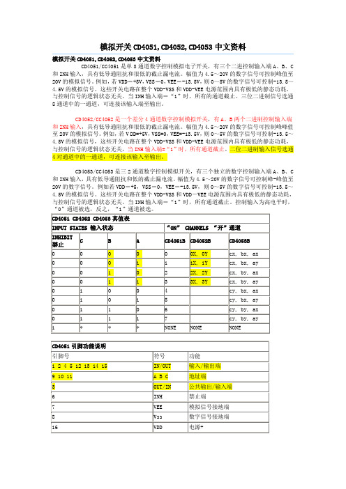
模拟开关CD4051,CD4052,CD4053中文资料模拟开关CD4051,CD4052,CD4053中文资料CD4051/CC4051是单8通道数字控制模拟电子开关,有三个二进控制输入端A、B、C和INH 输入,具有低导通阻抗和很低的截止漏电流。
幅值为4.5~20V的数字信号可控制峰值至20V的模拟信号。
例如,若VDD=+5V,VSS=0,VEE=-13.5V,则0~5V的数字信号可控制-13.5~4.5V 的模拟信号。
这些开关电路在整个VDD-VSS和VDD-VEE电源范围内具有极低的静态功耗,与控制信号的逻辑状态无关。
当INH输入端=“1”时,所有的通道截止。
三位二进制信号选通8通道中的一通道,可连接该输入端至输出。
CD4052/CC4052是一个差分4通道数字控制模拟开关,有A、B两个二进制控制输入端和INH 输入,具有低导通阻抗和很低的截止漏电流。
幅值为4.5~20V的数字信号可控制峰峰值至20V 的模拟信号。
例如,若V DD=+5V,VSS=0,VEE=-13.5V,则0~5V的数字信号可控制-13.5~4.5V 的模拟信号,这些开关电路在整个VDD-VSS和VDD-VEE电源范围内具有极低的静态功耗,与控制信号的逻辑状态无关,当INH输入端=“1”时,所有通道截止。
二位二进制输入信号选通4对通道中的一通道,可连接该输入至输出。
CD4053/CC4053是三2通道数字控制模拟开关,有三个独立的数字控制输入端A、B、C和INH 输入,具有低导通阻抗和低的截止漏电流。
幅值为4.5~20V的数字信号可控制峰-峰值至20V 的数字信号。
例如若VDD=+5,VSS=0,VEE=-13.5V,则0~5V的数字信号可控制-13.5~4.5V 的模拟信号。
这些开关电路在整个VDD-VSS和VDD-VEE电源范围内具有极低的静态功耗,与控制信号的逻辑状态无关。
当INH输入端=“1”时,所有通道截止。
CD4051模拟开关资料
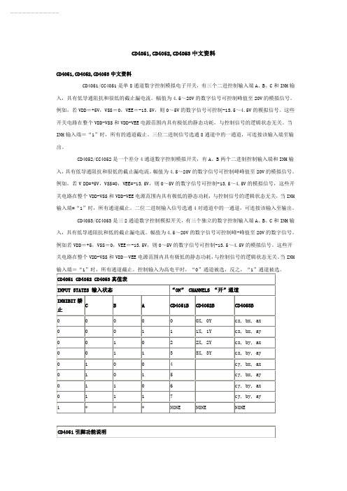
CD4051,CD4052,CD4053中文资料CD4051,CD4052,CD4053中文资料CD4051/CC4051是单8通道数字控制模拟电子开关,有三个二进控制输入端A、B、C和INH输入,具有低导通阻抗和很低的截止漏电流。
幅值为4.5~20V的数字信号可控制峰值至20V的模拟信号。
例如,若VDD=+5V,VSS=0,VEE=-13.5V,则0~5V的数字信号可控制-13.5~4.5V的模拟信号。
这些开关电路在整个VDD-VSS和VDD-VEE电源范围内具有极低的静态功耗,与控制信号的逻辑状态无关。
当INH输入端=“1”时,所有的通道截止。
三位二进制信号选通8通道中的一通道,可连接该输入端至输出。
CD4052/CC4052是一个差分4通道数字控制模拟开关,有A、B两个二进制控制输入端和INH输入,具有低导通阻抗和很低的截止漏电流。
幅值为4.5~20V的数字信号可控制峰峰值至20V的模拟信号。
例如,若V DD=+5V,VSS=0,VEE=-13.5V,则0~5V的数字信号可控制-13.5~4.5V的模拟信号,这些开关电路在整个VDD-VSS和VDD-VEE电源范围内具有极低的静态功耗,与控制信号的逻辑状态无关,当INH 输入端=“1”时,所有通道截止。
二位二进制输入信号选通4对通道中的一通道,可连接该输入至输出。
CD4053/CC4053是三2通道数字控制模拟开关,有三个独立的数字控制输入端A、B、C和INH输入,具有低导通阻抗和低的截止漏电流。
幅值为4.5~20V的数字信号可控制峰-峰值至20V的数字信号。
例如若VDD=+5,VSS=0,VEE=-13.5V,则0~5V的数字信号可控制-13.5~4.5V的模拟信号。
这些开关电路在整个VDD-VSS和VDD-VEE电源范围内具有极低的静态功耗,与控制信号的逻辑状态无关。
当INHCD4051逻辑图CD4051引脚图CD4052逻辑图 CD4052引脚图CD4053逻辑图 CD4053引脚图。
HCF4052中文资料

200
mW
100
mW
– 55 to + 125
°C
– 40 to + 85
°C
Ts tg Storage Temperature
– 65 to + 150
°C
Stresses above those listed under ”Absolute Maximum Ratings” may cause permanent damage to the device. This is a stress rating only and functional operation of the device at these or any other conditions above those indicated in the operational sections of this specification is not implied. Exposure to absolute maximum rating conditions for external periods may affect device r eli abil ity . * All voltage values are referred to VSS pin voltage.
. BINARY ADDRESS DECODING ON CHIP . VERY LOW QUIESCENT POWER DISSIPA-
TION UNDER ALL DIGITAL CONTROL INPUT AND SUPPLY CONDITIONS : 0.2 µW (typ.), VDD – VSS = VDD – VEE = 10V
M74HC4052B1R资料

V
VCC - VEE Supply Voltage Range
-0.5 to 13
V
VIN
Control Input Voltage
-0.5 to VCC + 0.5
V
VI/O
Switch I/O Voltage
ICK
Control Input Diode Current
IIOK
I/O Diode Current
Difference of ON Resistance Between Switches
Test Conditions
VCC VEE (V) (V)
TA = 25 oC 54HC and 74HC
Value
-40 to 85 oC -55 to 125 oC Unit
74HC
54HC
Min. Typ. Max. Min. Max. Min. Max.
VEE - 0.5 to VCC + 0.5
V
± 20
mA
± 20
mA
IT
Switch Through Current
± 25
mA
ICC
DC VCC or Ground Current
± 50
mA
PD
Power Dissipation
Tstg
Storage Temperature
TL
Lead Temperature (10 sec)
5/15
元器件交易网
M54/M74HC4051/4052/4053
RECOMMENDED OPERATING CONDITIONS
Symbol VCC VEE
VCC - VEE VIN VI/O Top
三极管c4051参数

三极管c4051参数
C4051是一种16通道模拟多路复用器/解复用器,它具有以下
主要参数:
1. 通道数,C4051具有16个通道,可以实现16路信号的复用
和解复用功能。
2. 控制电压范围,C4051的控制电压范围通常为0V至VCC,VCC是芯片的供电电压。
3. 输入高电平范围,C4051的输入高电平范围通常为VCC-0.5V,VCC是芯片的供电电压。
4. 输入低电平范围,C4051的输入低电平范围通常为+0.5V。
5. 通道内阻,C4051的通道内阻较小,通常为50欧姆。
6. 供电电压范围,C4051的供电电压范围通常为3V至18V,具
体取决于制造商的规格要求。
7. 工作温度范围,C4051的工作温度范围通常为-55°C至
+125°C,这使得它在各种环境条件下都能正常工作。
以上是C4051三极管的一些主要参数,这些参数可以帮助工程师在设计电路时了解并合理应用这种器件。
希望这些信息能够对你有所帮助。
HCC4052BM1中文资料
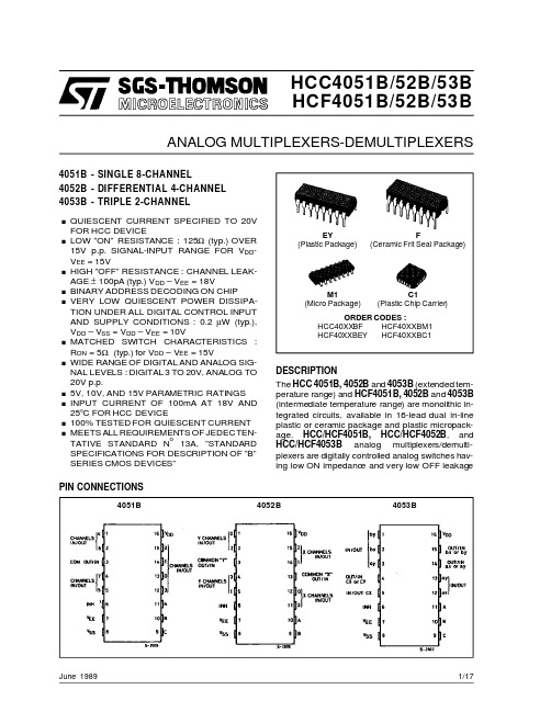
HCC4051B/52B/53B HCF4051B/52B/53BANALOG MULTIPLEXERS-DEMULTIPLEXERS.QUIESCENT CURRENT SPECIFIED TO 20V FOR HCC DEVICE.LOW ”ON”RESISTANCE :125Ω(typ.)OVER 15V p.p.SIGNAL-INPUT RANGE FOR V DD -V EE =15V.HIGH ”OFF”RESISTANCE :CHANNEL LEAK-AGE ±100pA (typ.)V DD –V EE =18V.BINARY ADDRESS DECODING ON CHIP.VERY LOW QUIESCENT POWER DISSIPA-TION UNDER ALL DIGITAL CONTROL INPUT AND SUPPLY CONDITIONS :0.2µW (typ.),V DD –V SS =V DD –V EE =10V.MATCHED SWITCH CHARACTERISTICS :R ON =5Ω(typ.)for V DD –V EE =15V.WIDE RANGE OF DIGITAL AND ANALOG SIG-NAL LEVELS :DIGITAL 3TO 20V,ANALOG TO 20V p.p..5V,10V,AND 15V PARAMETRIC RATINGS .INPUT CURRENT OF 100mA AT 18V AND 25°C FOR HCC DEVICE.100%TESTED FOR QUIESCENT CURRENT .MEETS ALL REQUIREMENTS OF JEDECTEN-TATIVE STANDARD N o13A,”STANDARD SPECIFICATIONS FOR DESCRIPTION OF ”B”SERIES CMOS DEVICES”4051B -SINGLE 8-CHANNEL 4052B -DIFFERENTIAL 4-CHANNEL4053B -TRIPLE 2-CHANNELJune 1989The HCC 4051B,4052B and 4053B (extended tem-perature range)and HCF4051B,4052B and 4053B (intermediate temperature range)are monolithic in-tegrated circuits,available in 16-lead dual in-line plastic or ceramic package and plastic micropack-age.HCC/HCF4051B,HCC/HCF4052B ,and HCC/HCF4053B analog multiplexers/demulti-plexers are digitally controlled analog switches hav-ing low ON impedanc e and very low OFF leakagePIN CONNECTIONSEY(Plastic Package)F(Ceramic Frit Seal Package)M1(Micro Package)C1(Plastic Chip Carrier)ORDER CODES :HCC40XX BF HCF40XXBM1HCF40XXBEY HCF40XXBC14051B4052B4053BDESCRIPTION1/17FUNCTIONAL DIAGRAMS AND TRUTH TABLEScurrent.These multiplexer circuits dissipate ex-tremely low quiescent power over the full V DD –V SS and V DD –V EE supply-voltage ranges,independent of the logic state of the control signals.When a-logic ”1”is present at the inhibit input terminal all channel are off.The HCC/HCF4051B is a single 8-channel multiplexer having three binary control inputs,A,B,and C,and an inhibit input.The three binary signals select 1of 8channels to be turned on,and connect one of the 8inputs to the output.The HCC/HCF4052B is a differential 4-channel multi-plexer having two binary control inputs,A and B,and an inhibit input.The two binary input signals select 1of 4pairs of channels to be turned on and connect the analog inputs to the outputs.The HCC/HCF4053B is a triple 2-channel multiplexer having three separate digital control inputs,A,B,and C,and an inhibit input.Each control input se-lects one of a pair of channels which are connected in a singlepole double-throw configuration.Input States Inhibit C B A ”On”Channel (S)00000000110010200113010040101501106011171XXXNone4052BInhibit B A 0000x,0y 0011x,1y 0102x,2y 0113x,3y 1XXNone4051BHCC/HCF4051B/52B/53B2/17ABSOLUTE MAXIMUM RATINGSSymbol ParameterValue Unit V DD *Supply Voltage :HCC TypesHCF Types –0.5to +20–0.5to +18V V V i Input Voltage–0.5to V DD +0.5V I I DC Input Current (any one input)±10mA P t o tTotal Power Dissipation (per package)Dissipation per Output Transistorfor T o p =Full Package-temperature Range 200100mW mW T o p Operating Temperature :HCC TypesHCF Types –55to +125–40to +85°C °C T s t gStorage Temperature–65to +150°CRECOMMENDED OPERATING CONDITIONSSymbol ParameterValue Unit V DD Supply Voltage :HCC TypesHCF Types 3to 183to 15V V V I Input Voltage0to V DD V T o pOperating Temperature :HCC TypesHCF Types–55to +125–40to +85°C °C Stresses above those listed under ”Absolute Maximum Ratings”may cause permanent damage to the device.This is a stress rating only and functional operation of the device at these or any other conditions above those indicated in the operational sec-tions of this specification is not implied.Exposure to absolute maximum rating conditions for external periods may affect device reliability.*All voltage values are referred to V SS pin voltage.Inhibit A or B or C 00ax or bx or cx 01ay or by or cy1XNoneFUNCTIONAL DIAGRAMS AND TRUTH TABLES (continued)4053X =Don’t care.HCC/HCF4051B/52B/53B3/17STATIC ELECTRICAL CHARACTERISTICS (over recommended operating conditions)Test ConditionsValueV ISV EE V SS V DD T Low *25°C T High *SymbolParameter (V)(V)(V)(V)Min.Max.Min.Typ.Max.Min.Max.UnitI LQuiescent Device CurrentHCC Types 550.045150µA10100.0410********.0420600201000.081003000HCF Types5200.042015010400.0440********.0480600SWITCH ON ResistanceHCCTypes0≤V I ≤V DD00588047010501200Ω1031018040058015220125280400HCFTypes0≤V I≤V DD005880470105012001033018040052015230125280360∆ON Resistan ce ∆R ON(between any 2channels)00510Ω1010155OFF (•)Channel Leakage Current AnyChannelOFFHCC Types 018100±0.11001000nAAllChannelsOFF (common OUT/IN)HCCTypes 0018100±0.11001000nAAnyChannelOFFHCF Types 0015300±0.13001000nAAllChannels OFF (common OUT/IN)HCF Types 0015300±0.13001000nAC Capaci -tanceInput5pFOutput 4051–5–5530Output 405218Output 40539Feedthrough0.2CONTROL (Address or Inhibit)V IL Input Low Voltage =V DDThru 1K ΩV EE =V SS R L =1K Ωto V SS I IS <2µA (on all off channels )5 1.5 1.5 1.5V1033315444V IH Input High Voltage 5 3.5 3.5 3.5V1077715111111I IH ,I ILInput Leakage CurrentHCCTypes V I =0/18V18±0.1±10–3±0.1±1µA HCF TypesV I =0/15V15±0.3±10–3±0.3±1C IInput Capacitance Any Address or InhibitInput57.5pF(•)Determined by minimum feasible leakage measurement for automatic testing.(*)T Low =–55°C for HCC device :–40°C for HCF device.(*)T High =+125°C for HCC device :+85°C for HCF device.HCC/HCF4051B/52B/53B4/17DYNAMIC ELECTRICAL CHARACTERISTICS(T amb =25°C,C L =50pF all input square wave rise and fall time =20ns)Test ConditionsValue ParameterV EE (V)R L (k Ω)f i (kHz)V IS (V)V S S (V)V DD (V)Typ.Max.UnitSWITCHt p d Propagation Delay Time (signal input to output)20010V_I __I _53030ns101560151120Frequency Response Channel ”ON”(sine wave input)=V S S 15(•)10V o at Common OUT/IN4053B 30MHz4052B 254051B 20V oat 20Log =–3dB__V IV o at any Channel60Feedthrough (all channels OFF)=V S S 15(•)10V o at Common OUT/IN40538MHz405210405112V oat 20Log =–40dB__V IV o at any Channel 8Frequency Signal CrosstalkBetween any 2Channels 3V o at 20Log =–40dB__V I=V S S15(•)10Between Sections 4052B only measured o ncommon6MHzMHzmeasured on any channel10Between any 2Sections 4053B only in Pin 2out Pin 14 2.5in Pin 15out Pin 146Sine Wave Distortion f i s =1kHz Sine Wave=V S S 1012(•)50.3%1013(•)100.21015(•)150.12CONTROL (Address or Inhibit)Progation Delay Time :Address-to Signal OUT Channels ON or OFF 005360720ns00101603200015120240–505225450Propagation Delay Time :Inhibit to Signal OUT (channel turning ON)010********ns010*******015120240–105200400Propagation Delay Time :Inhibit to Signal OUT (channel turning OFF)00.35200450ns 0109021001570160–105130300Address or Inhibit to SignalCrosstalk010*10V C =V DD –V SS (square wave)65mV peak(•)Peak to peak voltage symmetrical about V DD -V EE2(*)Both ends of channel.HCC/HCF4051B/52B/53B5/17Typical Channel ON Resistance vs.Input Signal Voltage(all types).Typical Channel ON Resistance vs.Input Signal Voltage(all types).Typical Channel ON Resistance vs.Input Signal Voltage(all types).Typical Channel ON Resistance vs.Input Signal Voltage(all types).Typical Dynamic Power Dissipation/Package vs.Switching Frequency and Test Circuit(4051B). HCC/HCF4051B/52B/53B6/17HCC/HCF4051B/52B/53B Typical ON Characteristics for1of8Channels(4051B).Typical Dynamic Power Dissipation/Package vs.Switching Frequency and Test Circuit(4052B).Typical Dynamic Power Dissipation/Package vs.Switching Frequency and Test Circuit(4053B).7/17HCC/HCF4051B/52B/53BWAVEFORMSChannel Being Turned ON(R L=10KΩ).Channel Being Turned OFF(R L=300KΩ).TYPICAL BIAS VOLTAGESFig.(a)Fig.(b)Fig.(c)Fig.(d)The ADDRESS(digital-control inputs)and INHIBIT logic levels are:”0”=V SS and”1”=V DD.The analog signal(trough the TG) may swing from V EE to V DD.8/17TYPICAL APPLICATIONSTYPICAL TIME-DIVISION APPLICATION OF THE4052BControl of analog signals up to20V peak-to-peak can be achieved by digital signal amplitudes of4.5 to20V(if V DD–V SS=3V,a V DD–V EE of up to13V can be controlled;for V DD–V EE level differences above13V,a V DD–V SS of at least4.5V is required). For example,if V DD=+5V,V SS=0,and V EE=–13.5V,analog signals from–13.5V to+4.5V can be controlled by digital inputs of0to4.5V.In certain applications,the external load-resistor current may include both V DD and signal-line components.To avoid drawing V DD current when switch current flows into the transmission gate inputs,the voltage drop across the bidirectional switch must not exceed 0,8volt(valvulated from R ON values shown in ELECTRICAL CHARACTERISTICS CHART).No V DD current will flow through R L if the switch current flows into lead3on the HCC/HCF4051;leads3and 13on the HCC/HCF4052;leads4,14,and15on the HCC/HCF4053.SPECIAL CONSIDERATIONSHCC/HCF4051B/52B/53B9/17HCC/HCF4051B/52B/53BTEST CIRCUITSOff Channel Leakage Current-any Channel OFF.405140524053Off Channel Leakage Current-all Channel OFF.405140524053Propagation Delay-adress Input to Signal Output.405240514053 10/17Propagation Delay-Inhibit Input to Signal Output.TEST CIRCUITS(continued)Input Voltage.405140524053 4051405240534051 40534052Quiescent Device Current.Channel ON ResistanceMeaurement Circuit.Input Current.TEST CIRCUITS(continued)Crosstalk Betwen any two Channels(All Types).Feedthrough(All Types). Crosstalk Betweenn Duals or Tri-plets(4052-4053).4052 4051-4053Plastic DIP16(0.25)MECHANICAL DATAmm inchDIM.MIN.TYP.MAX.MIN.TYP.MAX. a10.510.020B0.77 1.650.0300.065 b0.50.020b10.250.010D200.787 E8.50.335e 2.540.100e317.780.700F7.10.280 I 5.10.201 L 3.30.130Z 1.270.050P001CCeramic DIP16/1MECHANICAL DATAmm inchDIM.MIN.TYP.MAX.MIN.TYP.MAX. A200.787 B70.276 D 3.30.130E0.380.015e317.780.700F 2.29 2.790.0900.110 G0.40.550.0160.022 H 1.17 1.520.0460.060 L0.220.310.0090.012 M0.51 1.270.0200.050 N10.30.406 P7.88.050.3070.317 Q 5.080.200P053DSO16(Narrow)MECHANICAL DATAmm inchDIM.MIN.TYP.MAX.MIN.TYP.MAX.A 1.750.068 a10.10.20.0040.007 a2 1.650.064 b0.350.460.0130.018 b10.190.250.0070.010 C0.50.019c145°(typ.)D9.8100.3850.393 E 5.8 6.20.2280.244 e 1.270.050e38.890.350F 3.8 4.00.1490.157G 4.6 5.30.1810.208 L0.5 1.270.0190.050 M0.620.024 S8°(max.)P013HPLCC20MECHANICAL DATAmm inchDIM.MIN.TYP.MAX.MIN.TYP.MAX. A9.7810.030.3850.395 B8.899.040.3500.356 D 4.2 4.570.1650.180 d1 2.540.100d20.560.022E7.378.380.2900.330 e 1.270.050e3 5.080.200F0.380.015G0.1010.004 M 1.270.050M1 1.140.045P027AInformation furnished is believed to be accurate and reliable.However,SGS-THOMSON Microelectronics assumes no responsability for the consequences of use of such information nor for any infringement of patents or other rights of third parties which may results from its use.No license is granted by implication or otherwise under any patent or patent rights of SGS-THOMSON Microelectronics.Specificationsmentioned in this publication are subject to change without notice.This publication supersedes and replaces all information previously supplied.SGS-THOMSON Microelectronics products are not authorized for use ascritical components in life support devices or systems without express written approval of SGS-THOMSON Microelectonics.©1994SGS-THOMSON Microelectronics-All Rights ReservedSGS-THOMSON Microelectronics GROUP OF COMPANIESAustralia-Brazil-France-Germany-Hong Kong-Italy-Japan-Korea-Malaysia-Malta-Morocco-The Netherlands-Singapore-Spain-Sweden-Switzerland-Taiwan-Thailand-United Kingdom-U.S.A。
IC资料-CD4051_4052_4053多路选择模拟开关
850
270
1050
1300
330
120
400
520
Ω
210
80
240
300
10
10
Ω
5
±50 ±200 ±200 ±200
±0.01
±50
±500 ±2000 ±2000 ±2000
nA
±0.08 ±200 ±0.04 ±200 ±0.02 ±200
nA
1.5 3.0 4.0 3.5 7 11 -0.1 0.1 3.5 7 11 -10-5 -10-5
nA
1.5 3.0
1.5 3.0 V
VIL
4.0
4.0
VIH
3.5 7 11
V
Aug. 2010
3
深圳市世纪天创科技有限公司 西安市临潼书院东路1号中国航天七七一集成电路封装厂 http://www.tc-ic.com
Rev 1.30 SHENZHEN CENTURY TIANCHUANG TECHNOLOGY CO.,LTD. IC设计 IC开发 国产IC 研发
CD4051/52/53
管脚图
极限参数
符号 VDD VIN Tstg PD TL 输入电压 封装工作温度范围 功耗 焊接温度 DIP SOP 参数 直流电源电压 条件 数值 -0.5VDC~+18VDC -0.5VDC~VDD+0.5VDC -65~150 700 500 260 单位 V V ℃ mW mW ℃
Rev 1.30 SHENZHEN CENTURY TIANCHUANG TECHNOLOGY CO.,LTD. IC设计 IC开发 国产IC 研发
HCF40110B_02中文资料
1/10October 2002sSEPARATE CLOCK-UP AND CLOCK-DOWN LINESsCAPABLE OF DRIVING COMMONCATHODE LEDS AND OTHER DISPLAYS DIRECTLYsALLOWS CASCADING WITHOUT ANY EXTERNAL CIRCUITRYsMAXIMUM INPUT CURRENT OF 1 µA AT 18 V (full package-temperature range)sQUIESCENT CURRENT SPECIFIED UP TO 20VsSTANDARDIZED, SYMMETRICAL OUTPUT CHARACTERISTCSs 5V, 10V AND 15V PARAMETRIC RATINGS sINPUT LEAKAGE CURRENTI I = 100nA (MAX) AT V DD = 18V T A = 25°C s 100% TESTED FOR QUIESCENT CURRENT sMEETS ALL REQUIREMENTS OF JEDEC JESD13B "STANDARD SPECIFICATIONS FOR DESCRIPTION OF B SERIES CMOS DEVICES"DESCRIPTIONHCF40110B is a monolithic integrated circuit fabricated in Metal Oxide Semiconductor technology available in DIP package.HCF40110B is a dual-clocked up/down counter with a special preconditioning circuit that allows the counter to be clocked, via positive going inputs, up or down regardless of the states or timing (within 100 ns typ.) of the other clock line.The clock signal is fed into the control logic and Johnson counter after it is preconditioned. The outputs of the Johnson counter (which include anti-lock gating to avoid being locked at an illegal state) are fed into a latch. This data can be fed directly to the decoder through the latch or can be strobed to hold a particular count while the Johnson counter continues to be clocked. The decoder feeds a seven-segment bipolar output driver which can source up to 25mA to drive LEDs and other displays such as low-voltage fluorescent and incandescent lamps. A short duration negative-going pulse appears on the BORROW output when the count changes from 0HCF40110BDECADE UP/DOWN COUNTER/DECODER/LATCH/DRIVERPIN CONNECTIONORDER CODESPACKAGETUBE T & RDIPHCF40110BEYHCF40110B2/10to 9 or the CARRY output when the count changes from 9 to 0. At other times the BORROW and BORROW outputs can be tied directly to the clock-up and clock-down lines, respectively, of another HCF40110B for easy cascading of several counters.INPUT EQUIVALENT CIRCUITPIN DESCRIPTIONFUNCTIONAL DIAGRAM (One Half)PIN NoSYMBOLNAME AND FUNCTION1, 15, 14, 13, 12, 3, 2a, b, c, d, e,f, g7 Segment Outputs4ToggleEnableEnable Johnson Counter5Reset Reset Input 6Latch Enable Latch Enable 7Clock Down Clock Down 9Clock Up Clock Up 10Carry Carry Output 11Borrow Borrow Output8V SS Negative Supply Voltage 16V DDPositive Supply VoltageHCF40110B TRUTH TABLES* : Typically 100 ns between clock-up and clock-down positive transitions are required to ensure proper countingLOGIC DIAGRAM3/10HCF40110BLOGIC DIAGRAMDISPLAY SEGMENTS4/10HCF40110B5/10ABSOLUTE MAXIMUM RATINGSAbsolute Maximum Ratings are those values beyond which damage to the device may occur. Functional operation under these conditions is not implied.All voltage values are referred to V SS pin voltage.RECOMMENDED OPERATING CONDITIONSSymbol ParameterValue Unit V DD Supply Voltage -0.5 to +22V V I DC Input Voltage -0.5 to V DD + 0.5V I I DC Input Current± 10mA P D Power Dissipation per Package200mW Power Dissipation per Output Transistor 100mW T op Operating Temperature -55 to +125°C T stgStorage Temperature-65 to +150°CSymbol ParameterValue Unit V DD Supply Voltage 3 to 20V V I Input Voltage0 to V DD V T opOperating Temperature-55 to 125°CHCF40110B6/10DC SPECIFICATIONSThe Noise Margin for both "1" and "0" level is: 1V min. with V DD =5V, 2V min. with V DD =10V, 2.5V min. with V DD =15VSymbolParameterTest ConditionValue UnitV I (V)V O (V)|I O |(µA)V DD (V)T A = 25°C -40 to 85°C -55 to 125°C Min.Typ.Max.Min.Max.Min.Max.I LQuiescent Current0/550.045150150µA0/10100.0410*******/15150.04206006000/20200.0810030003000V OHHigh Level Output Voltage0/5<15 4.95 4.95 4.95V0/10<1109.959.959.950/15<11514.9514.9514.95V OLLow Level Output Voltage5/0<150.050.050.05V10/0<1100.050.050.0515/0<1150.050.050.05V IHHigh Level Input Voltage 0.5/4.5<15 3.5 3.5 3.5V1/9<1107771.5/13.5<115111111V ILLow Level Input Voltage 4.5/0.5<15 1.5 1.5 1.5V9/1<11033313.5/1.5<115444I OHOutput Drive Current0/5 2.5<15-1.36-3.2-1.1-1.1mA0/5 4.6<15-0.44-1-0.36-0.360/109.5<110-1.1-2.6-0.9-0.90/1513.5<115-3.0-6.8-2.4-2.4I OLOutput Sink Current Q 0/50.4<15 1.744 1.43 1.43mA0/100.5<110 4.4210.4 3.74 3.740/15 1.5<11511.5627.29.529.52I OLOutput Sink Current0/50.4<150.4410.360.36mA0/100.5<110 1.1 2.60.90.90/15 1.5<115 3.06.8 2.4 2.4I IInput Leakage Current0/18Any Input 18±10-5±0.1±1±1µA I OZ 3-State Output Leakage Current 0/18Any Input 18±10-4±0.4±12±12µA C IInput CapacitanceAny Input57.5pFHCF40110B7/10DYNAMIC ELECTRICAL CHARACTERISTICS (T amb = 25°C, C L = 50pF, R L = 200K Ω, t r = t f = 20 ns)(*) Typical temperature coefficient for all V DD value is 0.3 %/°C.NOTE : Measured at the point of 10% change in output load of 50pF, R L = 1K Ω to V DD for t PZL , t PLZ and R L = 1K Ω to V SS for t PHZTEST CIRCUITL R L = 200K ΩR T = Z OUT of pulse generator (typically 50Ω)SymbolParameterTest ConditionValue (*)UnitV DD (V)Min.Typ.Max.CLOCK UP/CLOCK DOWNt WPulse Width585ns10351515f CLMaximum Frequency5 2.5MHz105158t WCCarry Pulse Width5225ns101001570t WBBorrow Pulse Width5260ns101101580RESET t PLH t PHLPropagation Delay Time Reset to Clock5750ns1028515200Delay from Reset to First Allowable Clock5300ns101251575t WPulse Width5150ns10601540HCF40110B8/10WAVEFORM : PROPAGATION DELAY TIMES(f=1MHz; 50% duty cycle)HCF40110BInformation furnished is believed to be accurate and reliable. However, STMicroelectronics assumes no responsibility for the consequences of use of such information nor for any infringement of patents or other rights of third parties which may result from its use. No license is granted by implication or otherwise under any patent or patent rights of STMicroelectronics. Specifications mentioned in this publication are subject to change without notice. This publication supersedes and replaces all information previously supplied. STMicroelectronics products are not authorized for use as critical components in life support devices or systems without express written approval of STMicroelectronics.© The ST logo is a registered trademark of STMicroelectronics© 2002 STMicroelectronics - Printed in Italy - All Rights ReservedSTMicroelectronics GROUP OF COMPANIESAustralia - Brazil - Canada - China - Finland - France - Germany - Hong Kong - India - Israel - Italy - Japan - Malaysia - Malta - Morocco Singapore - Spain - Sweden - Switzerland - United Kingdom - United States.© 10/10。
HCF4021B中文资料

VIH Input High
0.5/4.5 < 1 5 3.5
3.5
3.5
Voltage
1/9 < 1 10 7
7
7
1.5/13.5 < 1 15 11
11
11
VIL Input Low Voltage
4.5/0.5 < 1 5
1.5
9/1 < 1 10
3
1.5
1.5
3
3
13.5/1.5 < 1 15
5
5
0.04 5
150
10
10
0.04 10
300
15
20
0.04 20
600
0/20
20
100
0.08 100
3000
0/ 5
HCF Types
0/10
0/15
5
20
0.04 20
150
10
40
0.04 40
300
15
80
0.04 80
600
VOH Output High
0/ 5
< 1 5 4.95
lines and synchronous with the positive transition of the clock line. In the HCC/HCF4021B, the CLOCK input of the internal stage is ”forced” whenasynchronous parallel entry is made. Register expansion using multiple package is permitted.
CD4051模拟开关资料

CD4051,CD4052,CD4053中文资料CD4051,CD4052,CD4053中文资料CD4051/CC4051是单8通道数字控制模拟电子开关,有三个二进控制输入端A、B、C和INH输入,具有低导通阻抗和很低的截止漏电流。
幅值为4.5~20V的数字信号可控制峰值至20V的模拟信号。
例如,若VDD=+5V,VSS=0,VEE=-13.5V,则0~5V的数字信号可控制-13.5~4.5V的模拟信号。
这些开关电路在整个VDD-VSS和VDD-VEE电源范围内具有极低的静态功耗,与控制信号的逻辑状态无关。
当INH输入端=“1”时,所有的通道截止。
三位二进制信号选通8通道中的一通道,可连接该输入端至输出。
CD4052/CC4052是一个差分4通道数字控制模拟开关,有A、B两个二进制控制输入端和INH输入,具有低导通阻抗和很低的截止漏电流。
幅值为4.5~20V的数字信号可控制峰峰值至20V的模拟信号。
例如,若V DD=+5V,VSS=0,VEE=-13.5V,则0~5V的数字信号可控制-13.5~4.5V的模拟信号,这些开关电路在整个VDD-VSS和VDD-VEE电源范围内具有极低的静态功耗,与控制信号的逻辑状态无关,当INH 输入端=“1”时,所有通道截止。
二位二进制输入信号选通4对通道中的一通道,可连接该输入至输出。
CD4053/CC4053是三2通道数字控制模拟开关,有三个独立的数字控制输入端A、B、C和INH输入,具有低导通阻抗和低的截止漏电流。
幅值为4.5~20V的数字信号可控制峰-峰值至20V的数字信号。
例如若VDD=+5,VSS=0,VEE=-13.5V,则0~5V的数字信号可控制-13.5~4.5V的模拟信号。
这些开关电路在整个VDD-VSS和VDD-VEE电源范围内具有极低的静态功耗,与控制信号的逻辑状态无关。
当INHCD4051逻辑图CD4051引脚图CD4052逻辑图CD4052引脚图CD4053逻辑图CD4053引脚图Welcome To Download !!!欢迎您的下载,资料仅供参考!。
HEF4051BTS中文资料

8-channel analog multiplexer/demultiplexer
Rev. 04 — 12 January 2005 Product data sheet
1. General description
The HEF4051B is an 8-channel analog multiplexer/demultiplexer with three address inputs (A0 to A2), an active LOW enable input (E), eight independent inputs/outputs (Y0 to Y7) and a common input/output (Z). The device contains eight bidirectional analog switches, each with one side connected to an independent input/output (Y0 to Y7) and the other side connected to a common input/output (Z). With E LOW, one of the eight switches is selected (low-impedance ON-state) by A0 to A2. With E HIGH, all switches are in the high-impedance OFF-state, independent of A0 to A2. If break before make is needed, then it is necessary to use the enable input. VDD and VSS are the supply voltage connections for the digital control inputs (A0 to A2, and E). The VDD to VSS range is 3 V to 15 V. The analog inputs/outputs (Y0 to Y7, and Z) can swing between VDD as a positive limit and VEE as a negative limit. VDD − VEE may not exceed 15 V. For operation as a digital multiplexer/demultiplexer, VEE is connected to VSS (typically ground).
JBLSUB140有源音响(低音炮)无声故障检修

A P P L -I A T S J C E T R E P A IT R IT S IG tJB L SU B 140有源音响(低音炮)无声故障检修□孔德因—台JBLSUB 140有源音响(低音炮),开机后 指示灯亮,约2S 后有继电器吸合声,但无声。
本机功放部分采用分立元件组成O C L 输出⑳最后按照上述拆卸操作的相反步骤安装上盖 与侧盖,安装无误后即可上电试机。
■(全文完)电路(输出端没有隔直流电解电容),其特点是在 信号传输通道中没有耦合电容,低频效果较好,特别适合低音炮功放,但供电须采用正负供电。
由于采用直流耦合方式,当电路出现故障时,功放输出端易出现直流电压,有烧坏喇叭的危险,所以需设置喇叭保护电路,当喇叭两端出现较高的直流电=号输出压时,保护电路动作,断① 开输出,以保护喇叭。
本机在开机时有继电器吸合声,说明功放输出端正常,正负供电也是正常,故障部位应在前级。
实测正负供电都是19.6V ,确实正常。
在该机的前级信号处理电路中,有一块运放TL 4558,这应该是输入端小信号放大电路。
该运放的⑧脚和④脚分别是正负供电端,测⑧脚电压为1.5V ,但④脚电压为0V ,明显异常,顺着线路向前查,发现④、⑧脚分别外接中功率三极管Q 119、Q 117,如图1所示。
Q 117、Q 119及其外围元件分别组成正、负电压有源滤波及稳压电路,Q U 8是正负输出电压检测管,R 152对正输出电压取样,R 154对负输出电压取样。
由于负取样回路比正取样回路多了电阻R 153,所以Q 118的基极有一个较小的正偏压(实测值为0.58V ),即Q 118处于一个微导通状态,对Q 117的基极有一个较小的分流作用。
当负载变化引起Q 117输出的正电压升高时,通过R 152使Q 118的基极电压上升,Q 118的导通程度增加, c -e 结间阻值变小,Q 117的基极电压下降,输出0117D882>.6V 68 ____________________D882|«147 4. 7k ^ R148 660工H 卜1R15215k S m art home appliance电器苏泊尔C21-SD H C17X型电磁炉不显示故障检修一台苏泊尔C21-SDHC17X型电磁炉,通电 时有复位音,但面板上无显示(数码管不亮),触摸 按键,各项功能正常,加热也正常。
- 1、下载文档前请自行甄别文档内容的完整性,平台不提供额外的编辑、内容补充、找答案等附加服务。
- 2、"仅部分预览"的文档,不可在线预览部分如存在完整性等问题,可反馈申请退款(可完整预览的文档不适用该条件!)。
- 3、如文档侵犯您的权益,请联系客服反馈,我们会尽快为您处理(人工客服工作时间:9:00-18:30)。
1/10October 2002sLOW "ON"RESISTANCE :125Ω(Typ.)OVER 15V p.p SIGNAL-INPUT RANGE FOR V DD -V EE =15VsHIGH "OFF"RESISTANCE :CHANNELLEAKAGE ±100pA (Typ.)at V DD -V EE =18V s BINARY ADDRESS DECODING ON CHIP sHIGH DEGREE OF LINEARITY :<0.5%DISTORTION TYP.at f IS =1KHz,V IS =5V pp ,V DD -V SS >10V,RL =10K ΩsVERY LOW QUIESCENT POWER DISSIPATION UNDER ALL DIGITAL CONTROL INPUT AND SUPPLY CONDITIONS :0.2µW (Typ.)at V DD -V SS =V DD -V EE =10VsMATCHED SWITCH CHARACTERISTICS :R ON =5Ω (Typ.)FOR V DD -V EE =15V sWIDE RANGE OF DIGITAL AND ANALOG SIGNAL LEVELS :DIGITAL 3to 20,ANALOG TO 20V p.p.sQUIESCENT CURRENT SPECIFIED UP TO 20Vs 5V,10V AND 15V PARAMETRIC RATINGS sINPUT LEAKAGE CURRENTI I =100nA (MAX)AT V DD =18V T A =25°C s 100%TESTED FOR QUIESCENT CURRENT sMEETS ALL REQUIREMENTS OF JEDEC JESD13B "STANDARD SPECIFICATIONS FOR DESCRIPTION OF B SERIES CMOS DEVICES"DESCRIPTIONThe HCF4051B is a monolithic integrated circuit fabricated in Metal Oxide Semiconductor technology available in DIP and SOP packages.The HCF4051B analog multiplexer/demultiplexer is a digitally controlled analog switch having low ON impedance and very low OFF leakage current.This multiplexer circuit dissipate extremely low quiescent power over the full V DD -V SS and V DD -V EE supply voltage range,independent of the logic state of the control signals.When a logic "1"is present at the inhibit input terminal all channel are off.This device is a single 8-channel multiplexer having three binary control inputs,A,B,and C,and an inhibit input.The three binary signals select 1of 8channels to be turned on,and connect one of the 8inputs to the output.HCF4051BSINGLE 8-CHANNELANALOGMULTIPLEXER/DEMULTIPLEXERORDER CODESPACKAGE TUBE T &R DIP HCF4051BEY SOPHCF4051BM1HCF4051M013TRHCF4051B2/10INPUT EQUIVALENT CIRCUITPIN DESCRIPTIONTRUTH TABLEFUNCTIONALDIAGRAMPIN No SYMBOL NAME AND FUNCTION 11,10,9A,B,C Binary Control Inputs 6INH Inhibit Inputs13,14,15,12,1,5,2,40to 7CHANNEL IN/OUT Indipendent inputs/out-puts3COM OUT/IN Common Output/Input 7V EESupply Voltage8V SS Negative Supply Voltage 16V DDPositive Supply VoltageINPUT STATES"ON"CHANNEL (S)INHIBITC B A 00000000110010200113010040101501106011171XXXNONEHCF4051B3/10ABSOLUTE MAXIMUM RATINGSAbsolute Maximum Ratings are those values beyond which damage to the device may occur.Functional operation under these conditions is not implied.All voltage values are referred to V SS pin voltage.(*)500mW at 65°C;derate to 300mW by 10mW/°C from 65°C to 85°CRECOMMENDED OPERATING CONDITIONSSymbol ParameterValue Unit V DD Supply Voltage -0.5to +22V V I DC Input Voltage -0.5to V DD +0.5V I I DC Input Current±10mA P D Power Dissipation per Package500(*)mW Power Dissipation per Output Transistor 100mW T op Operating Temperature -55to +125°C T stgStorage Temperature-65to +150°CSymbol ParameterValue Unit V DD Supply Voltage 3to 20V V I Input Voltage0to V DD V T opOperating Temperature-55to 125°CHCF4051B4/10DC SPECIFICATIONS*Determined by minimum feasible leakage measurement for automating testing.SymbolParameterTest ConditionValueUnit V IS (V)V EE (V)V SS (V)V DD (V)T A =25°C -40to 85°C -55to 125°C Min.Typ.Max.Min.Max.Min.Max.I LQuiescent Device Current (allswitches ON or all switches OFF)50.045150150µA100.0410300300150.0420600600200.0810030003000SWITCHR ON Resistance0<V I <V DD 005470105012001200Ω1018040052052015125280360360∆ONResistance ∆RON (between any 2of 4switches)0<V I <V DD00510Ω1010155OFF*Channel Leakage Current (All Channel OFF)(COMMON O/I)018±0.110010001000nAOFF*Channel Leakage Current (Any Channel OFF)0018±0.110010001000nAC I Input Capacitance -5-555pFC O OutputCapacitance 30C IOFeedthrough0.2CONTROL (Address or Inhibit)V ILInput Low Voltage =VDDthru 1K ΩV EE =V SS R L =1K Ω to V SS I IS <2µA (on all OFF channels)5 1.5 1.5 1.5V1033315444V IHInput High Voltage5 3.5 3.5 3.5V 1077715111111I IH,I IL Input Leakage CurrentV I =0/18V18±10-3±0.1±1±1µA C IInput Capacitance57.5pFHCF4051B DYNAMIC ELECTRICAL CHARACTERISTICS(T amb=25°C,C L=50pF,all input square wave rise and fall time=20ns)*Peak to Peak voltage symmetrical about(V DD-V EE)/25/10HCF4051B6/10TYPICAL BIAS VOLTAGESSS DD from V EE to V DDSPECIAL CONSIDERATIONSControl of analogsignals up to 20V peak to peak can be achieved by digital signal amplitudes of 4.5to 20V (if V DD -V SS =3V,a V DD -V EE of up to 13V can be controlled;for V DD -V EE level differences above 13V,a V DD -V SS of at least 4.5V is required.For example,if V DD =+5,V SS =0,and V EE =-13.5,analog signals from -13.5V to 4.5V can be controlled by digital inputs of 0to 4.5V.In certain applications,the external load resistor current may include both V DD and signal-line components.To avoid drawing V DD current when switch current flows into the transmission gate inputs,the voltage drop across the bidirectional switch must not exceed 0,8V (calculated from R ON values shown in DC SPECIFICATIONS).No V DD current will flow through R L if the switch current flows into lead 3.TEST CIRCUITL R L =200K ΩR T =Z OUT of pulse generator (typically 50Ω)HCF4051B7/10WAVEFORM 1:CHANNEL BEING TURNED ON (R L =1K Ω,f=1MHz;50%duty cycle)WAVEFORM 2:CHANNEL BEING TURNED OFF (R L =1K Ω,f=1MHz;50%dutycycle)HCF4051BInformation furnished is believed to be accurate and reliable. However, STMicroelectronics assumes no responsibility for the consequences of use of such information nor for any infringement of patents or other rights of third parties which may result from its use. No license is granted by implication or otherwise under any patent or patent rights of STMicroelectronics. Specifications mentioned in this publication are subject to change without notice. This publication supersedes and replaces all information previously supplied. STMicroelectronics products are not authorized for use as critical components in life support devices or systems without express written approval of STMicroelectronics.© The ST logo is a registered trademark of STMicroelectronics© 2002 STMicroelectronics - Printed in Italy - All Rights ReservedSTMicroelectronics GROUP OF COMPANIESAustralia - Brazil - Canada - China - Finland - France - Germany - Hong Kong - India - Israel - Italy - Japan - Malaysia - Malta - Morocco Singapore - Spain - Sweden - Switzerland - United Kingdom - United States.© 10/10。
