基于复杂可编程逻辑器件的数字频率计的设计与实现_英文_
数字频率计设计与实现说明书

6th International Conference on Machinery, Materials, Environment, Biotechnology and Computer (MMEBC 2016)Design and Implementation of FPGA-Based Digital Frequency MeterHUANG rui1,a1Chongqing college of electronic engineering, Chongqing, 401331,China)a*****************Keywords: FPGA, Digital Frequency Meter, Design and ImplementationAbstract. Development of EDA technology has changed the traditional electronic design methods. Widely used in large-scale FPGA and other programmable logic devices, electronic design and software programming becomes as easy and quick. Advances in electronic design technology, but also changed the traditional frequency meter design. It exists conventional frequency measurement method using an analog circuit frequency characteristic measurement frequency, but also the use of a digital pulse counting frequency measurement method. With the development of digital circuit technology to pulse count based on the law derived from a variety of improved digital frequency measurement method, measurement accuracy, fast response measurement and other aspects have been greatly improved. This paper analyzes the direct frequency measurement method and measurement principle cycle frequency measurement method, which are explained in frequency measurement method of producing ± 1 count error reasons.IntroductionFrequency meter design technology with the development of electronic circuit technology and gradually move forward, the early frequency meter design using discrete components, long design cycles, poor stability, and the finished product volume, high power consumption. Development of digital electronic technology and integrated circuits, so that the digital frequency meter wide applications, digital frequency meter circuit and microcontroller unit can be used to design and implementation. Compared to a discrete piece of frequency meter, a digital frequency meter to improve the stability, reducing the volume, but there is still a digital frequency meter circuit complex, long design cycles and other shortcomings, digital frequency meter measuring range is limited, to measure signals of different frequencies are designed to be a part of the circuit, poor flexibility. 20th century, with the development of microelectronics technology advances and computer technology, both in the mutual promotion to FPGA family, represented by application of programmable logic devices becoming more common. Programmable logic device programmed by the universal integrated circuit integrated onto a single silicon chip the size of a small, exponentially reducing the size of the circuit, and because traces short, reduce interference and increase system reliability. Because such devices can be reconstructed through software programming and its structure and working methods of the hardware, such as hardware design software design as convenient, it brings a great deal of flexibility in the design of digital circuit system. With the integration of programmable logic devices have been expanding, continuously improve and enhance their own computer-aided design technology capabilities, EDA in modern electronic system design field was born.Study of Frequency Measurement TechniqueCurrently, many methods for measuring the frequency accuracy of the measurement depends on the frequency characteristics of the frequency range of the measurement and the measured object. The measurement accuracy can be achieved, as the clock frequency depends not only on the accuracy of the criteria used, but also on measuring apparatus and methods used. Next, several types of commonly is used frequency measurement methods briefly. Direct Reading frequency measurement using the frequency characteristics of the circuit is the frequency interpretation. Direct Reading measured frequency of the bridge frequency measurement method, resonance frequency measurement method, frequency - voltage conversion frequency measurement method.Comparison of frequency measurement method is to use standard frequency fc and compare the measured frequency fx, when the standard frequency is adjusted to the measured frequency equal means zero meter (zero indicator) it means zero, and the value that is measured frequency standard frequency value. Comparison of measured frequency can be divided into the beat frequency measured and difference frequencies measured frequency models. The former is to be measured frequency signal and standard frequency signal superimposed on the linear element to generate a beat frequency. The latter is to be measured frequency signal and standard frequency signal in the non-linear mixing element. Currently beat frequency absolute error measurement frequency of about a few tenths of hertz, the frequency of the difference frequency measurement error can be orders of magnitude better than 10-5, the minimum detectable signal level of 0.1μV ~ 1μV. Beat frequency and differential frequency method in routine situations rarely used.Measurement frequency counting method is commonly used in digital frequency meter, the basic frequency measurement method. Count is the number per unit time of the periodic signal is counted. The accuracy of counting frequency measurement depends on the accuracy and error counts the reference time. The design uses a counting frequency measurements, the following notation for frequency measurement and frequency measurement principle based on several methods of counting method for detailed analysis.FPGA Structure and Working PrincipleFPGA is a field programmable logic array (Field Programmable Gate Array) abbreviation. It CPLD (Complex Programmable Logic Device, complex programmable logic devices), is currently used for a class of large-scale programmable logic devices.For combinational logic circuit, the current output is always a function of the current input, and when the fixed circuit configuration, the same amount of input, output does not change. The combinational logic circuits are shown in Fig.1.Fig.1 Combinational logic circuit examplesTruth table determines the logical relationship between input and output. The truth table and random access memory link, we will see if the input A, B, C as random access memory address input A2, A1, A0, the output P, Q can be seen as corresponding to the address memory the data stored in the storage unit D1, D0. . The memory cells each store different data, data (output) Address (input) and the storage unit may be constituted of a combination of different logic. This basic principle is implemented with random access memory (RAM) programmable combinational logic. FPGA programmable logic forming method is based on this principle programmable lookup tables (LookUp Table, LUT) structure. LUT is programmable logic constitutes the smallest unit. Most of the structure is formed using FPGA-based SRAM (static random access memory) look-up table logic, SRAM is used to form the logic function generator. Currently FPGA Multi-use 4-input LUT, so every LUT can be viewed as a 4-bit address lines 16 × 1 of RAM. All possible outcomes when the user development environment by the EDA schematic or HDL language to describe a logic circuit, the development of EDA software will automatically calculate the logic circuit, and the results pre-write RAM, so that each input signal logic operation is equivalent to input an address look-up table to find the address of the corresponding content, then the output can.FPGA-Based Frequency Meter DesignFrequency measurement and display the entire frequency meter control module is the core module for the fully digital circuit, using FPGA devices using VHDL programming to achieve. Frequency measurement part of multi-period synchronous frequency measurement method which achieve equal precision frequency measurement, measurement accuracy only and the reference frequency signal frequency, accuracy and relevant gate opening time, and frequency of the signal is independent, enabling a wide range of equal precision frequency measurement. The signal frequency measurement portion from the signal shaping module, as all pulse counting frequency measurement can only receive pulse signal, the signal must be shaped to form a pulse signal and the signal with the frequency. Reference frequency measurement part (clock) signal generated by the "reference frequency (clock) signal modules." Gate signal generator preset gate signal, because it is programmed, long can be programmed to modify all open gate signal. Operator by the formula fx = (Nx / Nc) • fc calculate the frequency value of the measured signal, the operator of multiplication and division operations include two operations. The display control section includes a BCD code converter, decoder latch two sub-modules. Frequency operator is obtained in binary form, to be displayed in decimal form and it must be BCD code converter, in the form of BCD code to decimal. Frequency meter display portion using 7-segment, so the decoder, the latch complete display decoder BCD code, and also has stored decoding function.The module generates a reference frequency signal frequency measurement using the standard clock pulse signal, also known as the clock signal module. The module uses a crystal oscillator and the corresponding hardware circuit to generate the standard clock signal, in addition to providing a reference clock signal frequency signal frequency measurement section 1 of the counter, but also provides the timing clock signal to the gate signal generator.The form of the signal is varied, based on the pulse count after the frequency measurement can only accept pulse frequency signal, the signal must be shaped to form the measured signal with the pulse signal frequency to frequency values measuring. Frequency response characteristic of the signal shaping module also determines the frequency measurement frequency range of the upper frequency.To simplify the design, frequency meter to display only the integer portion of the measured signal frequency value. Display module uses six seven-segment LED display. Because the seven-segment decoder, the latch circuit has the frequency measurement display module design is completed, the six digital tube directly to the FPGA pins to the corresponding output, but also consider the issue of digital drive tube.Power modules provide the required standard for the entire voltage frequency meter modules. After the power module 220V AC power input, transformer rectifier, regulator device through the output DC voltage required by the system stable.Frequency Meter Design and Implementation of the Functional ModulesFrequency measurement and display control module design using top-down design approach. First, the module is according to the functions are divided into several sub-modules, and then were using VHDL, and finally through the top-level design file to each sub-module assembled together to complete frequency measurement and display control functions.A reference frequency signal is measured based on the frequency, and in the design of the reference frequency signal is also used as a timing clock signal multiplier, divider, BCD code converters, etc. Cyclone series FPGA devices contained in the present design uses high-performance embedded analog phase-locked loop (DPLL performance is far superior), the phase-locked loop (PLL) can be synchronized with the clock signal input, and the input clock as PLL reference implementation, and the input clock frequency multiplier or do 1 to 32 division. Compared with the clock directly from the external, internal clock this chip can reduce the clock delay and clock distortion, reduce chip interference, but also can improve the set-up time and holdtime clock.Although the measured signal is a periodic signal, its form may be varied. But the frequency measurement signal module can only be measured in the form of pulses, so before the measurement to the measured signal shaping, the different forms of signals organized into periodic pulse signal.Frequency measurement system consists of different chips, each chip required supply voltage have different requirements, so the requirements of the power supply module to provide multiple voltage value. FPGA devices are used in this design Altera's EP1C3T144C8, core voltage of the device is 1.5V, I / O voltage of 3.3V, FPGA need to provide + 1.5V and + 3.3V dual voltage; inverting oscillator circuit 74LS04 devices require + 5V voltage; LM361 the standard voltage Vcc is + 5V, V + and V- voltage range is wide, V + requires 5V ~ 15V, V- between -6V ~ -15V.The design of frequency values are measured by the six seven-segment LED display. Since the latch function display decoder and decoding of digital values in the FPGA design has been completed, so the FPGA output can directly access input digital tube display frequency value. However, due to limited FPGA drive capability, it said only a theoretical point of view, the actual application, but also to access the digital front tube drive circuit, here we use ULN2003 as digital tube driver.ConclusionFrequency meter is one of the commonly used electronic measuring equipment. With the development of electronic technology, design methodology frequency meter are gradually moving forward. Discrete pieces from the early to the integrated circuit, LSI, this process must have the appropriate design features components to complete. When the development of electronic design EDA technology, the emergence of large-scale, ultra-large-scale programmable logic device, the electronic circuit includes a frequency meter design becomes more simple and convenient, and without changing the hardware structure on the basis and may be changed according to design requirements design, different functions and even complete systems with the same hardware circuit design. Based on the analysis and comparison of several commonly used based on the frequency measurement method, synchronous frequency measurement method according to the design need to use a multi-cycle frequency meter design. As a result of EDA design technology, most of the design work is done on the computer and logic simulation is completed by the middle of the computer. References[1] W. Zhou. Systematic Reseach on High-Accuracy Frequency Measurements and Control.Shizuoka University.Doctor Dissertation, 2000:15-24,90-96[2] M.A.A .Sour, H.I.Saleh. An FPGA Inplem Entation Guide for Some Different TypesOfserial-Parallel Multiplier Structures. Microelectronics Fournal, 2000, 31(3):161-168[3] W.Zhou. Some New Method for Precision Time Interval Measurement. Proceedings Of The1977Ieee International Frequency Control Symposium, 1997,418-421[4] R.A.James, F. Gallgray. Vhdl Design Expression and Synthesis of Vhdl. Cambridge: HarvardUniversity Press, 2001[5] C.Altera. Configuration Devices For Sram-Based Lut Devices. 2002.[6] F.W.John. Digital Design Principles And Practices,2001.[7] M.M.Mano. Digital Design, 3rd Ed. Prentice Hall Usa,2002.。
基于VHDL语言数字频率计的设计

关于数字频率计设计[摘要]本报告介绍了一种以大规模可编程逻辑芯片为设计载体,由顶到底分层设计,多功能数字频率计的设计方法。
该频率计采用VHDL语言程序与原理图相结合的方法,极大地减少了硬件资源占用。
该数字频率计测量范围为0到9999HZ,基准频率为1HZ,结果用4只7段数码管显示十进制结果。
中间用到了设置控制电路、计数电路、锁存电路和译码电路等模块。
仿真结果表明,该数字频率计性能优异,设计语言灵活,硬件更简单,速度更快。
[关键词]数字频率计;控制电路;计数电路;锁存电路With regard to the design of digital frequency meter[Abstract] The present report describes a large-scale programmable logic chip design carrier, in the end by a top-tiered design, multi-function digital frequency meter design methods. The frequency counter using VHDL language programs, and the method of combining schematic, greatly reducing the hardware footprint. The digital frequency meter measurement range from 0 to 9999HZ, the base frequency of 1HZ, the results with the four 7-segment LED display decimal results. Intermediate used for setting up control circuit, counting circuit, latch circuit and decoding circuit modules. The simulation results show that the digital frequency meter high-performance, design language flexibility, hardware simpler and faster.[Key words]digital frequency meter; control circuit; counting circuit; Latch Circuit目录摘要 (I)Abstract (II)第1章引言 (3)第2章VHDL的简述 (4)2.1 VHDL的发展 (4)2.2 VHDL的特点 (4)2.3 VHDL语言结构 (4)2.3.1 实体(ENTITY) (5)2.3.2结构体(ARCHITECTURE) (6)2.4 VHDL软件设计简介 (6)第3章频率计方案的设计 (8)3.1 方案一 (8)3.2 方案二 (11)3.3 方案比较 (12)3.4 方案改造 (12)第4章利用VHDL语言设计频率计 (13)4.1 系统功能的分析与电路设置 (13)4.2 测频原理 (13)4.3 测频模块工作描述及VHDL程序 (13)4.3.1 计数模块(CNT10) (13)4.3.2 锁存模块(REG16B) (14)4.3.3 控制模块(TESTCTL) (15)4.3.4 译码模块(DISPLAR) (15)4.3.5 测频主系统实现(FREQ) (16)4.3.6 原理图的制作 (18)第5章数字频率计仿真及分析 (19)5.1 MAX+PLUS II的特点 (19)5.2 MAX+PLUS II的编译、仿真简介 (19)5.3 多功能数字频率计编译及仿真 (20)5.3.1 编译结果的记载 (20)5.3.2 仿真结果的记载 (22)5.4 引脚锁定 (23)5.5 程序的下载和测试 (24)第6章实验过程中遇到的问题及分析 (25)结论 (25)致谢 (26)参考文献 (27)附录 (28)附录一方案一总程序 (28)附录二原理图 (34)附录三实验结果记录 (35)第1章引言随着计算机技术和半导体技术的发展,传统的硬件电路电路设计方法已大大落后于当今技术的发展,一种崭新的、采用硬件描述语言的硬件电路设计方法已经兴起,这是电子设计自动化(EDA)领域的一次重大变革。
基于Verilog-HDL数字频率计设计与实现
河南工程学院《EDA》课程设计系别电气信息工程系专业电子科学与技术班级0941班组员基于Verilog HDL数字频率计设计与实现摘要:在电子技术中,频率是最基本的参数之一,并且与许多电参量的测量方案、测量结果都有十分密切的关系,因此频率的测量就显得更为重要。
测量频率的方法有多种,其中电子计数器测量频率具有精度高、使用方便、测量迅速,以及便于实现测量过程自动化等优点,是频率测量的重要手段之一。
电子计数器测频有两种方式:一是直接测频法,即在一定闸门时间内测量被测信号的脉冲个数;二是间接测频法,如周期测频法。
直接测频法适用于高频信号的频率测量,间接测频法适用于低频信号的频率测量。
本文阐述了用Verilog HDL语言设计了一个简单的数字频率计的过程关键词:周期;EDA;Verilog HDL;数字频率计;波形仿真目录1 引言......................................................... - 3 -1.1 数字频率计概述.......................................... - 4 -1.2 频率测量的思想和方法.................................... - 4 -2 Verilog HDL简介............................................. - 6 -2.1 Verilog HDL的简介....................................... - 6 -2.2方案比较 (10)3 数字频率计设计原理以及实现................................... - 7 -4 总结......................................................... - 38 - 参考文献....................................................... - 39 -1 引言在电子测量领域中,频率测量的精确度是最高的,可达10—10E-13数量级。
VHDL语言数字频率计
基于VHDL语言设计数字频率计(1商丘师范学院物理系河南商丘476000;2西南交通大学电气工程学院四川成都610031)1引言VHDL(Very High Speed Integrated Circuit Hardware Description Language,超高速集成电路硬件描述语言)诞生于1982年,是由美国国防部开发的一种快速设计电路的工具,目前已经成为IEEE(The Institute of Electrical and Electronics Engineers)的一种工业标准硬件描述语言。
相比传统的电路系统的设计方法,VHDL具有多层次描述系统硬件功能的能力,支持自顶向下(Top to Down)和基于库(LibraryBased)的设计的特点,因此设计者可以不必了解硬件结构。
从系统设计入手,在顶层进行系统方框图的划分和结构设计,在方框图一级用VHDL对电路的行为进行描述,并进行仿真和纠错,然后在系统一级进行验证,最后再用逻辑综合优化工具生成具体的门级逻辑电路的网表,下载到具体的CPLD器件中去,从而实现可编程的专用集成电路(ASIC)的设计。
数字频率计是数字电路中的一个典型应用,实际的硬件设计用到的器件较多,连线比较复杂,而且会产生比较大的延时,造成测量误差、可靠性差。
随着复杂可编程逻辑器件(CPLD)的广泛应用,以EDA工具作为开发手段,运用VHDL语言。
将使整个系统大大简化。
提高整体的性能和可靠性。
本文用VHDL在CPLD器件上实现一种8 b数字频率计测频系统,能够用十进制数码显示被测信号的频率,不仅能够测量正弦波、方波和三角波等信号的频率,而且还能对其他多种物理量进行测量。
具有体积小、可靠性高、功耗低的特点。
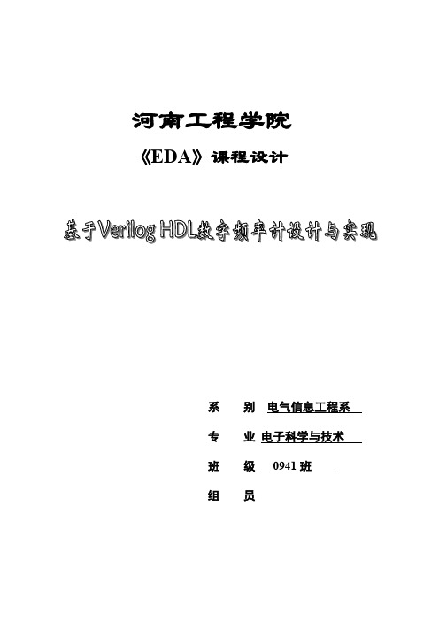
2数字频率计的基本设计原理数字频率计的原理框图如图1所示。
他主要由5个模块组成,分别是:脉冲发生器电路、测频控制信号发生器电路、计数模块电路、锁存器、译码驱动电路。
基于CPLD的频率计设计_毕业设计论文 精品

本科生毕业设计基于CPLD的频率计设计Design of the Frequency Meter based on CPLD学生姓名专业学号指导教师学院毕业设计(论文)原创承诺书1.本人承诺:所呈交的毕业设计(论文)《基于CPLD的频率计设计》,是认真学习理解学校的《长春理工大学本科毕业设计(论文)工作条例》后,在教师的指导下,保质保量独立地完成了任务书中规定的内容,不弄虚作假,不抄袭别人的工作内容。
2.本人在毕业设计(论文)中引用他人的观点和研究成果,均在文中加以注释或以参考文献形式列出,对本文的研究工作做出重要贡献的个人和集体均已在文中注明。
3.在毕业设计(论文)中对侵犯任何方面知识产权的行为,由本人承担相应的法律责任。
4.本人完全了解学校关于保存、使用毕业设计(论文)的规定,即:按照学校要求提交论文和相关材料的印刷本和电子版本;同意学校保留毕业设计(论文)的复印件和电子版本,允许被查阅和借阅;学校可以采用影印、缩印或其他复制手段保存毕业设计(论文),可以公布其中的全部或部分内容。
以上承诺的法律结果将完全由本人承担!作者签名:• 年•• 月•••日摘要频率测量是电子测量领域最基本也是最重要的测量之一。
但基于传统测频原理的频率计在测频时测量精度将随被测信号频率的下降而降低,在实用中有较大的局限性。
因此,本文提出了一种基于CPLD的数字频率计的设计方法。
该设计电路简洁,软件潜力得到充分挖掘,低频段测量精度高,有效防止了干扰的侵入,把CPLD具有的编程灵活,适用范围宽,价格大众化等优点用于实现频率计的设计。
该频率计采用先进的EDA技术及自上而下的设计,使用流行的VHDL语言编程,并在Max+plusII软件平台上进行编译仿真。
经过硬件调试和软件仿真后结果证明此设计方案符合毕设要求和技术参数。
关键词:频率计 EDA技术 CPLDABSTRACTFrequency measurement is the most basic electronic and also one of the most important measure in the measurement field. But the accuracy of frequency meter which is based on the traditional principle will vary depending on the measured signal frequency and the lower, has great limitations in the practical in frequency measurement. Therefore, this article puts forward a design method of digital frequency meter based on CPLD. The advantage such as the CPLD programming flexibility, wide applicable scope, and the popular price etc, are used to implement the frequency meter design by the simple circuit design, the fully excavate of software potential, the precision in low frequency measurement, and the effectively prevent of the invasion of the interference. The frequency meter design which is from top to bottom adopts the advanced EDA technology and popular VHDL language programming, and compiling on Max + plusII software platform simulation.Key words: frequency meter; EDA; CPLD目录摘要 (I)ABSTRACT .......................................................... I I 第1章绪论 .. (1)1.1背景 (1)1.2频率计设计的目的和意义 (1)1.3论文所做的工作及研究内容 (2)第2章设计环境介绍 (3)2.1EDA技术的发展及VHDL简介 (3)2.1.1 EDA技术的发展 (3)2.1.2 VHDL简介 (3)2.1.3 CPLD器件及其特点 (4)2.2基于EDA的CPLD/FPGA设计流程 (4)2.2.1 设计输入 (4)2.2.2 综合 (5)2.2.3 适配 (5)2.2.4 时序仿真与功能仿真 (5)2.2.5 编程下载 (5)2.2.6 硬件测试 (5)2.3M AX+P LUSⅡ开发工具 (6)2.3.1 Max+PlusⅡ开发系统的特点 (6)2.3.2 Max+PlusⅡ的功能 (6)2.3.3 Max+PlusⅡ的设计过程 (6)第3章频率计的设计原理及方案 (8)3.1频率计的设计原理 (8)3.1.1 直接测频法原理 (9)3.1.2 等精度测频法原理 (9)3.2频率计的设计方案 (10)3.2.1 基于直接测频法的设计方案 (10)3.2.2 基于等精度测频法的设计方案 (11)第4章频率计硬件与软件 (14)4.1频率计硬件 (14)4.1.1 电源部分 (14)4.1.2 整形部分 (15)4.1.3 CPLD芯片 (15)4.1.4 显示部分 (16)4.1.5 键盘部分 (17)4.2频率计软件 (18)4.2.1 分频器模块 (18)4.2.2 闸门定时模块 (19)4.2.3 测频控制信号发生器模块 (20)4.2.4 计数器模块 (22)4.2.5 锁存器模块 (23)4.2.6 显示模块 (24)第5章调试 (25)5.1硬件调试 (25)5.1.1 静态调试 (25)5.1.2 连机仿真、在线动态调试 (25)5.2软件调试 (26)参考文献 (28)致谢 (29)附录1 设计源程序 (30)直接测频法 (30)等精度测频法 (33)附录2 电路图 (44)基于CPLD的频率计顶层电路设计图(1)---直接测频法 (44)基于CPLD的频率计顶层电路设计图(2)---等精度测频法 (45)基于CPLD的频率计硬件电路设计图(3)---直接测频法 (46)基于CPLD的频率计硬件电路设计图(4)---等精度测频法 (47)第1章绪论1.1 背景20世纪后期,随着信息技术、电子技术的飞速发展,现代电子产品几乎渗透了社会的各个领域,有力地推动了社会信息化程度的大大提高和社会生产力的发展。
基于FPGA的数字频率计的设计与实现

基于FPGA的频率计的设计和实现金鹏湖北理工学院湖北省黄石市 435000摘要频率计是一种重要的电子测量仪器,本文主要针对使用FPGA(Field Programmable Gate Array)制作一个简单的频率计。
以FPGA(Field Programmable Gate Array)为核心,基于Verilog HDL语言来设计与实现数字频率计。
该频率计具有体积小,性能稳定的特点。
使用FPGA可以顺利设计和实现数字频率计。
关键词:FPGA,频率计,Verilog HDLDesign and implementation of FPGA based on the frequency meterJin pengHubei institute of technology Huangshi city of hubei provinceAbstractFrequency meter is an important electronic measuring instruments, and this article is focused on using FPGA (Field Programmable Gate Array) produced a simple frequency meter. FPGA (Field Programmable Gate Array), design and realization of the digital frequency meter based on Verilog HDL language. The frequency meter has a small size, stable performance characteristics. FPGA can successfully design and implement digital frequency meter.Key words: FPGA, frequency meter, Verilog HDL1总体方案1.1引言频率计又称为频率计数器,频率计最基本的工作原理为:当被测信号在特定时间段T内的周期个数为N时,则被测信号的频率f=N/T。
数字频率计中英文对照外文翻译文献
中英文对照外文翻译文献(文档含英文原文和中文翻译)Introduction of digital frequency meterDigital Frequency is an indispensable instrument of communications equipment, audio and video, and other areas of scientific research and production . In addition to the plastic part of the measured signal, and digital key for a part of the show, all the digital frequency using Verilog HDL designed and implemented achieve in an FPGA chip. The entire system is very lean, flexible and have a modification of the scene.1 、And other precision measuring frequency PrincipleFrequency measurement methods can be divided into two kinds:(1) direct measurement method, that is, at a certain time measurement gate measured pulse signal number.(2) indirect measurements, such as the cycle frequency measurement, VF conversion law. Frequency Measurement indirect measurement method applies only to low-frequency signals.Based on the principles of traditional frequency measurement of the frequency of measurement accuracy will be measured with the decline in signal frequency decreases in the more practical limitations, such as the accuracy and frequency of measurement not only has high accuracy, but also in the whole frequency region to maintain constant test accuracy. The main method of measurement frequency measurement Preferences gated signal GATE issued by the MCU, GATE time width on the frequency measurement accuracy of less impact, in the larger context of choice, as long as the FPGA in 32 of 100 in the counter b M Signals are not overflow line, in accordance with the theoretical calculation GATE time can be greater than the width Tc 42.94 s, but due to the single-chip microcomputer data processing capacity constraints, the actual width of less time, generally in the range of between 0.1 s choice, that is, high-frequency, shorter gate;, low gate longer. This time gate width Tc based on the size of the measured frequency automatically adjust frequency measurement in order to achieve the automatic conversion range, and expanded the range of frequency measurement; realization of the entire scope of measurement accuracy, reduce the low-frequency measurement error.The design of the main methods of measuring the frequency measurement and control block diagram as shown in Figure 1. Figure 1 Preferences gated signal GA TE issued by the MCU, GA TE time width of less frequency measurement accuracy, in the larger context of choice, as long as the FPGA in 32 of 100 in the counter b M signal Overflow will do, according to theoretical calculations GA TE time width T c can be greater than 42194 s, but due to the single-chip microcomputer data processing capacity constraints, the actual width of less time, generally 10 to 011 s in the inter-choice, that is, high - band, the gate time shorter, low gate longer. This time gate width based on the measured T c automatically adjust the size of frequency measurement frequency range to achieve the automatic conversion, and expanded the range of frequency measurement; realization of the entire scope of measurement accuracy, reduce the low-frequency measurement error.2、Frequency of achievingFrequency Measurement accuracy of such method. Can be simplified as shown in the diagram. Map CNT1 and CNT2 two controllable counter, standard frequency (f) signal from the CN F1 clock input cI K input, the signal measured after the plastic (f) CNT2 clock input cI K input. Each counter in the CEN input as enable end, used to control the counter count. When the gate signal is HIGH Preferences (Preferencesstart time). Signal measured by the rising edge of the D flip-flop input, launched at the same time with two counts of juice; Similarly, when preferences for low gate signal (the end of Preferences time), the rising edge of the measured signals through D Trigger output end of the counter to stop counting.3、And the median frequency of relevant indicatorsMedian: At the same time the figures show that up to the median. The usual eight-count frequency of only several hundred yuan can buy. For high precision measurements, nine just beginning, the middle is 11, 13 can be relatively high.Overflow of:-the ability to promote itself to overflow the equivalent of the total. Some of the frequency with overflow function, which is the highest overflow does not display only shows that the bit behind, in order to achieve the purpose of the median. Here is the estimated value of individual indicators.Speed: namely, the number of per second. With the high number of measurement particularly slow but also lose its significance. Counting of the usual eight frequency measurement 10 MHz signals, one second gate will be 10000000 Hz, which is actually seven (equivalent to the median number of common admission after the value), to obtain eight needed 10 seconds gate ; to obtain nine needed 100 seconds gate, followed by analogy, shows that even the permission of 11 need 10,000 second measurement time. But in any case, or seven per second. Therefore, to fast must be a few high speed.Distinction: it is like a minimum voltage meter can tell how much voltage indicators are similar, the smaller the better, unit ps (picoseconds). 1000ps = 1ns. Suppose you use the frequency of 1 ns to differentiate between an e-12 error, we need a ns/1e-12 = 1000 seconds. Also assume that you have a frequency resolution of 100 ps, the measurement time can be shortened by 10 times for 100 seconds, or can be in the same 1000 second measured under an e-14 Error.4、Time and Frequency MeasurementCompared to traditional methods of circuit design, EDA technology uses VHDL language to describe circuit system, including circuit structure, behavior, function and interface logic. Verilog HDL description of a multi-level system hardware functions, and support top-down design features. Designers can not understand the hardware structure. Start from the system design, on the top floor of a system block diagram of the structure and design, in a diagram with Ver-ilog HDL acts on the circuit description and simulation and error correction, and then the system level verification,and finally use logic synthesis optimization tool to create specific gate-level logic circuit netlist, download to the specific FPGA device to in order to achieve FPGA design.Time and frequency measurement is an important area of electronic measurement. Frequency and time measurement has been receiving increasing attention, length, voltage, and other parameters can be transformed into a frequency measurement and related technologies to determine. Based on the more traditional method of synchronization cycle, and has proposed a multi-cycle synchronization and quantitative method of measuring delay frequency method.The most simple method of measuring the frequency of direct frequency measurement method. Direct Frequency Measurement is scheduled to enter the gate signal pulse, the adoption of the necessary counting circuit, the number of pulses are filled to calculate the frequency or analyte signal cycle. In the direct frequency measurement on the basis of the development of multi-cycle synchronous measurement method, in the current frequency monitoring system to be more widely used. Multi-cycle synchronization frequency measurement technology actual gate time is not fixed value, but the measured signals in the whole cycle times, and the measured signal synchronization, thereby removing the measured signal count on when the word ± 1 error, measurement accuracy greatly improved, and reached in the entire spectrum of measurement, such as precision measurement.In the time-frequency measurement method, the multi-cycle synchronization is a high precision, but still unresolved ± a word error, mainly because of the actual gate edge and standard frequency synchronization is not filling pulse edge Tx=N0T0-△t2+△t1, if accurately measured short interval Δ t1 and Δ t2, will be able to accurately measure time intervals Tx, eliminating ± a word counting error, so as to further enhance accuracy.To measure a short time interval Δ t1 and Δ t2, commonly used analog interpolation method with the cursor or more combined cycle synchronization, although accuracy is greatly improved, but eventually failed to resolve ± a word error this fundamental issue, but these methods equipment complex and not conducive to the promotion.To obtain high precision, fast response time, simple structure and the frequency and time measurement method is relatively difficult.Judging from the structure as simple as possible at the same time take intoaccount the point of view of accuracy, multi-cycle synchronization and delay based on the quantitative methods in a short period of time interval measurement, achieved within the scope of broadband, such as high-resolution measurement accuracy.Quantified by measuring short time intervals DelayPhotoelectric signal can be in a certain stability in the medium of rapid spread, and in different media have different delay. By signals generated by the delay to quantify, and gave a short period of time interval measurement.The basic principle is that "delay serial, parallel count", and different from the traditional counter serial number, that is, to signal through a series of delay unit, the delay unit on the delay stability, under the control of the computer Delay on the state of high-speed acquisition and data processing, for a short period of time to achieve accurate measurement interval.Delay quantitative thinking depend on the realization of the delay stability delay unit, the unit depends on the resolution of the delay time delay element.Delay device as a unit can be passive conduit, or other active devices gate circuit. Among them, Traverse shorter delay time (nearly the speed of light transmission delay), the gate delay time longer. Taking into account delays can be predictive ability final choice of the CPLD devices, the realization of the short time interval measurement.Will be the beginning of a short time interval signal sent delay in the transmission chain, when the advent of the end of signal, this signal delay in the delay in the chain latch state, read through the CPU, the judge signal a delay unit on the few short-term time interval can be the size of the unit decided to delay resolution of the unit delay time.Generally speaking, in order to measure both short interval, the use of two modules delay and latches, but in reality, given the time software gate large enough to allow completion from the number of CPU operation, which can be measured in the time interval taken before the end of a short period of time at Δ t1 corresponding delay the number of units through the control signals must be used only a delay and latches units, it saves CPLD internal resources. Synchronization and multi-cycle latency to quantify the method of combining The formula is:T=n0t0+n1t1-n2t1On, n0 for the filling pulse of value; t0 for filling pulse cycle, that is 100 ns; n1 for a short period of time at Δ t1 corresponding delay the number of modules; n2 for ashort period of time at Δ t2 corresponding delay unit Number; t1 quantify delay devices for the delay delay unit volume (4.3 ns). In this way, using multi-cycle synchronization and realized the gate and measured signal synchronization; Delay of using quantitative measurement of the original measured not by the two short intervals, to accurately measure the size of the actual gate, it raised frequency measurement accuracy.The frequency synthesizer output frequency signal can only be transferred to the minimum 10 Hz, XDU-17 as a standard of measurement can be calculated prototype frequency measurement accuracy.For example, the measured signal is measured at 15.000010 MHz MHz signal to 5.00001002, from the calculation can be seen above, the resolution of the prototype has reached ns order of magnitude below from the perspective of theoretical analysis to illustrate this point.It has been anal yzed,multi-cycle synchronization frequency measurement, the measurement uncertainty:When the input f0 10 MHz, 1 s gate time, the uncertainty of measurement of ±1×10⁻⁷/s. When the measurement and quantification of delay circuit with short intervals combined, the uncertainty of measurement can be derived from the following.In the use of cycle synchronization, multi-analyte Tx for the cycle value of T0 time base for the introduction of the cycle.Tx= NT0+△t1-△t2Delay circuit and quantitative combined:Tx= NT0+(N1-N2)td±δTxHere, δTx not for the accuracy of the measurement.On the decline of the share: δTx≤±2tdFrom the details of the measuring accuracy of this method depends on the td, and its direct impact on the stability and size of the uncertainty of measurement. Therefore, the application of methods, counters can be achieved within the entire frequency range, such as the accuracy of measurement, and measurement accuracy is significantly improved, measuring improvement in resolution to 4.3 ns, and the elimination of the word ± a theoretical error, the accuracy is increased by 20 times.CONCLUSION This paper presents a new method of measuring frequency. Based on the frequency of this method of digital integrated circuit in a CPLD, greatlyreduced the volume of the entire apparatus, improved reliability, and a high-resolution measurements.5 、Frequency of VHDL DesignALTERA use of the FPGA chip EPF10K10 companies, the use of VHDL programming language design accuracy of frequency, given the core course. ISPEXPER simulation, design verification is successful, to achieve the desired results. Compared to the traditional frequency of FPGA simplify the circuit board design. Increased system design and the realization of reliability, frequency measurement range of up to 100 MHz and achieve a digital system hardware and software, which is digital logic design the new trend.The design uses the AL TERA EPF10K FPGA chip, the chip pin the delay of 5 ns, frequency of 200 MHz,the standardization of application VHDL hardware description language has a very rich data types, the structure of the model of a complex digital system logic design and computer simulation, and gradually improve after the automatic generation integrated to meet the requirements of the circuit structure of the digital logic can be realized, then can be downloaded to programmable logic devices, to complete design tasks.数字频率计的介绍数字频率计是通信设备、音、视频等科研生产领域不可缺少的测量仪器。
基于VHDL的多功能数字频率计的设计

基于VHDL的多功能数字频率计的设计
随着科技的不断发展,数字频率计作为一种重要的测量仪器在工程领域中得到广泛应用。
本文将介绍一种。
该数字频率计采用VHDL语言进行设计,具有多功能的特点。
首先,该频率计具备高精度的频率测量功能。
通过采用精确的计数方法和高速时钟,能够准确地测量输入信号的频率。
同时,该频率计还具备宽频率范围的测量能力,能够适应不同频率信号的测量需求。
其次,该频率计还具备多种显示方式的功能。
通过设计多种显示模式,用户可以选择不同的显示方式来满足自己的需求。
例如,可以选择数码管显示、LCD显示或者LED显示等方式来显示测量结果。
这样,用户可以根据具体场景和需求选择最合适的显示方式。
此外,该频率计还具备多种触发方式的功能。
通过设计多种触发模式,用户可以选择不同的触发方式来满足自己的需求。
例如,可以选择外部触发、内部触发或者自动触发等方式来触发测量。
这样,用户可以根据具体实验需求选择最合适的触发方式。
最后,该频率计还具备数据存储和传输的功能。
通过设计存储器和通信接口,可以将测量结果存储起来或者传输给其他设备
进行进一步处理。
这样,用户可以方便地保存和分享测量数据,提高工作效率。
综上所述,基于VHDL的多功能数字频率计的设计具有高精度、宽频率范围、多种显示方式、多种触发方式以及数据存储和传输等功能。
该频率计在工程领域中具有重要的应用价值,可以满足不同场景和需求的频率测量需求。
随着科技的不断进步,相信该频率计的设计将能够为工程领域的发展做出积极贡献。
基于VHDL的数字频率计

基于VHDL的数字频率计摘要:本设计分为5个模块:顶层文件程序,十进制计数器模块,4位锁存器模块,控制模块,译码显示模块。
数字频率计是数字电路中的一个典型应用,实际的硬件设计用到的器件较多,连线比较复杂,而且会产生比较大的延时,造成测量误差、可靠性差。
随着复杂可编程逻辑器件(CPLD)的广泛应用,以EDA工具作为开发手段,运用VHDL语言。
将使整个系统大大简化。
提高整体的性能和可靠性。
关键词:频率,VHDL,模块。
目录0.前言 (1)1.系统设计 (1)1.1设计要求 (1)1.1.1设计目的 (1)1.1.2设计内容及要求 (1)1.2总体设计方案 (1)1.2.1设计原理 (1)1.2.2设计框图 (2)1.2.3设计模块说明 (2)2.程序设计 (3)2.1 顶层文件 (3)2.2 十进制计数模块 (3)2.3 4位锁存器模块 (3)2.4 控制模块 (3)2.5 译码显示模块 (4)3.系统仿真 (4)4.结论 (5)5.心得体会 (5)参考文献 (6)附录各模块源程序 (7)0.前言随着时代科技的迅猛发展,微电子学和计算机等现代电子技术的成就给传统的电子测量与仪器带来了巨大的冲击和革命性的影响。
常规的测试仪器仪表和控制装置被更先进的智能仪器所取代,使得传统的电子测量仪器在远离、功能、精度及自动化水平定方面发生了巨大变化,并相应的出现了各种各样的智能仪器控制系统,使得科学实验和应用工程的自动化程度得以显著提高。
数字频率计在电子技术中扮演着一个重要的角色,因此数字频率计是一种最基本的测量仪器,它被广泛应用于航天、电子、测控等领域,许多测量方案和测量结果都与频率有着十分密切的关系,因此频率的测量在电子产品的研究与生产中显得尤为重要。
1.系统设计1.1 设计要求1.1.1设计目的(1)掌握数字频率计的原理、功能、设计与调试方法;(2)熟悉Quartus II的使用方法,学习用VHDL语言编写程序。
基于VHDL的数字频率计的设计

目录引言 (1)第一章概述 (2)1.1 课题研究背景 (2)1.2 国内外概况 (2)1.3 设计概述 (3)1.4 设计内容 (3)1.5 设计原理 (3)1.6 设计功能 (4)第二章技术与开发工具 (5)2.1 VHDL简介 (5)2.1.1 简介 (5)2.1.2 VHDL程序组成部分 (6)2.1.3 VHDL系统优势 (6)2.2 MAX+PLUSⅡ (7)2.2.1 软件简介 (7)2.2.3 软件组成 (8)2.2.4 设计流程 (9)第三章系统分析 (10)3.1数字频率计的设计任务及要求 (10)3.2 模块的划分 (10)3.3设计分析 (11)第四章各功能模块基于VHDL的设计 (12)4.1 时基产生与测频时序控制电路模块的VHDL源程序 (12)4.2 待测信号脉冲计数电路模块的VHDL源程序 (13)4.2.1 十进制加法计数器的VHDL源程序 (13)4.2.2待测信号脉冲计数器的VHDL源程序 (14)4.3 锁存与译码显示控制电路模块的VHDL源程序 (15)4.3.1 译码显示电路的VHDL源程序 (15)4.3.2 锁存与译码显示控制模块的VHDL源程序 (16)4.4 顶层电路的VHDL源程序 (18)第五章数字频率计波形仿真 (20)5.1 时基产生与测频时序控制电路模块的仿真 (20)5.2 待测信号脉冲计数电路模块的仿真 (20)5.2.1 十进制加法计数器的仿真 (20)5.2.2待测信号脉冲计数器的仿真 (21)5.3 锁存与译码显示控制电路模块的仿真 (21)5.3.1 译码显示电路的仿真 (21)5.3.2 锁存与译码显示控制模块的仿真 (22)5.4 数字频率计系统的仿真 (22)结论 (24)致谢................................... 错误!未定义书签。
参考文献.. (25)基于VHDL的数字频率计的设计摘要本文介绍了一种自顶向下分层设计多功能数字频率计的设计方法。
基于CPLD的数字频率计的设计实现
基于 C L P D的 数 字 频 率计 的 设 计 实现
耿兴 隆, 李振川 , 马晓涛
( 北 软 件 职 业技 术 学 院 。 北 保 定 0 10 ) 河 河 7 0 0
摘要 : 频率计是常用的测量仪器 , 它通过对单位 时间内的信 号脉冲进行计 数测量 出信 号的频率。 L tc 用 ai t e公司生产 的
种 , 设 计介 绍 了使 用 一 片 IP S13 本 S L I02芯 片来
2 软 件 设 计
频率计工作时 , 先要产生一个计数允许信号 , 即闸门信号 , 闸门信号的宽度为单位时间, 例如 1 S 或 10m 。 闸门信号有效 的时 间内对被测信号 0 s 在 计数 , 即为信号频率 。 测量过程结束 , 需要锁存计
设 计数 字频率 计 的硬件 电路 和软 件设 计方 法 。 本设 计 为一 个 6位 数 字 频 率 计 , 以 测 量 1 9 9 可 9999
H 的信号频率。 z 设计过程主要分为 : 硬件设计 、 软 件设 计两 部分 。
收稿 日期 :0 0 0 — 2 2 1— 5 1
作者简介 : 耿兴隆(9 2 ) 男, 1 8一 , 河北衡水人 , 助教 , 在读工程硕士 , 要从 事嵌 入式系统、 主 数据 库和计算机控制等方 面的研 究; 李振川(9 0 )男 , 18 一 , 河北 辛集人 , 助教, 主要从事建筑工程 、 计算机 等方面的研 究。
5 2
河 北 软 件 职 业 技 术 学 院 学 报
语言 生成 相应的 目标 文件 , 过下载 电缆将代 码传送 到 目 通 标芯片 中进而完成设计的数字 系统 。 该方法设计灵活 , 便于
实现 。
为 1M z 脉冲发生器芯 片采用 C 4 6 。 D 00 0 h, D 0 0 C 46
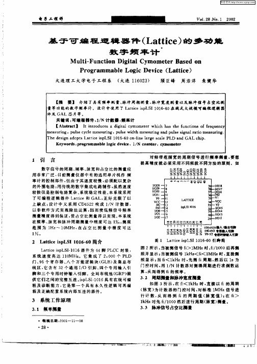
基于可编程逻辑器件(Lattice)的多功能数字频率计
Kc wo d : r g a y r s p o r mma l o i e ie / o n e b elgcd vc ,1 N c u tr,c mo tr y mee
1 引
言
对 频 带 范 围宽 的周 期 信号 进 行 颇事 测量 , 想 要 提 高精度 就 必须采用 不 同频段 不 同方法 的屎则 。如
供它们 之 间 的完整互 连 。 p S 一0 6具有 在线 可编 iLI 1 s 1 程及 诊 断 能力 , 是 第一 个 具有 永 久 性逻 辑 可 再编 它 程及 正确 配置 系统 内部 互连 的器件 。
3 2 周期涓量和脉冲宽度蔼量 .
如 图 3所示 , f l Hz时 , 接 以 f 的周 期 在 i k < 直 i ( 脉宽 ) 为计 数 器 的 门控时 间 , 标 准 1 对 MHz信 号进 行 计 数 , 而 得 到 f 的 周 期 值 ( 宽 值 ) 在 f> 从 i 脉 { i l Hz时先 f 1 0 然 后 进行厨 期 ( 宽) k i 00 / 脉 测量 。
高罱
∞ 1
Y 2 Y I O 5 I I / 4 O IOl / 3
∞ l 2
兰2 昌 高 岛
10 - ̄ / 0I
2 L t c s L I1 1 — O简 介 at eip S 0 66 i
L t c s L I 0 6器 件 为 4 at ei S 一 1 i p 1 4脚 P C 封 装 , L C 系 统 速 度 高 达 n O Hz 它 集 成 了 2 0 0个 P D M 。 ,0 L 门 、 6个 寄 存 器 √ 万 能 逻 辑 块 ( L ) 集 总 布 9 个 G B及 线 区, 含有 3 它 2个 通 用 io 引 脚 、 个 专 用 输 入 引 / 四 脚 和 三 个 专 用 时 钟 输 入 引 脚 。全 局 布 线 池 ( P) GR 提
基于Multisim的高精度数字频率计的设计和仿真
基于Multisim的高精度数字频率计的设计和仿真周敏【摘要】数字频率计是电工电子中常用的测量仪器,数字频率计通过用输入待测信号对一特定长度的信号进行计数,从而得出频率并通过数码管直观的显示出来.本文提出了一种与输入同步的数字频率计的设计,提高了频率计的精度,设计采用Multisim软件进行设计和仿真的过程,介绍了其工作原理,硬件电路设计和仿真的过程.设计采用了Multisim软件进行设计和仿真,设计结果得到的验证.【期刊名称】《机电产品开发与创新》【年(卷),期】2011(024)006【总页数】2页(P95-96)【关键词】频率计;数字电路;Multisim;仿真【作者】周敏【作者单位】华东师范大学苏州工业职业技术学院机电工程系,江苏苏州215104【正文语种】中文【中图分类】TN7020 引言Multisim是一款EDA软件,广泛地应用于电子电路的仿真和设计。
Multisim软件包含丰富的元器件库如74系列等集成电路、电容电阻等基本元件、数码管、51单片机等等,同时还有各种虚拟测量仪器如万用表、示波器、逻辑分析仪等等。
该软件其具有图形化的开发界面,用户只需要选择相应的元器件和测试仪器放置于电路图上,进行连线以后就可以进行仿真,得到直观的仿真结果,大大降低了电路的设计成本,也缩短了产品的开发周期。
数字频率计是电工电子中常用的测量仪器,其原理是对输入信号进行计数,测量其频率并直接通过数码管显示出来。
Multisim非常适合于这类电路的设计和仿真,仿真结果非常的直观和清晰。
文献[1]中采用了Multisim对数字频率计进行了设计和仿真。
本文在这些数字频率计的设计基础上进行了改进,通过跟待测信号同步的时基产生电路将时基信号和待测信号同步,提高了频率计的精度。
同时,本文也采用Multisim工具进行了设计和仿真,验证了设计结果。
1 数字频率计的设计数字频率计的基本原理为通过时基电路产生一个已知长度的信号,将输入信号与这一已知长度信号进行相与,对得到的信号进行计数。
基于复杂可编程逻辑器件的数字频率计的设计与实现外文翻译
Design and Implementation ofDigital Cymometer Based on CPLDAbstractWith the adoption of the top—down design method and AT89C51 SCMC (Single Chip Mico Computer) as the master control component of the system ,the circuit test signalcontrolling ,data operation processing ,keyboard scanning ,and nixie tube display as well were completed by the digital cymometer.ACPLD ,EPM7128SLC84-15 ,programmed by VHDL ,realized various sequence control and count functions 。
The system is characterized by impact structure ,high reliability ,high precision ,and wide frequency-test—range 。
Keywords digital cymometer,complex programmable logic device,SCMC,EDAtechnology1 IntroductionThe system core called SCMC (Single Chip Mico Computer) emerges constantly despite the unceasing development of electronic and computer technologies.The frequency measurement or cycle measurement is usually utilized for testing signals that use frequency as a parameter。
基于VHDL的等精度频率计设计—毕业设计论文
摘要基于传统测频原理的频率计的测量精度将随被测信号频率的下降而降低,在实用中有较大的局限性,本设计采用单片机AT89C51作为主要的控制单元,用来完成电路的信号测试控制、数据运算处理、键盘扫描和控制数码管显示等功能,待测信号经过LM358放大后又经过74HC14形成系统需要的矩形波,然后送入复杂可编程逻辑器件(CPLD),最后由可编程逻辑器件CPLD进行各种时序控制及计数测频功能,并用8位8段LED进行显示。
关键词单片机可编程逻辑器件频率计AbstractBased on the traditional principle of measuring the frequency of the frequency of measurement accuracy will be tested with thefrequency and reduce the decline in the more practical limitations.SCM AT89C51 use this design as the main control unit, the signals used to complete the circuit test control, data processing, keyboard scanning and digital control of the show, and other functions, under test signal LM358 Larger then after a 74 HC14 system needs Rectangular waves, and then into the complex programmable logic devices (CPLD), programmable logic devices by the end CPLD various control and timing count frequency measurement functions, and with eight 8 of the LED display.Keywords: SCMC CPLD Cymometer目录1 引言 (1)1.1课题分析 (1)1.2等精度频率计在国内外发展概况 (1)1.3M AX+P LUS II简介及VHDL语言简介 (3)1.4课题要求 (6)2 等精度频率计的方案选择及原理分析 (7)2.1等精度频率计测频原理 (7)2.2系统原理框图 (9)2.3周期测量 (9)2.4脉冲宽度测量 (10)2.5周期脉冲信号占空比的测量 (10)3 等精度频率计硬件设计 (11)3.1键盘控制模块 (11)3.2显示模块 (12)3.3主控模块 (13)3.4信号输入放大和整形模块 (16)3.5音频输出电路 (17)3.6CPLD功能模块描述 (18)4 等精度频率计软件设计方案 (19)4.1VHDL语言 (19)4.2VHDL软件设计方案 (21)4.3所需VHDL文件及波形仿真结果 (22)4.4单片机的汇编语言编程 (24)5 电路系统调试 (28)6 结论 (29)致谢 (33)附录一:元器件清单 (34)附录二:程序清单 (36)附录三:原理图 (36)1 引言1.1 课题分析在现代电子系统中,数字系统所占的比例越来越大。
- 1、下载文档前请自行甄别文档内容的完整性,平台不提供额外的编辑、内容补充、找答案等附加服务。
- 2、"仅部分预览"的文档,不可在线预览部分如存在完整性等问题,可反馈申请退款(可完整预览的文档不适用该条件!)。
- 3、如文档侵犯您的权益,请联系客服反馈,我们会尽快为您处理(人工客服工作时间:9:00-18:30)。
第34卷第4期2005年12月内蒙古师范大学学报(自然科学汉文版)Journal o f Inner M ongo lia N o rmal U niversit y (Natura l Science Editio n)V ol.34N o.4Dec.2005Received date:2005-05-15Foundation item:Project Supp orted by the Youth Foundation of Inner M ongolia Normal University(QN004009)Biography:GUO Ga-i zh i(1968-),Female,Lecturer of In ner M ongolia Normal Un iversity,M ajor in Dealin g w ith Signal and Information.Design and Implementation ofDigital Cymometer Based on CPLDGU O Ga-i zhi(Col lege of Comp uter and I nf or mation Eng ineer ing ,I nner M ongolia N or mal Univers ity ,H uhhot 010022,China)Abstract :W ith t he ado ption of the to p -dow n design metho d and A T 89C51SCM C (Sing le Chip M ico Comput -er)as t he mast er co ntr ol com ponent o f the sy st em,the cir cuit test signalco ntr olling ,data o per atio n processing ,key -bo ard scanning ,and nixie tube display as w ell w ere co mpleted by the digita l cy mometer.A CPL D,EPM 7128SL C84-15,pr og rammed by VH DL ,r ealized var io us sequence co ntro l and count functions.T he system is characterized byimpact structure,hig h reliability,high precisio n,and w ide frequency -test -range.Key words :dig ital cy mometer;complex pr og rammable log ic dev ice;SCM C;EDA technolog yCLC number :T P 273 Document code :A A rticle ID :1001--8735(2005)04--0434--041 Int roductionThe sy stem core called SCM C(Sing le Chip M ico Computer)em erg es constantly despite the unceasing development o f electr onic and com puter technolo gies.T he frequency m easurement or cycle measurement is usually utilized for testing signals that use frequency as a parameter.When the tested frequency is relativ ely hig h,relatively hig h pr ecision can be available w ith frequency m easurement.When the tested frequency is relatively low ,relativ ely hig h precision can be available w ith cy cle measurement.H ow ever,neither of them can ensur e the m easurement precision in the w ho le frequency rang e,w hen the range o f tested frequency is com paratively w ide.This digital Cym ometer utilizes the adv anced EDA technolog y and top -dow n desig n method.T hus,the Cy no meter implem ents the equal precision m easurement of the sig nal frequency rang e of 0.1H z~50MH z by A T89C 51SCMC and CPLD,and also m easures pulse w idth and duty ratio.Because of the co nv enience of CPLD prog ramming,quick speed,hig h integr ation,and low price,the sy stem research circle is ex tr em ely shortened and the pr oduct ratio of perfo rmance ver sus price is improved.The CPLD chip employs the popu -lar VH DL and achiev es all the progr am desig n and Dow nload on the M AX+PlusII softw are platform.The control po rtio n of SCM C,pr ogram med by assemble lang uag e precisely sets tim e,ex actly contr ols startup and closedo w n o f frequency -test count str obe,w hich further ensur es measurement precision.System theory and so ftw are &hardw are design are introduced below.2 Equal precision m easurement theoryIn CPLD,to p -lev el circuit structure realized by VH DL is show n in fig ure 1,w here CONT ROL 1is con -tro l m odule of frequency -test,CONTROL 2is contro l module of pulse -w idth -test and duty r atio,CH OICE is choice mo dule o f self -adjustm ent and measur em ent;COU NT is count m odule of datum frequency and fre -quency -test.Under the contr ol o f SCM C,the CPLD accom plishes fr equency -test in the follow ing steps:第4期郭改枝:基于复杂可编程逻辑器件的数字频率计的设计与实现(a)Plus pulse signal is added at CLR,thereby com pleting the initialization of testing circuit state (w hen frequency is tested,CS,AS is low ,ED 2is irrelev ant).(b)When stro be sig nal STROBE is set hig h,tim ing starts.M eanw hile,r ising edg e of pulse -test signal Fx ,which is selected by CH OICE mo dule,initiates frequency -test contr ol mo dule CONT ROL 1,w hich makes tw o sets o f 32-bit counter w ithin COU NT take count of datum frequency signal F s and signa-l test Fx synchro nously.(c)STROBE is set low w hen stro be timing ends.COU NT stops counting once r ising edg e of nex t pulse of sig na-l test advents.(d)After co unt finishes,ED 1outputs low level to apply for interr upt fro m SCM C.In the Inter rupt Serv ice Ro utine,SCM C reads co unt value of datum frequency signal and signa-l test in COUNT fro m port P 0and P 2of SCM C for fo ur tim es,through encoding address line SS 1and SS 0.If the count value of signa-l test is N x ,datum frequency p s is N s ,then Fx =(Fs/N s)N x .F ig.1 Fr equency measurement top -level module3 Design of system hardw are circuitThe block diagram of system hardw are circuit is sho w n in figure 2.There is a 4kB Flash Memo ry in AT89C51SCMC into w hich all contr ol pr ogram can be stored.SCM C w rites the result tested from CPLD each time into RAM ,and then sends it in decim al into eight -bit nixie tube display circuit to display after operation processing.Keyboard co ntro l co mmand is w ritten into SCM C via a 74LS 165,Parallel in/Serial Output Shift Registers.SCM C utilizes one 12M H z cry stal w hose oscilla -tion pulse is serv ed as self -adjustment input of CPLD at the same time.Signa-l test is inputted to CPLD via w ide band amplify and Schmitt cir cuit shape.50M H z activ e cry stal m odule is used for datum frequencyinput.Fig.2 Sy stem blo ck diag ram#435#内蒙古师范大学学报(自然科学汉文版)第34卷 4 V H DL program desig nCPLD softw are prog ram is achieved by VH DL.A portion of top -level module prog ram is as follow :LIBRARY IEEE;USE IEEE.STD_LOGIC_1164.ALL;USE IEEE.STD_LOGIC_UNSIGNED.ALL;EN TITY FREQUENCY 8ISPORT (SS 0,SS 1,FS,FX,FC,CLR,AS,ST ROBE,CS:IN ST D_LOGIC;ED 1,ED 2:OUT STD_LOGIC;B:OU T ST D_LOGIC_V ECT OR (15DOWNTO 0));END FREQU EN CY 8;ARCH ITECTU RE RT L OF FREQU ENCY 8ISSIGNAL FX 0,CLKX,CLKS,CLE,SSL1:STD_LOGIC;,,COM PONENT COU NTPORT (FX 1,FS 1,CLR,SS 0,SS 1:IN STD_LOGIC;B:OU T ST D_LOGIC_V ECT OR (15DOWNTO 0));END COM PONENT;BEGINU 1:CH OICE PORT M AP(FX=>FX,FC=>FC,A S=>AS,FOUT =>FX 0);U 2:CONTROL 1PORT M AP(FX 1=>FX 0,STROBE=>ST ROBE,CLR=>CLR,FS=>FS,CS=>CS,SSL=>SSL 1,CLK 1=>CLKX,CLK 2=>CLKS,CLRC=>CLE,ED 1=>ED 1);U 3:CONTROL 2PORT M AP(FIN=>FX 0,ST ROBE=>ST ROBE,CLR=>CLR,SSL=>SSL 1,ED 2=>ED 2);U 4:COUNT PORT MA P(FX1=>CLKX,FS 1=>CLKS,CLR=>CLE,SS 0=>SS 0,SS 1=>SS 1,B=>B);END RTL;Figure 3is the em ulation w aveform diag ram w hen sig na-l test Fx =10MH z and F s =50M Hz.F ig.3 Emulation wav eform diag ram#436#第4期郭改枝:基于复杂可编程逻辑器件的数字频率计的设计与实现 5 Frequency -test precision analy sisFro m the frequency -test formula:Fx =(Fs/N s)N x .Suppose that frequency -test is Fx ,its true v alue is Fx e ,and standar d frequency is F s .In one m easurement,because Fx count startup and closedow n tim e are bo th tr ig gered by the signal p s rising edge,count N x of F x has no erro r in one strobe time T ,w hile co unt N s has error of o ne pulse at most,that is |$et |[1,w e can derived Fx e =(F s/(N s +v et))N x from Fx /N x =Fs/N s and Fx e/N x =Fs/(N s +$et ).According to relative err or for mula $Fx e/F x e =|Fx e -Fx |/Fx e ,w e have $F x e/Fx e =|$et |/N s .T hen,since |$et |[1,w e o btain |$et |/N s [1/N s,N s =T Fs .Accordingly w e reach the conclusio n that relative m easurement err or has no relation to frequency -test,measurem ent erro r w hich can be r educed and measur em ent precision im pro ved v ia aug menting strobe time T or enhancing F s .The measurement precisio n o f frequency -test system remains co nstant in the entire fre -quency range in case that strobe tim e and general frequency m easurement strobe time is uniform and sig na-l test fr equency is dissimilar.The range of this sy stem fr equency -test is set as fr om 0.1H z to 50M H z.Strobe tim e is set to tw o grades:1s and 10s.T he stro be can test and obtain sig nal once every 10s w hen frequency -test is 0.1H z.50MH z upper limit frequency setting depends o n such factor s as inter nal counter digit of CPLD,CPLD clock,nix ie tube dig it,and so on.In 10s stro be time,50M H z datum frequency can count 500M H z pulse (only 29bits binary number r equired),while 400MH z can be counted in theory as the 32-bit of signa-l test is fully used in 10s.H o w ever,because it is limited by tw o sets of global co unt clo ck,w hich is 151.5M H z at most,in EPM 7128SLC 84-15chip selected by the sy stem and the digit of 8-bit nixie tube,the upper limit frequency is r estr icted w ithin 50MH z.In that case,frequency -test w hole -rang e relative error is m illio nth constantly.References:[1] Song Pan,Guodong Wang.V H DL A pplication Cour se [M ].Chengdu:U niv ersity of Electro nic Science and T echno lo gyP ress,2000.[2] Wanjie Song,Ping Luo,Shunjun Wu.CPL D T echno lo gy and A pplication [M ].Xi p an:Xi p an U niversit y of Elect ronic Sc-ience and T echnolo gy Pr ess,2000.[3] Bo heng Ho u,Xin G u.V HD L Har dw are D escr iption L anguage and Digit al L og ic Circuit Desig n [M ].X i p an:Xi p an U n-iversity o f Electro nic Science and T echno log y P ress,2001.基于复杂可编程逻辑器件的数字频率计的设计与实现郭改枝(内蒙古师范大学计算机与信息工程学院,内蒙古呼和浩特010022)摘 要:采用自上向下的设计方法,设计了基于复杂可编程逻辑器件的数字频率计.以A T 89C51单片机作为系统的主控部件,完成电路的测试信号控制、数据运算处理、键盘扫描和控制数码管显示.用V H DL 语言编程,由CPL D(Co mplex Pro gr ammable L og ic Device)EP M 7128SL C 84-15完成各种时序控制及计数功能.该系统具有结构紧凑、可靠性高、测频范围宽和精度高等特点.关键词:数字频率计;逻辑器件;单片机;EDA 技术中图分类号:T P 273 文献标识码:A 文章编号:1001--8735(2005)04--0434--04【责任编辑陈汉忠】#437#。