FPGA可编程逻辑器件芯片AD823AARZ-R7中文规格书
FPGA可编程逻辑器件芯片XC7A50T-2FGG484I中文规格书
IntroductionArtix®-7 FPGAs are available in -3, -2, -1, -1LI, and -2L speed grades, with -3 having the highest performance. The Artix-7FPGAs predominantly operate at a 1.0V core voltage. The -1LI and -2L devices are screened for lower maximum static power and can operate at lower core voltages for lower dynamic power than the -1 and -2 devices, respectively. The -1LI devices operate only atV CCINT =V CCBRAM =0.95V and have the same speed specifications as the -1 speed grade. The -2L devices can operate at either of two V CCINT voltages, 0.9V and 1.0V and are screened for lower maximum static power. Whenoperated at V CCINT =1.0V, the speed specification of a -2L device is the same as the -2 speed grade. When operated at V CCINT =0.9V, the -2L static and dynamic power is reduced.Artix-7 FPGA DC and AC characteristics are specified in commercial, extended, industrial, expanded (-1Q), and military (-1M) temperature ranges. Except the operating temperature range or unless otherwise noted, all the DC and AC electrical parameters are the same for a particular speed grade (that is, the timing characteristics of a -1Mspeed grade military device are the same as for a -1C speed grade commercial device). However, only selected speed grades and/or devices are available in each temperature range. For example, -1M is only available in thedefense-grade Artix-7Q family and -1Q is only available in XA Artix-7FPGAs.All supply voltage and junction temperature specifications are representative of worst-case conditions. The parameters included are common to popular designs and typical applications.Available device and package combinations can be found in :•7Series FPGAs Overview (DS180)•Defense-Grade 7Series FPGAs Overview (DS185)•XA Artix-7 FPGAs Overview (DS197)DC CharacteristicsTable 1:Absolute Maximum Ratings (1)SymbolDescription Min Max UnitsFPGA Logic V CCINT Internal supply voltage –0.5 1.1V V CCAUX Auxiliary supply voltage–0.5 2.0V V CCBRAM Supply voltage for the block RAM memories –0.5 1.1V V CCO Output drivers supply voltage for HR I/O banks –0.5 3.6V V REF Input reference voltage –0.5 2.0V V IN (2)(3)(4)I/O input voltage–0.4V CCO +0.55V I/O input voltage (when V CCO =3.3V) for V REF and differential I/O standards except TMDS_33(5)–0.4 2.625V V CCBATTKey memory battery backup supply–0.52.0VGTP Transceiver V MGTAVCC Analog supply voltage for the GTP transmitter and receiver circuits–0.5 1.1V V MGTAVTT Analog supply voltage for the GTP transmitter and receiver termination circuits –0.5 1.32V V MGTREFCLK Reference clock absolute input voltage–0.5 1.32V V INReceiver (RXP/RXN) and Transmitter (TXP/TXN) absolute input voltage–0.51.26V找FPGA ,上赛灵思半导体(深圳)有限公司I DCIN-FLOAT DC input current for receiver input pins DC coupled RX termination =floating –14mA I DCIN-MGTAVTT DC input current for receiver input pins DC coupled RX termination =V MGTAVTT –12mA I DCIN-GND DC input current for receiver input pins DC coupled RX termination =GND – 6.5mA I DCOUT-FLOAT DC output current for transmitter pins DC coupled RX termination =floating –14mA I DCOUT-MGTAVTTDC output current for transmitter pins DC coupled RX termination =V MGTAVTT –12mA XADC V CCADC XADC supply relative to GNDADC –0.5 2.0V V REFPXADC reference input relative to GNDADC–0.52.0VTemperature T STG Storage temperature (ambient)–65150°C T SOL Maximum soldering temperature for Pb/Sn component bodies (6)–+220°C Maximum soldering temperature for Pb-free component bodies (6)–+260°C T j Maximum junction temperature (6)–+125°CNotes:1.Stresses beyond those listed under Absolute Maximum Ratings might cause permanent damage to the device. These are stress ratings only, and functional operation of the device at these or any other conditions beyond those listed under Operating Conditions is not implied.Exposure to Absolute Maximum Ratings conditions for extended periods of time might affect device reliability.2.The lower absolute voltage specification always applies.3.For I/O operation, refer to 7Series FPGAs SelectIO Resources User Guide (UG471).4.The maximum limit applies to DC signals. For maximum undershoot and overshoot AC specifications, see Table 4.5.See Table 9 for TMDS_33 specifications.6.For soldering guidelines and thermal considerations, see 7Series FPGA Packaging and Pinout Specification (UG475).Table 2:Recommended Operating Conditions (1)(2)Symbol Description Min Typ Max UnitsFPGA LogicV CCINT (3)For -3, -2, -2LE (1.0V), -1, -1Q, -1M devices: internal supply voltage0.95 1.00 1.05V For -1LI (0.95V) devices: internal supply voltage 0.920.950.98V For -2LE (0.9V) devices: internal supply voltage 0.870.900.93V V CCAUX Auxiliary supply voltage1.71 1.80 1.89V V CCBRAM (3)For -3, -2, -2LE (1.0V), -2LE (0.9V), -1, -1Q, -1M devices: block RAM supply voltage0.95 1.00 1.05V For -1LI (0.95V) devices: block RAM supply voltage 0.920.950.98V V CCO (4)(5)Supply voltage for HR I/O banks 1.14– 3.465V V IN (6)I/O input voltage–0.20–V CCO +0.20V I/O input voltage (when V CCO =3.3V) for V REF and differential I/O standards except TMDS_33(7)–0.20– 2.625V I IN (8)Maximum current through any pin in a powered or unpowered bank when forward biasing the clamp diode.––10mA V CCBATT (9)Battery voltage1.0–1.89VGTP TransceiverV MGTAVCC (10)Analog supply voltage for the GTP transmitter and receiver circuits0.97 1.0 1.03V V MGTAVTT (10)Analog supply voltage for the GTP transmitter and receiver termination circuits1.171.21.23VXADC V CCADCXADC supply relative to GNDADC1.711.801.89VTable 1:Absolute Maximum Ratings (1) (Cont’d)Symbol DescriptionMin Max UnitsTable 3:DC Characteristics Over Recommended Operating ConditionsSymbolDescriptionMin Typ (1)Max Units V DRINT Data retention V CCINT voltage (below which configuration data might be lost)0.75––V V DRI Data retention V CCAUX voltage (below which configuration data might be lost) 1.5––V I REF V REF leakage current per pin––15µA I L Input or output leakage current per pin (sample-tested)––15µA C IN (2)Die input capacitance at the pad––8pF I RPU Pad pull-up (when selected) @ V IN =0V, V CCO =3.3V 90–330µA Pad pull-up (when selected) @ V IN =0V, V CCO =2.5V68–250µA Pad pull-up (when selected) @ V IN =0V, V CCO =1.8V 34–220µA Pad pull-up (when selected) @ V IN =0V, V CCO =1.5V 23–150µA Pad pull-up (when selected) @ V IN =0V, V CCO =1.2V12–120µA I RPD Pad pull-down (when selected) @ V IN =3.3V68–330µA I CCADC Analog supply current, analog circuits in powered up state ––25mA I BATT (3)Battery supply current––150nA R IN_TERM (4)Thevenin equivalent resistance of programmable input termination to V CCO /2 (UNTUNED_SPLIT_40)284055ΩThevenin equivalent resistance of programmable input termination to V CCO /2 (UNTUNED_SPLIT_50)355065ΩThevenin equivalent resistance of programmable input termination to V CCO /2 (UNTUNED_SPLIT_60)446083ΩDIFF_SSTL18_II0.3000.9001.4250.100–(V CCO /2)–0.600(V CCO /2)+0.60013.4–13.4Notes:1.V ICM is the input common mode voltage.2.V ID is the input differential voltage (Q –Q).3.V OL is the single-ended low-output voltage.4.V OH is the single-ended high-output voltage.Table 10:Complementary Differential SelectIO DC Input and Output Levels (Cont’d)I/O Standard V ICM (1)V ID (2)V OL (3)V OH (4)I OL I OH V, Min V,Typ V, Max V,Min V, MaxV, Max V, Min mA, Max mA, MinAC Switching CharacteristicsAll values represented in this data sheet are based on the speed specifications from the ISE® Design Suite and Vivado®Design Suite as outlined in Table12.Table 12:Artix-7 FPGA Speed Specification Version By DeviceVersion In:Typical V CCINTDeviceISE 14.7Vivado 2018.2(Table2)N/A 1.22 1.0V XC7A12T, XC7A15T, XC7A25T, XC7A35T, XC7A50T, XC7A75TN/A 1.220.95V XC7A12T, XC7A15T, XC7A25T, XC7A35T, XC7A50T, XC7A75T, XC7A100T,XC7A200TN/A 1.140.9V XC7A12T, XC7A15T, XC7A25T, XC7A35T, XC7A50T, XC7A75T1.10 1.22 1.0V XC7A100T, XC7A200T1.07 1.140.9V XC7A100T, XC7A200TN/A 1.15 1.0V XA7A12T, XA7A15T, XA725T, XA7A35T, XA7A50T, XA7A75T1.07 1.15 1.0V XA7A100T1.06 1.11 1.0V XQ7A100T, XQ7A200TN/A 1.11 1.0V XQ7A50T。
FPGA可编程逻辑器件芯片EP4CE40F23I7N中文规格书
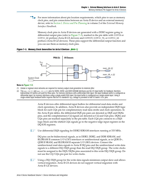
Chapter 7:External Memory Interfaces in Arria II DevicesMemory Interfaces Pin Support for Arria II Devicesf For more information about pin location requirements, which pins to use as memoryclock pins, and pin connections between an Arria II device and an external memorydevice, refer to Section I. Device and Pin Planning in volume 2 of the External MemoryInterface Handbook.Memory clock pins in Arria II devices are generated with a DDIO register going todifferential output pins (refer to Figure7–3), marked in the pin table with DIFFIN orDIFFIO_RX prefixes (Arria II GX devices) and DIFFOUT, DIFFIO_TX, or DIFFIO_RXprefixes (Arria II GZ devices). These pins support the differential output function andyou can use them as memory clock pins.Figure7–3.Memory Clock Generation for Arria II Devices(Note1)Notes to Figure7–3:(1)Global or regional clock networks are required for memory output clock generation to minimize jitter.(2)The mem_clk[0] and mem_clk_n[0] pins for DDR3, DDR2, and DDR SDRAM interfaces use the I/O input buffer for feedback; therefore,bidirectional I/O buffers are used for these pins. For memory interfaces with a differential DQS input, the input feedback buffer is configured as differential input; for memory interfaces using a single-ended DQS input, the input buffer is configured as a single-ended input. Using a single-ended input feedback buffer requires that the I/O standard’s V REF voltage is provided to that I/O bank’s VREF pins.Arria II devices offer differential input buffers for differential read-data strobe andclock operations. In addition, Arria II devices also provide an independent DQS logicblock for each CQn pin for complementary read-data strobe and clock operations. Inthe Arria II pin tables, the differential DQS pin pairs are denoted as DQS and DQSnpins, and the complementary CQ signals are denoted as CQ and CQn pins. DQSn andCQn pins are marked separately in the pin table. Each CQn pin connects to a DQSlogic block and the shifted CQn signals go to the negative-edge input registers in theDQ IOE registers.1Use differential DQS signaling for DDR2 SDRAM interfaces running at 333MHz.DQ pins can be bidirectional signals, as in DDR3, DDR2, and DDR SDRAM, andRLDRAM II common I/O (CIO) interfaces or unidirectional signals, as in QDR II+,QDR II SRAM, and RLDRAM II separate I/O (SIO) devices. Connect theunidirectional read-data signals to Arria II DQ pins and the unidirectional write-datasignals to a different DQ/DQS group than the read DQ/DQS group. The write clocksmust be assigned to the DQS/DQSn pins associated to this write DQ/DQS group. Donot use the CQ/CQn pin-pair for write clocks.1Using a DQ/DQS group for the write-data signals minimizes output skew and allows vertical migration. Arria II GX devices do not support vertical migration withArria II GZ devices.Arria II Device Handbook Volume 1: Device Interfaces and IntegrationChapter 6:I/O Features in Arria II DevicesTermination Schemes for I/O Standardsmini-LVDSArria II GX devices support true mini-LVDS with a three-resistor network using twosingle-ended output buffers for external three-resistor networks.For Arria II GZ devices, use two single-ended output buffers with external one- orthree-resistor networks (mini-LVDS_E_1R or mini-LVDS_E_3R). Arria II GZ row I/Obanks support mini-LVDS output using true LVDS output buffers without an externalresistor network.Figure6–18 shows the one-resistor and three-resistor topology for RSDS andmini-LVDS I/O standard termination.Figure6–18.RSDS and mini-LVDS I/O Standard Termination for Arria II Devices(Note1)Notes to Figure6–18:(1)R p = 170 Ω and R s= 120 Ω(2)mini-LVDS_E_1R is applicable for Arria II GZ devices only.A resistor network is required to attenuate the LVDS output-voltage swing to meetRSDS and mini-LVDS specifications. You can modify the three-resistor networkvalues to reduce power or improve the noise margin. The resistor values chosenshould satisfy the equation shown in Equation6–1.Equation6–1.Resistor Network1To validate that custom resistor values meet the RSDS requirements, Alterarecommends performing additional simulations with IBIS models.f For more information about the RSDS I/O standard, refer to the RSDS Specificationfrom the National Semiconductor website at .f For more information about the mini-LVDS I/O standard, see the mini-LVDSSpecification from the Texas Instruments website at .Arria II Device Handbook Volume 1: Device Interfaces and IntegrationChapter 6:I/O Features in Arria II DevicesArria II OCT CalibrationArria II OCT CalibrationArria II GX devices support calibrated R S OCT and Arria II GZ devices supportcalibrated R S and R T OCT on all I/O pins. You can calibrate the I/O banks with any ofthe OCT calibration blocks available in the device provided the V CCIO of the I/O bankwith the pins using calibrated OCT matches the V CCIO of the I/O bank with thecalibration block and its associated RUP and RDN pins.f For more information about the location of the OCT calibration blocks in Arria IIdevices, refer to the Arria II Device Family Connection Guidelines and Arria II DevicePin-Outs.OCT Calibration BlockAn OCT calibration block has the same V CCIO as the I/O bank that contains the block.R S OCT calibration is supported on all user I/O banks with different V CCIO voltagestandards, up to the number of available OCT calibration blocks. You can configureI/O banks to receive calibrated codes from any OCT calibration block with the sameV CCIO. All I/O banks with the same V CCIO can share one OCT calibration block, even ifthat particular I/O bank has an OCT calibration block.For example, Figure6–10 shows a group of I/O banks that has the same V CCIOvoltage. If a group of I/O banks has the same V CCIO voltage, you can use one OCTcalibration block to calibrate the group of I/O banks placed around the periphery.Because banks 3B, 4C, 6C, and 7B have the same V CCIO as bank 7A, you can calibrateall four I/O banks (3B, 4C, 6C, and 7B) with the OCT calibration block (CB7) locatedin bank 7A. You can enable this by serially shifting out R S OCT calibration codes fromthe OCT calibration block located in bank 7A to the I/O banks located around theperiphery.1I/O banks that do not contain calibration blocks share calibration blocks with I/O banks that do contain calibration blocks.Arria II Device Handbook Volume 1: Device Interfaces and Integration。
FPGA可编程逻辑器件芯片XC7Z020-2CLG400I中文规格书

FPGA Mezzanine (FMC) Card Interface[Figure1-2, callout 24]The ZC702 board supports the VITA 57.1 FPGA Mezzanine Card (FMC) specification [Ref6] by providing subset implementations of low pin count (LPC) connectors at J3 and J4. Both connectors use a 10x40 form factor that is partially populated with 160 pins. Theconnectors are keyed so that a the mezzanine card faces away from the ZC702 board when connected.Connector Type:•Samtec SEAF series, 1.27 mm (0.050 in) pitch. Mates with SEAM series connector.For more information about SEAF series connectors, go to the Samtec website [Ref28].LPC Connectors J3 and J4[Figure1-2, callout 24]The 160-pin FMC LPC connector is shown in Figure B-1.The LPC connections between FMC1 (J3) and XC7Z020 SoC U1 (Table1-28) and between FMC2 (J4) and XC7Z020 SoC U1 (Table1-29) both implement a subset of this connectivity (GTX is not supported):•68 single-ended or 34 differential user-defined signals (34 LA pairs, LA00–LA33)•0GTX transceivers•0GTX clocks• 2 differential clocks•61 ground and 9 power connectionsNote:FMC1 (J3) and FMC2 (J4) GA0 = GA1 = 0 (GND).Table1-28 shows the LPC connections between J3 and XC7Z020 SoC U1.Table 1-28:LPC Connections, FMC1 (J3) to XC7Z020 SoC U1FMC1J3 Pin Net NameI/OStandardXC7Z020(U1) PinFMC1J3 Pin Net NameI/OStandardXC7Z020(U1) PinC2NC D1PWRCTL2_VCC4A_PGC3NC D4NCC6NC D5NCC7NC D8FMC1_LPC_LA01_CC_P LVCMOS25N19 C10FMC1_LPC_LA06_P LVCMOS25J18D9FMC1_LPC_LA01_CC_N LVCMOS25N20 C11FMC1_LPC_LA06_N LVCMOS25K18D11FMC1_LPC_LA05_P LVCMOS25N17The ZC702 board uses power regulators and a PMBus compliant system controller from Texas Instruments to supply core and auxiliary voltages as listed in Table1-30. The Texas Instruments Fusion Digital Power graphical user interface is used to monitor the voltage and current levels of the board power modules.Table 1-30:Onboard Power System DevicesDevice Type ReferenceDesignator Description Power RailNet NamePower RailVoltageSchematicPageCore voltage controller and regulatorsUCD9248PFCU32PMBus Controller–CoreAddr = 52 dec., 0b0110100)39PTD08D210W—VoutAU17Dual 10A 0.6V–3.6V Adj. SwitchingRegulatorVCCINT 1.00V40PTD08D210W—VoutB Dual 10A 0.6V–3.6V Adj. SwitchingRegulatorVCCPINT 1.00V40PTD08D210W—VoutAU18Dual 10A 0.6V–3.6V Adj. SwitchingRegulatorVCCAUX 1.80V41PTD08D210W—VoutB Dual 10A 0.6V–3.6V Adj. SwitchingRegulatorVCCPAUX 1.80V41 Auxiliary voltage controller and regulatorsUCD9248PFCU33PMBus Controller–AuxAddr = 53 dec., 0b0110101)42PTD08D210W—VoutAU19Dual 10A 0.6V–3.6V Adj. SwitchingRegulator(set to 1.8V, 2.5V or 3.3V)VADJ 2.50V43PTD08D210W—VoutB Dual 10A 0.6V–3.6V Adj. SwitchingRegulatorVCC1V5 1.50V43PTD08D210W—VoutAU20Dual 10A 0.6V–3.6V Adj. SwitchingRegulatorVCCMIO_PS 1.80V44PTD08D210W—VoutB Dual 10A 0.6V–3.6V Adj. SwitchingRegulatorVCCBRAM 1.00V44UCD9248PFCU34PMBus Controller–AuxAddr = 54 dec., 0b0110110)45PTD08D210W—VoutAU21Dual 10A 0.6V–3.6V Adj. SwitchingRegulatorVCC3V3 3.30V46PTD08D210W—VoutB Dual 10A 0.6V–3.6V Adj. SwitchingRegulatorVCC2V5/VCC2V5_PL 2.50V46Linear regulatorTPS51200DR U223A Tracking Regulator VTTDDR_PS0.75V37internally OR's these PG conditions together and drives an output PG pin High only if all active rail PG states are “good”. The On and Off Delay and rise and fall times are relative to when the board power on-off slide switch SW12 is turned on and off.Table1-31 defines the voltage and current values for each power rail controlled by theUCD9248 PMBus controller at address 52 decimal (U32).Table 1-31:Power Rail Specifications for UCD9248 PMBus Controller at Address 52 DecimalShutdown Threshold(1)Rail NumberRailName Rail NameNominalVOUT(V)PGOnThreshold(V)PGOffThreshold(V)OnDelay(ms)RiseTime(ms)OffDelay(ms)FallTime(ms)VOUTOverFault(V)IOUTOverFault(A)TempOverFault(°C)1Rail #1VCCINT10.90.8505101 1.152090 2Rail #2VCCPINT10.90.8505101 1.152090 3Rail #3VCCAUX 1.8 1.62 1.530551 2.0710.4190 4Rail #4VCCPAUX 1.8 1.62 1.530551 2.0710.4190Table1-33 defines the voltage and current values for each power rail controlled by the UCD9248 PMBus controller at address 54 decimal (U34).Table 1-33:Power Rail Specifications for UCD9248 PMBus Controller at Address 54 DecimalShutdown Threshold(1)Rail NumberRailNameSchematicRail NameNominalVOUT(V)PGOnThreshold(V)PGOffThreshold(V)OnDelay(ms)RiseTime(ms)OffDelay(ms)FallTime(ms)VOUTOverFault(V)IOUTOverFault(A)TempOverFault(°C)1Rail #1VCC3V3 3.3 2.97 2.8050541 3.79510.4190 2Rail #2VCC2V5 2.5 2.25 2.1250511 2.87510.4190 Notes:1.The values defined in these columns are the voltage, current, and temperature thresholds that causes the regulator to shut。
FPGA可编程逻辑器件芯片EP4CE55F23C7N中文规格书
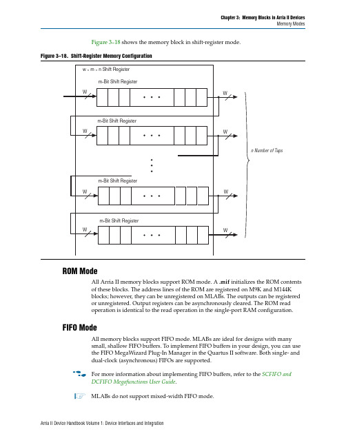
Chapter 3:Memory Blocks in Arria II DevicesMemory Modes Figure3–18 shows the memory block in shift-register mode.Figure3–18.Shift-Register Memory ConfigurationROM ModeAll Arria II memory blocks support ROM mode. A .mif initializes the ROM contentsof these blocks. The address lines of the ROM are registered on M9K and M144Kblocks; however, they can be unregistered on MLABs. The outputs can be registeredor unregistered. Output registers can be asynchronously cleared. The ROM readoperation is identical to the read operation in the single-port RAM configuration.FIFO ModeAll memory blocks support FIFO mode. MLABs are ideal for designs with manysmall, shallow FIFO buffers. To implement FIFO buffers in your design, you can usethe FIFO MegaWizard Plug-In Manager in the Quartus II software. Both single- anddual-clock (asynchronous) FIFOs are supported.f For more information about implementing FIFO buffers, refer to the SCFIFO andDCFIFO Megafunctions User Guide.1MLABs do not support mixed-width FIFO mode.Arria II Device Handbook Volume 1: Device Interfaces and IntegrationChapter 9:Configuration, Design Security, and Remote System Upgrades in Arria II DevicesJTAG ConfigurationYou must connect the nCE pin to GND or drive it low during JTAG configuration. Inmulti-device FPP, AS, and PS configuration chains, the nCE pin of the first device isconnected to GND, while its nCEO pin is connected to nCE of the next device in thechain. The nCE input of the last device comes from the previous device, while its nCEOpin is left floating. In addition, the CONF_DONE and nSTATUS signals are all shared inmulti-device FPP, AS, or PS configuration chains so the devices can enter user mode atthe same time after configuration is complete. When the CONF_DONE and nSTATUSsignals are shared among all the devices, you must configure every device when JTAGconfiguration is performed.1If you only use JTAG configuration, Altera recommends connecting the circuitry as shown in Figure9–17, where each of the CONF_DONE and nSTATUS signals are isolated toenable each device to enter user mode individually.After the first device completes configuration in a multi-device configuration chain,its nCEO pin drives low to activate the nCE pin of the second device, which prompts thesecond device to begin configuration. Therefore, if these devices are also in a JTAGchain, ensure the nCE pins are connected to GND during JTAG configuration or thatthe devices are JTAG configured in the same order as the configuration chain. As longas the devices are JTAG configured in the same order as the multi-deviceconfiguration chain, the nCEO of the previous device drives the nCE of the next devicelow when it has successfully been JTAG configured.You can place other Altera devices that have JTAG support in the same JTAG chain fordevice programming and configuration.1JTAG configuration support is enhanced and allows more than 17 Arria II devices to be cascaded in a JTAG chain.f For more information about configuring multiple Altera devices in the sameconfiguration chain, refer to the Configuring Mixed Altera Device Chains chapter involume2 of the Configuration Handbook.You can configure Arria II devices using multiple configuration schemes on the sameboard. Combining JTAG configuration with a PS or AS configuration on your board isuseful in the prototyping environment because it allows multiple methods toconfigure your FPGA.f For more information about combining JTAG configuration with other configurationschemes, refer to the Combining Different Configuration Schemes chapter in volume2 ofthe Configuration Handbook.Arria II Device Handbook Volume 1: Device Interfaces and IntegrationChapter 3:Memory Blocks in Arria II DevicesDesign ConsiderationsPower-Up Conditions and Memory InitializationM9K and M144K block outputs power up to zero (cleared), regardless of whether theoutput registers are used or bypassed. MLABs power up to zero if the output registersare used and power up reading the memory contents if the output registers are notused. You must take this into consideration when designing logic that might evaluatethe initial power-up values of the MLAB memory block. For Arria II devices, theQuartus II software initializes the RAM cells to zero unless there is a .mif filespecified.All memory blocks support initialization using a .mif. You can create .mif files in theQuartus II software and specify their use with the RAM MegaWizard Plug-InManager when instantiating a memory in your design. Even if a memory ispre-initialized (for example, using a .mif), it still powers up with its outputs cleared.f For more information about .mif files, refer to the Internal Memory (RAM and ROM)Megafunction User Guide and the Quartus II Handbook.Power ManagementArria II memory block clock enables allow you to control clocking of each memoryblock to reduce AC-power consumption. Use the read-enable signal to ensure thatread operations only occur when you need them to. If your design does not requireread-during-write, you can reduce your power consumption by deasserting theread-enable signal during write operations or any period when no memoryoperations occur.The Quartus II software automatically places any unused memory block in low powermode to reduce static power.Arria II Device Handbook Volume 1: Device Interfaces and Integration。
FPGA可编程逻辑器件芯片XQR2V3000-4CG717V中文规格书
FPGA可编程逻辑器件芯⽚XQR2V3000-4CG717V中⽂规格书Summary of QPro? Virtex?-II FeaturesIndustry’s first military-grade platform FPGA solution Certified to MIL-PRF-38535 (Qualified Manufacturer Listing)100% factory testedGuaranteed over the full military temperature range (–55°C to +125°C) or industrial temperature range(–40°C to +100°C)Ceramic and plastic wire-bond and flip-chip grid array packagesIP-immersion architectureDensities from 1M to 6M system gates300+MHz internal clock speed (Advance Data)622+Mb/s I/O (Advance Data)SelectRAM Memory Hierarchy2.5Mb of dual-port RAM in 18Kbit blockSelectRAM resourcesUp to 1Mb of distributed SelectRAM resources High-performance interfaces to external memory DRAM interfaces-SDR/DDR SDRAM-Network FCRAM-Reduced Latency DRAMSRAM interfaces-SDR/DDR SRAM-QDR SRAMCAM interfacesArithmetic functionsDedicated 18-bit x18-bit multiplier blocksFast look-ahead carry logic chainsFlexible logic resourcesUp to 67,584 internal registers/latches with Clock EnableUp to 67,584 look-up tables (LUTs) or cascadable 16-bit shift registersWide multiplexers and wide-input function support Horizontal cascade chain and sum-of-products support Internal 3-state busingHigh-performance clock management circuitryUp to 12 DCM (Digital Clock Manager) modules -Precise clock de-skew-Flexible frequency synthesis-High-resolution phase shifting16 global clock multiplexer buffersActive interconnect technologyFourth-generation segmented routing structurePredictable, fast routing delay, independent offanoutSelectIO-Ultra TechnologyUp to 824 user I/Os19 single-ended and six differential standardsProgrammable sink current (2mA to 24mA) per I/ODigitally Controlled Impedance (DCI) I/O: on-chip termination resistors for single-ended I/O standards PCI compliant (32/33MHz) at 3.3VDifferential signaling622Mb/s Low-Voltage Differential Signaling I/O (LVDS) with current mode driversBus LVDS I/OLightning Data Transport (LDT) I/O with current driver buffersLow-Voltage Positive Emitter-Coupled Logic(LVPECL) I/OBuilt-in DDR input and output registersProprietary high-performance SelectLinkTechnology-High-bandwidth data path-Double Data Rate (DDR) link-Web-based HDL generation methodology ?Supported by Xilinx Foundation Series? and Alliance Series? Development SystemsIntegrated VHDL and Verilog design flowsCompilation of 10M system gates designsInternet Team Design (ITD) toolQPro Virtex-II 1.5V Platform FPGAsDS122 (v3.0) April 7, 2014Product SpecificationSlices LUTs Flip-FlopsMULT_ANDsArithmetic & Carry ChainsSOP Chains Distributed SelectRAM Shift Registers TBUF 488822128bits128bits2Table 17:Virtex-II Logic Resources Available in All CLBsDevice CLB Array: Row x Column Number of Slices Number of LUTs Max Distributed SelectRAM or Shift Register (bits) Number of Flip-Flops Number of Carry Chains (1)Number of SOP Chains (1)XQ2V100040 x 325,12010,240163,84010,2406480XQ2V300064 x 5614,33628,672458,75228,672112128XQ2V6000 96 x 8833,79267,5841,081,34467,584176192Each block SelectRAM cell is a fully synchronous memory, as illustrated in Table 31, page 38. The two ports have independent inputs and outputs and are independently clocked.Port Aspect RatiosT able 20 shows the depth and the width aspect ratios for the 18Kbit block SelectRAM. Virtex-II block SelectRAM also includes dedicated routing resources to provide an efficient interface with CLBs, block SelectRAM, and multipliers. Table 19:Dual-Port Mode ConfigurationsPort A 16K x 116K x 116K x 116K x 116K x 116K x 1Port B16K x 18K x 24K x 42K x 91K x 18512x 36Port A8K x 28K x 28K x 28K x 28K x 2Port B8K x 24K x 42K x 91K x 18512x 36Port A4K x 44K x 44K x 44K x 4Port B4K x 42K x 91K x 18512x 36Port A2K x 92K x 92K x 9Port B 2K x 91K x 18512x 36Port A 1K x 181K x 18Port B 1K x 18512x 36Port A 512x 36Port B512x 36Figure 31:18 Kbit Block SelectRAM in Dual-Port ModeTable 20:18Kbit Block SelectRAM Port Aspect RatioWidth Depth Address Bus Data Bus Parity Bus116,384ADDR[13:0]DA T A[0]N/A 28,192ADDR[12:0]DA TA[1:0]N/A 44,096ADDR[11:0]DA TA[3:0]N/A 92,048ADDR[10:0]DA TA[7:0]Parity[0]181,024ADDR[9:0]DA TA[15:0]Parity[1:0]36512ADDR[8:0]DA TA[31:0]Parity[3:0]。
FPGA可编程逻辑器件芯片EP4CE55F23I7中文规格书

PLLs in Arria II Devices 1When you reconfigure the counter clock frequency, you cannot reconfigure the corresponding counter phase shift settings with the same interface. Instead,reconfigure the phase shifts in real time with the dynamic phase shift reconfiguration interface. If you reconfigure the counter frequency, but want to keep the samenon-zero phase shift setting (for example, 90°) on the clock output, you mustreconfigure the phase shift immediately after reconfiguring the counter clockfrequency.Post-Scale Counters (C0 to C9)You can configure the multiply or divide values and duty cycle of post-scale counters in real time. Each counter has an 8-bit high-time setting and an 8-bit low-time setting.The duty cycle is the ratio of output high- or low-time to the total cycle time, which is the sum of the two. Additionally, these counters have two control bits, rbypass forbypassing the counter and rselodd to select the output clock duty cycle.When the rbypass bit is set to 1, it bypasses the counter, resulting in a divide by 1.When this bit is set to 0, the high- and low-time counters are added to compute the effective division of the VCO output frequency. For example, if the post-scale divide factor is 10, the high- and low-count values could be set to 5and 5, respectively, toachieve a 50-50% duty cycle. The PLL implements this duty cycle by transitioning the output clock from high to low on the rising edge of the VCO output clock. However, a4 and 6 setting for the high- and low-count values, respectively, would produce anoutput clock with a 40-60% duty cycle.The rselodd bit indicates an odd divide factor for the VCO output frequency along with a 50% duty cycle. For example, if the post-scale divide factor is 3, the high- and low-time count values could be set to 2and 1, respectively, to achieve this division.This implies a 67%-33% duty cycle. If you require a 50%-50% duty cycle, you can set the rselodd control bit to 1 to achieve this duty cycle despite an odd division factor.The PLL implements this duty cycle by transitioning the output clock from high tolow on a falling edge of the VCO output clock. When you set rselodd=1,yousubtract 0.5 cycles from the high time and you add 0.5cycles to the low time. Forexample:■High-time count = 2 cycles■Low-time count = 1 cycle■rselodd = 1 effectively equals:■High-time count = 1.5 cycles■Low-time count = 1.5 cycles■Duty cycle = (1.5/3) % high-time count and (1.5/3)% low-time countDocument Revision History PLL Specificationsf For more information about PLL timing specifications, refer to the Device Datasheet forArria II Devices.Document Revision HistoryTable5–23 lists the revision history for this chapter.Table5–23.Document Revision HistoryDate Version ChangesJuly 2012 4.2Updated “Periphery Clock Networks” section.June 2011 4.1■Updated Table5–15.■Updated Figure5–44.■Updated “Dynamic Phase-Shifting” section.■Added Figure5–5, Figure5–6, Figure5–7, and Figure5–8.■Minor text edits.December 2010 4.0■Updated for the Quartus II software version 10.1 release.■Added Arria II GZ devices information.■Updated Table5–1, Table5–12, Table5–20, and Table5–21.■Added Figure5–2, Figure5–3, Figure5–4, Figure5–5, Figure5–7, Figure5–15, Figure5–11, Figure5–16, Figure5–18, Figure5–19, Figure5–24, Figure5–26, Figure5–27, Figure5–38, and Figure5–39.■Added Table5–5, Table5–7, Table5–9, Table5–11, andTable5–16.■Added “Clock Sources Per Quadrant” and “External Feedback Mode” sections.■Minor text edit.July 2010 3.0Updated for Arria II GX v10.0 release:■Updated “Clock Regions” and “Arria II PLL Hardware Overview” sections.■Updated Figure5–44.■Removed sub-regional clock references.■Minor text edit.November 2009 2.0Updated for Arria II GX v9.1 release:■Updated Table5–1.■Updated Figure5–14.■Updated the “Periphery Clock (PCLK) Networks” and “Cascading PLLs” sections.■Minor text edit.June 2009 1.1■Updated Table5–8.■Updated Figure5–13 and Figure5–14.■Updated the “PLL Clock I/O Pins” and “PLL Reconfiguration Hardware Implementation”sections.February 2009 1.0Initial releaseI/O Banks Arria II GZ devices contain up to 20 I/O banks as shown in Figure6–2. Each I/O bankcan support high-performance external memory interfaces with dedicated circuitry.The I/O pins are organized in pairs to support differential standards. Each I/O pinpair can support both differential input and output buffers except the clk[1,3,8,10],PLL_L[1,4]_clk, and PLL_R[1,4]_clk pins, which support differential inputoperations only.Figure6–2.I/O Banks in Arria II GZ Devices(Note1), (2), (3), (4), (5), (6), (7), (8)Notes to Figure6–2:(1)Differential HSTL and SSTL outputs are not true differential outputs. They use two single-ended outputs with the second output programmed asinverted.(2)Column I/O differential HSTL and SSTL inputs use LVDS differential input buffers without R D OCT support.(3)Column I/O supports LVDS outputs using single-ended buffers and external resistor networks.(4)Column I/O supports PCI/PCI-X with an on-chip clamp diode. Row I/O supports PCI/PCI-X with an external clamp diode.(5)Clock inputs on column I/Os are powered by V CCCLKIN when configured as differential clock inputs. They are powered by V CCIO when configured assingle-ended clock inputs. All outputs use the corresponding bank V CCIO.(6)Row I/O supports the true LVDS output buffer.(7)Column and row I/O banks support LVPECL standards for input clock operation.(8)Figure6–2 is a top view of the silicon die that corresponds to a reverse view for flip chip packages. It is a graphical representation only.。
FPGA可编程逻辑器件芯片EP4CE40F23C7中文规格书

Figure5–30 shows an example waveform of the phase relationship between the PLLclocks in external feedback mode.Figure5–30.Phase Relationship Between the PLL Clocks in External Feedback Mode for Arria II DevicesNote to Figure5–30:(1)The PLL clock outputs can lead or lag the fbin clock input.Figure5–31 shows external feedback mode implementation in Arria II GZ devices. Figure5–31.External Feedback Mode in Arria II GZ DevicesClock Multiplication and DivisionEach Arria II PLL provides clock synthesis for PLL output ports withM/(N post-scale counter) scaling factors. The input clock is divided by a pre-scalefactor (n) and is then multiplied by the m feedback factor. The control loop drives theVCO to match f in (M/N). Each output port has a unique post-scale counter thatdivides down the high-frequency VCO. For multiple PLL outputs with differentfrequencies, the VCO is set to the least common multiple of the output frequenciesthat meets its frequency specifications. For example, if output frequencies requiredfrom one PLL are 33 and 66MHz, the Quartus II software sets the VCO to 660MHz(the least common multiple of 33 and 66 MHz in the VCO range). Then the post-scalecounters scale down the VCO frequency for each output port.Manual Clock Switchover ModeIn manual clock switchover mode, the clkswitch signal controls whether inclk0 orinclk1 is selected as the input clock to the PLL. By default, inclk0 is selected. Alow-to-high transition on clkswitch and being held high for at least three inclk cycles begins a clock switchover event. You must bring the clkswitch signal back low again to perform another switchover event in the future. If you do not require anotherswitchover event in the future, you can leave clkswitch in a logic high state after the initial switch. Pulsing clkswitch high for at least three inclk cycles performs another switchover event. If inclk0 and inclk1 are different frequencies and are alwaysrunning, the clkswitch minimum high time must be greater than or equal to three of the slower frequency inclk0 and inclk1 cycles.Figure 5–37 shows a block diagram of the manual switchover circuit.f For more information about PLL software support in the Quartus II software, refer tothe Phase-Locked Loops (ALTPLL) Megafunction User Guide .Clock Switchover GuidelinesUse the following guidelines when implementing clock switchover in Arria II PLLs.■Automatic clock switchover requires that the inclk0 and inclk1 frequencies be in100% (2x) of each other. Failing to meet this requirement causes the clkbad[0] andclkbad[1] signals to not function properly.■When you use manual clock switchover mode, the difference between inclk0 andinclk1 can be more than 100% (2x). However, differences in frequency, or phase ofthe two clock sources, or both, are likely to cause the PLL to lose lock. Resetting thePLL ensures that the correct phase relationships are maintained between the inputand output clocks.1Both inclk0 and inclk1 must be running when the clkswitch signal goeshigh to start the manual clock switchover event. Failing to meet thisrequirement causes the clock switchover to not function properly.■Applications that require a clock switchover feature and a small frequency driftmust use a low-bandwidth PLL. The low-bandwidth PLL reacts more slowly thanthe high-bandwidth PLL to reference the input clock changes. When theswitchover event occurs, a low-bandwidth PLL propagates the stopping of theclock to the output more slowly than the high-bandwidth PLL. However, be awarethat the low-bandwidth PLL also increases lock time.Figure 5–37.Manual Clock Switchover Circuitry in PLLs for Arria II DevicesPLLs in Arria II DevicesCharge Pump and Loop FilterYou can reconfigure the charge pump and loop filter settings to update the PLL bandwidth in real time. Table5–17 through Table5–19 show the possible settings for charge pump current (Icp), loop filter resistor (R), and capacitor (C) values for Arria II PLLs.Table5–17.charge_pump_current Bit Settings for Arria II DevicesCP[2]CP[1]CP[0]Decimal Value for Setting0000001101131117Table5–18.loop_filter_r Bit Settings for Arria II DevicesLFR[4]LFR[3]LFR[2]LFR[1]LFR[0]Decimal Value for Setting0000000001130010040100081000016100111910100201100024110112711100281111030Table5–19.loop_filter_c Bit Settings for Arria II DevicesLFC[1]LFC[0]Decimal Value for Setting 000011113。
FPGA可编程逻辑器件芯片10M08DAF256C7G中文规格书
0 Disable Interrupt (Mask)
1 Enable Interrupt (Unmask)
ADSP-BF70x Blackfin+ Processor Hardware Reference
0 Disable Interrupt (Mask)
1 Enable Interrupt (Unmask)
4 WUIM (R/W)
Wake Up Interrupt Mask. The CAN_GIM.WUIM bit enables (unmasks) the wake up interrupt.
0 Disable Interrupt (Mask)
1 Enable Interrupt (Unmask)
3 BOIM (R/W)
Bus Off Interrupt Mask. The CAN_GIM.BOIM bit enables (unmasks) the bus off interrupt.
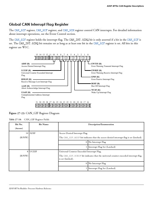
15 14 13 12 11 10 9 8 7 6 5 4 3 2 1 0 0000000000000000
ADIF (R) Access Denied Interrupt Flag
UCEIF (R) Universal Counter Exceeded Interrupt Flag
RMLIF (R) Receive Message Lost Interrupt Flag
ADSP-BF70x CAN Register Descriptions
Global CAN Interrupt Flag Register
The CAN_GIF register, CAN_GIF register, and CAN_GIM register control CAN interrupts. For detailed information about interrupt operations, see the Event Control section.
FPGA可编程逻辑器件芯片EP4CE55F23C8LN中文规格书
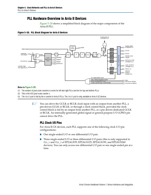
PLLs in Arria II Devices PLL Hardware Overview in Arria II DevicesFigure 5–20 shows a simplified block diagram of the major components of theArria II PLL.1You can drive the GCLK or RCLK clock input with an output from another PLL, apin-driven GCLK or RCLK, or through a clock control block, provided the clockcontrol block is fed by an output from another PLL, or a pin driven dedicated GCLK or RCLK. An internally-generated global signal or general purpose I/O (GPIO) pin cannot drive the PLL.PLL Clock I/O PinsFor Arria II GX devices, each PLL supports one of the following clock I/O pinconfigurations:■One single-ended I/O or one differential I/O pair.■Three single-ended I/O or three differential I/O pairs (this is only supported inPLL _1 and PLL _3 of EP2AGX95, EP2AGX125, EP2AGX190, and EP2AGX260devices). You can only access one differential I/O pair or one single-ended pin at a time.Figure 5–20.PLL Block Diagram for Arria II DevicesNotes to Figure 5–20:(1)The number of post-scale counters is seven for left and right PLLs and ten for top and bottom PLLs.(2)This is the VCO post-scale counter K .(3)The FBOUT port is fed by the M counter in Arria II PLLs. The FBOUT port is only available in Arria II GZ devices.Table5–11.RCLK Outputs From the PLL Clock Outputs for Arria II GZ Device(Part 2 of 2)PLL NumberClock ResourceL2L3B1B2R2R3T1T2 RCLK[32..43]————v v——RCLK[44..63]——————v vClock Control BlockEvery GCLK and RCLK network has its own clock control block. The control blockprovides the following features:■Clock source selection (dynamic selection for GCLKs)■GCLK multiplexing■Clock power down (static or dynamic clock enable or disable)Figure5–12 shows the GCLK select blocks for Arria II devices.Figure5–12.GCLK Control Block for Arria II DevicesNotes to Figure5–12:(1)You can only dynamically control these clock select signals through internal logic when the device is operating in usermode.(2)These clock select signals can only be set through a configuration file (.sof or .pof) and cannot be dynamicallycontrolled during user mode operation.(3)The left side of the Arria II GX device only allows PLL counter outputs as the dynamic clock source selection to theGCLK network.(4)This is only available on the left side of the Arria II GX device.Select the clock source for the GCLK control block either statically with a setting in theQuartus II software or dynamically with an internal logic to drive the multiplexerselect inputs. When selecting the clock source dynamically, you can either select twoPLL outputs (such as C0 or C1), or a combination of clock pins or PLL outputs.Figure5–6.PCLK Networks in (EP2AGX95 and EP2AGX125 Devices)Figure5–7.PCLK Networks in (EP2AGX190 and EP2AGX260 Devices)。
FPGA可编程逻辑器件芯片XC7Z020-1CLG484I中文规格书

FPGA可编程逻辑器件芯⽚XC7Z020-1CLG484I中⽂规格书IntroductionThe Zynq?-7000 SoCs are available in -3, -2, -1, and -1LI speed grades, with -3 having the highest performance. The -1LI devices can operate at either of two programmable logic (PL) V CCINT/V CCBRAM voltages, 0.95V and 1.0V, and are screened for lower maximum static power. The speed specification of a -1LI device is the same as the -1 speed grade. When operated at PL V CCINT/V CCBRAM = 0.95V, the -1LI static and dynamic power is reduced. Zynq-7000 device DC and AC characteristics are specified in commercial, extended, industrial and expanded (Q-temp) temperature ranges. Except for the operating temperature range or unless otherwise noted, all the DC and AC electrical parameters are the same for a particular speed grade (that is, the timing characteristics of a -1 speed grade industrial device are the same as for a -1 speed grade commercial device). However, only selected speed grades and/or devices are available in the commercial, extended, industrial, or Q-temp temperature ranges.All supply voltage and junction temperature specifications are representative of worst-case conditions. The parameters included are common to popular designs and typical applications.The available device/package combinations are outlined in:?Zynq-7000SoC Overview (DS190)XA Zynq-7000SoC Overview (DS188)Defense-grade Zynq-7000Q SoC Overview (DS196)DC CharacteristicsZynq-7000SoC (Z-7007S, Z-7012S, Z-7014S, Z-7010, Z-7015, and Z-7020):DC and AC Switching CharacteristicsDS187 (v1.20.1) July 2, 2018Product SpecificationTable 1:Absolute Maximum Ratings(1)Symbol Description Min Max Units Processing System (PS)V CCPINT PS internal logic supply voltage–0.5 1.1VV CCPAUX PS auxiliary supply voltage–0.5 2.0VV CCPLL PS PLL supply–0.5 2.0VV CCO_DDR PS DDR I/O supply voltage–0.5 2.0VV CCO_MIO(2)PS MIO I/O supply voltage–0.5 3.6VV PREF PS input reference voltage–0.5 2.0VV PIN(2)(3)(4)(5)PS MIO I/O input voltage–0.40V CCO_MIO+0.55V PS DDR I/O input voltage–0.55V CCO_DDR+0.55V Programmable Logic (PL)V CCINT PL internal supply voltage–0.5 1.1V V CCAUX PL auxiliary supply voltage–0.5 2.0V V CCBRAM PL supply voltage for the block RAM memories–0.5 1.1V V CCO PL supply voltage for HR I/O banks–0.5 3.6V V REF Input reference voltage–0.5 2.0VPL I/O LevelsTable 10:SelectIO DC Input and Output Levels(1)(2)I/O StandardV IL V IH V OL V OH I OL I OH V, Min V, Max V, Min V, Max V, Max V, Min mA mAHSTL_I–0.300V REF–0.100V REF+0.100V CCO+0.3000.400V CCO–0.4008.00–8.00 HSTL_I_18–0.300V REF–0.100V REF+0.100V CCO+0.3000.400V CCO–0.4008.00–8.00 HSTL_II–0.300V REF–0.100V REF+0.100V CCO+0.3000.400V CCO–0.40016.00–16.00 HSTL_II_18–0.300V REF–0.100V REF+0.100V CCO+0.3000.400V CCO–0.40016.00–16.00 HSUL_12–0.300V REF–0.130VREF+0.130V CCO+0.30020%V CCO80%V CCO0.10–0.10 LVCMOS12–0.30035% V CCO65% V CCO V CCO+0.3000.400V CCO–0.400Note3Note3 LVCMOS15–0.30035% V CCO65% V CCO V CCO+0.30025%V CCO75%V CCO Note4Note4 LVCMOS18–0.30035% V CCO65% V CCO V CCO+0.3000.450V CCO–0.450Note5Note5 LVCMOS25–0.3000.7 1.700V CCO+0.3000.400V CCO–0.400Note4Note4 LVCMOS33–0.3000.8 2.000 3.4500.400V CCO–0.400Note4Note4 LVTTL–0.3000.8 2.000 3.4500.4002.400Note5Note5 MOBILE_DDR–0.30020% V CCO80% V CCO V CCO+0.30010%V CCO90%V CCO0.10–0.10 PCI33_3–0.40030% V CCO50% V CCO V CCO+0.50010%V CCO90%V CCO 1.50–0.50 SSTL135–0.300V REF–0.090V REF+0.090V CCO+0.300V CCO/2–0.150V CCO/2+0.15013.00–13.00 SSTL135_R–0.300V REF–0.090V REF+0.090V CCO+0.300V CCO/2–0.150V CCO/2+0.1508.90–8.90 SSTL15–0.300V REF–0.100V REF+0.100V CCO+0.300V CCO/2–0.175V CCO/2+0.17513.00–13.00 SSTL15_R–0.300V REF–0.100V REF+0.100V CCO+0.300V CCO/2–0.175V CCO/2+0.1758.90–8.90 SSTL18_I–0.300V REF–0.125V REF+0.125V CCO+0.300VCCO/2–0.470V CCO/2+0.4708.00–8.00 SSTL18_II–0.300V REF–0.125V REF+0.125V CCO+0.300V CCO/2–0.600VCCO/2+0.60013.40–13.40 Notes:1.Tested according to relevant specifications.2. 3.3V and 2.5V standards are only supported in HR I/O banks.3.Supported drive strengths of 4, 8, or 12mA in HR I/O banks.4.Supported drive strengths of 4, 8, 12, or 16mA in HR I/O banks.5.Supported drive strengths of 4, 8, 12, 16, or 24mA in HR I/O banks.6.For detailed interface specific DC voltage levels, see the 7Series FPGAs SelectIO Resources User Guide (UG471).Table 11:Differential SelectIO DC Input and Output LevelsI/O StandardV ICM(1)V ID(2)V OCM(3)V OD(4)V, Min V, Typ V, Max V, Min V, Typ V, Max V, Min V, Typ V, Max V, Min V, T yp V, MaxBLVDS_250.300 1.200 1.4250.100––– 1.250 –Note5MINI_LVDS_250.300 1.200V CCAUX0.2000.4000.600 1.000 1.200 1.4000.3000.4500.600 PPDS_250.2000.900VCCAUX0.1000.2500.4000.5000.950 1.4000.1000.2500.400 RSDS_250.3000.900 1.5000.1000.3500.600 1.000 1.2001.4000.1000.3500.600 TMDS_332.700 2.9653.2300.1500.675 1.200V CCO–0.405V CCO–0.300V CCO–0.1900.4000.6000.800 Notes:1.V ICM is the input common mode voltage.2.V ID is the input differential voltage (Q–Q).3.V OCM is the output common mode voltage.4.V OD is the output differential voltage (Q–Q).5.V OD for BLVDS will vary significantly depending on topology and loading.6.LVDS_25 is specified in Table13.Figure 2:DDR Output Timing Diagram。
FPGA可编程逻辑器件芯片EP4CE55F23A7N中文规格书

Differential Pin Placement GuidelinesUsing Both Center PLLsYou can use center PLLs to drive DPA-enabled channels simultaneously, if they drivethese channels in their adjacent banks only, as shown in Figure8–23.1Center PLLs are available at the right I/O banks of Arria II GX devices and the right and left I/O banks of Arria II GZ devices.If one of the center PLLs drives the DPA-enabled channels in the upper and lower I/Obanks, you cannot use the other center PLL for DPA-enabled channels, as shown inFigure8–24.Figure8–24.Center PLLs Driving DPA-Enabled Differential I/OsDocument Revision History July 2010 3.0Updated for Arria II GX v10.0 release:■Updated Table 8–1 and Table 8–2.■Updated Figure 8–1 and Figure 8–5.■Updated “Non-DPA Mode” section.■Removed Table 8–1: Supported Data Range.■Minor text edit.November 2009 2.0Updated for Arria II GX v9.1 release:■Updated Table 8–1 and Table 8–2.■Updated Figure 8–1.■Updated “LVDS Channels” and “Non-DPA Mode” sections.■Minor text edit.June 20091.1■Updated Table 8–2 and Table 8–3.■Updated “Programmable Pre-Emphasis and Programmable VOD.” and “LVDS Channels”sections.February 2009 1.0Initial release Table 8–9.Document Revision History (Part 2 of 2)Date VersionChanges MadePower-On Reset Circuit and Configuration Pins Power Supply Configuration Pins Power SupplyTable 9–4 lists the configuration pins for Arria II devices.Arria II devices do not support a 1.5-V configuration. The operating voltage for the configuration input pin is independent of the I/O banks power supply V CCIO during configuration. Therefore, for Arria II devices, you do not require configuration voltage constraints on V CCIO .f For more information, refer to the Power Management in Arria II Devices chapter.f For more information about the configuration pins connection recommendations,refer to the Arria II Device Family Pin Connection Guidelines .Table 9–4.Configuration pins for Arria II Devices Devices Configuration PinsArria II GX All dedicated configuration pins are supplied by V CCIO for I/O banks 3C and 8C inwhich they reside. The supported configuration voltages are 1.8, 2.5, 3.0, and3.3V. Use the V CCIO pin for I/O banks 3C and 8C to power all the dedicatedconfiguration inputs, dedicated configuration outputs, and dedicatedconfiguration bidirectional pins that you used for configuration. With V CCIO forI/O banks 3C and 8C, the configuration input buffers do not have to the sharepower lines with the regular I/O buffer.You must power the dual function configuration pins that you used forconfiguration with the V CCIO power supply in which the configuration pins reside.For more information about the configuration voltage standard applied to theV CCIO power supply, refer to Table 9–6 on page 9–9.Arria II GZAll dedicated configuration pins and dual-function pins are supplied by V CCPGM .The supported configuration voltages are 1.8, 2.5, and 3.0V. Use the V CCPGM pinto power all the dedicated configuration inputs, dedicated configuration outputs,and dedicated configuration bidirectional pins that you used for configuration.With V CCPGM , the configuration input buffers do not have to share the power lineswith the regular I/O buffer.。
FPGA可编程逻辑器件芯片EP4CGX75CF23C7中文规格书

Chapter 7:External Memory Interfaces in Arria II DevicesMemory Interfaces Pin Support for Arria II Devices The numbering scheme starts from the top-left corner of the device goingcounter-clockwise in a die top view. Figure7–17 shows how the DQ/DQS groups arenumbered in a die top view of the device.Figure7–17.DQS Pins in Arria II GZ I/O BanksFigure7–9 shows the number of DQ/DQS groups per bank in Arria II GX EP2AGX95and EP2AGX125 devices in the 1152-pin FineLine BGA package.Figure7–9.Number of DQ/DQS Groups per Bank in EP2AGX95 and EP2AGX125 Devices in the 1152-Pin FineLine BGA Package (Note1)Notes to Figure7–9:(1)All I/O pin counts include 12 dedicated clock inputs (CLK4 to CLK15) that you can use for data inputs.(2)Several configuration pins in Bank 6A are shared with DQ/DQS pins. You cannot use a 4 DQ/DQS group with any of their pin members used forconfiguration purposes. Ensure that the DQ/DQS groups you chose are not also used for configuration.Figure7–13 shows the number of DQ/DQS groups per bank in Arria II GZEP2AGZ300 and EP2AGZ350 devices in the 1152-pin FineLine BGA package.Figure7–13.Number of DQ/DQS Groups per Bank in EP2AGZ300 and EP2AGZ350 Devices in the 1152-Pin FineLine BGA Package(Note1), (2), (3)Notes to Figure7–13:(1)You can also use DQS/DQSn pins in some of the ×4 groups as R UP and R DN pins, but you cannot use a ×4 group for memory interfaces if two pinsof the ×4 group are used as R UP and R DN pins for OCT calibration. If two pins of a ×4 group are used as R UP and R DN pins for OCT calibration, you can use the ×16/×18 or ×32/×36 groups that include that ×4 group; however, there are restrictions on using ×8/×9 groups that include that ×4 group.(2)All I/O pin counts include dedicated clock inputs that you can use for data inputs.(3)You can also use some of the DQ/DQS pins in I/O Bank 1C as configuration pins. You cannot use a ×4 DQ/DQS group with any of its pin membersused for configuration purposes. Ensure that the DQ/DQS groups that you have chosen are not also used for configuration because you may lose up to four ×4 DQ/DQS groups, depending on your configuration scheme.(4)These ×32/×36 DQ/DQS groups have 40 pins instead of 48 pins per group.。
FPGA可编程逻辑器件芯片EP4CGX75CF23C8N中文规格书

Chapter 4:DSP Blocks in Arria II DevicesArria II Operational Mode Descriptions36-Bit MultiplierYou can construct a 36×36 multiplier with four 18×18 multipliers. Thissimplification fits into one half-DSP block and is implemented in the DSP blockautomatically by selecting 36×36 mode. Arria II devices can have up to two 36-bitmultipliers per DSP block (one 36-bit multiplier per half DSP block). The 36-bitmultiplier is also under the independent multiplier mode but uses the entire half-DSPblock, including the dedicated hardware logic after the pipeline registers toimplement the 36×36-bit multiplication operation, as shown in Figure4–10.The 36-bit multiplier is useful for applications requiring more than 18-bit precision;for example, for the mantissa multiplication portion of single precision and extendedsingle precision floating-point arithmetic applications.Figure4–10.36-Bit Independent Multiplier Mode Shown for Half-DSP BlockDouble MultiplierYou can configure the Arria II DSP block to support an unsigned 54×54-bit multiplierthat is required to compute the mantissa portion of an IEEE double precision floatingpoint multiplication. You can build a 54×54-bit multiplier with basic 18×18multipliers, shifters, and adders. To efficiently use built-in shifters and adders in theArria II DSP block, a special double mode (partial 54×54 multiplier) is available thatChapter 2:Logic Array Blocks and Adaptive Logic Modules in Arria II DevicesAdaptive Logic ModulesThis feature is called register packing. It improves device utilization by allowing thedevice to use the register and combinational logic for unrelated functions. Anothermechanism to improve fitting is to allow the register output to feed back into the LUTof the same ALM so that the register is packed with its own fan-out LUT. The ALMcan also drive out registered and unregistered versions of the LUT or adder output.The Quartus II software automatically configures the ALMs for optimizedperformance.ALM Operating ModesThe Arria II ALM can operate in any of the following modes:■Normal■Extended LUT■Arithmetic■Shared Arithmetic■LUT-RegisterThe Quartus II software and other supported third-party synthesis tools, inconjunction with parameterized functions such as the library of parameterizedmodules (LPM) functions, automatically choose the appropriate mode for commonfunctions such as counters, adders, subtractors, and arithmetic functions. Each modeuses the ALM resources differently. In each mode, eleven available inputs to anALM—the eight data inputs from the LAB local interconnect, carry-in from theprevious ALM or LAB, the shared arithmetic chain connection from the previousALM or LAB, and the register chain connection—are directed to different destinationsto implement the desired logic function. LAB-wide signals provide clock,asynchronous clear, synchronous clear, synchronous load, and clock enable control forthe register. These LAB-wide signals are available in all ALM modes. For moreinformation on the LAB-wide control signals, refer to “LAB Control Signals” onpage2–4.Chapter 5:Clock Networks and PLLs in Arria II DevicesClock Networks in Arria II Devicesf For more information, refer to the Clock Control Block (ALTCLKCTRL) MegafunctionUser Guide.Figure5–13 and Figure5–14 show the RCLK select blocks.Figure5–13.RCLK Control Block for Arria II GX DevicesNote to Figure5–13:(1)This clock select signal can only be statically controlled through a configuration file (.sof or .pof) and cannot bedynamically controlled during user mode operation.Figure5–14.RCLK Control Block for Arria II GZ DevicesNotes to Figure5–14:(1)When the device is in user mode, you can only set the clock select signals through a configuration file(.sof or .pof). You cannot dynamically control the clock.(2)The CLKn pin is not a dedicated clock input when used as a single-ended PLL clock input.。
FPGA可编程逻辑器件芯片XC7Z100-2FF900I中文规格书

I/O Standard Adjustment Measurement Methodology Input Delay MeasurementsTable58 shows the test setup parameters used for measuring input delay. Table 58:Input Delay Measurement MethodologyDescription I/O Standard Attribute V L(1)(2)V H(1)(2)V MEAS(1)(4)(6)V REF(1)(3)(5)LVCMOS, 1.2V LVCMOS120.1 1.10.6–LVCMOS, 1.5V LVCMOS150.1 1.40.75–LVCMOS, 1.8V LVCMOS180.1 1.70.9–LVCMOS, 2.5V LVCMOS250.1 2.4 1.25–LVCMOS, 3.3V LVCMOS330.1 3.2 1.65–LVTTL, 3.3V LVTTL0.1 3.2 1.65–MOBILE_DDR, 1.8V MOBILE_DDR0.1 1.70.9–PCI33, 3.3V PCI33_30.1 3.2 1.65–HSTL (High-Speed Transceiver Logic), Class I, 1.2V HSTL_I_12V REF–0.5V REF+0.5V REF0.60 HSTL, Class I & II, 1.5V HSTL_I, HSTL_II V REF–0.65V REF+0.65V REF0.75 HSTL, Class I & II, 1.8V HSTL_I_18, HSTL_II_18V REF–0.8V REF+0.8V REF0.90 HSUL (High-Speed Unterminated Logic), 1.2V HSUL_12V REF–0.5V REF+0.5V REF0.60 SSTL (Stub Terminated Transceiver Logic), 1.2V SSTL12V REF–0.5V REF+0.5V REF0.60 SSTL, 1.35V SSTL135, SSTL135_R V REF–0.575V REF+0.575V REF0.675 SSTL, 1.5V SSTL15, SSTL15_R V REF–0.65V REF+0.65V REF0.75 SSTL, Class I & II, 1.8V SSTL18_I, SSTL18_II V REF–0.8V REF+0.8V REF0.90 DIFF_MOBILE_DDR, 1.8V DIFF_MOBILE_DDR0.9–0.1250.9+0.1250(6)–DIFF_HSTL, Class I, 1.2V DIFF_HSTL_I_120.6–0.1250.6+0.1250(6)–DIFF_HSTL, Class I & II,1.5V DIFF_HSTL_I,DIFF_HSTL_II0.75–0.1250.75+0.1250(6)–DIFF_HSTL, Class I & II, 1.8V DIFF_HSTL_I_18,DIFF_HSTL_II_180.9–0.1250.9+0.1250(6)–DIFF_HSUL, 1.2V DIFF_HSUL_120.6–0.1250.6+0.1250(6)–DIFF_SSTL, 1.2V DIFF_SSTL120.6–0.1250.6+0.1250(6)–DIFF_SSTL135/DIFF_SSTL135_R, 1.35V DIFF_SSTL135,DIFF_SSTL135_R0.675–0.1250.675+0.1250(6)–DIFF_SSTL15/DIFF_SSTL15_R, 1.5V DIFF_SSTL15,DIFF_SSTL15_R0.75–0.1250.75+0.1250(6)–DIFF_SSTL18_I/DIFF_SSTL18_II, 1.8V DIFF_SSTL18_I,DIFF_SSTL18_II0.9–0.1250.9+0.1250(6)–LVDS (Low-Voltage Differential Signaling), 1.8V LVDS0.9–0.1250.9+0.1250(6)–LVDS_25, 2.5V LVDS_25 1.2–0.125 1.2+0.1250(6)–BLVDS_25, 2.5V BLVDS_25 1.25–0.125 1.25+0.1250(6)–MINI_LVDS_25, 2.5V MINI_LVDS_25 1.25–0.125 1.25+0.1250(6)–PPDS_25PPDS_25 1.25–0.125 1.25+0.1250(6)–RSDS_25RSDS_25 1.25–0.125 1.25+0.1250(6)–质量等级领域:宇航级IC、特军级IC、超军级IC、普军级IC、禁运IC、工业级IC,军级二三极管,功率管等;应用领域:航空航天、船舶、汽车电子、军用计算机、铁路、医疗电子、通信网络、电力工业以及大型工业设备祝您:工作顺利,生活愉快!以赛灵思半导体(深圳)有限公司提供的参数为例,以下为XC7Z100-2FF900I的详细参数,仅供参考Generator (FF and RF Packages)(1)(2)Memory Standard I/O Bank Type V CCAUX_IOSpeed GradeUnits-3E-2E/-2I-2LI-1C/-1I-1Q/-1LQ4:1 Memory ControllersDDR3HP 2.0V1866(3)1866(3)160016001066Mb/s HP 1.8V1600133313331066800Mb/s HR N/A106610661066800800Mb/sDDR3L HP 2.0V16001600160013331066Mb/s HP 1.8V133310661066800800Mb/s HR N/A800800800667N/A Mb/sDDR2HP 2.0V800800800800667Mb/s HP 1.8V800800800800667Mb/s HR N/A800800800800533Mb/sRLDRAM III HP 2.0V800667667667550MHz HP 1.8V550500500450400MHz HR N/A N/A2:1 Memory ControllersDDR3HP 2.0V106610661066800667Mb/s HP 1.8V Mb/s HR N/A Mb/sDDR3L HP 2.0V106610661066800667Mb/s HP 1.8V Mb/s HR N/A800800800667N/A Mb/sDDR2HP 2.0V800800800800667Mb/s HP 1.8V667HR N/A533QDR II+(4)HP 2.0V550500500450300MHz HP 1.8VHR N/A500450450400300MHzRLDRAM II HP 2.0V533500500450400MHz HP 1.8VHR N/ALPDDR2HP 2.0V667667667667533Mb/s HP 1.8V Mb/s HR N/A Mb/sNotes:1.V REF tracking is required. For more information, see the Zynq-7000 SoC and 7Series Devices Memory Interface Solutions UserGuide(UG586).2.When using the internal V REF, the maximum data rate is 800Mb/s (400MHz).3.For designs using 1866Mb/s components, contact Xilinx Technical Support.4.The maximum QDRII+ performance specifications are for burst-length 4 (BL=4) implementations. Burst length 2 (BL=2) implementationsare limited to 333MHz for all speed grades and I/O bank types.Generator (FB, RB, and SB Packages)(1)(2)。
FPGA可编程逻辑器件芯片EP4CE40F23C7N中文规格书

Arria II Device Handbook Volume 1: Device Interfaces and Integration July 2012 1.Overview for the Arria II Device FamilyThe Arria ® II device family is designed specifically for ease-of-use. The cost-optimized, 40-nm device family architecture features a low-power, programmable logic engine and streamlined transceivers and I/Os. Common interfaces, such as the Physical Interface for PCI Express ® (PCIe ®), Ethernet, and DDR3 memory are easily implemented in your design with the Quartus ®II software, the SOPC Builder design software, and a broad library of hard and soft intellectual property (IP) solutions from Altera. The Arria II device family makes designing for applications requiring transceivers operating at up to 6.375Gbps fast and easy.This chapter contains the following sections:■“Arria II Device Feature” on page 1–1■“Arria II Device Architecture” on page 1–6■“Reference and Ordering Information” on page 1–14Arria II Device FeatureThe Arria II device features consist of the following highlights:■40-nm, low-power FPGA engine■Adaptive logic module (ALM) offers the highest logic efficiency in the industry ■Eight-input fracturable look-up table (LUT)■Memory logic array blocks (MLABs) for efficient implementation of small FIFOs■High-performance digital signal processing (DSP) blocks up to 550MHz ■Configurable as 9 x 9-bit, 12 x 12-bit, 18 x 18-bit, and 36 x 36-bit full-precision multipliers as well as 18 x 36-bit high-precision multiplier■Hardcoded adders, subtractors, accumulators, and summation functions ■Fully-integrated design flow with the MATLAB and DSP Builder software from Altera ■Maximum system bandwidth■Up to 24 full-duplex clock data recovery (CDR)-based transceivers supporting rates between 600Mbps and 6.375Gbps■Dedicated circuitry to support physical layer functionality for popular serial protocols, including PCIe Gen1 and PCIe Gen2, Gbps Ethernet, Serial RapidIO ® (SRIO), Common Public Radio Interface (CPRI), OBSAI,SD/HD/3G/ASI Serial Digital Interface (SDI), XAUI and Reduced XAUI (RXAUI), HiGig/HiGig+, SATA/Serial Attached SCSI (SAS), GPON,SerialLite II, Fiber Channel, SONET/SDH, Interlaken, Serial Data Converter (JESD204), and SFI-5.Chapter 2:Logic Array Blocks and Adaptive Logic Modules in Arria II DevicesAdaptive Logic Modules Arria II Device Handbook Volume 1: Device Interfaces and Integration ALM InterconnectsThere are three dedicated paths between ALMs: Register Cascade, Carry-chain, and Shared Arithmetic chain. Arria II devices include an enhanced interconnect structure in LABs for routing shared arithmetic chains and carry chains for efficient arithmetic functions. The register chain connection allows the register output of one ALM to connect directly to the register input of the next ALM in the LAB for fast shiftregisters. These ALM-to-ALM connections bypass the local interconnect. Figure 2–15 shows the shared arithmetic chain, carry chain, and register chain interconnects.Clear and Preset Logic ControlLAB-wide signals control the logic for the register‘s clear signal. The ALM directly supports an asynchronous clear function. You can achieve the register preset through the Quartus II software’s NOT-gate push-back logic option. Each LAB supports up to two clears. Arria II devices provide a device-wide reset pin (DEV_CLRn ) that resets all registers in the device. An option set before compilation in the Quartus II software enables this pin. This device-wide reset overrides all other control B Power Management TechniquesThe following techniques are used to manage static and dynamic power consumption within the LAB:■The Quartus II software forces all adder inputs low when ALM adders are not in use to save AC power.■Arria II LABs operate in high-performance mode or low-power mode. TheQuartus II software automatically chooses the appropriate mode for the LAB,based on the design, to optimize speed versus leakage trade-offs.Figure 2–15.Shared Arithmetic Chain, Carry Chain, and Register Chain InterconnectsCarry chain & sharedarithmetic chainro u ting to adjacent ALM Localinterconnect Register chain ro u ting to adjacent ALM's register inp u t Local interconnectro u ting among ALMs....Chapter 2:Logic Array Blocks and Adaptive Logic Modules in Arria II DevicesAdaptive Logic Modules Arria II Device Handbook Volume 1: Device Interfaces and Integration Arithmetic ModeArithmetic mode is ideal for implementing adders, counters, accumulators, wideparity functions, and comparators. The ALM in arithmetic mode uses two sets of two 4-input LUTs along with two dedicated full adders. The dedicated adders allow the LUTs to be available to perform pre-adder logic; therefore, each adder can add the output of two 4-input functions. The four LUTs share dataa and datab inputs. As shown in Figure 2–10, the carry-in signal feeds to adder0 and the carry-out fromadder0 feeds to the carry-in of adder1. The carry-out from adder1 drives to adder0 of the next ALM in the LAB. ALMs in arithmetic mode can drive out registered and unregistered versions of the adder outputs.In arithmetic mode, the ALM supports simultaneous use of the adder’s carry output along with combinational logic outputs. The adder output is ignored in this operation. Using the adder with combinational logic output provides resource savings of up to 50% for functions that can use this mode.Arithmetic mode also offers clock enable, counter enable, synchronous up and down control, add and subtract control, synchronous clear, and synchronous load. The LAB local interconnect data inputs generate the clock enable, counter enable, synchronous up and down, and add and subtract control signals. These control signals are good candidates for the inputs that share the four LUTs in the ALM. The synchronous clear and synchronous load options are LAB-wide signals that affect all registers in the LAB. These signals can also be individually disabled or enabled per register. TheQuartus II software automatically places any registers that are not used by the counter into other LABs.Figure 2–10.ALM in Arithmetic Modedatae0carry_incarry_o u t dataa data bdatacdatadTo general orlocal ro u ting To general orlocal ro u tingTo general or local ro u ting To general or local ro u tingdataf0dataf1。
FPGA可编程逻辑器件芯片EP4CE55F23I7N中文规格书

1Altera recommends performing IBIS or SPICE simulations to determine the rightcurrent strength setting for your specific application.HSTL-12 Class I12, 10, 8HSTL-12 Class II16BLVDS8, 12, 16Notes to Table 6–7:(1)The default current strength setting in the Quartus II software is 50-Ω R S OCT without calibration for allnon-voltage reference and HSTL/SSTL Class I I/O standards. The default setting is 25-Ω R S OCT without calibrationfor HSTL/SSTL Class II I/O standards.(2)The default current strength setting in the Quartus II software is the current strength shown in brackets [].Table 6–8.Programmable Current Strength for Arria II GZ Devices (Note 1), (2)I/O StandardI OH / I OL Current Strength Setting (mA) for Column I/O Pins I OH / I OL Current Strength Setting (mA) for Row I/O Pins 3.3-V LVTTL16, 12, 8, 412, 8, 43.3-V LVCMOS16, 12, 8, 48, 42.5-V LVCMOS16, 12, 8, 412, 8, 41.8-V LVCMOS12, 10, 8, 6, 4, 28, 6, 4, 21.5-V LVCMOS12, 10, 8, 6, 4, 28, 6, 4, 21.2-V LVCMOS8, 6, 4, 24, 2SSTL-2 Class I12, 10, 812, 8SSTL-2 Class II1616SSTL-18 Class I12, 10, 8, 6, 412, 10, 8, 6, 4SSTL-18 Class II16, 816, 8SSTL-15 Class I12, 10, 8, 6, 48, 6, 4SSTL-15 Class II16, 8—HSTL-18 Class I12, 10, 8, 6, 412, 10, 8, 6, 4HSTL-18 Class II1616HSTL-15 Class I12, 10, 8, 6, 48, 6, 4HSTL-15 Class II16—HSTL-12 Class I12, 10, 8, 6, 48, 6, 4HSTL-12 Class II16—Notes to Table 6–8:(1)The default setting in the Quartus II software is 50-Ω R S OCT without calibration for all non-voltage reference andHSTL and SSTL Class I I/O standards. The default setting is 25-Ω R S OCT without calibration for HSTL and SSTLClass II I/O standards.(2)The 3.3-V LVTTL and 3.3-V LVCMOS are supported using V CCIO and V CCPD at 3.0 V.Table 6–7.Programmable Current Strength for Arria II GX Devices (Note 1)(Part 2 of 2)I/O StandardI OL / I OH Current Strength Setting (mA) for Top, Bottom, and Right I/O PinsModular I/O BanksThe I/O pins in Arria II devices are arranged in groups called modular I/O banks.Depending on the device densities, the number of I/O banks range from 6 to 20.Table6–3 and Table6–4 show the number of I/O pins available in each I/O bank. Table6–3.Available I/O Pins in Each Arria II GX I/O Bank (Note1)Package DeviceBankTotal 3A3B4A4B5A5B6A6B7A7B8A8B358-pin Flip Chip UBGA EP2AGX4522—38—18—18—38—22—156 EP2AGX6522—38—18—18—38—22—156572-pin Flip Chip FBGA EP2AGX4538—38—50—50—38—38—252 EP2AGX6538—38—50—50—38—38—252 EP2AGX9538—42—50—50—38—42—260 EP2AGX12538—42—50—50—38—42—260780-pin Flip Chip FBGA EP2AGX4554—70—66—50—70—54—364 EP24GX6554—70—66—50—70—54—364 EP2AGX9554—74—66—50—70—58—372 EP2AGX12554—74—66—50—70—58—372 EP2AGX19054—74—66—50—70—58—372 EP2AGX26054—74—66—50—70—58—3721152-pin Flip Chip FBGA EP2AGX9570—741666—66—701674—452 EP2AGX12570—741666—66—701674—452 EP2AGX190703274326632663270327432612 EP2AGX260703274326632663270327432612Note to Table6–3:(1)The number of I/O pins include all general purpose I/Os, dedicated clock pins, and dual-purpose configuration pins. Transceiver pins and dedicatedconfiguration pins are not included in the I/O pin count.Devices This section provides information on Arria® II device I/O features, external memoryinterfaces, and high-speed differential interfaces with DPA. This section includes thefollowing chapters:■Chapter6, I/O Features in Arria II Devices■Chapter7, External Memory Interfaces in Arria II Devices■Chapter8, High-Speed Differential I/O Interfaces and DPA in Arria II DevicesRevision HistoryRefer to each chapter for its own specific revision history. For information on wheneach chapter was updated, refer to the Chapter Revision Dates section, which appearsin this volume.。
FPGA可编程逻辑器件芯片XC7K325T-2FFG900I中文规格书

FPGA可编程逻辑器件芯⽚XC7K325T-2FFG900I中⽂规格书Chapter1 Packaging OverviewAbout this GuideXilinx? 7series FPGAs include four FPGA families that are all designed for lowest power to enable a common design to scale across families for optimal power, performance, and cost.The Spartan?-7 family is the lowest density with the lowest cost entry point into the7series portfolio. The Artix?-7 family is optimized for highest performance-per-watt and bandwidth-per-watt for cost-sensitive, high-volume applications. The Kintex?-7 family is an innovative class of FPGAs optimized for the best price-performance. The Virtex?-7family is optimized for highest system performance and capacity.This 7series packaging and pinout product specification, part of an overall set ofdocumentation on the 7series FPGAs, is available on the Xilinx website .IntroductionThis section describes the pinouts for the 7series FPGAs in various fine pitch and flip-chip1.0mm pitch BGA packages, 0.8mm and 0.5mm pitch chip-scale packages, and 0.5mmpitch wire-bond lead frame packages.Spartan-7, Artix-7, and Kintex-7 devices are offered in low-cost, space-saving packages that are optimally designed for the maximum number of user I/Os.Virtex-7T and Virtex-7XT devices are offered exclusively in high performance flip-chip BGA packages that are optimally designed for improved signal integrity and jitter.For pinout and packaging information on the Virtex-7HT devices.Package inductance is minimized as a result of optimal placement and even distributionas well as an increased number of Power and GND pins.The FFG, FLG, FHG, FBG, SBG, and RFG flip-chip packages marked with the Pb-free Character on the upper right of the device are RoHS 6 of 6 compliant. The FFG, FLG, FHG, FBG, SBG, and RFG flip-chip packages not marked with the Pb-free character are RoHS 6 of 6 compliant,Pin DefinitionsTable1-12 lists the pin definitions used in 7series FPGAs packages.Note:There are dedicated general purpose user I/O pins listed separately in Table1-12. There are also multi-function pins where the pin names start with either IO_LXXY_ZZZ_# or IO_XX_ZZZ_#, where ZZZ represents one or more functions in addition to being general purpose user I/O. If not used for their special function, these pins can be user I/O.user I/O after stage 2 configuration is complete.Power/Ground PinsGND Dedicated N/A GroundRSVDGND Dedicated N/A Reserved pins, tie to GNDVCCAUX Dedicated N/A 1.8V power-supply pins for auxiliary circuits VCCAUX_IO_G#(2)Dedicated N/A 1.8V/2.0V power-supply pins for auxiliary I/O circuits VCCINT Dedicated N/A0.9V/1.0V power-supply pins for the internal core logic VCCO_# (3)Dedicated N/A Power-supply pins for the output drivers (per bank) VCCBRAM Dedicated N/A 1.0V power-supply pins for the FPGA logic block RAMVCCBATT_0Dedicated N/A Decryptor key memory backup supply; this pin should be tied to the appropriate V CC or GND when not used(4). Specific Spartan-7 devices (XC7S6 and XC7S15) do not support AES encryption. In these devices, connect VCCBATT_0 to VCCAUX or GND.VREF Multi-function N/A These are input threshold voltage pins. They become user I/Os when an external threshold voltage is not needed (per bank).Analog to Digital Converter (XADC) PinsFor more information, see the XADC Package Pins table in UG480, 7Series FPGAs and Zynq-7000 All Programmable SoC XADC Dual 12-Bit 1 MSPS Analog-to-Digital Converter User GuideVCCADC_0(5)(6)Dedicated N/A XADC analog positive supply voltageThe XC7S6 and XC7S15 Spartan-7 devices do not support the XADC. In these devices, connect the VCCADC_0 pin to VCCAUX.GNDADC_0(5)(6)Dedicated N/A XADC analog ground referenceThe XC7S6 and XC7S15 Spartan-7 devices do not support the XADC. In these devices, connect the GNDADC_0 pin to GND.VP_0(5)Dedicated Input XADC dedicated differential analog input (positive side) VN_0(5)Dedicated Input XADC dedicated differential analog input (negative side) VREFP_0(5)Dedicated N/A 1.25V reference inputVREFN_ 0(5)Dedicated N/A 1.25V reference GND referenceAD0P through AD15PAD0N through AD15N Multi-function Input XADC (analog-to-digital converter) differential auxiliary analog inputs 0–15. Auxiliary channels 6, 7, 13, 14, and 15 are not supported on Kintex-7 devices.Table 1-12:7Series FPGAs Pin Definitions (Cont’d)Pin Name Type Direction DescriptionChapter 2:7Series FPGAs Package Files。
FPGA可编程逻辑器件芯片XC7Z100-2FFG900I中文规格书

IntroductionThe Zynq®-7000 SoCs are available in -3, -2, -2LI, -1, and -1LQ speed grades, with -3 having the highest performance. The -2LI devices operate at programmable logic (PL)V CCINT/V CCBRAM=0.95V and are screened for lower maximum static power. The speed specification of a -2LI device is the same as that of a -2device. The -1LQ devices operate at the same voltage and speed as the -1Q devices and are screened for lower power. Zynq-7000 device DC and AC characteristics are specified in commercial, extended, industrial, and expanded (Q-temp) temperature ranges. Except the operating temperature range or unless otherwise noted, all the DC and AC electrical parameters are the same for a particular speed grade (that is, the timing characteristics of a -1 speed grade industrial device are the same as for a -1 speed grade commercial device). However, only selected speed grades and/or devices are available in the commercial, extended, or industrial temperature ranges.All supply voltage and junction temperature specifications are representative of worst-case conditions. The parameters included are common to popular designs and typical applications.The available device/package combinations are outlined in:•Zynq-7000SoC Overview (DS190)•Defense-grade Zynq-7000Q SoC Overview (DS196)•XA Zynq-7000SoC Overview (DS188)This Zynq-7000SoC data sheet, which covers the specifications for the XC7Z030, XA7Z030, XQ7Z030,XC7Z035, XC7Z045, XQ7Z045, XC7Z100, and XQ7Z100 complements the Zynq-7000SoC documentation suite available on the Xilinx website.DC CharacteristicsZynq-7000SoC (Z-7030, Z-7035, Z-7045, and Z-7100): DC and AC Switching CharacteristicsDS191 (v1.18.1) July 2, 2018Product SpecificationTable 1:Absolute Maximum Ratings(1)Symbol Description Min Max Units Processing System (PS)V CCPINT PS internal logic supply voltage–0.5 1.1VV CCPAUX PS auxiliary supply voltage–0.5 2.0VV CCPLL PS PLL supply–0.5 2.0VV CCO_DDR PS DDR I/O supply–0.5 2.0VV CCO_MIO(2)PS MIO I/O supply–0.5 3.6VV PREF PS input reference voltage–0.5 2.0VV PIN(2)(3)(4)(5)PS MIO I/O input voltage–0.40V CCO_MIO+0.55V PS DDR I/O input voltage–0.55V CCO_DDR+0.55V Programmable Logic (PL)V CCINT PL internal supply voltage–0.5 1.1VV CCBRAM PL supply voltage for the block RAM memories–0.5 1.1VV CCAUX PL auxiliary supply voltage–0.5 2.0VV CCO PL output drivers supply voltage for HR I/O banks–0.5 3.6V PL output drivers supply voltage for HP I/O banks–0.5 2.0VV CCAUX_IO(4)Auxiliary supply voltage–0.5 2.06VTable 4:V IN Maximum Allowed AC Voltage Overshoot and Undershoot for PS I/O and PL HR I/O Banks (1)(2)AC Voltage Overshoot% of UI @–40°C to 125°CAC Voltage Undershoot% of UI @–40°C to 125°CV CCO +0.55100–0.40100–0.4561.7–0.5025.8–0.5511.0V CCO +0.6046.6–0.60 4.77V CCO +0.6521.2–0.65 2.10V CCO +0.709.75–0.700.94V CCO +0.75 4.55–0.750.43V CCO +0.80 2.15–0.800.20V CCO +0.85 1.02–0.850.09V CCO +0.900.49–0.900.04V CCO +0.950.24–0.950.02Symbol DC Parameter Conditions Min Typ Max Units V CCO Supply Voltage 2.375 2.500 2.625V V OH Output High Voltage for Q and Q R T = 100Ω across Q and Q signals–– 1.675V V OL Output Low Voltage for Q and Q R T = 100Ω across Q and Q signals0.700––VV ODIFF Differential Output Voltage(Q–Q), Q = High(Q–Q), Q=HighR T = 100Ω across Q and Q signals247350600mVV OCM Output Common-Mode Voltage R T = 100Ω across Q and Q signals 1.000 1.250 1.425VV IDIFF Differential Input Voltage(Q–Q), Q = High(Q–Q), Q=High100350600mVV ICM Input Common-Mode Voltage0.300 1.200 1.500VT CKCA (6)Command/address output hold time with respect to CLK853–psNotes:1.Recommended V CCO_DDR =1.35V ±5%.2.Measurement is taken from V REF to V REF .3.Measurement is taken from either the rising edge of DQ that crosses V IH (AC) or the falling edge of DQ that crosses V IL (AC) to V REF of DQS.4.Measurement is taken from either the rising edge of DQ that crosses V IL (DC) or the falling edge of DQ that crosses V IH (DC) to V REF of DQS.5.Measurement is taken from either the rising edge of CMD/ADDR that crosses V IH (AC) or the falling edge of CMD/ADDR that crosses V IL (AC) to V REF of CLK.6.Measurement is taken from either the rising edge of CMD/ADDR that crosses V IL (DC) or the falling edge of CMD/ADDR that crosses V IH (DC) to V REF of CLK.Table 31:LPDDR2 Interface Switching Characteristics (800Mb/s)(1)Symbol DescriptionMin Max Units T DQVALID (2)Input data valid window 500–ps T DQDS (3)Output DQ to DQS skew 111–ps T DQDH (4)Output DQS to DQ skew 318–ps T DQSS Output clock to DQS skew0.91 1.10T CK T CACK (5)Command/address output setup time with respect to CLK 132–ps T CKCA (6)Command/address output hold time with respect to CLK363–psNotes:1.Recommended V CCO_DDR =1.2V ±5%.2.Measurement is taken from V REF to V REF .3.Measurement is taken from either the rising edge of DQ that crosses V IH (AC) or the falling edge of DQ that crosses V IL (AC) to V REF of DQS.4.Measurement is taken from either the rising edge of DQ that crosses V IL (DC) or the falling edge of DQ that crosses V IH (DC) to V REF of DQS.5.Measurement is taken from either the rising edge of CMD/ADDR that crosses V IH (AC) or the falling edge of CMD/ADDR that crosses V IL (AC)to V REF of CLK.6.Measurement is taken from either the rising edge of CMD/ADDR that crosses V IL (DC) or the falling edge of CMD/ADDR that crosses V IH (DC) to V REF of CLK.Table 32:LPDDR2 Interface Switching Characteristics (400Mb/s)(1)Symbol DescriptionMin Max Units T DQVALID (2)Input data valid window 500–ps T DQDS (3)Output DQ to DQS skew 561–ps T DQDH (4)Output DQS to DQ skew 852–ps T DQSS Output clock to DQS skew0.91 1.08T CK T CACK (5)Command/address output setup time with respect to CLK 617–ps T CKCA (6)Command/address output hold time with respect to CLK918–psNotes:1.Recommended V CCO_DDR =1.2V ±5%.2.Measurement is taken from V REF to V REF .3.Measurement is taken from either the rising edge of DQ that crosses V IH (AC) or the falling edge of DQ that crosses V IL (AC) to V REF of DQS.4.Measurement is taken from either the rising edge of DQ that crosses V IL (DC) or the falling edge of DQ that crosses V IH (DC) to V REF of DQS.5.Measurement is taken from either the rising edge of CMD/ADDR that crosses V IH (AC) or the falling edge of CMD/ADDR that crosses V IL (AC)to V REF of CLK.6.Measurement is taken from either the rising edge of CMD/ADDR that crosses V IL (DC) or the falling edge of CMD/ADDR that crosses V IH (DC) to V REF of CLK.Table 30:DDR3L Interface Switching Characteristics (800Mb/s)(1) (Cont’d)Symbol DescriptionMin Max Units。
FPGA可编程逻辑器件芯片EP4CE40F23I7中文规格书

Chapter 6:I/O Features in Arria II DevicesI/O Standards Support Arria II Device Handbook Volume 1: Device Interfaces and IntegrationI/O Standards SupportTable 6–1 lists the supported I/O standards for Arria II GX devices and the typicalvalues for input and output V CCIO , V CCPD , V REF , and board V TT .Table 6–1.I/O Standards and Voltage Levels for Arria II GX Devices I/O Standard StandardSupportV CCIO (V) V CCPD (V) V REF (V) V TT (V) Input Operation Output Operation 3.3-V LVTTL/3.3-V LVCMOS JESD8-B3.3/3.0/2.5 3.3 3.3——3.0-V LVTTL/3.0-V LVCMOS JESD8-B3.3/3.0/2.5 3.0 3.0——2.5-V LVTTL/LVCMOS JESD8-53.3/3.0/2.5 2.5 2.5——1.8-V LVTTL/LVCMOS JESD8-71.8/1.5 1.82.5——1.5-V LVCMOS JESD8-111.8/1.5 1.52.5——1.2-V LVCMOS JESD8-121.2 1.22.5——3.0-V PCI PCI Rev 2.23.0 3.0 3.0——3.0-V PCI-X (1)PCI-X Rev 1.03.0 3.0 3.0——SSTL-2 Class I, II JESD8-9B(2) 2.5 2.5 1.25 1.25SSTL-18 Class I, II JESD8-15(2) 1.8 2.50.90 0.90SSTL-15 Class I —(2) 1.5 2.50.750.75HSTL-18 Class I, II JESD8-6(2) 1.8 2.50.900.90HSTL-15 Class I, II JESD8-6(2) 1.5 2.50.750.75HSTL-12 Class I, II JESD8-16A(2) 1.2 2.50.60.6Differential SSTL-2JESD8-9B(2), (3) 2.5 2.5— 1.25Differential SSTL-18JESD8-15(2), (3) 1.8 2.5—0.90Differential SSTL-15 —(2), (3) 1.5 2.5—0.75Differential HSTL-18JESD8-6(2), (3) 1.8 2.5—0.90Differential HSTL-15JESD8-6(2), (3) 1.5 2.5—0.75Differential HSTL-12JESD8-16A(2), (3) 1.2 2.5—0.60LVDS ANSI/TIA/EIA-644(2) 2.5 2.5——RSDS and mini-LVDS —— 2.5 2.5——LVPECL —(2)— 2.5——BLVDS—(2) 2.5 2.5——Notes to Table 6–1:(1)PCI-X does not meet the PCI-X I-V curve requirement at the linear region.(2)Single-ended SSTL/HSTL, differential SSTL/HSTL, LVDS, LVPECL, and BLVDS input buffers are powered by V CCPD .(3)Differential SSTL/HSTL inputs use LVDS differential input buffers without R D OCT support.Chapter 6:I/O Features in Arria II DevicesI/O Structure Arria II Device Handbook Volume 1: Device Interfaces and IntegrationI/O StructureThe I/O element (IOE) in the Arria II devices contains a bidirectional I/O buffer andI/O registers to support a completely embedded bidirectional single data rate (SDR)or double data rate (DDR) transfer. The IOEs are located in I/O blocks around theperiphery of the Arria II device. There are up to four IOEs per row I/O block and fourIOEs per column I/O block. The row IOEs drive row, column, or direct linkinterconnects. The column IOEs drive column interconnects.The Arria II bidirectional IOE supports the following features:■Programmable input delay ■Programmable output-current strength ■Programmable slew rate ■Programmable bus-hold ■Programmable pull-up resistor ■Programmable output delay ■Open-drain output ■R S OCT ■R D OCT ■R T OCT for Arria II GZ devices ■Dynamic OCT for Arria II GZ devices ■PCI clamping diode 1517-pinFlip Chip FBGAI/O726726726Clock 888XVCR channel242424Note to Table 6–6:(1)Each transceiver channel consists of two Tx pins, two Rx pins and a transceiver clock pin.Table 6–6.Pin Migration Across Densities in Arria II GZ Devices (Note 1)(Part 2 of 2)PackagePin Type DeviceEP2AGZ225EP2AGZ300EP2AGZ350Chapter 6:I/O Features in Arria II DevicesI/O Structure Arria II Device Handbook Volume 1: Device Interfaces and Integration MultiVolt I/O InterfaceArria II architecture supports the MultiVolt I/O interface feature that allows Arria IIdevices in all packages to interface with systems of different supply voltages.You can connect the VCCIO pins to a power supply voltage level listed in Table 6–10,depending on the output requirements. The output levels are compatible withsystems of the same voltage as the power supply. (For example, when VCCIO pins areconnected to a 1.5-V power supply, the output levels are compatible with 1.5-Vsystems).You must connect the Arria II GX VCCPD power pins to a 2.5-, 3.0-, or 3.3-V powersupply and the Arria II GZ VCCPD power pins to a 2.5- or 3.0-V power supply. Usingthese power pins to supply the pre-driver power to the output buffers increases theperformance of the output pins. Table 6–10 lists the Arria II MultiVolt I/O support.Table 6–10.MultiVolt I/O Support for Arria II Devices (Note 1)VCCIO (V)(2)Input Signal (V)Output Signal (V)1.2 1.5 1.8 2.5 3.0 3.3 1.2 1.5 1.8 2.5 3.0 3.31.2v —————v —————1.5—v v ————v ————1.8—v v —————v ———2.5———v v (3)(4)v (3)(4)———v ——3.0———v v (4)v (4)————v —3.3 (5)———v v (4)v (4)—————v Notes to Table 6–10:(1)The pin current may be slightly higher than the default value. You must verify that the driving device’s V OL maximum and V OH minimum voltagesdo not violate the applicable Arria II V IL maximum and V IH minimum voltage specifications.(2)Each I/O bank of an Arria II device has its own VCCIO pins and supports only one V CCIO , either 1.2, 1.5, 1.8, 2.5, 3.0, or 3.3V. The LVDS I/O standardis not supported when V CCIO is 3.0 or 3.3V. The LVDS input operations are supported when V CCIO is 1.2, 1.5, 1.8, or 2.5V. The LVDS output operations are only supported when V CCIO is 2.5V.(3)Altera recommends using an external clamp diode when V CCIO is 2.5 V and the input signal is 3.0 or 3.3 V.(4)Altera recommends using an external clamp diode on the row I/O pins when the input signal is 3.0 or 3.3V for Arria II GZ devices.(5)Not applicable for Arria II GZ devices.。
- 1、下载文档前请自行甄别文档内容的完整性,平台不提供额外的编辑、内容补充、找答案等附加服务。
- 2、"仅部分预览"的文档,不可在线预览部分如存在完整性等问题,可反馈申请退款(可完整预览的文档不适用该条件!)。
- 3、如文档侵犯您的权益,请联系客服反馈,我们会尽快为您处理(人工客服工作时间:9:00-18:30)。
The AD823A is a dual precision, 17 MHz, JFET input op amp manufactured in the extra fast complementary bipolar (XFCB) process. The AD823A can operate from a single supply of 3 V to 36 V or from dual supplies of ±1.5 V to ±18 V. It has true single-supply capability with an input voltage range extending below ground in single-supply mode. Output voltage swing extends to within 20 mV of each rail for IOUT ≤ 100 μA, providing outstanding output dynamic range. It also has a linear output current of 40 mA, 0.5 V from the supply rails.
Table 8 shows the noise sources and total output noise for the photodiode preamp, where the preamplifier is configured to have a 45° phase margin for maximal bandwidth and fz = fx = fn in this case.
APPLICATIONS
Photodiode preamps Active filters 12-bit to 16-bit data acquisition systems Medical instrumentation Precision instrumentation
GENERAL DESCRIPTION
ACTIVE FILTER
The AD823A is an ideal candidate for an active filter because of its low input bias current and its low input capacitance. Low input bias current reduces dc error in the signal path while low input capacitance improves the accuracy of the active filter.
49.9kΩ +5V
photodiode preamp. The noise bandwidth is at the frequency fN,
and it can be calculated by
0.1µF
–5V
AD823A
VOUT
fN
=
(CS
+
fu CF
)
CF
(6)
0.1µF
100Ω
09439-050
1.2pF
photodiode preamp design are the input voltage noise of the amplifier, VNOISE and the resistor noise due to RF. The gray curve in Figure 43 shows the noise gain over frequencies for the
Data Sheet
FEATURES
Single-supply operation Output swings rail-to-rail Input voltage range extends below ground Single-supply capability from 3 V to 36 V
High load drive Capacitive load drive of 470 pF (G = +1, 25% overshoot) Linear output current of 40 mA, 0.5 V from supplies
Excellent ac performance on 2.6 mA/amplifier −3 dB bandwidth of 17 MHz, G = +1 325 ns settling time to 0.01% (2 V step) Slew rate of 30 V/μs Low distortion: −108 dBc at 20 kHz (G = −1, RL = 2 kΩ)
0°
f
log f
–45°
–90°
09439-400
(A) WITHOUT COMPENSATION
–135°
(B) WITH COMPENSATION
Figure 43. Gain and Phase Plot of the Transimpedance Amplifier Design
The dominant sources of output noise in the wideband
AD823A
CONNECTION DIAGRAM
09439-001
OUT1 1 –IN1 2
+IN1 3
–VS 4
AD823A
8 +VS 7 OUT2 6 –IN2 5 +IN2
Figure 1. 8-Lead SOIC
09439-102
AD823A
OUT1 1 –IN1 2 +IN1 3 –VS 4
85
1k
10k
100k
1M10MFra bibliotekFREQUENCY (Hz)
Figure 45. Photodiode Preamplifier Frequency Response
09439-144
AD823A
Data Sheet
Table 8. RMS Noise Contributions of Photodiode Preamp
OPEN-LOOP GAIN
OPEN-LOOP GAIN
AD823A
|A (s)|
|A| (dB)
fx
G=1
G = R2C1s
fp
log f fu
I TO V GAIN
G=1 fp
fx
fz
fn
G = RFCS(s)
G = 1 + CS/CF
f fu
0°
90°
–45°
45°
PHASE (°)
–90° –135° –180°
The AD823A is available over the industrial temperature range of −40°C to +85°C and is offered in an 8-lead SOIC package and an 8-lead MSOP package.
Data Sheet
Good dc performance 700 μV maximum input offset voltage 1 μV/°C offset voltage drift 25 pA maximum input bias current
Low noise: 14 nV/√Hz at 10 kHz No phase inversion with inputs to the supply rails
TRANSIMPEDANCE GAIN (dB)
–5V
Figure 44. Photodiode Preamplifier
95
94
93
92
IPHOTO = 1µA p-p CF = 2.7pF
91
90
IPHOTO = 1µA p-p
89
CF = 1.2pF
88
87
86
Rev.B | Page 17 of 20
This combination of ac and dc performance, plus the outstanding load drive capability, results in an exceptionally versatile amplifier for applications such as ADC drivers, high speed active filters, and other low voltage, high dynamic range systems.