RH792A原版芯片规格书
FPGA可编程逻辑器件芯片10AX066H3F34I2LG中文规格书

FPP Configuration Timing when DCLK-to-DATA[] = 1
Note:
When you enable decompression or the design security feature, the DCLK-to-DATA[] ratio varies for FPP ×8, FPP ×16, and FPP ×32. For the respective DCLK-to-DATA[] ratio, refer to the DCLK-to-DATA[] Ratio for Intel Arria 10 Devices table.
continued...
Send Feedback
Intel® Arria® 10 Device Datasheet A10-DATASHEET | 2020.06.26
The .rpd file size follows the Intel configuration devices capacity. However, the actual configuration bit stream size for .rpd file is the same as .rbf file.
Intel Arria 10 GT Intel Arria 10 SX
Product Line
GX 160 GX 220 GX 270 GX 320 GX 480 GX 570 GX 660 GX 900 GX 1150 GT 900 GT 1150 SX 160 SX 220 SX 270 SX 320
EPCQ-L256 or higher density EPCQ-L256 or higher density
单节 双节线性锂电池充电芯片 规格书

单节/双节线性锂电池充电芯片规格书1、HT6292功能简述1.1、特性● 完全的单节/两节锂离子/锂聚合物电池充电芯片● 极低的热消耗● 集成MOSFET、内置电流检测● 不需要外接反相保护二极管● 0.8%的充电电压精度● 可编程充电电流控制,最大达600mA● 芯片温度热折返保护● NTC 热敏接口监测电池温度● 有无电池检测● LED充电状态指示● 恒压充电电压值可通过外接电阻微调● 可以配置为单节或双节锂电池充电● 短路检测、保护● USB与AC适配器电压输入可选择● 工作环境温度范围:-30℃~70℃● 小型SSOP-16封装1.2、应用● 手持设备,包括医疗手持设备● PDA,移动蜂窝电话及智能手机● 移动仪器,MP3● 自充电电池组● 独立充电器● USB总线供电充电器1.3、概述HT6292为线性锂离子/锂聚合物电池充电芯片,其最低输入电压可低至3.6伏,最大充电电流可达600mA。
HT6292能够编程设计适应各种AC适配器及USB接口。
电池充电分为恒流(CC/Constant Current)、恒压(CV/Constant Voltage)过程,恒流充电电流通过外部电阻决定,最大为600mA。
如果考虑到热扩散问题时,往往使用限流输出的AC适配器,使用HT6292 则可以兼顾线性充电器、开关型充电的优点:充电快,自耗功率小。
HT6292 集成电流热折返保护电路、短路保护,确保充电芯片安全工作。
HT6292可以检测电池是否过放电,并对过放电的电池进行预充电。
HT6292集成NTC热敏电阻接口,可以采集、处理电池的温度信息,保证充电电池的安全工作温度。
HT6292 采用SSOP-16封装。
2、HT6292功能框图图1、HT6292功能框图3、 管脚定义图2、HT6292管脚分布图表1、HT6292管脚描述序号 符号 I/O 描述1 VTRIM - 外接电阻微调满充电压 2&3 VIN I 输入电源4CELLI0:两节锂电池充电 1或悬空:单节锂电池充电5 GND - 地6PDNI芯片使能输入: 0:芯片不工作 1或悬空:芯片工作7TOENI0:取消充电时间限制1或悬空:使能内部充电时间限制8 FAULT O FAULT(GREEN)STATUS(RED)描述0 0 没有充电或者无电池 0 1 正在充电 1 0 充电完成 0 PULSE1 故障状态 9STATUSOPULSE2电池温度异常10 CREF - 振荡器外接电容,决定内部振荡频率,同时提供参考时钟 11 TEMP I 温度传感信号输入12 V33 O 输出3.3V 参考电压,提供10mA 驱动能力 13VSELI0:USB 输入,充电电流为适配器输入时的50% 1或悬空:适配器输入14 RREF - 外接电阻控制恒流充电电流 15&16 VOUTO输出,接锂电池4、HT6292电气特性和推荐工作条件表2、HT6292推荐工作条件参数 最小值 典型值 最大值单位备注电源电压 4.5 5.0 6.5 V 单节电池充电电源电压8.8 10.0 11 V 双节电池充电环境温度-20 70 ℃5、HT6292性能参数表3、HT6292性能参数(一节电池,Ta=25℃)参数 符号 测试条件 最小 典型 最大 单位 上电复位电压上电复位 VPOR 3.6 V Standby模式VOUT漏电流 VBAT=3.7V 20 uA VIN电源电流VOUT悬空、PDN=0 100 uAVOUT悬空、PDN=1或悬空 1 mA 电压调整输出电压 4.158 4.20 4.242 V Dropout电压 200 mV 充电电流恒流充电电流A Icc VRREF>1.3V、VBAT=3.7V540 600 660 mA 预充电电流A Ipre VRREF>1.3V、VBAT=2.0V75 mA 恒流充电电流B Icc VRREF<0.4V、VBAT=3.7V100 mA 预充电电流B Ipre VRREF<0.4V、VBAT=2.0V12 mA 恒流充电电流C Icc RREF=35K、VBAT=3.7V 600 mA 预充电电流C Ipre RREF=35K、VBAT=2.0V 75 mA 再充电、预充电电压预充电阈值电压 Vpre 2.7 2.8 3.0 V 再充电阈值电压 Vrhg 3.95 V 温度监测低温阈值电压高温阈值电压折返阈值 85 100 115 ℃ 折返电流增益 100 mA/℃ 振荡器振荡频率 CREF=20nF 333 Hz 振荡周期 CREF=20nF 2.4 3.0 3.6 mS 逻辑电平逻辑高电平 VH 2 V 逻辑低电平 VL 0.8 V STATUS/FAULT驱动电流 5 mA表4、HT6292性能参数(双节电池,Ta=25℃)参数 符号 测试条件 最小 典型 最大 单位 上电复位电压上电复位 VPOR 6.4 V Standby模式VOUT漏电流 VBAT=7.4V 40 uA VIN电源电流VOUT悬空、PDN=0 100 uAVOUT悬空、PDN=1或悬空 1 mA 电压调整输出电压 8.316 8.40 8.484 V Dropout电压 200 mV 充电电流恒流充电电流A Icc VRREF>1.3V、VBAT=7.4V540 600 660 mA 预充电电流A Ipre VRREF>1.3V、VBAT=4.0V75 mA 恒流充电电流B Icc VRREF<0.4V、VBAT=7.4V100 mA 预充电电流B Ipre VRREF<0.4V、VBAT=4.0V12 mA 恒流充电电流C Icc RREF=35K、VBAT=7.4V 600 mA 预充电电流C Ipre RREF=35K、VBAT=4.0V 75 mA 再充电、预充电电压预充电阈值电压 Vpre 5.4 5.6 6.0 V 再充电阈值电压 Vrhg 7.9 V 温度监测低温阈值电压高温阈值电压折返阈值 85 100 115 ℃ 折返电流增益 100 mA/℃ 振荡器振荡频率 CREF=20nF 333 Hz 振荡周期 CREF=20nF 2.4 3.0 3.6 mS 逻辑电平逻辑高电平 VH 4 V 逻辑低电平 VL 0.4 V STATUS/FAULT驱动电流 5 mA6、HT6292功能描述及管脚应用说明6.1、锂电池充电介绍图3、锂电池充电曲线示意图锂电池充电过程主要分为恒流充电和恒压充电,恒流充电阶段充电电流保持恒定,同时电池电压不断上升。
RH792A 原厂规格书
支持最大功率为10W/5W的Divider1苹果设备。
5.2 Divider模式设定
定义12W充电器,DP/DM与USB端子D+/D-端连接方式无要求。
湖南融和微电子有限公司
RH792A_SPEC_Ver1.0
4/7页
7/6/2015
6.应用电路图
RH792A_SPEC
USB Connector
5V Power
6°
-
C1
0.03
-
0.13
R
-
<0.2
-
C2
0.60
-
0.70
R1
-
0.08
-
D
0.03
-
0.13
R2
-
0.08
-
注意:
规格如有更新﹐恕不另行通知。请在使用该 IC 前更新规格书至最新版本。
湖南融和微电子有限公司
RH792A_SPEC_Ver1.0
7/7页
7/6/2015
7/6/2015
表 2 引脚描述表 引脚名称
DP1 GND DP2 DM2 VDD DM1 I:CMOS输入 I/O:CMOS输入/输出
RH792A
1 2 3 4 5 6
RH792A_SPEC
I/O
功能描述
I/O 连接至第一组 USB 端口 DP
P
负电源
I/O 连接至第二组 USB 端口 DP
I/O 连接至第二组 USB 端口 DM
2.84 2.84
单位 V V uA uA V V
湖南融和微电子有限公司
RH792A_SPEC_Ver1.0
6/7页
7/6/2015
MEMORY存储芯片TMS320DA250GHH31中文规格书
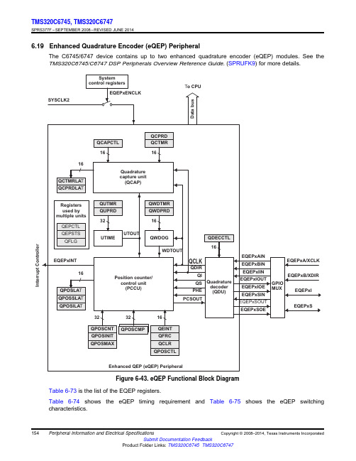
I n t e r r u p t C o n t r o l l e r 154TMS320C6745,TMS320C6747SPRS377F –SEPTEMBER 2008–REVISED JUNE 2014Submit Documentation FeedbackProduct Folder Links:TMS320C6745TMS320C6747Peripheral Information and Electrical Specifications Copyright ©2008–2014,Texas Instruments Incorporated6.19Enhanced Quadrature Encoder (eQEP)PeripheralThe C6745/6747device contains up to two enhanced quadrature encoder (eQEP)modules.See the TMS320C6745/C6747DSP Peripherals Overview Reference Guide.(SPRUFK9)for more details.Figure 6-43.eQEP Functional Block DiagramTable 6-73is the list of the EQEP registers.Table 6-74shows the eQEP timing requirement and Table 6-75shows the eQEP switching characteristics.PWM (A)TZ159TMS320C6745,TMS320C6747SPRS377F –SEPTEMBER 2008–REVISED JUNE 2014Submit Documentation FeedbackProduct Folder Links:TMS320C6745TMS320C6747Peripheral Information and Electrical SpecificationsCopyright ©2008–2014,Texas Instruments Incorporated 6.20.1Enhanced Pulse Width Modulator (eHRPWM)TimingPWM refers to PWM outputs on eHRPWM1-6.Table 6-77shows the PWM timing requirements and Table 6-78,switching characteristics.Table 6-77.eHRPWM Timing RequirementsPARAMETERTEST CONDITIONS MIN MAX UNIT t w(SYNCIN)Sync input pulse width Asynchronous2t c(SCO)cycles Synchronous 2t c(SCO)cyclesTable 6-78.eHRPWM Switching CharacteristicsPARAMETERTEST CONDITIONS MIN MAX UNIT t w(PWM)Pulse duration,PWMx output high/low 20ns t w(SYNCOUT)Sync output pulse width 8t c(SCO)cycles t d(PWM)TZA Delay time,trip input active to PWM forced highDelay time,trip input active to PWM forced lowno pin load;no additional programmable delay 25ns t d(TZ-PWM)HZ Delay time,trip input active to PWM Hi-Z no additionalprogrammable delay 20ns6.20.2Trip-Zone Input TimingA.PWM refers to all the PWM pins in the device.The state of the PWM pins after TZ is taken high depends on the PWMrecovery software.Figure 6-46.PWM Hi-Z CharacteristicsTable 6-79.Trip-Zone input Timing RequirementsPARAMETERMIN MAX UNIT t w(TZ)Pulse duration,TZx input low Asynchronous1t c(SCO)cycles Synchronous 2t c(SCO)cycles(1)MEP step size will increase with low voltage and high temperature and decrease with high voltage and cold temperature.Table 6-80shows the high-resolution PWM switching characteristics.Table 6-80.High Resolution PWM Characteristics at SYSCLKOUT =(60-100MHz)PARAMETERMIN TYP MAX UNIT Micro Edge Positioning (MEP)step size (1)200ps。
高电流系列芯片耐音器说明书
4532 (EIA 1812) 4.50±0.25 3.20±0.25
1.50±0.25
0.60±0.40
Ordering Information
WL
BD
1005 - 4532
Product Code
WL: Inductor
Series
BD: Chip Bead.
Dimensions JIS: (EIA) 1005 :(0402) 1608: (0603) 2012: (0805) 3216: (1206) 3225: (1210) 4516: (1806) 4532: (1812)
Impedance (Ω) +/-25%
Test
Frequency (MHz)
DC
Resistance (Ω) Max.
**WLBD1608HCU260TL
26
100
0.007
**WLBD1608HCU300TL **WLBD1608HCU700TL **WLBD1608HCU101TL **WLBD1608HCU121TL WLBD1608HCU221TL WLBD1608HCU331TL WLBD1608HCU471TL WLBD1608HCU601TL
Walsin Part Number
WLBD1608HCU300TH WLBD1608HCU600TH
33 60 120 Impedance (Ω) +/-25% 30
60
100 100 100 Test Frequency (MHz) 100
100
0.04 0.07 0.15 DC Resistance (Ω) max. 0.04
Page 3 of 16
华汕电子 13009A 晶体管芯片 产品说明书

NPN SILICON TRANSISTOR
13009A 晶体管芯片
█ 芯片简介
█ 管芯示意图
芯片尺寸:4 英寸(100mm) 芯片代码:D400AG-00 芯片厚度:240±20µm 管芯尺寸:4000×4000µm 2 焊位尺寸:B 极 783×1100µm 2,E 极 754×1276µm 2 电极金属:铝 背面金属:钒-镍-银 典型封装:KSH13009
最小值 400 10 6
4
典型值 180
最大值
1 40 30 1 1.5 3 1.2 1.6
1.1 3.0 0.7
单位 V mA
V V V V V pF MHz µS 0 VEB=9V,IC=0 VCE=5V,IC=5A VCE=5V,IC=8A IC=5A,IB=1A IC=8A,IB=1.6A IC=12A,IB=3A IC=5A,IB=1A IC=8A,IB=1.6A VCB=10V,f=0.1MHz VCE=10V,IC=0.5A
█ 极限值(Ta=25℃)(封装形式:TO-220)
Tstg——贮存温度………………………………… -65~150℃ Tj——结温……………………………………………… 150℃ PC——集电极耗散功率(Tc=25℃)………………… 100W VCBO——集电极—基极电压…………………………… 700V VCEO——集电极—发射极电压………………………… 400V VEBO——发射极—基极电压…………………………………9V IC——集电极电流(DC)…………………………………12A IB——基极电流………………………………………………6A
VCC=125V,IC=8A IB1=-IB2=1.6A
█ 电参数(Ta=25℃)(封装形式:TO-220)
PC792A1CC-12SD中文资料
Automotive Plug-In / PC B Power RelayFEATURESMost popular automotive relay1 A and 1 C contact forms ava ilable40 Amps continuous carrying c apacityContact switching capacity up to 120 Amps Up to 125 degrees C operating temperature Internal diodes or resisto rs availablePC792AMax. Switching Voltage 75 VDC1 Form A or 1 Form CCONTACT RATINGSCHARACTERISTICSOperate Time 7 ms. typical Release Time Insulation Resistance 5 ms. typical100 megohms min, at 500VDC, 50%R H Dielectric Strength 500 Vrms, 1 min. between coil and contacts Shock Resistance 20 g, 11ms, functional; 200 g, destructiveVibration Resistance Power Consumption 1.6 W approx.Ambient Temperature Range -40 to 85 degrees C operating, -40 to 125 degrees C for Class F Weight31 grams approx.ORDERING INFORMATIONExample:PC792A Model-12Sockets available from Picker C omponentsParallel Component-1C CONTACT DATAMaterialInitial Contact Resistance Service LifeMechanical ElectricalAgSnInO (Silver Tin Indium Oxide)100 milliohms max @ 0.1A, 6VDC 1 X 1072 X 105Operations OperationsNormally Open Nil: None; D: Diode; R: Resistor; N: N ickle Plated TerminalsCoil Voltage-C1Contact FormMax Switching Current Break 40 AmpsMake 120 Amps 60 Amps (at 20 degrees C)Max. Continuous Current Minimum Load0.1 A @ 12 VDC-RNDrop Resistance 1 Meter height drop on concrete in final enclosu re Normally Closed Break 30 AmpsMake 45 Amps 40 Amps (at 20 degrees C)Case StyleC: Plug-In; P: PCB; C1: Plastic Bracket; C 2: Metal Bkt DA 1.27 mm, 10 - 40 Hz; 40-70 Hz: 5 g; DA 0.5mm, 70-100 Hz; 100-500 Hz: 10 g.S EnclosureC: Dust Cover, S: Sealed CaseContact Form1A, 1C or 1U (1 form A with 2 #87 Termin als) 40 Amps (at 85 degrees C)30 Amps (at 85 degrees C)PC792APC792AREFERENCE CURVESCOIL DATACoil Voltage624Resistanceohms + 10%Must OperateVoltage Max.(VDC)Must Release Voltage Min.(VDC)Continuous Voltage Max.(VDC)22903307.214.31.22.420.539.1_ 3.60.610.112(17.9).705(8.4).331(16.9).665(8.0).3158787A308586(17.9).705(8.4).331(16.9).665(8.0).3158787A 308586(1.2 X 2.4).047 X .094All Holes3085Wiring Diagrams3085Form 1UForm 1AForm 1CDimensions in Inches (millimet ers)Plug-In TypeBottom View PC Board LayoutTolerances +.010 unless otherwise notedNotes:Maximum make current refers to inrush of a lamp load In 85 degree C ambient reduce maximum coil volt age to 72%Plug-In Case (C) and PCB Case (P)(24.5).965(26.5)1.04(26.5)1.04(6.3).250(11.5).453(0.8).031505560657075808590951001112131415161718AT 20 CoAT 85 CoAT 125 CoCoil Temp Rise Contacts Carrying 40AT e m p e r a t u r e R i s e Co405060708090100111213141516171820A30A 35A 40A Coil Temp RiseAmbient Temp 20 CoC o i l T e m p e r a t u r e R i s e CoCoil Applied VoltageCoil Applied Voltage121020353050100123101005203050N.O. Contact N.C. ContactMaximum Switching Capacity at 85 C Arc Extinguished Resistive LoadsSwitching Voltage(VDC)S w i t c h i n g C u r r e n t (A m p s )oPC792A PC792A(22.0).866(16.0).630(24.5).965(6.0).236(6.4).252 Dia.(26.5)1.04(26.5)1.04(4.2).165(26.5)1.04(26.5)1.04(16.0).630(24.5).965(15.0).591(6.0).236(5.3).210 Dia.(4.6).181(13.3).524(18.0).709(7.0).275.252 Dia.(6.4)(20.6).811(45.3)1.78(36.0)1.42(36.0)1.42(10.4).409Molded Plastic Bracket (C1)Bent Metal Bracket (C3)Metal Bracket (C2)Skirted Case with Metal Bracke t (C4)Skirted Case with Bent Metal B racket (C5)。
RH6015-C(D)原厂芯片应用指南规格书
RH6617_新版原厂规格书_Ver0.5
T.E.L:135.3045.2646单路输入双路输出触控型LED调光ICRH6617规格书Revision 0.5 2018-11-8目录1. 简介 (3)2. 特点 (3)3. 封装引脚示意图 (3)4. 功能描述 (4)4.1版本简述及模式配置 (4)4.2 输出模式 (4)4.1.1短按/长按 (4)4.1.2亮度记忆 (4)4.1.3渐明渐暗/突明突暗 (4)4.1.43级调光亮度 (5)4.1.5双输出模式控制流程 (5)5. 应用电路图 (5)6. PCB设计注意事项 (6)7. 电气参数 (6)7.1最大绝对额定值 (6)7.2DC/AC特性 (6)8. 封装信息 (8)8.1SOP8 (8)8.2DIP8 (9)1.简介RH6617是一款单路输入双路输出电容式触摸感应PWM调光IC。
RH6617可在有介质(如玻璃、亚克力、塑料、陶瓷等)隔离保护的情况下实现触摸功能,安全性高。
RH6617内置稳压源、上电复位/低压复位及环境自适应算法等多种措施,抗干扰性能优秀。
RH6617应用范围:触摸调光LED台灯、触摸调光LED壁灯或其他需要PWM 输出控制的触摸式产品。
2.特点工作电压:2.4V~5.5V待机平均电流:15uA@3V上电0.5s快速初始化环境自适应功能,可快速应对先上电后覆盖介质、触摸上电等类似应用场景可靠的上电复位(POR)及低压复位(LVR)性能 PWM输出频率24KHz(无级)、32KHz(三级调光),有效改善频闪封装形式:SOP8、DIP83.封装引脚示意图图1 SOP8/DIP8引脚示意图I-P H:带上拉电阻的CMOS输入I:CMOS输入O:推挽型CMOS输出I/O:CMOS输入/输出P:电源/地4.功能描述4.1版本简述及模式配置表2 版本型号列表型号无级调光初始亮度3级调光RH6617 100%,上电后第一次触摸开机亮度OFF/MAX/MID/MIN/OFF循环(1)注:1指配置为电源电压(VDD),0配置为0V电压。
MEMORY存储芯片MAX7219CWG中文规格书

rupt, the host (Bus Master) interrogates the bus slave devices via a special receive-byte operation that includes the alert response address. The data returned by this receive-byte operation is the address of the offending slave device. The interrupt pointer address can activate several different slave devices simultane-ously. If more than one slave attempts to respond, bus arbitration rules apply, with the lowest address code going first. The other device(s) will not generate an acknowledge and will continue to hold the ALERT line low or repeat the START-STOP interrupt until serviced.Clearing Interrupts via Alert ResponseWhen a fault occurs, ALERT asserts and latches low. Ifthe fault is momentary and disappears before the device is serviced, ALERT remains asserted. Normally,the master sends out the Alert Response address fol-lowed by a read bit (00011001). ALERT clears whenthe device responds by successfully putting its address on the bus. Reading the Alert Response address is the only method for clearing hardwareand software interrupt latches.Clearing the interrupthas no effect on the state of the status registers. MAX1661/MAX1662/MAX1663Serial-to-Parallel/Parallel-to-Serial Converters and Load-Switch Controllers with SMBus InterfaceFigure 3. SMB Serial-Interface Timing—Acknowledge and Data ValidFigure 4. I/O Read Timing DiagramM A X 1661/M A X 1662/M A X 1663START-STOP Software Interrupt The START-STOP interrupt is a method for the slave device to initiate a signal over the 2-wire interface with-out the need for a third (interrupt) wire. A START-STOP interrupt is a start condition followed by a stop condi-tion; in other words, SMBDATA goes low and then high with SMBCLK high (Figure 5 shows the START-STOP interrupt and a subsequent Alert Response transmis-sion used to clear the interrupt). The START-STOPfunction can be disabled (masked) by setting the dataregister mask SS (bit 6) high.In order to avoid bus collisions, the START-STOP inter-rupt will not occur when the bus is busy. If the devicebegins a start condition simultaneously with anothertransmitter on the bus, it recognizes the falling SMB-CLK as a collision and re-transmits the interrupt whenthe bus becomes available. Upon thermal shutdown ora transition on an I/O line, the device issues only oneSTART-STOP interrupt, and won’t repeat it unless therehas been a collision. However, thermal-shutdown faults,not being edge triggered, may result in a continuousstream of START-STOP bits.Input/Output PinsEach input/output (I/O) is protected by an internal20mA (typical) current-limit circuit. The I/O current limitdepends on the supply voltage and the voltage appliedto the I/O pins (see Typical Operating Characteristics ).The typical I/O bias current is 0.5µA to V I/O_= 28V.The ability of the I/Os to sink current depends on V CC as well as the voltage on the I/O. Typical pull-down on-resistance at V CC = 2.7V and 5.5V is 106Ωand 66Ω,respectively. I/O source and sink capability can affectthe rise and fall times of external power MOSFETs com-monly used in power-switching applications. Other fac-tors include the V GS , the input capacitance of the MOS-FET, and the pull-up resistor value used in the circuit.Typical MOSFET gate capacitance ranges from 150pF to 2000pF. Increasing the RC time constant slows down the MOSFET’s response, but provides for a smoother transition.Power-On Reset The power-on reset circuit keeps the external MOSFETs off during a power-up sequence. When the supply volt-age falls below the power-on reset threshold voltage,the MAX1662/MAX1663’s outputs reset to a high-impedance state, and the MAX1661’s outputs reset to a low state. During the initial power-up sequence, as V CC increases, the ALERT pin goes low and then high,which indicates the device is powered on. The time between the low and high state on ALERT is the power-on delay time. Below V CC = 0.8V (typical) the POR states can’t be enforced, and the I/O pins of all ver-sions exhibit increasingly weak pull-down current capa-bility, eventually becoming high impedance.Thermal Shutdown These devices have internal thermal-shutdown circuitry that turns off all output stages (I/O pins) when the junc-tion temperature exceeds +140°C typical. Thermal shutdown only occurs during an overload condition on the I/O pins. The device cycles between thermal shut-down and the overcurrent condition until the overload condition is removed. This could cause a sustained START-STOP interrupt and, in the extreme case, tie up the master controller. However, the device asserts ALERT low, indicating this fault status.Serial-to-Parallel/Parallel-to-Serial Converters and Load-Switch Controllers with SMBus InterfaceFigure 5. START-STOP Software Interrupt Timing Diagram and Alert Response。
奇立LED芯片10x23mil规格书(精)
Doc. No.制定日期 97年09月08日改訂日期 98年02月23日頁次 1 of 5 文件名稱10×23 Blue GaN LED Chip Standard Specifications (C-C4XXCPXXXX制定部門晶粒廠修訂紀錄修訂日期生效日期頁次版次制修記要修改者簽章 2008.02.12 All 01 新制定王富田 2008.05.01 All 02 新增光電特性量測條件及新增RoHS 標籤王富田2008.11.04 All 03 標籤代碼變更王富田 2009.02.232 04 內容變更王富田Doc. No.制定日期 97年09月08日改訂日期 98年02月23日頁次 2 of 5 文件名稱10×23 Blue GaN LED Chip Standard Specifications (C-C4XXCPXXXX制定部門晶粒廠1. ScopeThis specification sheet is only for Blue GaN CMLT C-C4□□CP □□□□ product.2. Material Structure & DimensionsMaterial structure : Sapphire P electrode (anode : Au alloy N electrode (cathode : Au alloy Chip thickness : 4 ± 1 mil3. Electro-Optical CharacteristicsTypical Iv tabl※Luminous intensity is measured with CMLT’S standard chip probin g equipment. Iv m※easure specification is ± 10% , λd measure specification is ± 1 nm Please contact us for available product※Value ParameterSymbolTest ConditionMin.Typ.Max.Unitλd If= 20 mA450 - 465 nm Iv If= 20 mA Refer to the Typical Iv tableRefer to the Typical Iv table mcd Vf If= 20 mA 2.8 3.2 3.5 V Ir Vr= -5V- - 1.0 uA ΔλΔλIf= 20 mA25nmValueSymbol Test ConditionMin.Typ.Max.UnitN 17 18.5 O 18.5 20P 20 21.5Q 21.5 23 R 23 24.5 Iv gradeS If= 20 mA26 30Po585 ± 20 umDoc. No.制定日期 97年09月08日改訂日期 98年02月23日頁次 3 of 5 文件名稱10×23 Blue GaN LED Chip Standard Specifications (C-C4XXCPXXXX制定部門晶粒廠4. Product Type No. Explanation for C-C4XXCPXXXXExample : C - (A. Standard chip product(B. Dominant Wavelength : 430 nm≦λd <490 nm with 2.5 nm interval when sorting, Other Wavelength are as follow table43 430 nm≦λd<440 nm 44 440 nm≦λd<450 nm 45 450 nm≦λd<460 nm 46 460 nm≦λd<470 nm 47 470 nm≦λd<480 nm 48 480 nm≦λd<490 nm(C. Luminous Intensity Grade : refer to the following tableFor Chip dimension < 400mil 2ABCDEFGHIJKLM0~ 55 ~ 5.5 5.5~6 6 ~ 6.5 6.5~7.5 7.5~ 8.5 8.5~ 9.5 9.5~10.5 10.5~11.5 11.5~12.5 12.5 ~14 14 ~15.5 15.5 ~17N O P Q R S T U V WX17~18.5 18.5~20 20~21.5 21.5~23 23~24.5 26 ~30 30~33.5 33.5 ~37 37 ~ 4141~ 4545 ~50(D.Chip Dimension : ( 10 mil x (23 mil A B C D E F G H I J K L M 891011121314151617181920N O P Q R S T U V W X Y Z 2121 222223232424262628283030323234343636383840404545(E. CMLT project code(F. Wavelength bin grade : 1 : 0~2.5nm, 2 : 2.5~5nm, 3 : 5~7.5nm, 4 : 7.5~10nm (G. CMLT project code (H.CMLT project code(G (A (B (C (E(D (F (HDoc. No.制定日期 97年09月08日改訂日期 98年02月23日頁次 4 of 5 文件名稱10×23 Blue GaN LED Chip Standard Specifications (C-C4XXCPXXXX制定部門晶粒廠5.Typical Electrical and Optical characteristic curves Test condition:Measured bare chip under Ta = 23℃±2℃Fig.1 Forward current vs. Forward voltage Fig.2 Relative Intensity vs. Forward CurrentFig.3 Spectrum vs. WavelengthDoc. No.制定日期 97年09月08日改訂日期 98年02月23日頁次 5 of 5 文件名稱10×23 Blue GaN LED Chip Standard Specifications (C-C4XXCPXXXX制定部門晶粒廠6. Label SheetA label sheet containing the detailed manufacturing information, such as Lot. number, type number, chip quantity, electro-optical characteristics, is pasted at the upper-left corner on blue tape . Standard dimension of the blue tape is equal to (190 ±10mm ×(190 ±10mm.7. Inspection ProcessAll of the chips are sorted into an array form on the blue sheet after 100% testing for electro-optical characteristics. Furthermore, 100% chip appearance inspection by optical microscope was performed in the standard manufacturing flow.21.2 21.8 22.3 455.5 456.2 457.32009/02/25Po。
南京时恒电子科技有限公司 MF52 系列测温型 NTC 热敏电阻器规格承认书说明书
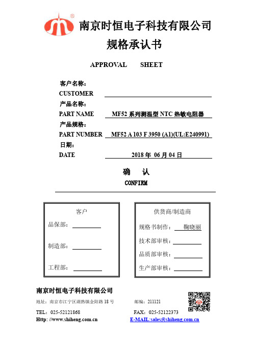
南京时恒电子科技有限公司规格承认书APPROVALSHEET客户名称:CUSTOMER 产品名称:PART NAME MF52系列测温型NTC 热敏电阻器产品规格:PART NUMBER MF52A 103F 3950(A1)(UL:E240991)日期:DATE2018年06月04日确认CONFIRM南京时恒电子科技有限公司地址:南京市江宁区湖熟镇金阳路18号邮编:211121TEL :************FAX :************E-MAIL:*****************.cn客户品保部:制造部:工程部:供货商/制造商规格书制作:鞠晓丽技术部审核:品质部审核:生产部审核:1.电气性能项目符号测试条件单位性能要求1.125℃的零功率电阻值R 25℃Ta=25±0.01℃测试功率≤0.1mw KΩ10KΩ±1%1.2B 值B 25/50B=[(T a ×T b )/(T b -T a )]×ln(R a /R b )T b =50℃±0.01℃K 3950±1%1.3耗散系数δ静止空气中mW/℃≥21.4时间常数τ静止空气中sec ≤71.5绝缘电阻/100V/DC 1minMΩ≥1001.6工作温度范围//℃-55℃~125℃1.7最大额定功率Pmax /mW501.8阻温特性///见附表11.9阻值误差///见附表2本规格书提供了南京时恒电子科技有限公司生产的MF52A 系列NTC 热敏电阻的结构尺寸、产品性能、试验条件、使用要求的描述,敬请贵司确认。
回传,若无回传,我司将视为默认。
贵公司改变产品用途,使用方法时,请与我们取得联系!客户名称:客户确认确认:时间:审核:时间:项目测试条件及方法技术要求2.1引出端强度固定电阻端,拉力:5±1N ,时间:10±1秒无可见性损伤R 25ΔR/R≤±2%2.2可焊性温度245±5℃时间2-3秒着锡面积≥95%2.3耐焊接热锡锅温度:260±5℃,浸入深度距电阻体6mm ,时间5±1秒R 25ΔR/R≤±2%2.4稳态湿热温度:40℃±2℃,湿度:93±2%,时间:500小时R 25ΔR/R≤±2%2.5温度快速变化-55℃30min→25℃5min→125℃30min→25℃5min,反复5次R 25ΔR/R≤±2%2.6高温储存温度:125℃±5℃时间:1000小时R 25ΔR/R≤±2%2.7低温储存温度:-55℃时间:1000小时R 25ΔR/R≤±2%MF52系列测温型NTC 热敏电阻器型号:MF52A 103F3950(A1)2.可靠性3、使用注意事项3.1本产品的用途:温度测量与控制;3.2避免流过热敏电阻芯片的电流引起元件自身发热而产生测量误差;3.3烙铁焊接时,焊接处距涂装层距离至少2mm,焊接温度应低于300℃,焊接时间<3ses;3.4储存温度:-10℃~40℃;储存湿度:≤75%RH;3.5避免存放在具有腐蚀性气体及光照的环境下;3.6包装打开后需重新密封保存。
电子元器件芯片AD8529AR中文规格书
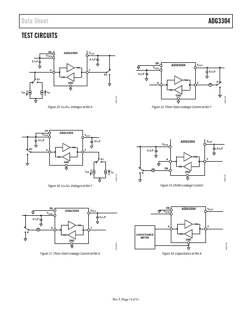
Data SheetADG3304 Rev. E | Page 13 of 21TEST CIRCUITSI OHFigure 29. V OH /V OL Voltages at Pin AI OL04860-044Figure 30. V OH /V OL Voltages at Pin Y 0Figure 31. Three-State Leakage Current at Pin AFigure 32. Three-State Leakage Current at Pin YFigure 33. EN Pin Leakage Current 04860-048Figure 34. Capacitance at Pin AADG3304Data Sheet Rev. E | Page 16 of 21TERMINOLOGYV IHALogic input high voltage at Pin A1 to Pin A4. V ILALogic input low voltage at Pin A1 to Pin A4. V OHA Logic output high voltage at Pin A1 to Pin A4. V OLA Logic output low voltage at Pin A1 to Pin A4. C A Capacitance measured at Pin A1 to Pin A4 (EN = 0). I LA, Hi-ZLeakage current at Pin A1 to Pin A4 when EN = 0 (high impedance state at Pin A1 to Pin A4).V IHYLogic input high voltage at Pin Y1 to Pin Y4. V ILYLogic input low voltage at Pin Y1 to Pin Y4. V OHY Logic output high voltage at Pin Y1 to Pin Y4. V OLY Logic output low voltage at Pin Y1 to Pin Y4. C Y Capacitance measured at Pin Y1 to Pin Y4 (EN = 0). I LY , Hi-ZLeakage current at Pin Y1 to Pin Y4 when EN = 0 (high impedance state at Pin Y1 to Pin Y4).V IHENLogic input high voltage at the EN pin. V ILENLogic input low voltage at the EN pin.C ENCapacitance measured at EN pin.I LENEnable (EN) pin leakage current.t ENThree-state enable time for Pin A1 to Pin A4 and Pin Y1 to Pin Y4.t P , A→YPropagation delay when translating logic levels in the A→Y direction.t R, A→YRise time when translating logic levels in the A→Y direction. T F, A→Y Fall time when translating logic levels in the A→Y direction. D MAX, A→Y Guaranteed data rate when translating logic levels in the A→Y direction under the driving and loading conditions specified in Table 1. T S KEW , A→Y Difference between propagation delays on any two channels when translating logic levels in the A→Y direction. t PPSKEW , A→Y Difference in propagation delay between any one channel and the same channel on a different part (under same driving/ loading conditions) when translating in the A→Y direction. t P , Y→A Propagation delay when translating logic levels in the Y→A direction. t R, Y→A Rise time when translating logic levels in the Y→A direction. t F, Y→A Fall time when translating logic levels in the Y→A direction. D MAX, Y→A Guaranteed data rate when translating logic levels in the Y→A direction under the driving and loading conditions specified in Table 1. t S KEW , Y→A Difference between propagation delays on any two channels when translating logic levels in the Y→A direction. t PPSKEW , Y→A Difference in propagation delay between any one channel and the same channel on a different part (under the same driving/ loading conditions) when translating in the Y→A direction. V CCA V CCA supply voltage. V CCY V CCY supply voltage. I CCA V CCA supply current. I CCY V CCY supply current. I Hi-Z, A V CCA supply current during three-state mode (EN = 0). I Hi-Z, Y V CCY supply current during three-state mode (EN = 0).。
芯片合格商品名单(QVL)标准表用户手册说明书

Qualified Vendors List (QVL) Standard table for user manualProject Name:A*B*C*256MB Kingston KVR333X64C25/256N/A Kingston SS D3208DH1T-6256MB Kingston KVR333X64C25/256N/A Hynix SS HY5DU56822BT-J Pass Fail 512MB Kingston KVR333X64C25/512N/A Hynix DS HY5DU56822BT-J Pass Pass 512MB Kingston KVR400X643A/512N/A Hynix DS HY5DU56822BT-D43PassPass512MB Kingston KVR400X64C3A/512N/A Kingston DS D3208DL3T-5256MB Kingston KVR400X64C3A/256N/A Hynix SS HY5DU56822BT-D43256MB Infineon HYS64D64320GU-5-C 3Infineon SS HYB25D256800CE-5C Pass Pass 512MB Infineon HYS64D32300GU-5-C 3Infineon DS HYB25D256800CE-5C Pass Pass256MB Infineon HYS64D64320GU-5-C N/A Infineon SS HYB25D256800CE-5C Fail 512MB Infineon HYS64D64320GU-6-CN/A Infineon DS HYB25D256800CE-6C Pass Pass 256MB HY DDR400-256N/A Hynix SS HY5DU56822BT-D43PassFail256MB HY DDR266-256N/A Hynix SS HY5DU56822AT-H 256MB HY DDR333-256N/A Hynix SS HY5DU56822BT-J Pass Pass 512MB HY DDR333-512N/A Hynix DS HY5DU56822BT-J 256MB Corsair VS256MB400N/A Value select SS VS32M8-5 2B0409Pass Pass 512MB Corsair VS512MB400N/A Value select DS VS32M8-5 2B0402Pass Fail 256MB Corsair VS256MB333N/A SAMSUNG SS K4H5608380-TCB3Pass Pass 512MB Corsair VS512MB333N/A Value select DS VS32M8-6 2B0412Pass Pass 512MB Micron MT16VDDT6464AG-335GB N/A MICRON DS MT46V32M8-G Pass Pass 256MB Micron MT8VDDT3264AG-335GB 2.5MICRON SS MT46V32M8-G Pass Pass 256MB Micron MT8VDDT3264AG-40BGB 3MICRON SS MT46V32M8-G Pass Pass 512MB Micron MT16VDDT6464AG-40BGB 3MICRON DS MT46V32M8-G 256MB Samsung M368L3223FTN-CCC 3SAMSUNG SS K4H560838F-TCCC Pass Pass 512MB Samsung M368L6423FTN-CCC N/A SAMSUNG DS K4H560838F-TCCC Pass Fail 256MB Samsung M368L3223FTN-CB3 2.5SAMSUNG SS K4H560838F-TCB3Pass Pass 512MB Samsung M368L6423FTN-CB3 2.5SAMSUNG DS K4H5608838F-TCB3Pass Pass 256MB Winbond U24256ADWBG6H20N/A Winbond SS W942508CH-5Pass Pass 256MB Winbond U24256AAWBG6H20N/A Winbond SS W942508CH-6Pass Fail 512MB Winbond DDR333-512N/A Winbond DS W942508BH-6Pass Pass 512MB Winbond U24512ADWBG6H20N/A Winbond DS W942508CH-5Pass Pass 256MB Elpida U24256AD1PG6H20N/A Elpida SS DD2508AKTA-5C Pass Fail 512MB Elpida U24512AD1PG6H20N/A Elpida DS DD2508AMTA Pass Pass 256MB Transcend DDR400-256N/A SAMSUNG SS K4H560838F-TCCC Pass Pass 256MB Transcend DDR400-256N/A Mosel SS V58C2256804SAT5B PassPass512MB Transcend DDR400-512N/A Mosel DS V58C2256804SAT5B 512MB Transcend DDR400-512N/A SAMSUNG DS K4H560838F-TCCC 512MB TranscendDDR333-512N/A Hynix DS HY5DU56822CT-J Pass Pass256MB Pmi 3208GATA07-04A7N/A Pmi SS PM4D328D50406EU 512MB Pmi 3208GATA01-04A4N/A Pmi DS PM4D328S50403DU 256MB Kingmax MPMB62D-38LT3R N/A Mosel SS V58C2256804SAT6Pass Fail 512MB Kingmax MPMC22D-38HT3R N/A Hynix DS HY5DU56822BT-J Pass Pass 256MB Kingmax MPMB62D-38KT3R N/A KINGMAX SS KDL388P4LA-50Pass Pass 512MB Kingmax MPXC22D-38KT3R N/A KINGMAX DS KDL388P4EA-50Pass Pass 256MB Mosel V826632K24SATG-D33Mosel SS V58C2256804SAT5Pass Pass 512MB Mosel V826664K24SATG-D33Mosel DS V58C2256804SAT5Pass Fail 256MB Nanya NT256D64S88B1G-5T 3Nanya SS NT5DS32M8BT-5T Pass Fail 512MB Nanya NT512D64S8HB1G-5T3Nanya DS NT5DS32M8BT-5T 256MB Apacer 77.10628.10A 2.5Apacer SS AM3A5608AIT-6B Pass Pass 512MB Apacer 77.90728.U1G 2.5Apacer DS AM3A568AJT-6B Pass Pass 512MB Apacer 77.10736.464 3SAMSUNG DS K4H560838E-TCCC 512MB Apacer 77.90739.U1G 2.5Apacer DS AM3A568AJT-5A Pass Pass 256MB Apacer 77.10636.46G 3SAMSUNG SS K4H560838E-TCCC 256MB Apacer 77.10636.56G3Mosel SS V58C2256804SAT5B Pass Fail 512MB Apacer 77.10736.11G 3Infineon DS HYB25D256800BT-5B Pass Fail 256MB Smart U24256ADSRG6H20N/A Smart SS D32M8XS50H3X4AMV Pass Fail 512MB Smart U24512ADSRG6H20N/A Smart DS D32M8XS50H3X4AMV Pass Pass 512MB Smart U24512ADSKG6H20N/A Smart DS D32M8XS60HBX4AMV1G Twinmos M2S5016AJAMC5G0811A-J N/A TWINMOS DS 46V64M8Pass Pass 512MB Twinmos M2S9J18BGAPS9F0811A-T 2.5PSC DS A2S56D30ATP 256MB A Data MDOSS1F3G3X10BZL0Z N/A SAMSUNG SS K4H560838E-TCC5PassPass512MBA DataMDOSS1F3H4X10BZL0ZN/ASAMSUNGDSK4H560838E-TCC5BrandSS/DSComponentDIMM socket support (Optional)SizeVendorModelCL512MB Promos V826662K24SCTG-D0 2.5Promos DS5B Pass Pass Note:A* : Supports one module inserted in any slot as Single-channel memory configurationB* : Supports one pair of modules inserted into eithor the blue slots or the black slots as one pair of Dual-channel memory configuration C* : Supports 4 modules inserted into both the blue and black slots as two pairs of Dual-channel memory configuration。
GW2ANR系列FPGA产品数据手册DS961-1.3说明书
GW2ANR系列FPGA产品数据手册DS961-1.3, 2023-02-27版权所有© 2023广东高云半导体科技股份有限公司、Gowin、晨熙、高云均为广东高云半导体科技股份有限公司注册商标, 本手册中提到的其他任何商标,其所有权利属其拥有者所有。
未经本公司书面许可,任何单位和个人都不得擅自摘抄、复制、翻译本文档内容的部分或全部,并不得以任何形式传播。
免责声明本文档并未授予任何知识产权的许可,并未以明示或暗示,或以禁止发言或其它方式授予任何知识产权许可。
除高云半导体在其产品的销售条款和条件中声明的责任之外,高云半导体概不承担任何法律或非法律责任。
高云半导体对高云半导体产品的销售和/或使用不作任何明示或暗示的担保,包括对产品的特定用途适用性、适销性或对任何专利权、版权或其它知识产权的侵权责任等,均不作担保。
高云半导体对文档中包含的文字、图片及其它内容的准确性和完整性不承担任何法律或非法律责任,高云半导体保留修改文档中任何内容的权利,恕不另行通知。
高云半导体不承诺对这些文档进行适时的更新。
目录目录 (i)图目录 (iv)表目录 (vi)1 关于本手册 (1)1.1 手册内容 (1)1.2 相关文档 (1)1.3 术语、缩略语 (2)1.4 技术支持与反馈 (3)2 产品概述 (4)2.1 特性概述 (4)2.2 产品信息列表 (6)3 结构介绍 (7)3.1 结构框图 (7)3.2 Memory (8)3.2.1 SDR SDRAM (8)3.2.2 NOR FLASH (9)3.3 可配置功能单元 (10)3.4 输入输出模块 (11)3.4.1 简介 (11)3.4.2 I/O电平标准 (12)3.4.3 I/O逻辑 (14)3.4.4 I/O逻辑工作模式 (16)3.5 块状静态随机存储器模块 (22)3.5.1 简介 (22)3.5.2 存储器配置模式 (23)3.5.3 存储器混合数据宽度配置 (24)3.5.4 校验位功能配置 (25)3.5.5 同步操作 (25)3.5.7 BSRAM操作模式 (25)3.5.8 时钟模式 (27)3.6 数字信号处理模块 (28)3.6.1 简介 (28)3.6.2 数据A、数据B和进位C的加法/减法运算DSP操作模式配置 (31)3.7 时钟 (32)3.7.1 简介 (32)3.7.2 全局时钟网络 (32)3.7.3 锁相环 (35)3.7.4 高速时钟 (37)3.7.5 DDR存储器接口时钟管理DQS (37)3.8 长线 (38)3.9 全局复置位 (38)3.10 编程配置 (38)3.11 片内晶振 (39)4 电气特性 (40)4.1 工作条件 (40)4.1.1 绝对最大范围 (40)4.1.2 推荐工作范围 (41)4.1.3 电源上升斜率 (41)4.1.4 热插拔特性 (42)4.1.5 POR特性 (42)4.2 ESD性能 (42)4.3 DC电气特性 (42)4.3.1 推荐工作范围DC电气特性 (42)4.3.2 静态电流 (44)4.3.3 I/O推荐工作条件 (44)4.3.4 单端I/O DC电气特性 (45)4.3.5 差分I/O DC电气特性 (46)4.4 AC开关特性 (47)4.4.1 CFU开关特性 (47)4.4.2 BSRAM开关特性 (47)4.4.3 DSP开关特性 (47)4.4.4 Gearbox开关特性 (47)4.4.5 时钟和I/O开关特性 (47)4.4.7 锁相环开关特性 (48)4.5 编程接口时序标准 (48)5 器件订货信息 (49)5.1 器件命名 (49)5.2 器件封装标识示例 (50)图目录图3-1结构概念示意图 (7)图3-2 CFU结构示意图 (10)图3-3 IOB结构示意图 (11)图3-4 GW2ANR系列FPGA产品I/O Bank分布示意图 (12)图3-5 I/O逻辑输出示意图 (14)图3-6 I/O逻辑输入示意图 (14)图3-7 IODELAY示意图 (15)图3-8 GW2ANR的I/O寄存器示意图 (15)图3-9 GW2ANR的IEM示意图 (16)图3-10普通模式下的I/O逻辑结构示意图 (16)图3-11 SDR模式下的I/O逻辑结构示意图 (17)图3-12 I/O逻辑的DDR输入示意图 (17)图3-13 I/O逻辑的DDR输出示意图 (17)图3-14 I/O逻辑的IDES4输入示意图 (18)图3-15 I/O逻辑的OSER4输出示意图 (18)图3-16 I/O逻辑的IVideo输入示意图 (18)图3-17 I/O逻辑的OVideo输出示意图 (19)图3-18 I/O逻辑的IDES8输入示意图 (19)图3-19 I/O逻辑的OSER8输出示意图 (19)图3-20 I/O逻辑的IDES10输入示意图 (19)图3-21 I/O逻辑的OSER10输出示意图 (20)图3-22 IO逻辑的IDDR_MEM输入示意图 (20)图3-23 IO逻辑的ODDR_MEM输出示意图 (20)图3-24 IO逻辑的IDES4_MEM输入示意图 (21)图3-25 IO逻辑的OSER4_MEM输出示意图 (21)图3-26 IO逻辑的IDES8_MEM输入示意图 (21)图3-27 IO逻辑的OSER8_MEM输出示意图 (22)图3-28单端口、伪双端口及双端口模式下的流水线模式 (26)图3-29独立时钟模式 (27)图3-30读写时钟模式 (27)图3-31单端口时钟模式 (28)图3-32 DSP宏单元 (29)图3-33 GW2ANR时钟资源 (32)图3-34 GCLK象限分布示意图 (33)图3-35 DQCE结构示意图 (34)图3-36 DCS接口示意图 (34)图3-37 DCS Rising Edge模式下的时序示意图 (34)图3-38 DCS Falling Edge模式下的时序示意图 (35)图3-39 PLL示意图 (35)图3-40 GW2ANR HCLK示意图 (37)图3-41 DQS示意图 (38)图5-1器件命名方法–ES (49)图5-2器件命名方法–Production (49)图5-3器件封装标识示例 (50)表目录表1-1术语、缩略语 (2)表2-1产品信息列表 (6)表2-2 GW2ANR-18列表 (6)表3-1 GW2ANR系列FPGA产品支持的输出I/O类型及部分可选配置 (13)表3-2 端口介绍 (14)表3-3 BSRAM信号功能 (23)表3-4存储器配置列表 (23)表3-5双端口混合读写数据宽度配置列表 (24)表3-6伪双端口混合读写数据宽度配置列表 (25)表3-7时钟模式配置列表 (27)表3-8 DSP端口描述 (29)表3-9内部寄存器描述 (30)表3-10 PLL端口定义 (36)表3-11片内晶振的输出频率选项 (39)表4-1绝对最大范围 (40)表4-2推荐工作范围 (41)表4-3电源上升斜率 (41)表4-4热插拔特性 (42)表4-5 POR电压标准 (42)表4-6 GW2ANR ESD - HBM (42)表4-7 GW2ANR ESD - CDM (42)表4-8推荐工作范围内DC电气特性 (42)表4-9静态电流 (44)表4-10 I/O推荐工作条件 (44)表4-11单端I/O DC电气特性 (45)表4-12差分I/O DC电气特性 (46)表4-13 CFU时序参数 (47)表4-14 BSRAM时序参数 (47)表4-15 DSP时序参数 (47)表4-16 Gearbox时序参数 (47)表4-17外部开关特性 (47)表4-18片内晶振特性参数 (48)表4-19 PLL特性参数 (48)1关于本手册 1.1手册内容1关于本手册1.1手册内容GW2ANR系列FPGA产品数据手册主要包括高云半导体GW2ANR系列FPGA产品特性概述、产品资源信息、内部结构介绍、电气特性、编程接口时序以及器件订货信息,帮助用户快速了解高云半导体GW2ANR系列FPGA产品以及特性,有助于器件选型及使用。
艾瓦特芯片规格书

艾瓦特芯片规格书如下:一、产品概述艾瓦特芯片是专为高性能计算和人工智能应用设计的高端芯片。
它采用最先进的7纳米工艺制造,具有高性能、低功耗和低热量排放的特点。
艾瓦特芯片支持并行计算,可以高效处理大规模数据和算法,是提高计算性能的关键组件。
二、技术规格1. 工艺技术:7纳米工艺制造2. 核心数量:双核心3. 内存带宽:高达51.2GB/s4. 计算能力:强大的计算能力,适用于高性能计算和人工智能应用5. 能耗:低功耗设计,适合节能环保6. 热量排放:先进的散热技术,确保芯片在高负荷运行时稳定可靠7. 工作温度:工作温度范围宽广,适应各种环境和使用场景三、性能特点1. 高性能:艾瓦特芯片采用并行计算架构,可高效处理大规模数据和算法,提高计算性能。
2. 高效能比:在相同的计算任务下,艾瓦特芯片的性能比传统处理器高得多。
3. 节能环保:低功耗设计和先进的散热技术,确保芯片在长时间运行和高温环境下稳定可靠。
4. 兼容性:艾瓦特芯片兼容现有的软件和硬件系统,方便用户使用。
四、应用领域艾瓦特芯片适用于各种高性能计算和人工智能应用,如大数据分析、云计算、机器学习和深度学习等。
它能够为各种应用提供强大的计算能力,提高工作效率和性能比。
五、生产与品质艾瓦特芯片采用最先进的生产工艺,确保产品的高品质和高稳定性。
我们的质量控制流程严格遵循行业标准,从原料到成品进行全面检测,确保产品的性能和质量达到最高水平。
六、服务与支持我们提供全面的售后服务和技术支持,包括产品咨询、故障排除、解决方案提供等。
我们承诺在第一时间解决客户的问题,确保客户的利益和满意度。
以上就是艾瓦特芯片的规格书,我们致力于为客户提供高性能、稳定可靠的产品,帮助客户实现更高的计算性能和效率。
锐尔威视A63-Core产品硬件手册说明书
A63-Core 产品硬件手册2020-5-28 Ver.C锐尔威视版本更新说明1. 产品概述1.1 产品简介锐尔威视的A63-Core模块是基于全志A63平台设计的高性价比嵌入式核心模块板。
A63-Core采用130pin邮票孔封装形式,六层高速PCB设计,体积非常小,适合做手持便携类产品。
A63-Core模块集成2GB LPDDR3内存和16GB EMMC存储器,集成PMU芯片,带电池充放电管理。
集成音频Codec功能,GPU为Mali-T760,可满足人脸识别及AI算法的需求,支持硬解H.265/H.264 4K@30fps,提供丰富的外设资源:USB、UART、SDIO、SPI、IIC、GPIO。
支持驱动2个4-lane MIPI 或1个8-lane MIPI接口的显示屏,最大分辨率2560x1600,支持驱动2-lane EDP屏,分辨率1920x1080。
搭载Android7.1操作系统,经过深度优化定制,运行流畅,用户可由PC端的固件修改工具定制个性化固件,如修改开机图片动画声音、设置开机自启动应用、更改LCD屏配置、设置屏幕旋转方向、修改机器信息等1.2 产品规格2. 应用接口2.1 邮票孔接口A63-Core采用邮票孔封装,间距1.2mm,共130个引脚2.1.1 管脚分布2.1.2 管脚定义2.2 电源2.2.1 DC供电A63-Core模块用直流5V电源供电,上电即可开机,电压范围4.8~6V。
用户根据应用场合,选择使用12V或24V降压DC/DC设计电源为保证系统的稳定运行,电源输入处的滤波电容建议不小于100uF。
具体要根据产品应用场合和经验选择合适的电容值2.2.2 电池充电和电池管理使用3.7V锂电池供电A63-Core内置线性充电管理电路,支持对3.7V锂电池进行充电。
支持DC和USB接口充电,当两种充电口同时接通时,优先选择DC充电如需要使用电池给外设(屏,USB)供电,建议用PS接升压IC,升压到5V2.2.3 RTC电源内部VRTC耗电较大,不建议使用,需要使用外挂RTC芯片(PCF8563),软件默认支持外挂RTC。
H7920产品手册
第三章 路由器配置.................................................................................. 23
3.1 设置连接............................................................................................................................... 23 3.2 参数配置.................................................................................................. 27 3.2.1 查看系统工作状态 ....................................................................................................... 30 3.2.2 在线帮助....................................................................................................................... 31 3.2.3 系统工具....................................................................................................................... 32 3.2.4 网络参数配置............................................................................................................... 38 3.2.5 路由参数配置............................................................................................................... 46 3.2.6 特殊应用参数配置 ....................................................................................................... 51 3.2.7 宏电产品目录............................................................................................................... 56 3.2.8 注销............................................................................................................................... 57 3.2.9 系统升级....................................................................................................................... 57
FPGA可编程逻辑器件芯片EP4CGX50DF27C8N中文规格书
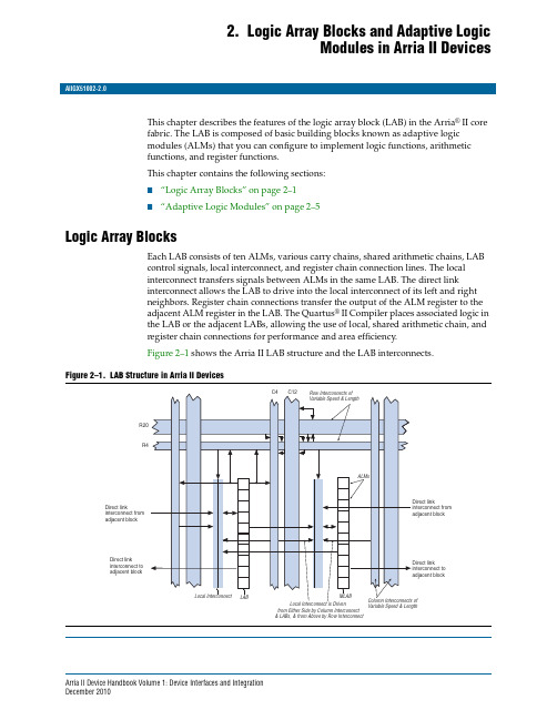
Arria II Device Handbook Volume 1: Device Interfaces and Integration December 2010 2.Logic Array Blocks and Adaptive LogicModules in Arria II DevicesThis chapter describes the features of the logic array block (LAB) in the Arria ®II core fabric. The LAB is composed of basic building blocks known as adaptive logic modules (ALMs) that you can configure to implement logic functions, arithmetic functions, and register functions.This chapter contains the following sections:■“Logic Array Blocks” on page 2–1■“Adaptive Logic Modules” on page 2–5Logic Array BlocksEach LAB consists of ten ALMs, various carry chains, shared arithmetic chains, LAB control signals, local interconnect, and register chain connection lines. The local interconnect transfers signals between ALMs in the same LAB. The direct link interconnect allows the LAB to drive into the local interconnect of its left and right neighbors. Register chain connections transfer the output of the ALM register to the adjacent ALM register in the LAB. The Quartus ® II Compiler places associated logic in the LAB or the adjacent LABs, allowing the use of local, shared arithmetic chain, and register chain connections for performance and area efficiency.Figure 2–1 shows the Arria II LAB structure and the LAB interconnects.Figure 2–B Structure in Arria II Devicesb lockb lockVa r iable S peed & Le n gth f r om Eithe r S ide by Colum n I n te r co nn ect& LAB s , & f r om Above by Row I n te r co nn ectDirect linkinterconnect fromadjacent b lock Direct linkinterconnect toadjacent b lockChapter 2:Logic Array Blocks and Adaptive Logic Modules in Arria II DevicesAdaptive Logic ModulesCarry ChainThe carry chain provides a fast carry function between the dedicated adders inarithmetic or shared arithmetic mode. The two-bit carry select feature in Arria IIdevices halves the propagation delay of carry chains within the ALM. Carry chainscan begin in either the first ALM or the fifth ALM in a LAB. The final carry-out signalis routed to an ALM, where it is fed to local, row, or column interconnects.The Quartus II Compiler automatically creates carry chain logic during designprocessing, or you can create it manually during design entry. Parameterizedfunctions such as LPM automatically take advantage of carry chains for theappropriate functions.The Quartus II Compiler creates carry chains longer than 20 ALMs (10 ALMs inarithmetic or shared arithmetic mode) by linking LABs together automatically. Toenhance fitting, a long carry chain runs vertically, allowing fast horizontal connectionsto TriMatrix memory and DSP blocks. A carry chain can continue as far as a fullcolumn.To avoid routing congestion in one small area of the device when a high fan-inarithmetic function is implemented, the LAB can support carry chains that only useeither the top half or bottom half of the LAB before connecting to the next LAB. Thisleaves the other half of the ALMs in the LAB available for implementing narrowerfan-in functions in normal mode. Carry chains that use the top five ALMs in the firstLAB carry into the top half of the ALMs in the next LAB in the column. Carry chainsthat use the bottom five ALMs in the first LAB carry into the bottom half of the ALMsin the next LAB within the column. In every alternate LAB column, the top half can bebypassed; in the other MLAB columns, the bottom half can be bypassed.1For more information on carry chain interconnect, refer to “ALM Interconnects” on page2–17.Arria II Device Handbook Volume 1: Device Interfaces and IntegrationChapter 3:Memory Blocks in Arria II DevicesMemory ModesMemory ModesArria II memory blocks allow you to implement fully synchronous SRAM memory inmultiple modes of operation. M9K and M144K blocks do not support asynchronousmemory (unregistered inputs). MLABs support asynchronous (flow-through) readoperations.Depending on which memory block you target, you can use the following modes:■“Single-Port RAM Mode” on page3–10■“Simple Dual-Port Mode” on page3–12■“True Dual-Port Mode” on page3–15■“Shift-Register Mode” on page3–17■“ROM Mode” on page3–18■“FIFO Mode” on page3–181To choose the desired read-during-write behavior, set the read-during-write behavior to either new data, old data, or don't care in the RAM MegaWizard Plug-In Managerin the Quartus II software. For more information about this behavior, refer to“Read-During-Write Behavior” on page3–21.1When using the memory blocks in ROM, single-port, simple dual-port, or truedual-port mode, you can corrupt the memory contents if you violate the setup or holdtime on any of the memory block input registers. This applies to both read and writeoperations.Single-Port RAM ModeAll memory blocks support single-port mode. Single-port mode allows you to doeither a one-read or a one-write operation at a time. Simultaneous reads and writesare not supported in single-port mode. Figure3–9 shows the single-port RAMconfiguration.Figure3–9.Single-Port Memory (Note1)Note to Figure3–9:(1)You can implement two single-port memory blocks in a single M9K and M144K blocks. For more information, referto “Packed Mode Support” on page3–5.Arria II Device Handbook Volume 1: Device Interfaces and Integration。
- 1、下载文档前请自行甄别文档内容的完整性,平台不提供额外的编辑、内容补充、找答案等附加服务。
- 2、"仅部分预览"的文档,不可在线预览部分如存在完整性等问题,可反馈申请退款(可完整预览的文档不适用该条件!)。
- 3、如文档侵犯您的权益,请联系客服反馈,我们会尽快为您处理(人工客服工作时间:9:00-18:30)。
2.84 2.84
单位 V V uA uA V V
湖南融和微电子有限公司
RH792A_SPEC_Ver1.0
6/7页
7/6/2015
8.封装信息
8.1 SOT23-6L
RH792A_SPEC
图 4 SOT23-6L封装图
表 7 SOT23-6L封装尺寸
符号
尺寸(mm单位) 最小值 典型值 最大值
符号
协议 可靠的上电复位(POR)及低压复位(LVR)性能 封装及脚位绑定:SOT23-6
1 DP1 2 GND 3 DP2
DM1 6 VDD 5 DM2 4
RH792A
图 1 引脚示意图
表 1 产品说明
No. 产品型号
产品封装
协议端口数
支持Apple设备最大功率协议 (注1*)
1
RH792A
SOT23-6L
工作电流
正常模式
IDD
LVR复位(*)
DP/DM 电压
VDP VDM
VDD =5.0v
2.57 2.57
若无特别说明,VDD为5.0V,环境温度为25℃,输出无负载
注*:LVR复位模式时,USB充电协议端口控制功能被关闭。
RH792A_SPEC
典型值 5.0 4.0 140 55 2.7 2.7
最大值 5.5
支持最大功率为10W/5W的Divider1苹果设备。
5.2 Divider模式设定
定义12W充电器,DP/DM与USB端子D+/D-端连接方式无要求。
湖南融和微电子有限公司
RH792A_SPEC_Ver1.0
4/7页
7/6/2015
6.应用电路图
RH792A_SPEC
USB Connector
5V Power
尺寸(mm单位) 最小值 典型值 最大值
A
2.82
-
3.02
D1
0.40
-
0.50
A1
0.90
-
1.00
D2
-
0.254
-
A2
0.35
-
0.45
D3
0.60
-
0.70
B
1.52
-
1.72
θ
-
9°
-
B1
2.80
-
3.00
θ1
-
10°
-
B2
0.119
-
0.135
θ2
C
1.05
-
1.15
θ3
-
0~8°
-
-
损坏 IC,主要起限流作用,建议取值 R=750 欧左右;C 主要用来补偿 R 对电源纹波的影响,也可以 不要。
7.电气参数
7.1 最大绝对额定值
表 5 最大绝对额定值
项目 (DP/DM,HBM)
符号 VDD
VI / VO TOPR TSTG VESD
1 DP1 2 GND 3 DP2
RH792A
DM1 6 VDD 5 DM2 4
VBUS VBUS
D-
D+
0.5K~1K
R C 1uF
GND
VBUS D-
D+
GND
Divider3 12W: DP/DM与D+/D-连接顺序无要求
USB Connector
图 3 RH792A电路示意图 说明: 1. 图中虚线框内的 R 是为了防止前级供电的 AC-DC 的输出电压过冲到 5V 以上,例如 7V,甚至到 9V
7/6/2015
表 2 引脚描述表 引脚名称
DP1 GND DP2 DM2 VDD DM1 I:CMOS输入 I/O:CMOS输入/输出
RH792A
1 2 3 4 5 6
RH792A_SPEC
I/O
功能描述
I/O 连接至第一组 USB 端口 DP
P
负电源
I/O 连接至第二组 USB 端口 DP
I/O 连接至第二组 USB 端口 DM
3.封装引脚示意图
2.特性
RH792A_SPEC
工作电压:4.5V~5.5V 双端口控制功能:可同时独立支持两路 USB 充
电协议检测 支持多种USB充电协议,各充电协议自动切换,
包括: Divider1/Divider2/Divider3充电协议(苹果
专用) D+/D–置1.2V模式(三星专用) BC1.2 DCP及CTIS YD/T 1591-2009充电
P
正电源
I/O 连接至第一组 USB 端口 DM
O:推挽型CMOS输出
P:电源/地
4.定购信息
表 3 定购信息 产品型号 RH792A
产品封装 SOT23-6L
包装/数量 Tape and Reel / 3000 units
产品印章
RH792A X Wxxxx
5.功能描述
5.1 USB协议支持
表 4 对应支持的USB协议:
深圳芯派科技 TEL:135 3045 2646 (唐生) ICQ:294 4345 3362
RH792A_SPEC
USB 充电协议端口控制器
RH792A
规格书
Revision 1.0 2015-7-6
湖南融和微电子有限公司
RH792A_SPEC_Ver1.0
1/7页
7/6/2015
RH792A_SPEC
NO
USB 充电
1
协议
2
支持
3
4
USB 协议
Divider 3(注 1*) D+/D-置 1.2V BC1.2 DCP CTIS YD/T 1591-2009
USB 端子 D+
2.7 1.2 短接
短接
USB 端子 D-
2.7 1.2 短接
短接
最大 功率
12W
792A
√ √ √ √
注1*:苹果设备的DividerX模式向下兼容DividerX-1模式,既支持最大功率12W的Divider2苹果设备,也
2
12W(Divider3)
注1*:5W、10W、12W仅针对Apple系列设备区分,各型号对非Apple系列设备的支持无区别;苹果协议
是向下兼容苹果设备的,即设置12W协议时(Divider3),兼容12W/10W/5W的苹果设备。
湖南融和微电子有限公司
RH792A_SPEC_Ver1.0
3/7页
湖南融和微电子有限公司
RH792A_SPEC_Ver1.0
2/7页
7/6/2015
1.简介
RH792A是USB充电协议端口控制IC,可自动识别 充电设备类型,并通过对应的USB充电协议与设备握 手,使之获得最大充电电流,在保护充电设备的前提 下节省充电时间。 应用范围:移动电源、便携式充电器、车载充电器 等。
目录
1. 简介 .............................................................................................................................................. 3 2. 特性 .............................................................................................................................................. 3 3. 封装引脚示意图 ............................................................................................................................. 3 4. 定购信息 ....................................................................................................................................... 4 5. 功能描述 ....................................................................................................................................... 4