NST3946DP6T5G;中文规格书,Datasheet资料
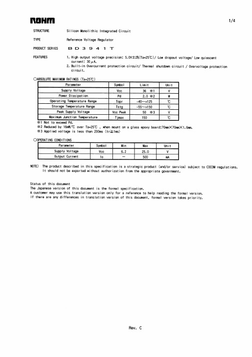
BD3941T中文资料
TEL : +33(0)1 56 97 30 60 FAX : +33(0) 1 56 97 30 80 TEL : +852(2)740-6262 TEL : +86(21)6279-2727 TEL : +86(411)8230-8549 TEL : +86(10)8525-2483 TEL : +866(2)2500-6956 TEL : +82(2)8182-700 TEL : +65-6332-2322 TEL : +60(3)7958-8355 TEL : +63(2)807-6872 TEL : +66(2)254-4890 FAX : +852(2)375-8971 FAX : +86(21)6247-2066 FAX : +86(411)8230-8537 FAX : +86(10)8525-2489 FAX : +866(2)2503-2869 FAX : +82(2)8182-715 FAX : +65-6332-5662 FAX : +60(3)7958-8377 FAX : +63(2)809-1422 FAX : +66(2)256-6334
(Contact address for overseas customers in Japan)
Yokohama
As of 18th. April 2005
Please contact our sales offices for details ;
U.S.A / San Diego Atlanta Dallas Germany / Dusseldorf TEL : +1(858)625-3630 TEL : +1(770)754-5972 TEL : +1(972)312-8818 TEL : +49(2154)9210 FAX : +1(858)625-3670 FAX : +1(770)754-0691 FAX : +1(972)312-0330 FAX : +49(2154)921400 FAX : +44(1)908-282-528
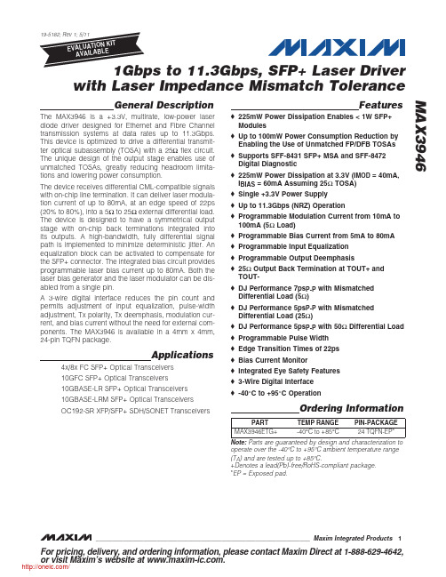
MAX3946ETG+T;MAX3946ETG+;中文规格书,Datasheet资料
Stresses beyond those listed under “Absolute Maximum Ratings” may cause permanent damage to the device. These are stress ratings only, and functional operation of the device at these or any other conditions beyond those indicated in the operational sections of the specifications is not implied. Exposure to absolute maximum rating conditions for extended periods may affect device reliability.
19-5182; Rev 1; 5/11
TION KIT EVALUA BLE AVAILA
1Gbps to 11.3Gbps, SFP+ Laser Driver with Laser Impedance Mismatch Tolerance
General Description
The MAX3946 is a +3.3V, multirate, low-power laser diode driver designed for Ethernet and Fibre Channel transmission systems at data rates up to 11.3Gbps. This device is optimized to drive a differential transmitter optical subassembly (TOSA) with a 25I flex circuit. The unique design of the output stage enables use of unmatched TOSAs, greatly reducing headroom limitations and lowering power consumption. The device receives differential CML-compatible signals with on-chip line termination. It can deliver laser modulation current of up to 80mA, at an edge speed of 22ps (20% to 80%), into a 5I to 25I external differential load. The device is designed to have a symmetrical output stage with on-chip back terminations integrated into its outputs. A high-bandwidth, fully differential signal path is implemented to minimize deterministic jitter. An equalization block can be activated to compensate for the SFP+ connector. The integrated bias circuit provides programmable laser bias current up to 80mA. Both the laser bias generator and the laser modulator can be disabled from a single pin. A 3-wire digital interface reduces the pin count and permits adjustment of input equalization, pulse-width adjustment, Tx polarity, Tx deemphasis, modulation current, and bias current without the need for external components. The MAX3946 is available in a 4mm x 4mm, 24-pin TQFN package.
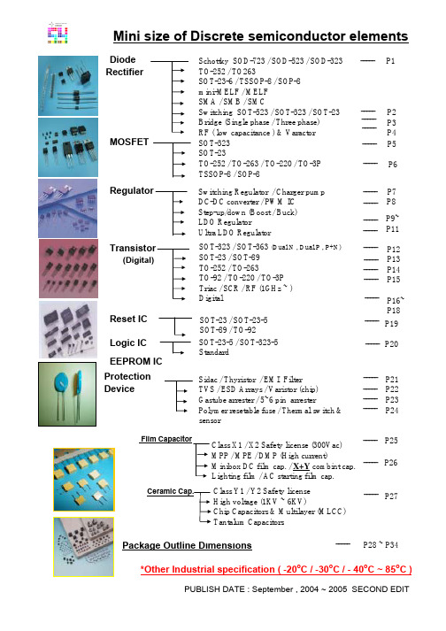
MMDT3946中文资料
N+P
N+P
SOT-23 (P.28)
BC807 BC817 BC846 BC847 BC848 BC856 BC857 BC858 BCW65C MMBT1015 MMBT1815 MMBT2222A MMBT2369 MMBT2484 MMBT2907A MMBT3904 MMBT3906 MMBT4124 MMBT4125 MMBT4401 MMBT4403 MMBT5086 MMBT5087 MMBT5088 MMBT5089 MMBT5401 MMBT5550 MMBT5551 MMBT6427 MMBT6429 MMBT6517 MMBT6520 MMBT8050 MMBT8099 MMBT8550 MMBT8599 MMBT9018 MMBTA06 MMBTA13 MMBTA14
Ceramic Ckage Outline Dimensions
P28 ~ P34
o o
*Other Industrial specification ( -20 C / -30 C / - 40 C ~ 85 C )
PUBLISH DATE : September , 2004 ~ 2005 SECOND EDIT
BCE BCE BCE BCE BCE BCE BCE BCE DAUL DAUL DAUL DAUL DAUL DAUL DAUL DAUL
N+P
SOT-363 (P.29)
MMDT2412 MMDT3904 MMDT2222 MMDT2411 MMDT1036 MMDT1037 MMDT3906 MMDT2907 MMDT2227 MMDT3946
PNP NPN NPN NPN NPN PNP PNP PNP NPN PNP NPN NPN NPN NPN PNP NPN PNP NPN PNP NPN PNP PNP PNP NPN NPN PNP NPN NPN NPN NPN NPN PNP NPN NPN PNP PNP NPN NPN NPN NPN -50 50 80 50 30 -80 -50 -30 60 -50 60 75 40 60 -60 60 -40 30 -30 60 -40 -50 -50 35 30 -160 160 180 40 55 350 -350 25 80 -25 -80 20 80 30 30 -45 45 65 45 30 -65 -45 -30 32 -50 50 40 40 60 -60 40 -40 25 -30 40 -40 -50 -50 30 25 -150 140 160 40 45 350 -350 20 80 -20 -80 15 80 30 30 -800 800 100 100 100 -100 -100 -100 800 -150 150 600 500 50 -600 200 -200 200 -200 600 -600 -50 -50 50 50 -600 600 600 500 200 500 -500 700 500 -700 -500 50 500 300 300 225 225 225 225 225 225 225 225 225 225 225 225 225 225 225 225 225 225 225 225 225 225 225 225 225 225 225 225 225 225 225 225 225 225 225 225 225 225 225 225 100 100 110 110 110 115 110 110 250 120 120 100 40 250 100 100 120 120 50 100 100 150 250 300 400 60 60 80 20K 500 30 30 150 100 150 100 30 50 10K 20K 630 630 800 800 800 800 800 800 630 700 700 300 120 300 300 360 360 150 300 300 500 800 900 1200 240 250 250 200K 1250 200 200 500 300 400 300 400 -100 100 2 2 2 -2 -2 -2 100 -2 2 150 10 1 -150 10 -10 2 -2 150 -150 -0.1 -0.1 0.1 0.1 -10 10 10 100 0.1 30 -30 150 1 -150 -1 1 10 100 100 -1 1 5 5 5 -5 -5 -5 1 -6 6 10 1 5 -10 1 -1 1 -1 1 -2 -5 -5 5 5 -5 5 5 5 5 10 -10 1 5 -1 -5 6 1 5 5 -0.7 0.7 0.25 0.25 0.25 -0.3 -0.3 -0.3 0.3 -0.3 0.25 0.5 0.25 0.35 -0.4 0.2 0.25 0.3 -0.4 0.4 -0.4 -0.3 -0.3 0.5 0.5 -0.2 0.25 0.15 1.2 0.2 0.5 -0.5 0.5 0.4 -0.5 -0.4 0.5 0.25 1.5 1.5 -500 500 10 10 10 -10 -10 -10 100 -100 100 380 10 1 -150 10 -10 50 -50 150 -150 -10 -10 10 10 -10 50 10 50 10 30 -30 500 100 -500 -100 5 100 100 100 -50 50 0.5 0.5 0.5 -0.5 -0.5 -0.5 10 -10 10 10 1 0.1 -15 1 -1 5 -5 15 -15 -1 -1 1 1 -1 5 1 0.5 0.5 3 -3 50 5 -50 -5 0.5 10 0.1 0.1 100 40 40 150 150 150 150 500 100 125 125 200 300 250 300 200 250 200 40 40 50 50 100 100 100 100 100 300 300 300 150 150 150 170 80 80 300 500
LT3956EUHE#PBF;LT3956EUHE#TRPBF;LT3956IUHE#PBF;LT3956IUHE#TRPBF;中文规格书,Datasheet资料
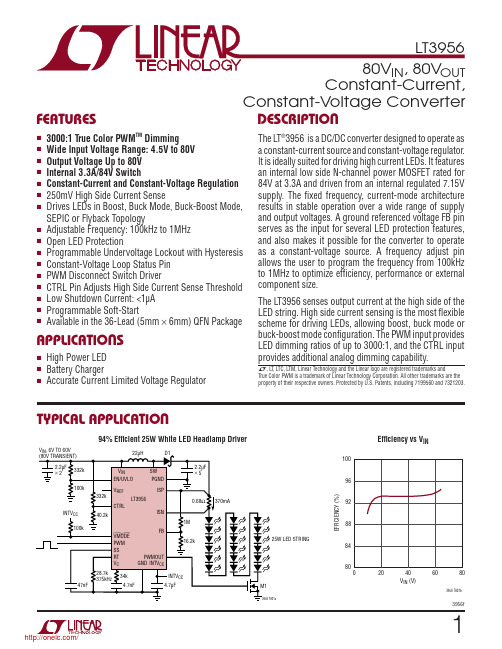
3956fTypical applicaTionFeaTuresapplicaTionsDescripTionConstant-Current,Constant-Voltage Converter The L T ®3956 is a DC/DC converter designed to operate as a constant-current source and constant-voltage regulator . It is ideally suited for driving high current LEDs. It features an internal low side N-channel power MOSFET rated for 84V at 3.3A and driven from an internal regulated 7.15V supply. The fixed frequency, current-mode architecture results in stable operation over a wide range of supply and output voltages. A ground referenced voltage FB pin serves as the input for several LED protection features, and also makes it possible for the converter to operate as a constant-voltage source. A frequency adjust pin allows the user to program the frequency from 100kHz to 1MHz to optimize efficiency, performance or external component size.The L T3956 senses output current at the high side of the LED string. High side current sensing is the most flexible scheme for driving LEDs, allowing boost, buck mode or buck-boost mode configuration. The PWM input provides LED dimming ratios of up to 3000:1, and the CTRL input provides additional analog dimming capability.94% Efficient 25W White LED Headlamp Drivern3000:1 T rue Color PWM TM Dimming n Wide Input Voltage Range: 4.5V to 80V n Output Voltage Up to 80V n Internal 3.3A/84V Switchn Constant-Current and Constant-Voltage Regulation n 250mV High Side Current SensenDrives LEDs in Boost, Buck Mode, Buck-Boost Mode, SEPIC or Flyback Topologyn Adjustable Frequency: 100kHz to 1MHz n Open LED Protectionn Programmable Undervoltage Lockout with Hysteresis n Constant-Voltage Loop Status Pin n PWM Disconnect Switch Drivern CTRL Pin Adjusts High Side Current Sense Threshold n Low Shutdown Current: <1µA n Programmable Soft-Startn Available in the 36-Lead (5mm × 6mm) QFN PackagenHigh Power LED n Battery Chargern Accurate Current Limited Voltage RegulatorV , 6V TO 60V 25W LED STRINGEfficiency vs V INV IN (V)02080E F F I C I E N C Y (%)848892961004060803956 TA01bL , L T , L TC, L TM, Linear Technology and the Linear logo are registered trademarks andT rue Color PWM is a trademark of Linear Technology Corporation. All other trademarks are the property of their respective owners. Protected by U.S. Patents, including 7199560 and 7321203./3956fabsoluTe MaxiMuM raTingsV IN , ISP , ISN ..............................................................80V SW ............................................................................84V EN/UVLO (Note 3) .....................................................80V INTV CC ......................................................V IN + 0.3V , 8V PWMOUT ..................................................INTV CC + 0.3V CTRL, PWM, VMODE ................................................12V FB ...............................................................................8V V C , V REF , SS ................................................................3V RT ............................................................................1.5V PGND to GND .........................................................±0.5V Operating Junction Temperature Range(Note 2) .............................................–40°C to 125°C Maximum Junction Temperature...........................125°C Storage Temperature Range ...................–65°C to 125°C Lead Temperature (Soldering, 10 sec) ..................300°C(Note 1)orDer inForMaTionLEAD FREE FINISH TAPE AND REEL PART MARKING*PACKAGE DESCRIPTIONTEMPERATURE RANGE L T3956EUHE#PBF L T3956EUHE#TRPBF 395636-Lead (5mm × 6mm) Plastic QFN –40°C to 125°C L T3956IUHE#PBFL T3956IUHE#TRPBF395636-Lead (5mm × 6mm) Plastic QFN–40°C to 125°CConsult L TC Marketing for parts specified with wider operating temperature ranges. *The temperature grade is identified by a label on the shipping container .For more information on lead free part marking, go to: http://www.linear .com/leadfree/This product is only offered in trays. For more information go to: http://www.linear .com/packaging/PARAMETERCONDITIONS MINTYP MAX UNITSV IN Minimum Operating Voltage V IN Tied to INTV CC l4.5V V IN Shutdown I QEN/UVLO = 0VEN/UVLO = 1.15V 0.1 1 5µA µA V IN Operating I Q (Not Switching)PWM = 0V1.41.7mA V REF Voltage –100µA ≤ I VREF ≤ 0µA l 1.9652.00 2.045V V REF Line Regulation4.5V ≤ V IN ≤ 80V0.006%/Vpin conFiguraTion121314TOP VIEW 37GND38SW UHE PACKAGE36-LEAD (5mm s 6mm) PLASTIC QFN15161736353433323130212324252728864321NC EN/UVLO INTV CC GND V IN SW SW NC ISP ISN FB GND PWMOUT SW SWR TS SV M O D EP W MV R E FC T R LV CP G N DP G N DP G N DP G N DP G N DP G N D20910T JMAX = 125°C, θJA = 43°C/W , θJC = 5°C/WEXPOSED PAD (PIN 37) IS GND, MUST BE SOLDERED TO PCB EXPOSED PAD (PIN 38) IS SW , MUST BE SOLDERED TO PCBelecTrical characTerisTicsThe l denotes the specifications which apply over the full operating temp-erature range, otherwise specifications are at T A = 25°C. V IN = 24V , EN/UVLO = 24V , CTRL = 2V , PWM = 5V , unless otherwise noted./elecTrical characTerisTics The l denotes the specifications which apply over the full operating temp-erature range, otherwise specifications are at T A = 25°C. V IN = 24V, EN/UVLO = 24V, CTRL = 2V, PWM = 5V, unless otherwise noted. PARAMETER CONDITIONS MIN TYP MAX UNITS SW Pin Leakage SW = 48V510µA SW Pin Current Limit l 3.3 3.9 4.6A SW Pin Voltage Drop I(SW) = 2A220mV SS Pull-Up Current Current Out of Pin81013µA Error AmplifierFull-Scale Current Sense Threshold (V(ISP–ISN))FB = 0V, ISP = 48V, CTRL ≥ 1.2V l240250257mV Current Sense Threshold at CTRL = 1V (V(ISP–ISN))CTRL = 1V, FB = 0V, ISP = 48V l217225231mV Current Sense Threshold at CTRL = 0.5V (V(ISP–ISN))CTRL = 0.5V l96100103mV Current Sense Threshold at CTRL = 0.1V (V(ISP–ISN))CTRL = 0.1V, FB = 0V, ISP = 48V l–2.50 4.5mV CTRL Range for Current Sense Threshold Adjustment0 1.1V CTRL Input Bias Current Current Out of Pin, CTRL = 0V50100nA Current Sense Amplifier Input Common ModeRange (V ISN)2.980V ISP/ISN Short-Circuit Threshold (V(ISP–ISN))ISN = 0V300335370mV ISP/ISN Short-Circuit Fault Sensing Common ModeRange (V ISN)03VISP/ISN Input Bias Current (Combined)PWM = 5V (Active), ISP = ISN = 48VPWM = 0V (Standby), ISP = ISN = 48V 8000.1µAµALED Current Sense Amplifier g m120µS V C Output Impedance1V < V C < 2V15000kΩV C Standby Input Bias Current PWM = 0V–2020nAFB Regulation Voltage (V FB)ISP = ISN = 0V, 48V l 1.2201.2321.2501.2501.2701.265VVFB Amplifier g m FB = V FB, ISP = ISN480µS FB Pin Input Bias Current Current Out of Pin, FB = 1V40100nAFB Voltage Loop Active Threshold VMODE Falling V FB –65mV V FB –50mVV FB –40mVVFB Overvoltage Threshold PWMOUT Falling V FB + 50mV V FB +60mV V FB +80mVVOscillatorSwitching Frequency R T = 100kR T = 10k l9092510010001251050kHzkHzSW Minimum Off-Time170ns SW Minimum On-Time200ns Linear RegulatorINTV CC Regulation Voltage77.157.3V Dropout (V IN – INTV CC)I INTVCC = –10mA, V IN = 7V1V INTV CC Undervoltage Lockout l 4.1 4.4V INTV CC Current Limit141725mA INTV CC Current in Shutdown EN/UVLO = 0V, INTV CC = 7V812µA/3956f3956felecTrical characTerisTicsThe l denotes the specifications which apply over the full operating temp-erature range, otherwise specifications are at T A = 25°C. V IN = 24V , EN/UVLO = 24V , CTRL = 2V , PWM = 5V , unless otherwise noted.PARAMETER CONDITIONSMIN TYP MAX UNITSLogic Inputs/Outputs PWM Threshold Voltage l0.85 1.35 1.8V PWM Pin Resistance to GND 4560kΩEN/UVLO Threshold Voltage Falling l 1.1851.220 1.245VEN/UVLO Rising Hysteresis 20mV EN/UVLO Input Low Voltage I VIN Drops Below 1µA 0.4V EN/UVLO Pin Bias Current Low EN/UVLO = 1.15V 1.72.1 2.5µA EN/UVLO Pin Bias Current High EN/UVLO = 1.30V 10100nA VMODE Output Low (V OL )I VMODE = 1mA 200mV VMODE Pin Leakage FB = 0V , VMODE = 12V0.15µAPWMOUT Drivert r PWMOUT Driver Output Rise Time C L = 560pF 35ns t f PWMOUT Driver Output Fall Time C L= 560pF35ns PWMOUT Output Low (V OL )0.05V PWMOUT Output High (V OH )INTV CC – 0.05VNote 1: Stresses beyond those listed under Absolute Maximum Ratings may cause permanent damage to the device. Exposure to any Absolute Maximum Rating condition for extended periods may affect device reliability and lifetime.Note 2: The L T3956E is guaranteed to meet performance specifications from 0°C to 125°C junction temperature. Specifications over the –40°Cto 125°C operating junction temperature range are assured by design, characterization and correlation with statistical process controls. The L T3956I is guaranteed to meet performance specifications over the –40°C to 125°C operating junction temperature range.Note 3: For V IN below 6V , the EN/UVLO pin must not exceed V IN for proper operation.V (ISP–ISN) Threshold vs V CTRLV (ISP–ISN) Threshold vs V ISP with Reduced CTRL VoltageV (ISP–ISN) Full-Scale Threshold vs TemperatureCTRL VOL TAGE (V)–50V (IS P –I S N ) T H R E S H O L D (m V )501502500.51 1.5300010020023956 G01ISP VOL TAGE (V)097V (I S P –I S N ) T H R E S H O L D (m V )9910120408060103981001023956 G022422462502562542442482523956 G03V (I S P –I S N ) T H R E S H O L D (m V )TEMPERATURE (°C)–5005075–2525100125Typical perForMance characTerisTicsT A = 25°C, unless otherwise noted./3956fTypical perForMance characTerisTicsFB Regulation Voltage (V FB ) vs TemperatureV REF Voltage vs TemperatureV REF Voltage vs V INSwitching Frequency vs R TSwitching Frequency vs TemperatureEN/UVLO Hysteresis Current vs TemperatureT A = 25°C, unless otherwise noted.R T (k)S W I T C H I N G F R E Q U E N C Y (k H z )3956 G0710000100010010101003956 G04V F B (V )TEMPERATURE (°C)–5005075–25251001251.201.221.241.261.281.211.231.251.273956 G05V R E F (V )TEMPERATURE (°C)–5005075–25251001251.961.982.002.022.041.971.992.012.03V IN (V)1.96V R E F (V )1.982.002.022.041.971.992.012.033956 G06204080603956 G08S W I T C H I N G F R E Q U E N C Y (k H z )TEMPERATURE (°C)–5005075–25251001253004005003504503956 G09TEMPERATURE (°C)–5005075–25251001251.6I E N /U V L O (µA )2.02.41.82.2Quiescent Current vs V INSW Pin Current Limit vs TemperatureEN/UVLO Threshold vs Temperature3956 G12E N /U V L O V O L T A G E (V )TEMPERATURE (°C)1.181.221.281.201.241.26–5005075–2525100125V IN (V)V I N C U R R E N T (m A )1.02.00.51.53956 G10020408060C U R R E N T L I M I T (A )4.24.03.83.64.43956 G11TEMPERATURE (°C)–5005075–2525100125/3956fTypical perForMance characTerisTicsQuiescent Current vs Switching FrequencyINTV CC Current Limit vs TemperatureINTV CC Voltage vs TemperatureT A = 25°C, unless otherwise noted.INTV CC Dropout Voltage vs INTV CC CurrentSW Pin Current Limit vs Duty CycleLED Current Sense Threshold vs FB Voltage481226103956 G13V I N C U R R E N T (m A )SWITCHING FREQUENCY (kHz)40080020060010003956 G14I N T V C C C U R R E N T L I M I T (m A )TEMPERATURE (°C)101420121618–5075–25251003956 G15I N T V C C (V )TEMPERATURE (°C)–5005075–25251001257.07.27.47.17.3DUTY CYCLE (%)2.5S W P I N C U R R E N T L I M I T (A )3.54.53.04.03956 G160255075100FB VOL TAGE (V)3956 G171.21.221.24 1.26 1.280125.0312.562.50187.5250.0V (I S P –I S N ) T H R E S H O LD (m V )LDO CURRENT (mA)–2.5L D O D R O P O U T (V )–2.0–1.5–1.0–0.503956 G18PWMOUT WaveformSwitch On-Resistance vs TemperatureISP/ISN Input Bias Current vs CTRL VoltageCTRL (V)0I N P U T B I A S C U R R E N T (µA )408020603956 G190.51 1.52TEMPERATURE (°C)–50O N -R E S I S T A N C E (m Ω)12014016010080–2525507510012520060180403956 G20200ns/DIVPWM INPUT PWMOUT 5V/DIV3956 G21C PWMOUT = 2.2nF/3956fpin FuncTionsFB: Voltage Loop Feedback Pin. FB is intended for con-stant-voltage regulation or for LED protection/open LED detection. The internal transconductance amplifier with output V C will regulate FB to 1.25V (nominal) through the DC/DC converter . If the FB input is regulating the loop, the VMODE pull-down is asserted. This action may signal an open LED fault. If FB is driven above the FB threshold (by an external power supply spike, for example), the VMODE pull-down will be de-asserted and the PWMOUT pin will be driven low to protect the LEDs from an overcurrent event. Do not leave the FB pin open. If not used, connect to GND.ISN: Connection point for the negative terminal of the current feedback resistor . If ISN is greater than 2.9V , the LED current can be programmed by I LED = 250mV/R LED when V CTRL > 1.2V or I LED = (V CTRL –100mV)/(4 • R LED ) if V CTRL < 1V. Input bias current is typically 20µA. Below 3V , ISN is an input to the short-circuit protection feature that forces GATE to 0V if ISP exceeds ISN by more than 350mV (typ).ISP: Connection point for the positive terminal of the current feedback resistor . Input bias current for this pin depends on CTRL pin voltage, as shown in the Typical Performance Characteristics. ISP is an input to the short-circuit protec-tion feature when ISN is less than 3V .V C : T ransconductance Error Amplifier Output Pin. This pin is used to stabilize the voltage loop with an RC network. This pin is high impedance when PWM is low, a feature that stores the demand current state variable for the next PWM high transition. Connect a capacitor between this pin and GND; a resistor in series with the capacitor is recommended for fast transient response.CTRL: Current Sense Threshold Adjustment Pin. Regula-ting threshold V (ISP – ISN) is 0.25 • V CTRL plus an offset for 0V < V CTRL < 1V . For V CTRL > 1.2V the current sense threshold is constant at the full-scale value of 250mV . For 1V < V CTRL < 1.2V , the dependence of the current sense threshold upon V CTRL transitions from a linear function to a constant value, reaching 98% of full-scale value by V CTRL = 1.1V . Connect CTRL to V REF for the 250mV default threshold. Do not leave this pin open.NC: No Internal Connection. These pins may be left floating or connected to an adjacent pin.EN/UVLO: Shutdown and Undervoltage Detect Pin. An accurate 1.22V falling threshold with externally program-mable hysteresis detects when power is OK to enable switching. Rising hysteresis is generated by the external resistor divider and an accurate internal 2.1µA pull-down current. Above the 1.24V (nominal) threshold (but below 6V), EN/UVLO input bias current is sub-µA. Below the falling threshold, a 2.1µA pull-down current is enabled so the user can define the hysteresis with the external resis-tor selection. An undervoltage condition resets soft-start. Tie to 0.4V , or less, to disable the device and reduce V IN quiescent current below 1µA.INTV CC : Regulated supply for internal loads, GATE driver and PWMOUT driver . Supplied from V IN and regulates to 7.15V (typical). INTV CC must be bypassed with a 4.7µF capacitor placed close to the pin. Connect INTV CC directly to V IN if V IN is always less than or equal to 7V .GND: Ground. The exposed pad, Pin 37, is ground and must be soldered directly to the ground plane. V IN : Input Supply Pin. Must be locally bypassed with a 0.22µF (or larger) capacitor to PGND placed close to the IC.SW: The exposed pad, Pin 38, is the drain of the switch-ing N-channel MOSFET and must be connected to the external inductor .PGND: Source terminal of switch and the GND input to the switch current comparator . Kelvin connect to the GND plane close to the IC using Pin 12. Pins 13 to 17 should be connected externally to the PGND terminals of components in the switching path. See the Board Layout section. PWMOUT: Buffered Version of the PWM Signal. This pin is used to drive the LED load disconnect N-channel MOSFET or level shift. This pin also serves in a protection function for the FB overvoltage condition—will toggle if the FB input is greater than the FB regulation voltage (V FB ) plus 60mV (typical). The PWMOUT pin is driven from INTV CC . Use of a MOSFET with gate cut-off voltage higher than 1V is recommended./3956fblock DiagraMV REF : Voltage Reference Output Pin (typically 2V). This pin drives a resistor divider for the CTRL pin, either for analog dimming or for temperature limit/compensation of LED load. Can supply up to 100μA.PWM: A signal low turns off switcher , idles oscillator and disconnects V C pin from all internal loads. PWMOUT pin follows PWM pin. PWM has an internal pull-down resistor . If not used, connect to INTV CC .VMODE : An open-collector pull-down on VMODE asserts if the FB input is greater than the FB regulation threshold minus 50mV (typical). To function, the pin requires an external pull-up resistor . When the PWM input is low and the DC/DC converter is idle, the VMODE condition is latched to the last valid state when the PWM input washigh. When PWM input goes high again, the VMODE pin will be updated. This pin may be used to report an open LED fault. Use a pull-up current less than 1mA.SS: Soft-Start Pin. This pin modulates oscillator fre-quency and compensation pin voltage (V C ) clamp. The soft-start interval is set with an external capacitor . The pin has a 10µA (typical) pull-up current source to an internal 2.5V rail. The soft-start pin is reset to GND by an undervoltage condition (detected by EN/UVLO pin) or thermal limit.RT: Switching Frequency Adjustment Pin. Set the fre-quency using a resistor to GND (for resistor values, see the Typical Performance curve or Table 1). Do not leave the RT pin open.pin FuncTions/operaTionThe LT3956 is a constant-frequency, current mode converter with a low side N-channel MOSFET switch. The switch and PWMOUT pin drivers, and other chip loads, are powered from INTV CC, which is an internally regulated supply. In the discussion that follows, it will be helpful to refer to the Block Diagram of the IC. In normal operation, with the PWM pin low, the power switch is turned off and the PWMOUT pin is driven to GND, the V C pin is high impedance to store the previous switching state on the external compensation capacitor, and the ISP and ISN pin bias currents are reduced to leakage levels. When the PWM pin transitions high, the PWMOUT pin transitions high after a short delay. At the same time, the internal oscillator wakes up and generates a pulse to set the PWM latch, turning on the internal power MOSFET switch. A voltage input proportional to the switch current, sensed by an internal current sense resistor, is added to a stabilizing slope compensation ramp and the resulting switch-current sense signal is fed into the positive termi-nal of the PWM comparator. The current in the external inductor increases steadily during the time the switch is on. When the switch-current sense voltage exceeds the output of the error amplifier, labeled V C, the latch is reset and the switch is turned off. During the switch off phase, the inductor current decreases. At the completion of each oscillator cycle, internal signals such as slope compensa-tion return to their starting points and a new cycle begins with the set pulse from the oscillator.Through this repetitive action, the PWM control algorithm establishes a switch duty cycle to regulate a current or voltage in the load. The V C signal is integrated over many switching cycles and is an amplified version of the differ-ence between the LED current sense voltage, measured between ISP and ISN, and the target difference voltage set by the CTRL pin. In this manner, the error amplifier sets the correct peak switch-current level to keep the LED current in regulation. If the error amplifier output increases, more current is demanded in the switch; if it decreases, less current is demanded. The switch current is monitored during the on-phase and is not allowed to exceed the current limit threshold of 3.9A (typical). If the SW pin exceeds the current limit threshold, the SR latch is reset regardless of the output state of the PWM compara-tor. Likewise, at an ISP/ISN common mode voltage less than 3V, the difference between ISP and ISN is monitored to determine if the output is in a short-circuit condition. If the difference between ISP and ISN is greater than 335mV (typical), the SR latch will be reset regardless of the PWM comparator. These functions are intended to protect the power switch, as well as various external components in the power path of the DC/DC converter.In voltage feedback mode, the operation is similar to that described above, except the voltage at the V C pin is set by the amplified difference of the internal reference of 1.25V (nominal) and the FB pin. If FB is lower than the reference voltage, the switch current will increase; if FB is higher than the reference voltage, the switch demand current will decrease. The LED current sense feedback interacts with the FB voltage feedback so that FB will not exceed the internal reference and the voltage between ISP and ISN will not exceed the threshold set by the CTRL pin. For accurate current or voltage regulation, it is necessary to be sure that under normal operating conditions, the appropriate loop is dominant. To deactivate the voltage loop entirely, FB can be connected to GND. To deactivate the LED current loop entirely, the ISP and ISN should be tied together and the CTRL input tied to V REF .T wo LED specific functions featured on the L T3956 are controlled by the voltage feedback pin. First, when the FB pin exceeds a voltage 50mV lower (–4%) than the FB regulation voltage, the pull-down driver on the VMODE pin is activated. This function provides a status indicator that the load may be disconnected and the constant-voltage feedback loop is taking control of the switching regulator. When the FB pin exceeds the FB regulation voltage by 60mV (5% typical), the PWMOUT pin is driven low, ignoring the state of the PWM input. In the case where the PWMOUT pin drives a disconnect NFET, this action isolates the LED load from GND, preventing excessive current from damaging the LEDs. If the FB input exceeds the overvolt-age threshold (1.31V typical), then an externally driven overvoltage event may have caused the FB pin to be too high and the VMODE pull-down will be deactivated until the FB pin drops below the overvoltage threshold./3956f3956fapplicaTions inForMaTionINTV CC Regulator Bypassing and OperationThe INTV CC pin requires a capacitor for stable operation and to store the charge for the switch driver and PWMOUT pin switching currents. Choose a 10V rated low ESR, X7R or X5R ceramic capacitor for best performance. A 4.7µF capacitor will be adequate for many applications. Place the capacitor close to the IC to minimize the trace length to the INTV CC pin and also to the IC ground.An internal current limit on the INTV CC output protects the L T3956 from excessive on-chip power dissipation. The INTV CC pin has its own undervoltage disable (UVLO) set to 4.1V (typical) to protect the internal MOSFET from excessive power dissipation caused by not being fully en-hanced. If the INTV CC pin drops below the UVLO threshold, the PWMOUT pin will be forced to 0V , the power switch turned off and the soft-start pin will be reset.If the input voltage, V IN , will not exceed 7V , then the INTV CC pin could be connected to the input supply. This action allows the L T3956 to operate from as low as 4.5V . Be aware that a small current (less than 12μA) will load the INTV CC in shutdown. Otherwise, the minimum operating V IN value is determined by the dropout voltage of the linear regulator and the 4.4V (4.1V typical) INTV CC undervoltage lockout threshold mentioned above.Programming the Turn-On and Turn-Off Thresholds With the EN/UVLO PinThe falling UVLO value can be accurately set by the resistor divider . A small 2.1µA pull-down current is active when EN/UVLO is below the falling threshold. The purpose of this current is to allow the user to program the rising hysteresis. The following equations should be used to determine the values of the resistors: V R R R IN FALLING ,.•=+122122V µA R V IN RISING IN FALLING,,.•=+211Figure 1LED Current ProgrammingThe LED current is programmed by placing an appropri-ate value current sense resistor , R LED , between the ISP and ISN pins. Typically, sensing of the current should be done at the top of the LED string. If this option is not available, then the current may be sensed at the bottom of the string, but take caution that the minimum ISN value does not fall below 3V , which is the lower limit of the LED current regulation function. The CTRL pin should be tied to a voltage higher than 1.2V to get the full-scale 250mV (typical) threshold across the sense resistor . The CTRL pin can also be used to dim the LED current to zero, although relative accuracy decreases with the decreasing voltage sense threshold. When the CTRL pin voltage is less than 1V , the LED current is: I V mV R LED CTRL LED =−1004•When the CTRL pin voltage is between 1V and 1.2V the LED current varies with CTRL, but departs from the previous equation by an increasing amount as the CTRL voltage increases. Ultimately, above CTRL = 1.2V , the LED current no longer varies with CTRL. At CTRL = 1.1V , the actual value of I LED is ~98% of the equation’s estimate. When V CTRL is higher than 1.2V , the LED current is regu-lated to: I mV R LED LED=250The CTRL pin should not be left open (tie to V REF if not used). The CTRL pin can also be used in conjunction with a thermistor to provide overtemperature protection for the LED load, or with a resistor divider to V IN to reduce output power and switching current when V IN is low. The presence of a time varying differential voltage signal (ripple) across ISP and ISN at the switching frequency is expected. The amplitude of this signal is increased by high LED load current, low switching frequency and/or a smaller value output filter capacitor . Some level of ripple signal is acceptable: the compensation capacitor on the V C pin filters the signal so the average difference between ISP and ISN is regulated to the user-programmed value. Ripple voltage amplitude (peak-to-peak) in excess of/分销商库存信息:LINEAR-TECHNOLOGYLT3956EUHE#PBF LT3956EUHE#TRPBF LT3956IUHE#PBF LT3956IUHE#TRPBF。
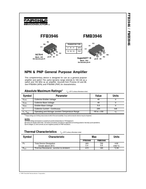
FFB3946中文资料
ON CHARACTERISTICS
hFE DC Current Gain IC = 100 µA, VCE = 1.0 V IC = 1.0 mA, VCE = 1.0 V IC = 10 mA, VCE = 1.0 V IC = 50 mA, VCE = 1.0 V IC = 100mA, VCE = 1.0 V IC = 10 mA, IB = 1.0 mA IC = 10 mA, IB = 1.0 mA 40 70 100 60 30 300
ACEx™ Bottomless™ CoolFET™ CROSSVOLT™ DOME™ E2CMOSTM EnSignaTM FACT™ FACT Quiet Series™ FAST
DISCLAIMER
FASTr™ GlobalOptoisolator™ GTO™ HiSeC™ ISOPLANAR™ MICROWIRE™ OPTOLOGIC™ OPTOPLANAR™ PACMAN™ POP™
Thermal Characteristics
Symbol
PD RθJA
TA = 25°C unless otherwise noted
Characteristic
Total Device Dissipation Derate above 25°C Thermal Resistance, Junction to Ambient FFB3946 300 2.4 415
TA = 25°C unless otherwise noted
Parameter
Value
40 40 5.0 200 -55 to +150
Units
V V V mA °C
4
Operating and Storage Junction Temperature Range
NST3904DP6T5G;中文规格书,Datasheet资料
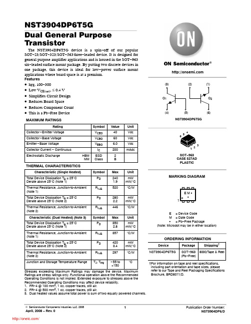
NST3904DP6T5GDual General Purpose TransistorThe NST3904DP6T5G device is a spin−off of our popular SOT−23/SOT−323/SOT−563 three−leaded device. It is designed for general purpose amplifier applications and is housed in the SOT−963 six−leaded surface mount package. By putting two discrete devices in one package, this device is ideal for low−power surface mount applications where board space is at a premium.Features•h FE, 100−300•Low V CE(sat), ≤ 0.4 V•Simplifies Circuit Design•Reduces Board Space•Reduces Component Count•This is a Pb−Free DeviceMAXIMUM RATINGSRating Symbol Value Unit Collector−Emitter Voltage V CEO40Vdc Collector−Base Voltage V CBO60Vdc Emitter−Base Voltage V EBO 6.0Vdc Collector Current − Continuous I C200mAdcElectrostatic Discharge HBMMM ESDClass2BTHERMAL CHARACTERISTICSCharacteristic (Single Heated)Symbol Max UnitTotal Device Dissipation T A = 25°C Derate above 25°C (Note 1)P D2401.9mWmW/°CThermal Resistance, Junction-to-Ambient (Note 1)R q JA520°C/WTotal Device Dissipation T A = 25°C Derate above 25°C (Note 2)P D2802.2mWmW/°CThermal Resistance, Junction-to-Ambient(Note 2)R q JA446°C/W Characteristic (Dual Heated) (Note 3)Symbol Max UnitTotal Device Dissipation T A = 25°C Derate above 25°C (Note 1)P D3502.8mWmW/°CThermal Resistance, Junction-to-Ambient(Note 1)R q JA357°C/WTotal Device Dissipation T A = 25°C Derate above 25°C (Note 2)P D4203.4mWmW/°CThermal Resistance, Junction-to-Ambient(Note 2)R q JA297°C/WJunction and Storage Temperature Range T J, T stg−55 to+150°CStresses exceeding Maximum Ratings may damage the device. Maximum Ratings are stress ratings only. Functional operation above the Recommended Operating Conditions is not implied. Extended exposure to stresses above the Recommended Operating Conditions may affect device reliability.1.FR−4 @ 100 mm2, 1 oz. copper traces, still air.2.FR−4 @ 500 mm2, 1 oz. copper traces, still air.3.Dual heated values assume total power is sum of two equally powered channels.SOT−963CASE 527ADPLASTICQ(3)2NST3904DP6T5GORDERING INFORMATIONMARKING DIAGRAMDevice Package Shipping†NST3904DP6T5G SOT−963(Pb−Free)8000/T ape & ReelE= Device CodeM= Date CodeG= Pb−Free PackageE M GG1†For information on tape and reel specifications, including part orientation and tape sizes, please refer to our T ape and Reel Packaging Specifications Brochure, BRD8011/D.(Note: Microdot may be in either location)3ELECTRICAL CHARACTERISTICS (T A = 25°C unless otherwise noted)CharacteristicSymbolMinMaxUnitOFF CHARACTERISTICSCollector −Emitter Breakdown Voltage (Note 4) (I C = 1.0 mAdc, I B = 0)V (BR)CEO 40−Vdc Collector −Base Breakdown Voltage (I C = 10 m Adc, I E = 0)V (BR)CBO 60−Vdc Emitter −Base Breakdown Voltage (I E = 10 m Adc, I C = 0)V (BR)EBO 6.0−Vdc Collector Cutoff Current (V CE = 30 Vdc, V EB = 3.0 Vdc)I CEX−50nAdcON CHARACTERISTICS (Note 4)DC Current Gain(I C = 0.1 mAdc, V CE = 1.0 Vdc)(I C = 1.0 mAdc, V CE = 1.0 Vdc)(I C = 10 mAdc, V CE = 1.0 Vdc)(I C = 50 mAdc, V CE = 1.0 Vdc)(I C = 100 mAdc, V CE = 1.0 Vdc)h FE40701006030−−300−−−Collector −Emitter Saturation Voltage (I C = 10 mAdc, I B = 1.0 mAdc)(I C = 50 mAdc, I B = 5.0 mAdc)V CE(sat)−−0.20.3VdcBase −Emitter Saturation Voltage (I C = 10 mAdc, I B = 1.0 mAdc)(I C = 50 mAdc, I B = 5.0 mAdc)V BE(sat)0.65−0.850.95VdcSMALL −SIGNAL CHARACTERISTICSCurrent −Gain − Bandwidth Product (I C = 10 mAdc, V CE = 20 Vdc, f = 100 MHz)f T 200−MHz Output Capacitance (V CB = 5.0 Vdc, I E = 0, f = 1.0 MHz)C obo − 4.0pF Input Capacitance (V EB = 0.5 Vdc, I C = 0, f = 1.0 MHz)C ibo −8.0pF Noise Figure (V CE = 5.0 Vdc, I C = 100 m Adc, R S = 1.0 k W , f = 1.0 kHz)NF−5.0dBSWITCHING CHARACTERISTICS Delay Time (V CC = 3.0 Vdc, V BE = −0.5 Vdc)t d −35nsRise Time (I C = 10 mAdc, I B1 = 1.0 mAdc)t r −35Storage Time (V CC = 3.0 Vdc, I C = 10 mAdc)t s −275nsFall Time(I B1 = I B2 = 1.0 mAdc)t f−504.Pulse Test: Pulse Width ≤300 m s; Duty Cycle ≤2.0%.I C , COLLECTOR CURRENT (A)Figure 1. Collector Emitter Saturation Voltage vs.Collector CurrentFigure 2. DC Current Gain vs. Collector CurrentI C , COLLECTOR CURRENT (A)V C E (s a t ), C O L L E C T O R −E M I T T E R S A T U R A T I O N V O L T A G E (V )h F E , D C C U R R E N T G A I N (V )Figure 3. Base Emitter Saturation Voltage vs.Collector CurrentFigure 4. Base Emitter Turn −On Voltage vs.Collector CurrentI C , COLLECTOR CURRENT (A)I C , COLLECTOR CURRENT (A)Figure 5. Saturation RegionFigure 6. Input CapacitanceI b , BASE CURRENT (A)V eb , EMITTER BASE VOLTAGE (V)Figure 7. Output CapacitanceV cb , COLLECTOR BASE VOLTAGE (V)V B E (s a t ), B A S E −E M I T T E R S A T U R A T I O N V O L T A G E (V )V B E (o n ), B A S E −E M I T T E R T U R N −O N V O L T A G E (V )V C E (s a t ), C O L L E C T O R −E M I T T E R S A T U R A T I O N V O L T A G E (V )C i b o , I N P U T C A P A C I T A N C E (p F )C o b o , O U T P U T C A P A C I T A N C E (p F )PACKAGE DIMENSIONSSOT −963CASE 527AD −01ISSUE B*For additional information on our Pb −Free strategy and solderingdetails, please download the ON Semiconductor Soldering and Mounting Techniques Reference Manual, SOLDERRM/D.SOLDERING FOOTPRINT*DIM MIN NOM MAX MILLIMETERS A 0.340.370.40b 0.100.150.20C 0.070.120.17D 0.95 1.00 1.05E 0.750.800.85e 0.35 BSC L 0.050.100.150.95 1.00 1.05H E0.0040.0060.0080.0030.0050.0070.0370.0390.0410.030.0320.0340.014 BSC0.0020.0040.0060.0370.0390.041MIN NOM MAXINCHES NOTES:1.DIMENSIONING AND TOLERANCING PER ANSI Y14.5M, 1982.2.CONTROLLING DIMENSION: MILLIMETERS3.MAXIMUM LEAD THICKNESS INCLUDES LEAD FINISH THICKNESS. MINIMUM LEAD THICKNESS IS THE MINIMUM THICKNESS OF BASE MATERIAL.ǒmm ǓON Semiconductor and are registered trademarks of Semiconductor Components Industries, LLC (SCILLC). SCILLC reserves the right to make changes without further notice to any products herein. SCILLC makes no warranty, representation or guarantee regarding the suitability of its products for any particular purpose, nor does SCILLC assume any liability arising out of the application or use of any product or circuit, and specifically disclaims any and all liability, including without limitation special, consequential or incidental damages.“Typical” parameters which may be provided in SCILLC data sheets and/or specifications can and do vary in different applications and actual performance may vary over time. All operating parameters, including “Typicals” must be validated for each customer application by customer’s technical experts. SCILLC does not convey any license under its patent rights nor the rights of others. SCILLC products are not designed, intended, or authorized for use as components in systems intended for surgical implant into the body, or other applications intended to support or sustain life, or for any other application in which the failure of the SCILLC product could create a situation where personal injury or death may occur. Should Buyer purchase or use SCILLC products for any such unintended or unauthorized application, Buyer shall indemnify and hold SCILLC and its officers, employees, subsidiaries, affiliates,and distributors harmless against all claims, costs, damages, and expenses, and reasonable attorney fees arising out of, directly or indirectly, any claim of personal injury or death associated with such unintended or unauthorized use, even if such claim alleges that SCILLC was negligent regarding the design or manufacture of the part. SCILLC is an Equal Opportunity/Affirmative Action Employer. This literature is subject to all applicable copyright laws and is not for resale in any manner.PUBLICATION ORDERING INFORMATION分销商库存信息: ONSEMINST3904DP6T5G。
NST3906DP6T5G;中文规格书,Datasheet资料
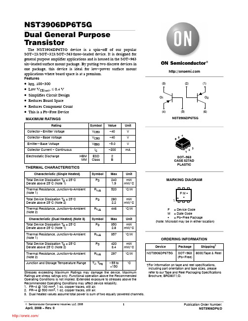
NST3906DP6T5GDual General Purpose TransistorThe NST3906DP6T5G device is a spin−off of our popular SOT−23/SOT−323/SOT−563 three−leaded device. It is designed for general purpose amplifier applications and is housed in the SOT−963 six−leaded surface mount package. By putting two discrete devices in one package, this device is ideal for low−power surface mount applications where board space is at a premium.Features•h FE, 100−300•Low V CE(sat), ≤ 0.4 V•Simplifies Circuit Design•Reduces Board Space•Reduces Component Count•This is a Pb−Free DeviceMAXIMUM RATINGSRating Symbol Value Unit Collector−Emitter Voltage V CEO−40V Collector−Base Voltage V CBO−40V Emitter−Base Voltage V EBO−5.0V Collector Current − Continuous I C−200mAElectrostatic Discharge HBMMM ESDClass2BTHERMAL CHARACTERISTICSCharacteristic (Single Heated)Symbol Max UnitTotal Device Dissipation T A = 25°C Derate above 25°C (Note 1)P D2401.9mWmW/°CThermal Resistance, Junction-to-Ambient (Note 1)R qJA520°C/WTotal Device Dissipation T A = 25°C Derate above 25°C (Note 2)P D2802.2mWmW/°CThermal Resistance, Junction-to-Ambient(Note 2)R q JA446°C/W Characteristic (Dual Heated) (Note 3)Symbol Max UnitTotal Device Dissipation T A = 25°C Derate above 25°C (Note 1)P D3502.8mWmW/°CThermal Resistance, Junction-to-Ambient(Note 1)R q JA357°C/WTotal Device Dissipation T A = 25°C Derate above 25°C (Note 2)P D4203.4mWmW/°CThermal Resistance, Junction-to-Ambient(Note 2)R q JA297°C/WJunction and Storage Temperature Range T J, T stg−55 to+150°CStresses exceeding Maximum Ratings may damage the device. Maximum Ratings are stress ratings only. Functional operation above the Recommended Operating Conditions is not implied. Extended exposure to stresses above the Recommended Operating Conditions may affect device reliability.1.FR−4 @ 100 mm2, 1 oz. copper traces, still air.2.FR−4 @ 500 mm2, 1 oz. copper traces, still air.3.Dual heated values assume total power is sum of two equally powered channels.Q(3)2NST3906DP6T5GORDERING INFORMATIONMARKING DIAGRAMDevice Package Shipping†NST3906DP6T5G SOT−963(Pb−Free)8000/T ape & Reel†For information on tape and reel specifications, including part orientation and tape sizes, please refer to our T ape and Reel Packaging Specifications Brochure, BRD8011/D.SOT−963CASE 527ADPLASTIC3F M GG1F= Device CodeM= Date CodeG= Pb−Free Package(Note: Microdot may be in either location)ELECTRICAL CHARACTERISTICS (T A = 25°C unless otherwise noted)CharacteristicSymbolMinMaxUnitOFF CHARACTERISTICSCollector −Emitter Breakdown Voltage (Note 4) (I C = 1.0 mAdc, I B = 0)V (BR)CEO −40−V Collector −Base Breakdown Voltage (I C = 10 m Adc, I E = 0)V (BR)CBO −40−V Emitter −Base Breakdown Voltage (I E = 10 m Adc, I C = 0)V (BR)EBO −5.0−V Collector Cutoff Current (V CE = 30 Vdc, V EB = 3.0 Vdc)I CEX−−50nAON CHARACTERISTICS (Note 4)DC Current Gain(I C = −0.1 mA, V CE = −1.0 V)(I C = −1.0 mA, V CE = −1.0 V)(I C = −10 mA, V CE = −1.0 V)(I C = −50 mA, V CE = −1.0 V)(I C = −100 mA, V CE = −1.0 V)h FE60801006030−−300−−−Collector −Emitter Saturation Voltage (I C = −10 mA, I B = −1.0 mA)(I C = −50 mA, I B = −5.0 mA)V CE(sat)−−−0.25−0.4VBase −Emitter Saturation Voltage (I C = −10 mA, I B = −1.0 mA)(I C = −50 mA, I B = −5.0 mA)V BE(sat)−0.65−−0.85−0.95VSMALL −SIGNAL CHARACTERISTICSCurrent −Gain − Bandwidth Product (I C = 10 mAdc, V CE = 20 Vdc, f = 100 MHz)f T 250−MHz Output Capacitance (V CB = −5.0 V, I E = 0 mA, f = 1.0 MHz)C obo − 4.5pF Input Capacitance (V EB = −0.5 V, I E = 0 mA, f = 1.0 MHz)C ibo −10.0pF Noise Figure (V CE = −5.0 V, I C = −100 m A, R S = 1.0 k Ω, f = 1.0 kHz)NF−4.0dBSWITCHING CHARACTERISTICSDelay Time (V CC = −3.0 V, V BE = 0.5 V)t d −35nsRise Time (I C = −10 mA, I B1 = −1.0 mA)t r −35Storage Time (V CC = −3.0 V, I C = −10 mA)t s −250nsFall Time(I B1 = I B2 = −1.0 mA)t f−504.Pulse Test: Pulse Width ≤300 μs; Duty Cycle ≤2.0%.I C , COLLECTOR CURRENT (A)Figure 1. Collector Emitter Saturation Voltage vs.Collector CurrentFigure 2. DC Current Gain vs. Collector CurrentI C , COLLECTOR CURRENT (A)V C E (s a t ), C O L L E C T O R −E M I T T E R S A T U R A T I O N V O L T A G E (V )h F E , D C C U R R E N T G A I N (V )Figure 3. Base Emitter Saturation Voltage vs.Collector CurrentFigure 4. Base Emitter Turn −On Voltage vs.Collector CurrentI C , COLLECTOR CURRENT (A)I C , COLLECTOR CURRENT (A)Figure 5. Saturation RegionFigure 6. Input CapacitanceI b , BASE CURRENT (A)V eb , EMITTER BASE VOLTAGE (V)Figure 7. Output CapacitanceV cb , COLLECTOR BASE VOLTAGE (V)V B E (s a t ), B A S E −E M I T T E R S A T U R A T I O N V O L T A G E (V )V B E (o n ), B A S E −E M I T T E R T U R N −O N V O L T A G E (V )V C E (s a t ), C O L L E C T O R −E M I T T E R S A T U R A T I O N V O L T A G E (V )C i b o , I N P U T C A P A C I T A N C E (p F )C o b o , O U T P U T C A P A C I T A N C E (p F )PACKAGE DIMENSIONSSOT −963CASE 527AD −01ISSUE B*For additional information on our Pb −Free strategy and solderingdetails, please download the ON Semiconductor Soldering and Mounting Techniques Reference Manual, SOLDERRM/D.SOLDERING FOOTPRINT*DIM MIN NOM MAX MILLIMETERS A 0.340.370.40b 0.100.150.20C 0.070.120.17D 0.95 1.00 1.05E 0.750.800.85e 0.35 BSC L 0.050.100.150.95 1.00 1.05H E0.0040.0060.0080.0030.0050.0070.0370.0390.0410.030.0320.0340.014 BSC0.0020.0040.0060.0370.0390.041MIN NOM MAXINCHES NOTES:1.DIMENSIONING AND TOLERANCING PER ANSI Y14.5M, 1982.2.CONTROLLING DIMENSION: MILLIMETERS3.MAXIMUM LEAD THICKNESS INCLUDES LEAD FINISH THICKNESS. MINIMUM LEAD THICKNESS IS THE MINIMUM THICKNESS OF BASE MATERIAL.ǒmm inchesǓSCALE 20:1ON Semiconductor and are registered trademarks of Semiconductor Components Industries, LLC (SCILLC). SCILLC reserves the right to make changes without further notice to any products herein. SCILLC makes no warranty, representation or guarantee regarding the suitability of its products for any particular purpose, nor does SCILLC assume any liability arising out of the application or use of any product or circuit, and specifically disclaims any and all liability, including without limitation special, consequential or incidental damages.“Typical” parameters which may be provided in SCILLC data sheets and/or specifications can and do vary in different applications and actual performance may vary over time. All operating parameters, including “Typicals” must be validated for each customer application by customer’s technical experts. SCILLC does not convey any license under its patent rights nor the rights of others. SCILLC products are not designed, intended, or authorized for use as components in systems intended for surgical implant into the body, or other applications intended to support or sustain life, or for any other application in which the failure of the SCILLC product could create a situation where personal injury or death may occur. Should Buyer purchase or use SCILLC products for any such unintended or unauthorized application, Buyer shall indemnify and hold SCILLC and its officers, employees, subsidiaries, affiliates,and distributors harmless against all claims, costs, damages, and expenses, and reasonable attorney fees arising out of, directly or indirectly, any claim of personal injury or death associated with such unintended or unauthorized use, even if such claim alleges that SCILLC was negligent regarding the design or manufacture of the part. SCILLC is an Equal Opportunity/Affirmative Action Employer. This literature is subject to all applicable copyright laws and is not for resale in any manner.PUBLICATION ORDERING INFORMATION分销商库存信息: ONSEMINST3906DP6T5G。
39426-0005中文资料
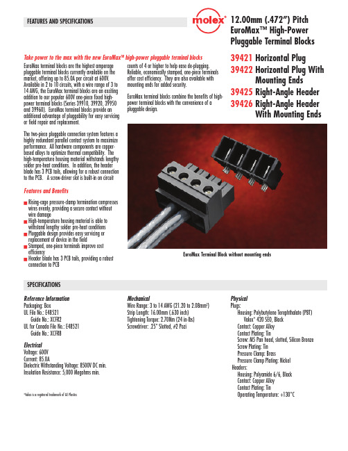
FEATURES AND SPECIFICATIONSSPECIFICATIONS 12.00mm (.472”) Pitch EuroMax™ High-Power Pluggable Terminal Blocks 39421 Horizontal Plug39422Horizontal Plug WithMounting Ends 39425Right-Angle Header 39426 Right-Angle HeaderWith Mounting EndsEuroMax terminal blocks are the highest amperage pluggable terminal blocks currently available on the market, offering up to 85.0A per circuit at 600V.Available in 2 to 10 circuits, with a wire range of 3 to 14 AWG, the EuroMax terminal blocks are an excitingaddition to our popular 600V one-piece fixed high-power terminal blocks (Series 39910, 39920, 39950and 39960). EuroMax terminal blocks provide anadditional advantage of pluggability for easy servicing or field repair and replacement.The two-piece pluggable connection system features a highly redundant parallel contact system to maximize performance. All hardware components are copper-based alloys to optimize thermal compatibility. The high-temperature housing material withstands lengthy solder pre-heat conditions. In addition, the header blade has 3 PCB tails, allowing for a robust connection to the PCB. A screw-driver slot is built-in on circuit counts of 4 or higher to help ease de-plugging.Reliable, economically stamped, one-piece terminals offer cost efficiency. They are also available with mounting ends for added security. EuroMax terminal blocks combine the benefits of high-power terminal blocks with the convenience of a pluggable design. Reference Information Packaging: Box UL File No.: E48521Guide No.: XCFR2UL for Canada File No.: E48521Guide No.: XCFR8Electrical Voltage: 600V Current: 85.0ADielectric Withstanding Voltage: 8500V DC min.Insulation Resistance: 5,000 Megohms min.MechanicalWire Range: 3 to 14 AWG (21.20 to 2.08mm 2)Strip Length: 16.00mm (.630 inch)Tightening Torque: 2.70Nm (24 in-lbs)Screwdriver: .25” Slotted, #2 PoziPhysical Plugs:Housing: Polybutylene Terephthalate (PBT)Valox* 420 SEO, Black Contact: Copper Alloy Contact Plating: TinScrew: M5 Pan head, slotted, Silicon Bronze Screw Plating: Tin Pressure Clamp: BrassPressure Clamp Plating: Nickel Headers:Housing: Polyamide 6/6, Black Contact: Copper Alloy Contact Plating: TinOperating Temperature: +130°CFeatures and BenefitsI Rising-cage pressure-clamp termination compresseswires evenly, providing a secure contact without wire damageI High-temperature housing material is able to withstand lengthy solder pre-heat conditions I Pluggable design provides easy servicing or replacement of device in the fieldI Stamped, one-piece terminals improve cost efficiencyI Header blade has 3 PCB tails, providing a robust connection to PCBTake power to the max with the new EuroMax TM high-power pluggable terminal blocks EuroMax Terminal Block without mounting ends*Valox is a registered trademark of GE PlasticsM4 MountingScrewsM4 ThreadedInsertsHeader BladeTerminalHeader BodyPlug BodyTerminal withBack PlateM5 ScrewPressureClampCapAPPLICATIONS12.00mm (.472”) PitchEuroMax™ High-PowerPluggable Terminal BlocksI Motors and drivesI Power controls and convertersI Process controlsI InvertorsI Distributed power systemsI Cellular base stationsI Load control systemsI Solar power systemsI Fuel cellsAmericas HeadquartersLisle, Illinois 60532 U.S.A.1-800-78MOLEXamerinfo@Far East North HeadquartersYamato, Kanagawa, Japan81-462-65-2324feninfo@Far East South HeadquartersJurong, Singapore65-6-268-6868fesinfo@European HeadquartersMunich, Germany49-89-413092-0eurinfo@Corporate Headquarters2222 Wellington Ct.Lisle, IL 60532 U.S.A.630-969-4550Fax:630-969-1352Visit our Web site at /product/tblocks/euromax.htmlOrder No. USA-304Printed in USA/2.5K/JI/JI/2005.04©2005 Molex ORDERING INFORMATIONCircuitsOrder No.Horizontal Plug Right-Angle HeaderWithout Mounting Ends With Mounting Ends Without Mounting Ends With Mounting Ends 239421-000239422-000239425-000239426-0002339421-000339422-000339425-000339426-0003439421-000439422-000439425-000439426-0004539421-000539422-000539425-000539426-0005639421-000639422-000639425-000639426-0006739421-000739422-000739425-000739426-0007839421-000839422-000839425-000839426-0008939421-0009—39425-0009—1039421-001039425-0010Horizontal PlugSeries 39421Horizontal Plug with Mounting EndsSeries 39422Right-Angle HeaderSeries 39425Right-Angle Header with Mounting EndsSeries 39426。
B3942 data sheet(revise)MOS管规格书
B3942N- and P-Channel 30-V (D-S) MOSFETVersion: 0.01Please read the notice stated in this preamble carefully before accessing any contents of the document attached.Admission of BiTEK’s statement therein is presumed once the document is released to the receiver.Notice:Firstly, the information furnished by Beyond Innovation Technology Co. Ltd. (BiTEK) in this document is believed to be accurate and reliable and subject to BiTEK’s amendment without prior notice. And the aforesaid information does not form any part or parts of any quotation or contract between BiTEK and the information receiver.Further, no responsibility is assumed for the usage of the aforesaid information. BiTEK makes no representation that the interconnect of its circuits as described herein will not infringe on exiting or future patent rights, nor do the descriptions contained herein imply the granting of licenses to make, use or sell equipment constructed in accordance therewith.Besides, the product in this document is not designed for use in life support appliances, devices, or systems where malfunction of this product can reasonably be expected to result in personal injury. BiTEK customers’ using or selling this product for use in such applications shall do so at their own risk and agree to fully indemnify BiTEK for any damage resulting from such improper use or sale.At last, the information furnished in this document is the property of BiTEK and shall be treated as highly confidentiality; any kind of distribution, disclosure, copying, transformation or use of whole or parts of this document without duly authorization from BiTEK by prior written consent is strictly prohibited. The receiver shall fully compensate BiTEK without any reservation for any losses thereof due to its violation of BiTEK’s confidential request. The receiver is deemed to agree on BiTEK’s confidential request therein suppose that said receiver receives this document without making any expressly opposition. In the condition that aforesaid opposition is made, the receiver shall return this document to BiTEK immediately without any delay. -Version A4。
A3941KLPTR-T;中文规格书,Datasheet资料
1.508.853.5000;
A3941
Automotive Full Bridge MOSFET Driver
ELECTRICAL CHARACTERISTICS valid at TJ = –40°C to 150°C, VBB = 7 to 50 V, unless noted otherwise
IBBQ IBBS
VREG
RESET = high, outputs = low, VBB = 12 V
–
10
14
RESET = low, Sleep mode, VBB = 12 V
–
–
10
VBB > 9 V, IREG = 0 to 10 mA
12.5
13
13.75
7.5 V < VBB ≤ 9 V, IREG = 0 to 7 mA
Integrated diagnostics provide indication of undervoltage, overtemperature, and power bridge faults, and can be configured to protect the power MOSFETs under most short circuit conditions.
Characteristics
Symbol
Test Conditions
Min. Typ. Max.
Supply and Reference
Load Supply Voltage Functional Operating Range1
VBB
5.5
–
50
Load Supply Quiescent Current VREG Output Voltage
华北 NORCO EMB-3940 说明书
EMB-3940说明书V1.1说明除列明随产品配置的配件外,本手册包含的内容并不代表本公司的承诺,本公司保留对此手册更改的权利,且不另行通知。
对于任何因安装、使用不当而导致的直接、间接、有意或无意的损坏及隐患概不负责。
订购产品前,请向经销商详细了解产品性能是否符合您的需求。
NORCO 是深圳华北工控有限公司的注册商标。
本手册所涉及到的其他商标,其所有权为相应的产品厂家所拥有。
本手册内容受版权保护,版权所有。
未经许可,不得以机械的、电子的或其它任何方式进行复制。
温馨提示1.产品使用前,务必仔细阅读产品说明书。
2.对未准备安装的板卡,应将其保存在防静电保护袋中。
3.在从包装袋中拿板卡前,应将手先置于接地金属物体上一会儿,以释放身体及手中的静电。
4.在拿板卡时,需佩戴静电保护手套,并且应该养成只触及其边缘部分的习惯。
5.主板与电源连接时,请确认电源电压。
6.为避免人体被电击或产品被损坏,在每次对主板、板卡进行拔插或重新配置时,须先关闭交流电源或将交流电源线从电源插座中拔掉。
7.在对板卡进行搬动前,先将交流电源线从电源插座中拔掉。
8.当您需连接或拔除任何设备前,须确定所有的电源线事先已被拔掉。
9.为避免频繁开关机对产品造成不必要的损伤,关机后,应至少等待30秒后再开机。
10.设备在使用过程中出现异常情况,请找专业人员处理。
11.此为A级产品,在生活环境中,该产品可能会造成无线电干扰。
在这种情况下,可能需要用户对其干扰采取切实可行的措施。
目录第一章产品介绍 (3)1.1 简介 (3)1.2 产品规格 (3)第二章安装说明 (3)2.1 接口位置和尺寸图 (3)2.2 安装步骤 (3)2.3 内存安装 (4)2.4 跳线功能设置 (4)2.4.1CMOS内容清除/保持设置(JCC) (4)2.4.2 硬件来电开机插针(JAT) (5)2.4.3 COM2 跳线功能设置(J1,J2,J3) (6)2.5 接口说明 (6)2.5.1SATA接口(SATA、PWR_OUT) (6)2.5.2 串行接口(COM1-2,COM3-6) (7)2.5.3 显示接口(VGA、LVDS、DP) (9)2.5.4 LVDS电压及背光设置接口(LVDS_BKLT、JLVDS) (11)2.5.5USB接口(USB30、USB34、USB56、USB78) (11)2.5.6网络接口(LAN1,LAN2) (13)2.5.7 音频接口(AUDIO) (14)2.5.8音频功放接口(AMP) (14)2.5.9 可编程输入输出口(GPIO) (15)2.5.10 键盘鼠标接口(KBMS) (16)2.5.11 电源接口(PWR) (16)2.5.12 前面板接口(JFP) (17)2.5.13 内存插槽(SO-DIMM) (18)2.5.14 扩展接口(MINI_ PCIE1、MINI_ PCIE2) (18)第三章BIOS程序设置 (25)AMI BIOS刷新 (25)AMI BIOS描述 (25)BIOS参数设置 (25)3.1 Main菜单 (26)3.2 Advanced (27)3.2.1 ACPI Settings (28)3.2.2 F81866 Supper IO Configuration (29)3.2.3Hardware Monitor (31)3.2.4 APM Configuration (32)3.2.5 Serial Port Console Redirection (33)3.2.6 CPU Configuration (34)3.2.7 PPM Configuration (36)3.2.8SATA Configuration (37)3.2.9 LPSS & SCC Configuration (38)3.2.10 System Configuration (39)3.2.11 Network Stack Configuration (40)3.2.12 CSM Configuration (41)3.2.13 SDIO Configuration (42)3.2.14USB Configuration (43)3.3 Chipset菜单 (44)3.3.1North Bridge (45)3.3.2South Bridge (46)3.4 Boot菜单 (47)3.5 Security 菜单 (48)3.6 Save&Exit菜单 (49)附录 (52)附一:Watchdog 编程指引 (52)附二:IRQ和System Memory Map,1st MB Memory Map (54)附三:术语表 (56)第一章产品介绍1.1 简介EMB-3940采用Intel Braswell芯片组,板载N3060/N3160处理器;1条单通道SO_DIMM 插槽,支持DDR3L 1066/1333/1600,内存容量最高可达8GB。
MAXIM MAX3946评估板 说明书
MAX3946评估板_________________________________________________________________Maxim Integrated Products __1本文是英文数据资料的译文,文中可能存在翻译上的不准确或错误。
如需进一步确认,请在您的设计中参考英文资料。
有关价格、供货及订购信息,请联络Maxim 亚洲销售中心:10800 852 1249 (北中国区),10800 152 1249 (南中国区),或访问Maxim 的中文网站: 。
评估板: MAX3946概述MAX3946评估板(EV kit)是完全安装的演示板,为1.0625Gbps 至11.3Gbps 激光驱动器MAX3946提供光学评估。
控制软件通过USB 口与评估板通信,并提供对所有器件功能的简便控制。
评估板可完全由USB 口供电,用户也可以选择外部3.3V 单电源为器件供电,而USB 口为板载微控制器供电。
评估板上的柔性电缆允许连接带柔性电缆的激光器。
评估板内容♦♦MAX3946评估电路板特性♦♦驱动差分连接激光器♦♦软件控制MAX3946♦♦通过USB 或外部电源供电器件列表19-5755; Rev 0; 2/11定购信息*EP = 裸焊盘。
PARTTYPE MAX3946EVKITEV KitDESIGNATION QTY DESCRIPTIONC1–C6, C8, C9,C16, C41100.01F F Q 10% ceramic capacitors (0402)C7, C10, C12,C1440.1F F Q 20% ceramic capacitors (0204)C11, C13, C15310F F Q 10% ceramic capacitors (0805)C17–C200Not installedC21, C22233pF Q 10% ceramic capacitors (0402)C25, C26, C27, C49, C5250.1F F Q 10% ceramic capacitors (0402)C34, C5521F F Q 10% ceramic capacitors (0603)C35, C37, C383 4.7F F Q 10% ceramic capacitors (0805)D61Green LEDJ1, J22SMA edge-mount connectors J3, J4, TP3, TP7, TP10–TP138Test points J81USB connectorJU21 2 x 6 header, 0.1in centers L1122F H Q 20% inductorTaiyo Yuden CBC3225T220M L2, L3218nH Q 2% inductors (0402)L4, L11, L123Ferrite beads (0402)Murata BLM15GG471DESIGNATION QTY DESCRIPTIONL10, L14, L15, L16410F H Q 10% inductors (0603)R1, R22 1.00k I Q 1% resistors (0402)R31680I Q 5% resistor (0402)R5, R6220I Q 5% resistors (0603)R7, R82100I Q 5% resistors (0603)R15, R502 4.7k I Q 5% resistors (0402)R16, R1721k I Q 5% resistors (0402)R18, R52, R55, R66, R73551I Q 5% resistors (0402)R241 1.5k I Q 5% resistor (0402)R31, R51, R53310k I Q 5% resistors (0402)SW11SPDT switchU111.0625Gbps to 11.3Gbps, SFP+ laser driver (24 TQFN-EP*)Maxim MAX3946ETG+ U21Low-noise LDO regulator (8 TDFN-EP*)Maxim MAX8902AATA+ U60User-supplied TOSA U101Microcontroller (28 SO)Microchip PIC16C745-I/SO Y216MHz crystalECS Inc. ECS-60-32-5PXDN —1PCB: MAX3946 EVALUATION BOARD, REV AMAX3946评估板评估板: M A X 39462_________________________________________________________________________________________快速入门注:下文中,与软件相关的内容用粗体字表示,粗体内容表示直接来自评估软件。
MMDT3946-7-F中文资料

MMDT3946COMPLEMENTARY NPN / PNP SMALL SIGNAL SURFACE MOUNT TRANSISTOR·Complementary Pair ·One 3904-Type NPN, One 3906-Type PNP·Epitaxial Planar Die Construction·Ideal for Low Power Amplification and Switching ·Ultra-Small Surface Mount Package ·Lead Free/RoHS Compliant (Note 3)FeaturesMaximum Ratings, NPN 3904 Section@ T A = 25°C unless otherwise specifiedMechanical Data·Case: SOT-363·Case Material: Molded Plastic. UL Flammability Classification Rating 94V-0·Moisture Sensitivity: Level 1 per J-STD-020C ·Terminals: Solderable per MIL-STD-202, Method 208·Lead Free Plating (Matte Tin Finish annealed over Alloy 42 leadframe).·Terminal Connections: See Diagram ·Marking (See Page 3): K46·Ordering & Date Code Information: See Page 3·Weight: 0.006 grams (approximate)Notes: 1. Device mounted on FR-4 PCB, 1 inch x 0.85 inch x 0.062 inch; pad layout as shown on Diodes Inc. suggested pad layout document AP02001, which can be found on our website at /datasheets/ap02001.pdf. 2. Maximum combined dissipation. 3. No purposefully added lead.E 1, B 1, C 1 = PNP3906 Section E 2, B 2, C 2 = NPN3904 SectionLead-freeElectrical Characteristics, NPN 3904 Section @ T A = 25°C unless otherwise specifiedNote: 4.Short duration pulse test used to minimize self-heating effect.Electrical Characteristics, PNP 3906 Section@ T A = 25°C unless otherwise specifiedDate Code Key K46 = Product Type Marking Code YM = Date Code Marking Y = Year ex: N = 2002M = Month ex: 9 = SeptemberMarking InformationOrdering Information(Note 5)Notes: 4. Short duration pulse test used to minimize self-heating effect.5. For Packaging Details, go to our website at /datasheets/ap02007.pdf.1100.11101001000V , B A S E -E M I T T E R B E (S A T )S A T U R A T I O N V O L T A G E (V )I , COLLECTOR CURRENT (mA)C Fig. 5, Typical Base-EmitterSaturation Voltage vs. Collector Current (NPN-3904)0.010.110.11101001000V , C O L L E C T O R -E M I T T E R C E (S A T )S A T U R A T I O N V O L T A G E (V )I , COLLECTOR CURRENT (mA)C Fig. 4, Typical Collector-EmitterSaturation Voltage vs. Collector Current (NPN-3904)11010001000.11101000100h , D C C U R R E N T G A I NF E I , COLLECTOR CURRENT (mA)C Fig. 3, Typical DC Current Gain vs Collector Current (NPN-3904)T = -25°CA T = +25°CA T = 125°CA V = 1.0VCE 0515100.1110100C , I N P U T C A P A C I T A N C E (p F )I B O C , O U T P U T C A P A C I T A N C E (p F )O B O V , COLLECTOR-BASE VOLTAGE (V)CB Fig. 2, Input and Output Capacitance vs.Collector-Base Voltage (NPN-3904)CiboCobof = 1MHz050100255075100125150175200P , P O W E R D I S S I P A T I O N (m W )D T , AMBIENT TEMPERATURE (°C)A Fig. 1, Max Power Dissipation vs Ambient Temperature (Total Device)1502002503003500100100.1110100C , I N P U T C A P A C I T A N C E (p F )I B O C , O U T P U T C A P A C I T A N C E (p F )O B O V , COLLECTOR-BASE VOLTAGE (V)CB Fig. 6, Input and Output Capacitance vs.Collector-Base Voltage (PNP-3906)0.50.60.70.80.91.0110100V , B A S E -E M I T T E R B E (S A T )S A T U R A T I O N V O L T A G E (V )I , COLLECTOR CURRENT (mA)C Fig. 9, Typical Base-EmitterSaturation Voltage vs. Collector Current (PNP-3906)0.010.11011101001000V , C O L L E C T O R -E M I T T E R C E (S A T )S A T U R A T I O N V O L T A G E (V )I , COLLECTOR CURRENT (mA)C Fig. 8, Typical Collector-Emitter Saturation Voltagevs. Collector Current (PNP-3906)I CI B = 1011010001000.11101000100h , D C C U R R E N T G A I NF E I , COLLECTOR CURRENT (mA)C Fig. 7, Typical DC Current Gain vsCollector Current (PNP-3906)T = -25°CA T = +25°CA T = 125°CA V = 1.0VCE IMPORTANT NOTICEDiodes Incorporated and its subsidiaries reserve the right to make modifications, enhancements, improvements, corrections or other changes without further notice to any product herein. Diodes Incorporated does not assume any liability arising out of the application or use of any product described herein; neither does it convey any license under its patent rights, nor the rights of others. The user of products in such applications shall assume all risks of such use and will agree to hold Diodes Incorporated and all the companies whose products are represented on our website, harmless against all damages.LIFE SUPPORTDiodes Incorporated products are not authorized for use as critical components in life support devices or systems without the expressed written approval of the President of Diodes Incorporated.。
OPPO-5G-CPE-T1 数据手册说明书
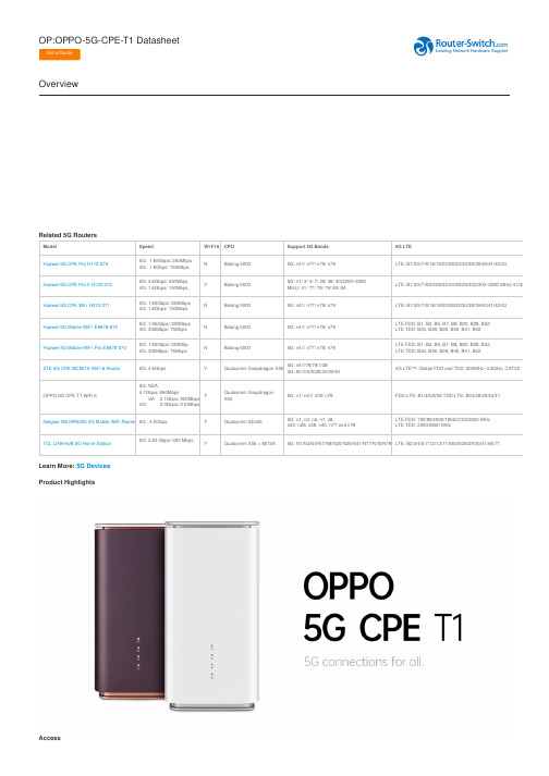
OP:OPPO-5G-CPE-T1 DatasheetOverviewRelated 5G RoutersModel Speed Wi-Fi 6CPU Support 5G Bands4G LTEHuawei 5G CPE Pro H112-3725G: 1.65Gbps/ 250Mbps4G : 1.6Gbps/ 150MbpsN Balong 50005G: n41/ n77/ n78/ n79LTE: B1/3/5/7/8/18/19/20/28/32/34/38/39/40/41/42/43Huawei 5G CPE Pro 2 H122-3735G: 3.6Gbps/ 250Mbps4G: 1.6Gbps/ 150MbpsY Balong 50005G: n1/ 3/ 5/ 7/ 28/ 38/ 40(2300–2390MHz)/ 41/ 77/ 78/ 79/ 80/ 84LTE: B1/3/5/7/8/20/28/32/34/38/39/40(2300–2390 MHz)/41/42/43Huawei 5G CPE Win H312-3715G: 1.65Gbps/ 250Mbps4G: 1.6Gbps/ 150MbpsN Balong 50005G: n41/ n77/ n78/ n79LTE: B1/3/5/7/8/18/19/20/28/32/34/38/39/40/41/42/43Huawei 5G Mobile WiFi E6878-8705G: 1.65Gbps/ 250Mbps4G: 300Mbps/ 75MbpsN Balong 50005G: n41/ n77/ n78/ n79LTE FDD: B1, B3, B5, B7, B8, B20, B28, B32LTE TDD: B34, B38, B39, B40, B41, B42Huawei 5G Mobile WiFi Pro E6878-3705G: 1.65Gbps/ 250Mbp4G: 300Mbps/ 75MbpsN Balong 50005G: n41/ n77/ n78/ n79LTE FDD: B1, B3, B5, B7, B8, B20, B28, B32LTE TDD: B34, B38, B39, B40, B41, B42ZTE 5G CPE MC801A WiFi 6 Router5G: 4.6Gbps Y Qualcomm Snapdragon X555G: n41/78/79/1/284G: B1/3/5/8/28/34/39/404G LTE™: Global FDD and TDD, 600MHz~3.8GHz, CAT22OPPO 5G CPE T1 WiFi 65G: NSA4.1Gbps/ 660MbpsSA 2.1Gbps/ 900Mbps4G: 2.0Gbps/ 210MbpsYQualcomm SnapdragonX555G: n1/ n41/ n78/ n79FDD-LTE: B1/3/5/8/28 TDD-LTE: B34/38/39/40/41Netgear M5 MR5200 5G Mobile WiFi Router5G : 4.0Gbps Y Qualcomm SDx555G: n1, n3, n5, n7, n8,n20, n28, n38, n40, n77 and n78LTE FDD: 700/800/900/1800/2100/2600 MHzLTE TDD: 2300/2600 MHzTCL LINKHUB 5G Home Station 5G: 2.83 Gbps/ 300 MbpsY Qualcomm X55 + 8072A5G: N1/N3/N5/N7/N8/N20/N28/N41/N77/N78/N79LTE: B2/3/4/5/7/12/13/17/48/25/26/29/30/41/66/71Learn More: 5G Devices Product HighlightsAccess5G Plug-in, Wi-Fi outNo longer limited to traditional fixed wired access. Once plugged-in and 5G SIM card inserted, T1 provides stable and high-speed Wi-Fi.AntennasO-Reserve 5G AntennasT1 is equipped with 8 built-in antennas for sub-6 GHz band. 4 best gain out of 8 will be chosen algorithmically to communicate with the base station by 4x4 MIMO, achieving 6.7dBi¹ antenna gain.ChipsetSnapdragon X55 ModemSnapdragon X55 supports SA/NSA, 5G/4G spectrum sharing and the full sub-6 GHz band, which enables T1 to meet what you need. 5.0Gbps² peak DL rate provides a fast network experience no matter connected to LAN or Wi-Fi.Wi-FiDual band Wi-Fi, 802.11axT1 boasts higher transmission rates and stronger performance. With 2.4GHz and 5GHz dual bands, its Wi-Fi downlink rate can reach 1.8Gbps³; it also features OFDMA, 2x2 MU MIMO and beamforming.One more way to connect.T1 is equipped with 3 GE ports as well, allowing a near 5G experience even throught wired access.That is, your most frequently used mobile and smart devices can all be connected.The seamless experience is just the most natural way to enjoy a smart lifestyle.O-Connect* - for multiple platforms and various scenarios.NOTE:* O-Connect is the software for using OPPO 5G CPE products, OPPO may update real-time adjustments to the software accordingly.Compare to Similar ItemsTable 1 shows the comparison.Product Code OPPO 5G CPE T1a OPPO 5G CPE T1 5G frequency band5G: n1/n28/n41/n78/n795G: n41/n78/n79 Storage512M RAM+512M ROM1G RAM+1G ROMInterface Gigabit LAN/WAN x1Gigabit LAN x1Gigabit LAN/WAN x1 Gigabit LAN x2USB\USB 2.0 x1External antenna\TS9 external antenna port x2 Software experience* The overall performance is optimized, and the measured overall rate ishigher.* Management page revision.1) Brand new page style2) Increase parental control function3) Compared with T1 removal function-signal scoring, PIN/PUK settings,terminal management (subsequent OTA upgrade support), flight modeswitchThe old versionConfigurationFollow this guide to configure OPPO 5G CPE T1.Get More InformationDo you have any question about the OPPO 5G CPE T1?Contact us now via Live Chat or ***********************.SpecificationOPPO 5G CPE T1 SpecificationModem Qualcomm Snapdragon X55 5G modemCPU ARM Cortex-A7 up to 1.5GHz5G4n1/ n41/ n78/ n79Antenna O-Reserve 5G Antennas (4x4 MIMO), antenna gain reachs 6.7dBi1MAIN, DIV extension portsWLAN IEEE802.11(a/b/g/n/ac/ax)2x2 MIMOUp to 1.8Gbps3 DL rateMU MIMOPorts and Buttons Power, Reset, WPSNano-SIM / eSIMUSB 3.0 *1GE LAN *2, GE WAN/LAN *1DC-INPUTPower AC 100~240V, 50/60Hz, DC 12V/2ADimensions and Weight92mm x 92mm x 180mmColor White, Brown1. The antenna gain is tested in OPPO's lab, the actual performance varies according to the environment and base station.2. Theorectical rate based on product design. The rate in use depends on the operator.3. Theorectical rate based on product design. The rate in use depends on the operator and the environment.4. OPPO 5G CPE T1 supports virtually any sub-6 GHz bands, and could be customized by operator's needs.Want to Buy200+Countries we Sold18,000+Customers Trusted$20,000,000Inventory Available50%-98%Off Global List Price100%Safe Online ShoppingWhy As a leading network hardware supplier, focuses on original new ICT equipment of Cisco , Huawei , HPE , Dell , Hikvision , Juniper , Fortinet , etc.Contact Us● Tel: +1-626-655-0998 (USA) +852-3050-1066 / +852-3174-6166● Fax: +852-3050-1066 (Hong Kong)● Email: ***********************。
3956;中文规格书,Datasheet资料

/
3956
AC axial compact fan
Product drawing
Web data sheet XI · Page 3 of 4 ebm-papst St. Georgen GmbH & Co. KG · Hermann-Papst-Straße 1 · D-78112 St. Georgen · Phone +49 7724 81-0 · Fax +49 7724 81-1309 · info2@ ·
Mass Dimensions Material of impeller Housing material Direction of air flow Direction of rotation Bearing Lifetime L10 at 40 °C Lifetime L10 at maximum temperature Connection line Motor protection Approval
ml = max. load · me = max. efficiency · fa = running at free air · cs = customer specs · cu = customer unit Subject to alterations
Web data sheet XI · Page 1 of 4 ebm-papst St. Georgen GmbH & Co. KG · Hermann-Papst-Straße 1 · D-78112 St. Georgen · Phone +49 7724 81-0 · Fax +49 7724 81-1309 · info2@ ·
/
3956
STTH8S06D;STTH8S06FP;中文规格书,Datasheet资料
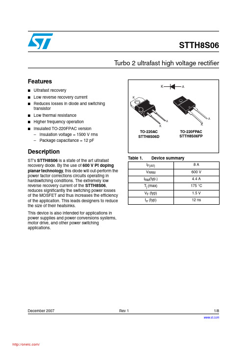
December 2007 Rev 11/8STTH8S06Turbo 2 ultrafast high voltage rectifierFeatures■Ultrafast recovery■Low reverse recovery current■Reduces losses in diode and switching transistor■Low thermal resistance ■Higher frequency operation ■Insulated TO-220FPAC version –Insulation voltage = 1500 V rms –Package capacitance = 12 pFDescriptionST's STTH8S06 is a state of the art ultrafast recovery diode. By the use of 600 V Pt doping planar technology , this diode will out-perform the power factor corrections circuits operating in hardswitching conditions. The extremely low reverse recovery current of the STTH8S06,reduces significantly the switching power losses of the MOSFET and thus increases the efficiency of the application. This leads designers to reduce the size of their heatsinks.This device is also intended for applications in power supplies and power conversions systems, motor drive, and other power switching applications.Table 1.Device summaryI F(AV)8 A V RRM 600 V I RM (typ.) 4.4 A T j (max)175 °C V F (typ) 1.5 V t rr (typ)12 nsCharacteristics STTH8S062/81 CharacteristicsTo evaluate the maximum conduction losses use the following equation:P = 1.20 x I F(AV) + 0.087 I F 2(RMS)Table 2.Absolute ratings (limiting values)Symbol ParameterValue Unit V RRM Repetitive peak reverse voltage 600V I F(AV)Average forward current8A I FSM Surge non repetitive forward current t p = 10 ms60A T stg Storage temperature range-65 to + 175°C T jMaximum operating junction temperature175°CTable 3.Thermal parameterSymbol ParameterMaximumUnit R th(j-c)Junction to caseTO-220AC 3.0°C/WTO220FP AC5.5Table 4.Static electrical characteristicsSymbol ParameterTest conditions Min.TypMax.Unit I RReverse leakage currentT j = 25 °C V R = 600 V20µAT j = 125 °C 25200V FForward voltage dropT j = 25 °C I F = 8 A3.4VT j = 125 °C1.51.9Table 5.Dynamic electrical characteristicsSymbol ParameterTest conditionsMin.Typ Max.Unit t rr Reverse recovery time I F = 1 A, dI F /dt = - 200 A/µs, V R = 30 V1218ns I RM Reverse current T j = 25 °CI F = 8 A, dI F /dt = - 200 A/µs, V R = 200 V 1.6 2.2A S factor Softness factor1-Q rr Reverse recovery charges 17nC I RM Reverse current T j = 125 °CI F = 8 A, dI F /dt = - 200 A/µs, V R = 200 V4.4 6.0A S factor Softness factor0.3-Q rrReverse recovery charges90nCSTTH8S06Characteristics3/8Figure 1.Forward voltage drop versus forward currentFigure 2.Relative variation of thermalimpedance junction to case versusFigure 3.Relative variation of thermal impedance junction to case versus Figure 4.Peak reverse recovery current versus dI F /dt (typical values)Tδ=tp/TtpCharacteristics STTH8S06 Figure 5.Reverse recovery time versus dI F/dt Figure 6.Reverse recovery charges versus4/8STTH8S06Package information5/82 Package information●Epoxy meets UL94, V0●Cooling method: by conduction (C)●Recommended torque value: 0.4 to 0.6 N·mIn order to meet environmental requirements, ST (also) offers these devices in ECOPACK®packages. ECOPACK® packages are Lead-free. The category of second level Interconnect is marked on the package and on the inner box label, in compliance with JEDEC Standard JESD97. The maximum ratings related to soldering conditions are also marked on the inner box label.ECOPACK is an ST trademark. ECOPACK specifications are available at: .Package information STTH8S066/8STTH8S06Ordering information7/83 Ordering information4 Revision historyTable 8.Ordering informationOrder code Marking Package Weight Base qtyDelivery modeSTTH8S06D STTH8S06D TO-220AC 1.9 g 50Tube STTH8S06FPSTTH8S06FPTO-220FP AC1.64 g50TubeTable 9.Document revision historyDate RevisionDescription of changes18-Dec-20071First issue.STTH8S068/8Please Read Carefully:Information in this document is provided solely in connection with ST products. STMicroelectronics NV and its subsidiaries (“ST”) reserve the right to make changes, corrections, modifications or improvements, to this document, and the products and services described herein at any time, without notice.All ST products are sold pursuant to ST’s terms and conditions of sale.Purchasers are solely responsible for the choice, selection and use of the ST products and services described herein, and ST assumes no liability whatsoever relating to the choice, selection or use of the ST products and services described herein.No license, express or implied, by estoppel or otherwise, to any intellectual property rights is granted under this document. If any part of this document refers to any third party products or services it shall not be deemed a license grant by ST for the use of such third party products or services, or any intellectual property contained therein or considered as a warranty covering the use in any manner whatsoever of such third party products or services or any intellectual property contained therein.UNLESS OTHERWISE SET FORTH IN ST’S TERMS AND CONDITIONS OF SALE ST DISCLAIMS ANY EXPRESS OR IMPLIED WARRANTY WITH RESPECT TO THE USE AND/OR SALE OF ST PRODUCTS INCLUDING WITHOUT LIMITATION IMPLIED WARRANTIES OF MERCHANTABILITY, FITNESS FOR A PARTICULAR PURPOSE (AND THEIR EQUIVALENTS UNDER THE LAWS OF ANY JURISDICTION), OR INFRINGEMENT OF ANY PATENT, COPYRIGHT OR OTHER INTELLECTUAL PROPERTY RIGHT. UNLESS EXPRESSLY APPROVED IN WRITING BY AN AUTHORIZED ST REPRESENTATIVE, ST PRODUCTS ARE NOT RECOMMENDED, AUTHORIZED OR WARRANTED FOR USE IN MILITARY, AIR CRAFT, SPACE, LIFE SAVING, OR LIFE SUSTAINING APPLICATIONS, NOR IN PRODUCTS OR SYSTEMS WHERE FAILURE OR MALFUNCTION MAY RESULT IN PERSONAL INJURY, DEATH, OR SEVERE PROPERTY OR ENVIRONMENTAL DAMAGE. ST PRODUCTS WHICH ARE NOT SPECIFIED AS "AUTOMOTIVE GRADE" MAY ONLY BE USED IN AUTOMOTIVE APPLICATIONS AT USER’S OWN RISK.Resale of ST products with provisions different from the statements and/or technical features set forth in this document shall immediately void any warranty granted by ST for the ST product or service described herein and shall not create or extend in any manner whatsoever, any liability of ST.ST and the ST logo are trademarks or registered trademarks of ST in various countries.Information in this document supersedes and replaces all information previously supplied.The ST logo is a registered trademark of STMicroelectronics. All other names are the property of their respective owners.© 2007 STMicroelectronics - All rights reservedSTMicroelectronics group of companiesAustralia - Belgium - Brazil - Canada - China - Czech Republic - Finland - France - Germany - Hong Kong - India - Israel - Italy - Japan - Malaysia - Malta - Morocco - Singapore - Spain - Sweden - Switzerland - United Kingdom - United States of America分销商库存信息:STMSTTH8S06D STTH8S06FP。
UNITRODE UCC1946 UCC2946 UCC3946 数据手册
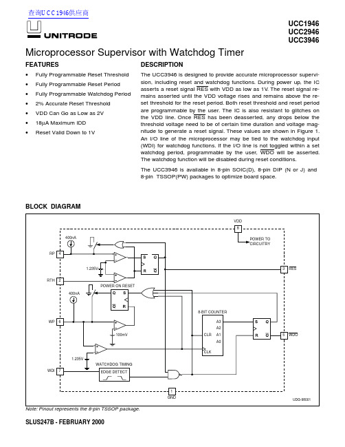
UCC1946UCC2946UCC3946SLUS247B - FEBRUARY 2000FEATURES•Fully Programmable Reset Threshold •Fully Programmable Reset Period •Fully Programmable Watchdog Period •2% Accurate Reset Threshold •VDD Can Go as Low as 2V •18µA Maximum IDD •Reset Valid Down to 1VMicroprocessor Supervisor with Watchdog TimerBLOCK DIAGRAMDESCRIPTIONThe UCC3946is designed to provide accurate microprocessor supervi-sion,including reset and watchdog functions.During power up,the IC asserts a reset signal RES with VDD as low as 1V .The reset signal re-mains asserted until the VDD voltage rises and remains above the re-set threshold for the reset period.Both reset threshold and reset period are programmable by the user.The IC is also resistant to glitches on the VDD line.Once RES has been deasserted,any drops below the threshold voltage need to be of certain time duration and voltage mag-nitude to generate a reset signal.These values are shown in Figure 1.An I/O line of the microprocessor may be tied to the watchdog input (WDI)for watchdog functions.If the I/O line is not toggled within a set watchdog period,programmable by the user,WDO will be asserted.The watchdog function will be disabled during reset conditions.The UCC3946is available in 8-pin SOIC(D),8-pin DIP (N or J)and 8-pin TSSOP(PW) packages to optimize board space.查询UCC1946供应商ELECTRICAL CHARACTERISTICS:Unless otherwise specified,VDD = 2.1V to 5.5V for UCC1946 and UCC2946;VDD = 2V to 5.5V for UCC3946; TA = 0°C to 70°C for UCC3946, –40°C to 95°C for UCC2946, and –55°C to 125°C for UCC1946;T A =T JPARAMETERSTEST CONDITIONSMIN TYP MAXMIN TYPMAX UNITS UCC3946UCC1946 & UCC2946Operating Voltage 2.05.5 2.15.5V Supply Current 10181218µA Minimum VDD (Note 1)1 1.1VReset Section Reset Threshold VDD Rising1.2101.235 1.2601.1701.235 1.260V Threshold Hysteresis 1515mV Input Leakage 55nA Output High Voltage I SOURCE = 2mA V DD –0.3V DD –0.3V Output Low Voltage I SINK = 2mA0.10.1V VDD = 1V,I SINK = 20uA 0.20.4V VDD to Output Delay VDD = -1mV/µs (Note 2)120120µs Reset Period C RP = 64nF160200260140200320msWatchdog Section WDI Input High 0.7·V DD0.7·V DDV WDI Input Low 0.3·V DD 0.3·V DD V Watchdog Period C WP = 64nF1.12 1.602.080.96 1.602.56s Watchdog Pulse Width 5050ns Output High Voltage I SOURCE = 2mA V DD –0.3V DD –0.3V Output Low VoltageI SINK = 2mA 0.10.1VNote 1:This is the minimum supply voltage where RES is considered valid.Note 2:Guaranteed by design.Not 100% tested in production.ABSOLUTE MAXIMUM RATINGSV IN . . . . . . . . . . . . . . . . . . . . . . . . . . . . . . . . . . . . . . . . . . . .10V Storage Temperature . . . . . . . . . . . . . . . . . . .–65°C to +150°C Junction Temperature. . . . . . . . . . . . . . . . . . .–55°C to +150°C Lead Temperature (Soldering, 10 sec.). . . . . . . . . . . . .+300°C Currents are positive into,negative out of the specified terminal.Consult Packaging Section of the Databook for thermal limita-tions and considerations of packages.The UCC3946supervisory circuit provides accurate re-set and watchdog functions for a variety of microproces-sor applications.The reset circuit prevents the microprocessor from executing code during undervoltage conditions,typically during power-up and power-down.In order to prevent erratic operation in the presence of noise,voltage “glitches”whose voltage amplitude and time duration are less than the values specified in Fig.1are ignored.The watchdog circuit monitors the microprocessor’s ac-tivity,if the microprocessor does not toggle WDI during the programmable watchdog period WDO will go low,alerting the microprocessor’s interrupt of a fault.The WDO pin is typically connected to the non-maskable in-put of the microprocessor so that an error recovery rou-tine can be executed.APPLICATION INFORMATIONFigure 1.Overdrive voltage vs.delay to output low on RESB.Slew rate:–1V/mS;monitored voltage =V DD .GND:Ground reference for the IC.RES:This pin is high only if the voltage on the RTH has risen above 1.235V .Once RTH rises above the threshold,this pin remains low for the reset period.This pin will also go low and remain low if the RTH voltage dips below 1.235V for an amount of time determined by Figure 1.RTH:This input compares its voltage to an internal 1.25V reference.By using external resistors,a user can pro-gram any reset threshold he wishes to achieve.RP:This pin allows the user to program the reset period by adjusting an external capacitor.VDD:Supply voltage for the IC.WDI:This pin is the input to the watchdog timer.If this pin is not toggled or strobed within the watchdog period,WDO is asserted.WDO:This pin is the watchdog output.This pin will be asserted low if the WDI pin is not strobed or toggled within the watchdog period.WP:This pin allows the user toprogram the watchdog period by adjusting an external capacitor.PIN DESCRIPTIONSFigure 2.Typical RTH threshold vs.temperature.Figure 3.Typical IDD vs VDD.Programming the Reset Voltage and Reset Period The UCC3946allows the reset trip voltage to be pro-grammed with two external resistors.In most applications VDD is monitored by the reset circuit,however,the de-sign allows voltages other than VDD to be monitored.Referring to Fig.4,the voltage below which reset will be asserted is determined by:V =1.235•R1+R2R2RESET In order to keep quiescent currents low,resistor values in the megaohm range can be used for R1and R2.A man-ual reset can be easily implemented by connecting a mo-mentary push switch in parallel with R2.RES is guaranteed to be low with VDD voltages as low as 1V .Once VDD rises above the programmed threshold,RES remains low for the reset period defined by:T C RP RP=•3125.where T RP is time in milliseconds and C RP is capacitance in nanofarads.C RP is charged with a precision current source of 400nA,a high quality,low leakage capacitor (such as an NPO ceramic)should be used to maintain timing tolerances.Fig.5illustrates the voltage levels and timings associated with the reset circuit.Programming the Watchdog PeriodThe watchdog period is programmed with C WP as fol-lows:T C WP WP=•25where T WP is in milliseconds and C WP is in nanofarads.A high quality,low leakage capacitor should be used for C WP .The watchdog input WDI must be toggled with a high/low or low/high transition within the watchdog period to prevent WDO from assuming a logic level low.WDO will maintain the low logic level until WDI is toggled or RES is asserted.If at any time RES is asserted,WDO will assume a high logic state and the watchdog period will be reinitiated.Fig.6illustrates the timings associated with the watchdog circuit.Figure 4.Typical application diagram.Connecting WDO to RESIn order to provide design flexibility,the reset and watch-dog circuits in the UCC3946have separate outputs.Each output will independently drive high or low,depending on circuit conditions explained previously.In some applications,it may be desirable for either the RES or WDO to reset the microprocessor.This can be done by connecting WDO to RES.If the pins try to drive to different output levels,the low output level will domi-nate.Additional current will flow from VDD to GND during these states.If the application cannot support additional current(during fault conditions),RES and WDO can be connected to the inputs of an OR gate whose output is connected to the microprocessor’s reset yout ConsiderationsA0.1µF capacitor connected from V DD to GND is recom-mended to decouple the UCC3946from switching tran-sients on the V DD supply rail.Since RP and WP are precision current sources,capaci-tors C RP and C WP should be connected to these pins with minimal trace length to reduce board capacitance. Care should be taken to route any traces with high volt-age potential or high speed digital signals away from these capacitors.Resistors R1and R2generally have a high ohmic value, traces associated with these parts should be kept short in order to prevent any transient producing signals from coupling into the high impedance RTH pin.Figure 5.Reset circuit timings.Figure 6.Watchdog circuit timings. UNITRODE CORPORA TION7 CONTINENT AL BLVD.• MERRIMACK, NH 03054TEL.(603) 424-2410 • FAX (603) 424-3460。
AEMC PowerPad Model 3945 三相电力质量分析仪说明书
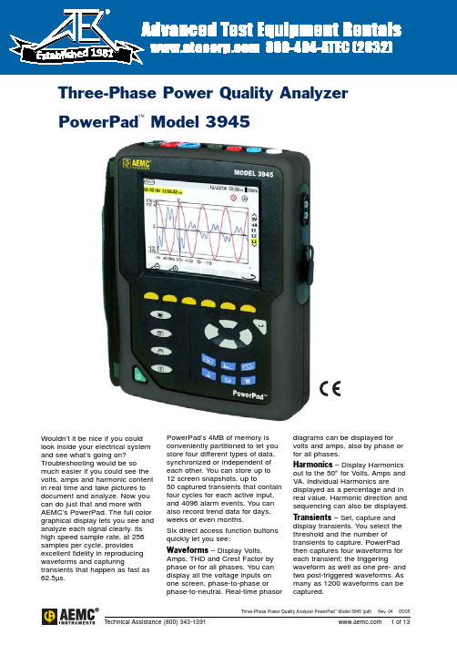
Three-Phase Power Quality Analyzer PowerPa d™Model 39451981Three-Phase Power Quality Analyzer PowerPad Model 3945 (pdf)Rev. 0405/05Technical Assistance (800) 2of 13Alarms –Configure, capture and display up to 4096 alarm events based on up to ten different trigger variables. Each captured alarm event will show the phase, the variable and the value as well as the time and duration.Record – Set up and record trend data at selectable rates from one sample/second to one sample every 15 minutes on as many as 22 different variables for allphases. See the recorded data on screen, zoom in and out and scroll the time axis to analyze the data.Power & Energy – Display Watts, VARs and VA by phase and total. Accumulate totals and see whether the energy is inductive or capacitive.If you’re not convinced yet,consider these other functions and features:•PowerPad uses current probes that auto configure theinstrument’s current channel for range and scale.•PowerPad comes with an online help system that gives you clear information about the functions and buttons for each screen.•PowerPad comes with all options and accessories needed to capture, display, download,analyze and store data. No add-on accessories are required that increase your cost. PowerPad is supplied with AEMC’s DataView ®Professional graphing/analysis software package at noadditional cost (a $395.00 value).The software lets you completely configure and capture data in real time on your computer. You can download all stored data from PowerPad and print reports from a library of pre-designed templates or create your own custom templates and reports.In addition to all of this, PowerPad speaks six different languages. At the press of a button, information can be displayed in English,Spanish, French, Portuguese,Italian and German.Arrange for a demonstration today!Tilt-out bail facilitates bench top operation for convenient viewing of display.Three-Phase Power Quality Analyzer PowerPad Model 3945 (pdf)Rev. 0405/05Technical Assistance (800) 3of 13Features•True RMS single-, two- and three-phasemeasurements at 256 samples/cycle, plus DC •Real-time color waveforms •Easy-to-use on-screen setup•Automatic current probe recognition and scaling •True RMS voltage and current measurement •Measures DC volts, amps and power•Display and capture voltage, current and powerharmonics to 50th order, including direction, in real time •Capture transients down to 1/256th of a cycle •Phasor diagram display •Peak voltage and current•Nominal frequency from 40 to 70Hz •VA, VAR and W per phase and total •kVAh, VARh and kWh per phase and total •Neutral current display for three-phase •Crest factors for current and voltage •Transformer K-factor display•Power Factor, displacement PF display •Captures up to 50 transients •Short-term flicker display•Phase unbalance (current and voltage)•Harmonic Distortion (total and individual) from 1st to 50th •Alarms, surges and sags•Records date and characteristics of disturbances •Immediate printout directly to a printer•Screen snapshot function captures waveforms or other information on the display •Optically isolated RS-23 communication port •Includes DataView ®Professional software for data storage, analysis and report generation •EN 61010, 600V Cat. IIIApplications•Verification of power distribution circuits•Measurement and recording of power system quality (kW, VA, VAR)•Energy metering (kVAh,VARh, kWh)•In plant troubleshooting of power distribution panels and individual machinery •Monitor pad mount transformers•Determine harmonic problems originating from source or load •Monitor phase unbalances •Determine transformer K-factor •And much, much morePower quality analysis on a three-phase panel using the AmpFlex ™flexible current probes.Measure all three phases of voltage and current simultaneously.Three-Phase Power Quality Analyzer PowerPad Model 3945 (pdf)Rev. 0405/05Technical Assistance (800) 4of 13transients can be stored, each consisting of four cycles and up to six inputs for aand displayed by selecting it from the list.PowerPad’s direct access system lets you see the important information you need at the press of a button.Quickly review waveforms,harmonics,transients,alarms and recorded data on screen.Setup is straightforward using a combination of graphic and text prompts to quickly configure PowerPad for the job site.Three-Phase Power Quality Analyzer PowerPad Model 3945 (pdf)Rev. 0405/05Technical Assistance (800) 5of 13Power & Energy ModeSpecificationsThree-Phase Power Quality Analyzer PowerPad Model 3945 (pdf)Rev. 0405/05 Technical Assistance (800) 6of 13Three-Phase Power Quality Analyzer PowerPad Model 3945 (pdf)Rev. 0405/05Technical Assistance (800) 7of 13FeaturesConfigure all functions of the PowerPad ™Model 3945•Display and analyze real-time data on your PC •Configure all PowerPad functions and parameters from your PC •Customize views, templates and reports to your exact needs •Create and store a complete library of configurations that can be up-loaded to the PowerPad as needed •Zoom in and out and pan through sections of the graph to analyze the data •Display waveforms, trend graphs,harmonic spectrums, text summaries, transients, event logs and stored alarms •Print reports using standard or custom templates you designMinimum System Requirements•Windows ®98/2000/ME/XP or Windows ®NT 4.0•128MB of RAM(256MB recommended) for Windows ®98/2000/ME or Windows ®NT 4.0256MB of RAM for Windows ®XP •35MB of hard disk space (200MB recommended)•CD Rom DriveDataView ®Professional SoftwareDisplay waveforms in real time on your computer.The DataView Professional Software provides a convenient way to configure and control power analysis tests from your computer. Through the use of clear and easy-to-use tabbed dialog boxes, allPowerPad functions can be configured andtests can be initiated. Results can be displayed in real time and stored in yourPC. Reports may be printed along withthe operator’s comments andanalysis.DataView Professional is included with the PowerPad Model 3945.Three-Phase Power Quality Analyzer PowerPad Model 3945 (pdf)Rev. 0405/05Technical Assistance (800) 8of 13Display all harmonics from 1st to 50th in bargraph form for voltage,current and power.Display power and energy parameters – both instantaneous and total.Display harmonics in a text table from harmonic 0 (DC) through the 50th .Clear and easy setup of all functions from one tabbed dialog box.Display real-time waveforms by phase, parameter or total.Display real-time phasor diagrams.Includes unbalance for both voltage and current.Reports can be displayed on yourPC and printed.Each report includesall test results in a tabular and graphicformat,as well as operator and testsite ments typed bythe operator will also be included.Three-Phase Power Quality Analyzer PowerPad Model 3945 (pdf)Rev. 0405/05 Technical Assistance (800) 9of 13Three-Phase Power Quality Analyzer PowerPad Model 3945 (pdf)Rev. 0405/05Technical Assistance (800) 10of 13ConstructionThe color-coded input connectors provide dedicated current probe inputs and voltage inputs.The connections located on the side of the Model 3945 provide optically isolated RS-232communication port and line power from 85 to 256V AC (50/60Hz).1/4VGA (320 x 240)Color LCDLine power connectorHand strapCurrent probeinputsCurrent probeinputsSix variable function buttonsInstrument configurationbutton Snapshot buttonPrint button Help button ON/OFF buttonLine power connectorVoltage inputsVoltage inputsOptically coupled bi-directional RS-232 portOptically coupled bi-directional RS-232 portEnter buttonDirect display mode buttonsDirt resistant overmoldCursor movement,browsing andselection buttonsThree-Phase Power Quality Analyzer PowerPad Model 3945 (pdf)Rev. 0405/05Technical Assistance (800) 11of 13AccessoriesMax conductor size:2.05" (52mm)Measurement range:3 to 1200AMax conductor size:0.78" (20mm)Measurement ranges:5mA to 6A100mA to 120AMax conductor size:11.46" (290mm)Measurement range:9 to 6500AMax conductor size:7.64" (190mm)Measurement range:9 to 6500AMax conductor size:0.78" (20mm)Measurement range:0.5 to 240AMax conductor size:1.6" (41mm)Measurement ranges:10 to 1000A AC10 to 1400A DCThe 5A Adapter Box facilitates theuse of current probes with current outputs for use withPowerPad.Ratios areprogrammable up to 2999:1 or 2999:5.The Adapter Box works with single-,two- or three-phasecurrent inputs.MN93SR193193-24193-36MN193MR193Max conductor size:1.6" (41mm)Measurement ranges:10 to 1000A 10 to 1400A MR193Ordering InformationAll models include three color-coded current probes (MN93 example shown),four color-coded 10 ft voltage leads, four color-coded alligator clips,RS-232 DB9F optically coupled serial cable, NiMH battery, US 120V power cord,DataView Professional software, carrying bag, soft carrying pouch and user manual.Contact UsUnited States & Canada:Chauvin Arnoux®, Inc.d.b.a. AEMC®Instruments200 Foxborough Blvd.Foxborough, MA02035 USA(508) 698-2115 • Fax (508) 698-2118Customer Support – for placing an order, obtaining price & delivery:************************Sales Department – for general sales information:**************Repair and Calibration Service – for information on repair & calibration, obtaining a user manual:***************Technical and Product Application Support – for technical and application support:*****************Webmaster – for information regarding :******************South America, Central America, Mexico, Caribbean, Australia &New Zealand:Chauvin Arnoux®, Inc.d.b.a. AEMC®Instruments15 Faraday DriveDover, NH 03820 USA(978) 526-7667 • Fax (978) 526-7605***************All other countries:Chauvin Arnoux SCA190, rue Championnet75876 Paris Cedex 18, France33 1 44 85 45 28 • Fax 33 1 46 27 73 89***********************Three-Phase Power Quality Analyzer PowerPad Model 3945 (pdf)Rev. 0405/05 Technical Assistance (800) 13of 13。
A3946KLB-T资料
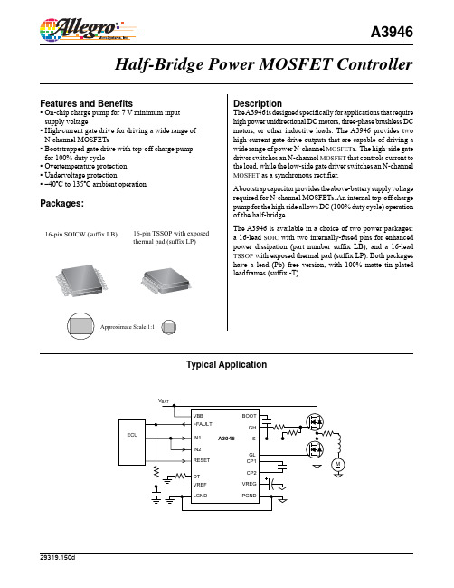
–
Rdead = 5 kΩ Rdead = 100 kΩ Logic input to unloaded GH, GL. DT = VREF
trise tfall RDSUP
RDSDOWN VGH VGL
tDEAD tPD
RESET = High, Outputs Low RESET = Low VBB > 7.75 V, Ireg = 0 mA to 15 mA VBB = 7 V to 7.75 V, Ireg = 0 mA to 15 mA CP1, CP2 IREF ≤ 4 mA, CREF = 0.1 μF VBOOT – VS = 8.5 V
▪ Bootstrapped gate drive with top-off charge pump for 100% duty cycle
▪ Overtemperature protection ▪ Undervoltage protection ▪ –40ºC to 135ºC ambient operation
Pullup On Resistance
Pulldown On Resistance
GH Output Voltage GL Output Voltage Timing Dead Time (Delay from Turn Off to Turn On) Propagation Delay
IVBB
舒瑞普(传特)技术文档
舒瑞普/传特板式换热器国际公司是全球知名的拼装式(PHE)及钎焊式(CB E)板式换热器专业生产商,为石油化工、机械工业、汽车工业、食品工业、电力、冶金、造船业、暖通、空调制冷行业提供产品和服务。
舒瑞普/传特的产品高度从286mm—4392mm,宽度从114mm—1540mm,接口直径从DN25—DN500,板片厚度从0.4mm—1.0mm,众多系列,数十种型号;最大流量可达4250m³/h;最大换热面积可达1840㎡;最高功罪压力可达2.5MPa;最工作温度可达180℃。
舒瑞普公司目前生产近70种不同规格的板式换热器,为您提供GC、GD、GF、GX、GL、GW系列产品,是迄今为止品种规格最全的板式换热器制造商。
舒瑞普/传特板式换热器有不锈钢SUS304,SUS316L、Ti、Hadtelloy Alloy、Nickel等多种板片材质,适用于各种工况。
在垫片方面提供了NBR、HNBR、EPDM、Viton、NEOPRENE、Silicon Ru bbe等材质。
适用于不同工况需求,确保您得到最适合您工况应用的那一台换热器。
四.板式换热器产品系列﹡同一板片上2种不同的波纹角度﹡垫片槽底部在板片波纹高度的中心平面上﹡两种板片可以组合成6种流道排列﹡高效率的对角流布置﹡接口从DN50-DN500。
﹡综合了GX型板片密封垫片槽的巧妙设计,板片波纹相对中线对称分布,垫片槽深度为波纹深度的一半,垫片槽底部位于波纹板片的中心平面上,科学的设计保证了密封的可靠性。
﹡高性能的对角流设计。
﹡可应用于各个行业。
﹡板片的波纹节距是普通板片波纹节距地2-5倍,允许不规则的固体颗粒自由通过而避免堵塞,波纹节距范围为8~16mm。
﹡宽流道板式换热器专门适用于含有纤维或粘附性颗粒的易堵塞介质。
﹡应用于造纸、食品粗加工、化纤、纺织、制糖、乳胶等等行业。
板式换热器设计选型须知:(1)板式换热器固有特性,如板片材料、密封胶垫等。
- 1、下载文档前请自行甄别文档内容的完整性,平台不提供额外的编辑、内容补充、找答案等附加服务。
- 2、"仅部分预览"的文档,不可在线预览部分如存在完整性等问题,可反馈申请退款(可完整预览的文档不适用该条件!)。
- 3、如文档侵犯您的权益,请联系客服反馈,我们会尽快为您处理(人工客服工作时间:9:00-18:30)。
NST3946DP6T5GDual Complementary General Purpose Transistor The NST3946DP6T5G device is a spin−off of our popular SOT−23/SOT−323/SOT−563 three−leaded device. It is designed for general purpose amplifier applications and is housed in the SOT−963 six−leaded surface mount package. By putting two discrete devices in one package, this device is ideal for low−power surface mount applications where board space is at a premium.Features•h FE, 100−300•Low V CE(sat), ≤ 0.4 V•Simplifies Circuit Design•Reduces Board Space•Reduces Component Count•This is a Pb−Free DeviceMAXIMUM RATINGSRating Symbol Value Unit Collector−Emitter Voltage V CEO40Vdc Collector−Base Voltage V CBO60Vdc Emitter−Base Voltage V EBO 6.0Vdc Collector Current − Continuous I C200mAdcElectrostatic Discharge HBMMM ESDClass2BTHERMAL CHARACTERISTICSCharacteristic (Single Heated)Symbol Max UnitTotal Device Dissipation T A = 25°C Derate above 25°C (Note 1)P D2401.9mWmW/°CThermal Resistance, Junction-to-Ambient (Note 1)R q JA520°C/WTotal Device Dissipation T A = 25°C Derate above 25°C (Note 2)PD2802.2mWmW/°CThermal Resistance, Junction-to-Ambient(Note 2)R q JA446°C/W Characteristic (Dual Heated) (Note 3)Symbol Max UnitTotal Device Dissipation T A = 25°C Derate above 25°C (Note 1)P D3502.8mWmW/°CThermal Resistance, Junction-to-Ambient(Note 1)R q JA357°C/WTotal Device Dissipation T A = 25°C Derate above 25°C (Note 2)P D4203.4mWmW/°CThermal Resistance, Junction-to-Ambient(Note 2)R q JA297°C/WJunction and Storage Temperature Range T J, T stg−55 to+150°CStresses exceeding Maximum Ratings may damage the device. Maximum Ratings are stress ratings only. Functional operation above the Recommended Operating Conditions is not implied. Extended exposure to stresses above the Recommended Operating Conditions may affect device reliability.1.FR−4 @ 100 mm2, 1 oz. copper traces, still air.2.FR−4 @ 500 mm2, 1 oz. copper traces, still air.3.Dual heated values assume total power is sum of two equally powered channelsQ2NST3946DP6T5G*ORDERING INFORMATION*Q1 PNPQ2 NPNDevice Package Shipping†NST3946DP6T5G SOT−963(Pb−Free)8000/Tape & ReelSOT−963CASE 527ADPLASTICMARKING DIAGRAML= Device Code(180° Clockwise Rotation)M= Date CodeG= Pb−Free PackageM GG1(Note: Microdot may be in either location)†For information on tape and reel specifications, including part orientation and tape sizes, please refer to our T ape and Reel Packaging Specifications Brochure, BRD8011/D.3LELECTRICAL CHARACTERISTICS (T A = 25°C unless otherwise noted)Characteristic Symbol Min Max Unit OFF CHARACTERISTICSCollector−Emitter Breakdown Voltage (Note 4)(I C = 1.0 mAdc, I B = 0)(NPN) (I C = −1.0 mAdc, I B = 0)(PNP)V(BR)CEO40−40−−VdcCollector−Base Breakdown Voltage(I C = 10 m Adc, I E = 0)(NPN) (I C = −10 m Adc, I E = 0)(PNP)V(BR)CBO60−40−−VdcEmitter−Base Breakdown Voltage(I E = 10 m Adc, I C = 0)(NPN) (I E = −10 m Adc, I C = 0)(PNP)V(BR)EBO6.0−5.0−−VdcCollector Cutoff Current(V CE = 30 Vdc, V EB = 3.0 Vdc)(NPN) (V CE = −30 Vdc, V EB = −3.0 Vdc)(PNP)I CEX−−50−50nAdcON CHARACTERISTICS (Note 4)DC Current Gain(I C = 0.1 mAdc, V CE = 1.0 Vdc)(NPN) (I C = 1.0 mAdc, V CE = 1.0 Vdc)(I C = 10 mAdc, V CE = 1.0 Vdc)(I C = 50 mAdc, V CE = 1.0 Vdc)(I C = 100 mAdc, V CE = 1.0 Vdc)(I C = −0.1 mAdc, V CE = −1.0 Vdc)(PNP) (I C = −1.0 mAdc, V CE = −1.0 Vdc)(I C = −10 mAdc, V CE = −1.0 Vdc)(I C = −50 mAdc, V CE = −1.0 Vdc)(I C = −100 mAdc, V CE = −1.0 Vdc)h FE4070100603060801006030−−300−−−−300−−−Collector−Emitter Saturation Voltage(I C = 10 mAdc, I B = 1.0 mAdc)(NPN) (I C = 50 mAdc, I B = 5.0 mAdc)(I C = −10 mAdc, I B = −1.0 mAdc)(PNP) (I C = −50 mAdc, I B = −5.0 mAdc)V CE(sat)−−−−0.20.3−0.25−0.4VdcBase−Emitter Saturation Voltage(I C = 10 mAdc, I B = 1.0 mAdc)(NPN) (I C = 50 mAdc, I B = 5.0 mAdc)(I C = −10 mAdc, I B = −1.0 mAdc)(PNP) (I C = −50 mAdc, I B = −5.0 mAdc)V BE(sat)0.65−−0.65−0.850.95−0.85−0.95Vdc4.Pulse Test: Pulse Width ≤300 μs; Duty Cycle ≤2.0%.ELECTRICAL CHARACTERISTICS (T A = 25°C unless otherwise noted) (Continued)CharacteristicSymbolMinMaxUnitSMALL −SIGNAL CHARACTERISTICSCurrent −Gain − Bandwidth Product(I C = 10 mAdc, V CE = 20 Vdc, f = 100 MHz)(NPN)(I C = −10 mAdc, V CE = −20 Vdc, f = 100 MHz)(PNP)f T200250−−MHzOutput Capacitance(V CB = 5.0 Vdc, I E = 0, f = 1.0 MHz)(NPN)(V CB = −5.0 Vdc, I E = 0, f = 1.0 MHz)(PNP)C obo−− 4.04.5pFInput Capacitance(V EB = 0.5 Vdc, I C = 0, f = 1.0 MHz)(NPN)(V EB = −0.5 Vdc, I C = 0, f = 1.0 MHz)(PNP)C ibo−−8.010.0pFNoise Figure(V CE = 5.0 Vdc, I C = 100 m Adc, R S = 1.0 k Ω, f = 1.0 kHz)(NPN)(V CE = −5.0 Vdc, I C = −100 m Adc, R S = 1.0 k Ω, f = 1.0 kHz)(PNP)NF−−5.04.0dBSWITCHING CHARACTERISTICSDelay Time (V CC = 3.0 Vdc, V BE = −0.5 Vdc)(NPN)(V CC = −3.0 Vdc, V BE = 0.5 Vdc)(PNP)t d −−3535nsRise Time (I C = 10 mAdc, I B1 = 1.0 mAdc)(NPN)(I C = −10 mAdc, I B1 = −1.0 mAdc)(PNP)t r −−3535Storage Time (V CC = 3.0 Vdc, I C = 10 mAdc)(NPN)(V CC = −3.0 Vdc, I C = −10 mAdc)(PNP)t s −−275250nsFall Time(I B1 = I B2 = 1.0 mAdc)(NPN)(I B1 = I B2 = −1.0 mAdc)(PNP)t f−−5050NPN TRANSISTORI C , COLLECTOR CURRENT (A)Figure 1. Collector Emitter Saturation Voltage vs.Collector CurrentFigure 2. DC Current Gain vs. Collector CurrentI C , COLLECTOR CURRENT (A)V C E (s a t ), C O L L E C T O R −E M I T T E R S A T U R A T I O N V O L T A G E (V )h F E , D C C U R R E N T G A I N (V )Figure 3. Base Emitter Saturation Voltage vs.Collector CurrentFigure 4. Base Emitter Turn −On Voltage vs.Collector CurrentI C , COLLECTOR CURRENT (A)I C , COLLECTOR CURRENT (A)0.30.40.50.60.70.91.01.1Figure 5. Saturation RegionFigure 6. Input CapacitanceI b , BASE CURRENT (A)V eb , EMITTER BASE VOLTAGE (V)3.54.04.55.56.07.07.58.0Figure 7. Output CapacitanceV cb , COLLECTOR BASE VOLTAGE (V)V B E (s a t ), B A S E −E M I T T E R S A T U R A T I O N V O L T A G E (V )V B E (o n ), B A S E −E M I T T E R T U R N −O N V O L T A G E (V )V C E (s a t ), C O L L E C T O R −E M I T T E R S A T U R A T I O N V O L T A G E (V )C i b o , I N P U T C A P A C I T A N C E (p F )C o b o , O U T P U T C A P A C I T A N C E (p F )0.85.06.5I C , COLLECTOR CURRENT (A)Figure 8. Collector Emitter Saturation Voltage vs.Collector CurrentFigure 9. DC Current Gain vs. Collector CurrentI C , COLLECTOR CURRENT (A)V C E (s a t ), C O L L E C T O R −E M I T T E R S A T U R A T I O N V O L T A G E (V )h F E , D C C U R R E N T G A I N (V )Figure 10. Base Emitter Saturation Voltage vs.Collector CurrentFigure 11. Base Emitter Turn −On Voltage vs.Collector CurrentI C , COLLECTOR CURRENT (A)I C , COLLECTOR CURRENT (A)0.30.40.50.60.70.91.01.1Figure 12. Saturation RegionFigure 13. Input CapacitanceI b , BASE CURRENT (A)V eb , EMITTER BASE VOLTAGE (V)3.04.06.07.09.0Figure 14. Output CapacitanceV cb , COLLECTOR BASE VOLTAGE (V)V B E (s a t ), B A S E −E M I T T E R S A T U R A T I O N V O L T A G E (V )V B E (o n ), B A S E −E M I T T E R T U R N −O N V O L T A G E (V )V C E (s a t ), C O L L E C T O R −E M I T T E R S A T U R A T I O N V O L T A G E (V )C i b o , I N P U T C A P A C I T A N C E (p F )C o b o , O U T P U T C A P A C I T A N C E (p F )0.85.08.0PACKAGE DIMENSIONSSOT −963CASE 527AD −01ISSUE C*For additional information on our Pb −Free strategy and solderingdetails, please download the ON Semiconductor Soldering and Mounting Techniques Reference Manual, SOLDERRM/D.SOLDERING FOOTPRINT*DIM MIN NOM MAX MILLIMETERS A 0.340.370.40b 0.100.150.20C 0.070.120.17D 0.95 1.00 1.05E 0.750.800.85e 0.35 BSC L 0.050.100.150.95 1.00 1.05H E0.0040.0060.0080.0030.0050.0070.0370.0390.0410.030.0320.0340.014 BSC0.0020.0040.0060.0370.0390.041MIN NOM MAXINCHES NOTES:1.DIMENSIONING AND TOLERANCING PER ANSI Y14.5M, 1982.2.CONTROLLING DIMENSION: MILLIMETERS3.MAXIMUM LEAD THICKNESS INCLUDES LEAD FINISH THICKNESS. MINIMUM LEAD THICKNESS IS THE MINIMUM THICKNESS OF BASE MATERIAL.ǒmm inchesǓSCALE 20:1ON Semiconductor and are registered trademarks of Semiconductor Components Industries, LLC (SCILLC). SCILLC reserves the right to make changes without further notice to any products herein. SCILLC makes no warranty, representation or guarantee regarding the suitability of its products for any particular purpose, nor does SCILLC assume any liability arising out of the application or use of any product or circuit, and specifically disclaims any and all liability, including without limitation special, consequential or incidental damages.“Typical” parameters which may be provided in SCILLC data sheets and/or specifications can and do vary in different applications and actual performance may vary over time. All operating parameters, including “Typicals” must be validated for each customer application by customer’s technical experts. SCILLC does not convey any license under its patent rights nor the rights of others. SCILLC products are not designed, intended, or authorized for use as components in systems intended for surgical implant into the body, or other applications intended to support or sustain life, or for any other application in which the failure of the SCILLC product could create a situation where personal injury or death may occur. Should Buyer purchase or use SCILLC products for any such unintended or unauthorized application, Buyer shall indemnify and hold SCILLC and its officers, employees, subsidiaries, affiliates,and distributors harmless against all claims, costs, damages, and expenses, and reasonable attorney fees arising out of, directly or indirectly, any claim of personal injury or death associated with such unintended or unauthorized use, even if such claim alleges that SCILLC was negligent regarding the design or manufacture of the part. SCILLC is an Equal Opportunity/Affirmative Action Employer. This literature is subject to all applicable copyright laws and is not for resale in any manner.PUBLICATION ORDERING INFORMATION分销商库存信息: ONSEMINST3946DP6T5G。
