ITR9908中文资料
AT90PWM2_08资料

Features•High Performance, Low Power AVR ® 8-bit Microcontroller •Advanced RISC Architecture–129 Powerful Instructions - Most Single Clock Cycle Execution –32 x 8 General Purpose Working Registers–Fully Static Operation–Up to 1 MIPS throughput per MHz–On-chip 2-cycle Multiplier•Data and Non-Volatile Program Memory–8K Bytes Flash of In-System Programmable Program Memory•Endurance: 10,000 Write/Erase Cycles–Optional Boot Code Section with Independent Lock Bits•In-System Programming by On-chip Boot Program•True Read-While-Write Operation–512 Bytes of In-System Programmable EEPROM•Endurance: 100,000 Write/Erase Cycles–512 Bytes Internal SRAM–Programming Lock for Flash Program and EEPROM Data Security•On Chip Debug Interface (debugWIRE)•Peripheral Features–Two or three 12-bit High Speed PSC (Power Stage Controllers) with 4-bitResolution Enhancement•Non Overlapping Inverted PWM Output Pins With Flexible Dead-Time•Variable PWM duty Cycle and Frequency•Synchronous Update of all PWM Registers•Auto Stop Function for Event Driven PFC Implementation•Less than 25 Hz Step Width at 150 kHz Output Frequency•PSC2 with four Output Pins and Output Matrix–One 8-bit General purpose Timer/Counter with Separate Prescaler and Capture Mode–One 16-bit General purpose Timer/Counter with Separate Prescaler, Compare Mode and Capture Mode–Programmable Serial USART•Standard UART mode•16/17 bit Biphase Mode for DALI Communications–Master/Slave SPI Serial Interface–10-bit ADC•Up To 11 Single Ended Channels and 2 Fully Differential ADC Channel Pairs •Programmable Gain (5x, 10x, 20x, 40x on Differential Channels)•Internal Reference Voltage–10-bit DAC–Two or three Analog Comparator with Resistor-Array to Adjust ComparisonVoltage–4 External Interrupts–Programmable Watchdog Timer with Separate On-Chip Oscillator•Special Microcontroller Features–Low Power Idle, Noise Reduction, and Power Down Modes–Power On Reset and Programmable Brown Out Detection–Flag Array in Bit-programmable I/O Space (4 bytes)Microcontroller with 8K Bytes In-System Programmable AT90PWM2AT90PWM3AT90PWM2B AT90PWM3B Summary24317IS–AVR–01/08AT90PWM2/3/2B/3B–In-System Programmable via SPI Port –Internal Calibrated RC Oscillator ( 8 MHz)–On-chip PLL for fast PWM ( 32 MHz, 64 MHz) and CPU (16 MHz)•Operating Voltage: 2.7V - 5.5V •Extended Operating Temperature:–-40°C to +105°1.HistoryThis datasheet deals with product characteristics of AT90PW2 and AT90WM3. It will be updated as soon as characterization will be done.2.DisclaimerTypical values contained in this datasheet are based on simulations and characterization of other AVR microcontrollers manufactured on the same process technology. Min and Max val-ues will be available after the device is characterized.Product Package 12 bit PWM with deadtime ADC Input ADC Diff Analog Compar ApplicationAT90PWM2AT90PWM2B SO24 2 x 2812One fluorescent ballast AT90PWM3AT90PWM3BSO32, QFN323 x 21123HID ballast, fluorescent ballast, Motor controlProduct RevisionAT90PWM2AT90PWM3First revision of parts, only for running production.AT90PWM2B AT90PWM3BSecond revision of parts, for all new developments.The major changes are :•complement the PSCOUT01, PSCOUT11, PSCOUT21 polarity in centered mode - See “PSCn0 & PSCn1 Basic Waveforms in Center Aligned Mode” on page 139.•Add the PSC software triggering capture - See “PSC 0 Input Capture Register – PICR0H and PICR0L” on page 170.•Add bits to read the PSC output activity - See “PSC0 Interrupt Flag Register – PIFR0” on page 172.•Add some clock configurations - See “Device Clocking Options Select AT90PWM2B/3B” on page 31.•Change Amplifier Synchonization - See “Amplifier” on page 252. and See “” on page 254.•Correction of the Errata - See “Errata” on page 23.34317IS–AVR–01/08AT90PWM2/3/2B/3B3.Pin Configurations44317IS–AVR–01/08AT90PWM2/3/2B/3BFigure 3-3.QFN32 (7*7 mm) Package.3.1Pin Descriptions:Table 3-1.Pin out descriptionS024 Pin NumberSO32 Pin NumberQFN32 Pin NumberMnemonic Type Name, Function & Alternate Function795GND Power Ground: 0V reference182420AGNDPowerAnalog Ground: 0V reference for analog part54317IS–AVR–01/08AT90PWM2/3/2B/3B684VCCpowerPower Supply:172319AVCC PowerAnalog Power Supply: This is the power supply voltage for analog partFor a normal use this pin must be connected.192521AREF PowerAnalog Reference : reference for analog converter . This is the reference voltage of the A/D converter. As output, can be used by external analog8128PBO I/OMISO (SPI Master In Slave Out)PSCOUT20 output9139PB1I/OMOSI (SPI Master Out Slave In)PSCOUT21 output162016PB2I/O ADC5 (Analog Input Channel5 )INT1202723PB3I/O AMP0- (Analog Differential Amplifier 0 Input Channel )212824PB4I/O AMP0+ (Analog Differential Amplifier 0 Input Channel )223026PB5I/OADC6 (Analog Input Channel 6)INT 2233127PB6I/O ADC7 (Analog Input Channel 7)ICP1B (Timer 1 input capture alternate input)PSCOUT11 output (see note 1)243228PB7I/O PSCOUT01 outputADC4 (Analog Input Channel 4)SCK (SPI Clock)NA230PC0I/OPSCOUT10 output (see note 1) INT373PC1I/OPSCIN1 (PSC 1 Digital Input) OC1B (Timer 1 Output Compare B)106PC2I/OT0 (Timer 0 clock input)PSCOUT22 output 117PC3I/O T1 (Timer 1 clock input)PSCOUT23 output2117PC4I/OADC8 (Analog Input Channel 8)AMP1- (Analog Differential Amplifier 1 Input Channel )2218PC5I/OADC9 (Analog Input Channel 9)AMP1+ (Analog Differential Amplifier 1 Input Channel )2622PC6I/O ADC10 (Analog Input Channel 10)ACMP1 (Analog Comparator 1 Positive Input )2925PC7I/OD2A : DAC outputTable 3-1.Pin out description (Continued)S024 Pin NumberSO32 Pin NumberQFN32 Pin NumberMnemonic Type Name, Function & Alternate Function64317IS–AVR–01/08AT90PWM2/3/2B/3B1.PSCOUT10 & PSCOUT11 are not present on 24 pins package4.OverviewThe AT90PWM2/2B/3/3B is a low-power CMOS 8-bit microcontroller based on the AVR enhanced RISC architecture. By executing powerful instructions in a single clock cycle, the AT90PWM2/2B/3/3B achieves throughputs approaching 1 MIPS per MHz allowing the system designer to optimize power consumption versus processing speed.1129PD0I/O PSCOUT00 outputXCK (UART Transfer Clock)SS_A (Alternate SPI Slave Select)3432PD1I/OPSCIN0 (PSC 0 Digital Input )CLKO (System Clock Output)451PD2I/O PSCIN2 (PSC 2 Digital Input)OC1A (Timer 1 Output Compare A)MISO_A (Programming & alternate SPI Master In Slave Out)562PD3I/OTXD (Dali/UART Tx data)OC0A (Timer 0 Output Compare A)SS (SPI Slave Select)MOSI_A (Programming & alternate Master Out SPI Slave In)121612PD4I/OADC1 (Analog Input Channel 1)RXD (Dali/UART Rx data)ICP1A (Timer 1 input capture)SCK_A (Programming & alternate SPI Clock)131713PD5I/OADC2 (Analog Input Channel 2)ACMP2 (Analog Comparator 2 Positive Input )141814PD6I/O ADC3 (Analog Input Channel 3 )ACMPM reference for analog comparators INT0151915PD7I/O ACMP0 (Analog Comparator 0 Positive Input )2331PE0I/O or IRESET (Reset Input)OCD (On Chip Debug I/O)101410PE1I/OXTAL1: XTAL InputOC0B (Timer 0 Output Compare B)111511PE2I/OXTAL2: XTAL OuTputADC0 (Analog Input Channel 0)Table 3-1.Pin out description (Continued)S024 Pin NumberSO32 Pin NumberQFN32 Pin NumberMnemonicTypeName, Function & Alternate Function74317IS–AVR–01/08AT90PWM2/3/2B/3B4.1Block DiagramFigure 4-1.Block DiagramThe AVR core combines a rich instruction set with 32 general purpose working registers. All the 32 registers are directly connected to the Arithmetic Logic Unit (ALU), allowing two independent registers to be accessed in one single instruction executed in one clock cycle. The resulting architecture is more code efficient while achieving throughputs up to ten times faster than con-ventional CISC microcontrollers.The AT90PWM2/2B/3/3B provides the following features: 8K bytes of In-System Programmable Flash with Read-While-Write capabilities, 512 bytes EEPROM, 512 bytes SRAM, 53 general purpose I/O lines, 32 general purpose working registers,three Power Stage Controllers, two flex-ible Timer/Counters with compare modes and PWM, one USART with DALI mode, an 11-channel 10-bit ADC with two differential input stage with programmable gain, a 10-bit DAC, a programmable Watchdog Timer with Internal Oscillator, an SPI serial port, an On-chip Debug system and four software selectable power saving modes.84317IS–AVR–01/08AT90PWM2/3/2B/3BThe Idle mode stops the CPU while allowing the SRAM, Timer/Counters, SPI ports and interrupt system to continue functioning. The Power-down mode saves the register contents but freezes the Oscillator, disabling all other chip functions until the next interrupt or Hardware Reset. The ADC Noise Reduction mode stops the CPU and all I/O modules except ADC, to minimize switch-ing noise during ADC conversions. In Standby mode, the Crystal/Resonator Oscillator is running while the rest of the device is sleeping. This allows very fast start-up combined with low power consumption.The device is manufactured using Atmel’s high-density nonvolatile memory technology. The On-chip ISP Flash allows the program memory to be reprogrammed in-system through an SPI serial interface, by a conventional nonvolatile memory programmer, or by an On-chip Boot program running on the AVR core. The boot program can use any interface to download the application program in the application Flash memory. Software in the Boot Flash section will continue to run while the Application Flash section is updated, providing true Read-While-Write operation. By combining an 8-bit RISC CPU with In-System Self-Programmable Flash on a monolithic chip,the Atmel AT90PWM2/3 is a powerful microcontroller that provides a highly flexible and cost effective solution to many embedded control applications.The AT90PWM2/3 AVR is supported with a full suite of program and system development tools including: C compilers, macro assemblers, program debugger/simulators, in-circuit emulators,and evaluation kits.4.2Pin Descriptions4.2.1VCCDigital supply voltage.4.2.2GNDGround.4.2.3Port B (PB7..PB0)Port B is an 8-bit bi-directional I/O port with internal pull-up resistors (selected for each bit). The Port B output buffers have symmetrical drive characteristics with both high sink and source capability. As inputs, Port B pins that are externally pulled low will source current if the pull-up resistors are activated. The Port B pins are tri-stated when a reset condition becomes active,even if the clock is not running.Port B also serves the functions of various special features of the AT90PWM2/2B/3/3B as listed on page 69.4.2.4Port C (PC7..PC0)Port C is an 8-bit bi-directional I/O port with internal pull-up resistors (selected for each bit). The Port C output buffers have symmetrical drive characteristics with both high sink and source capability. As inputs, Port C pins that are externally pulled low will source current if the pull-up resistors are activated. The Port C pins are tri-stated when a reset condition becomes active,even if the clock is not running.Port C is not available on 24 pins package.Port C also serves the functions of special features of the AT90PWM2/2B/3/3B as listed on page 71.94317IS–AVR–01/08AT90PWM2/3/2B/3B4.2.5Port D (PD7..PD0)Port D is an 8-bit bi-directional I/O port with internal pull-up resistors (selected for each bit). The Port D output buffers have symmetrical drive characteristics with both high sink and source capability. As inputs, Port D pins that are externally pulled low will source current if the pull-up resistors are activated. The Port D pins are tri-stated when a reset condition becomes active,even if the clock is not running.Port D also serves the functions of various special features of the AT90PWM2/2B/3/3B as listed on page 74.4.2.6Port E (PE2..0) RESET/ XTAL1/XTAL2Port E is an 3-bit bi-directional I/O port with internal pull-up resistors (selected for each bit). The Port E output buffers have symmetrical drive characteristics with both high sink and source capability. As inputs, Port E pins that are externally pulled low will source current if the pull-up resistors are activated. The Port E pins are tri-stated when a reset condition becomes active,even if the clock is not running.If the RSTDISBL Fuse is programmed, PE0 is used as an I/O pin. Note that the electrical char-acteristics of PE0 differ from those of the other pins of Port C.If the RSTDISBL Fuse is unprogrammed, PE0 is used as a Reset input. A low level on this pin for longer than the minimum pulse length will generate a Reset, even if the clock is not running.The minimum pulse length is given in Table 9-1 on page 47. Shorter pulses are not guaranteed to generate a Reset.Depending on the clock selection fuse settings, PE1 can be used as input to the inverting Oscil-lator amplifier and input to the internal clock operating circuit.Depending on the clock selection fuse settings, PE2 can be used as output from the inverting Oscillator amplifier.The various special features of Port E are elaborated in “Alternate Functions of Port E” on page 77 and “Clock Systems and their Distribution” on page 29.4.2.7AVCCAVCC is the supply voltage pin for the A/D Converter. It should be externally connected to V CC ,even if the ADC is not used. If the ADC is used, it should be connected to V CC through a low-pass filter.4.2.8AREFThis is the analog reference pin for the A/D Converter.4.3About Code ExamplesThis documentation contains simple code examples that briefly show how to use various parts of the device. These code examples assume that the part specific header file is included before compilation. Be aware that not all C compiler vendors include bit definitions in the header files and interrupt handling in C is compiler dependent. Please confirm with the C compiler documen-tation for more details.104317IS–AVR–01/08AT90PWM2/3/2B/3B5.Register SummaryAddressNameBit 7Bit 6Bit 5Bit 4Bit 3Bit 2Bit 1Bit 0Page(0xFF)PICR2H page 170(0xFE)PICR2L page 170(0xFD)PFRC2B PCAE2B PISEL2B PELEV2B PFLTE2B PRFM2B3PRFM2B2PRFM2B1PRFM2B0page 169(0xFC)PFRC2A PCAE2A PISEL2A PELEV2A PFLTE2A PRFM2A3PRFM2A2PRFM2A1PRFM2A0page 168(0xFB)PCTL2PPRE21PPRE20PBFM2PAOC2B PAOC2A PARUN2PCCYC2PRUN2page 167(0xFA)PCNF2PFIFTY2PALOCK2PLOCK2PMODE21PMODE20POP2PCLKSEL2POME2page 164(0xF9)OCR2RBH page 164(0xF8)OCR2RBL page 164(0xF7)OCR2SBH page 163(0xF6)OCR2SBL page 163(0xF5)OCR2RAH page 163(0xF4)OCR2RAL page 163(0xF3)OCR2SAH page 163(0xF2)OCR2SAL page 163(0xF1)POM2POMV2B3POMV2B2POMV2B1POMV2B0POMV2A3POMV2A2POMV2A1POMV2A0page 171(0xF0)PSOC2POS23POS22PSYNC21PSYNC20POEN2DPOEN2BPOEN2CPOEN2Apage 162(0xEF)PICR1H page 170(0xEE)PICR1L page 170(0xED)PFRC1B PCAE1B PISEL1B PELEV1B PFLTE1B PRFM1B3PRFM1B2PRFM1B1PRFM1B0page 169(0xEC)PFRC1A PCAE1A PISEL1A PELEV1A PFLTE1A PRFM1A3PRFM1A2PRFM1A1PRFM1A0page 168(0xEB)PCTL1PPRE11PPRE10PBFM1PAOC1B PAOC1A PARUN1PCCYC1PRUN1page 166(0xEA)PCNF1PFIFTY1PALOCK1PLOCK1PMODE11PMODE10POP1PCLKSEL1-page 164(0xE9)OCR1RBH page 164(0xE8)OCR1RBL page 164(0xE7)OCR1SBH page 163(0xE6)OCR1SBL page 163(0xE5)OCR1RAH page 163(0xE4)OCR1RAL page 163(0xE3)OCR1SAH page 163(0xE2)OCR1SAL page 163(0xE1)Reserved ––––––––(0xE0)PSOC1––PSYNC11PSYNC10–POEN1B–POEN1Apage 162(0xDF)PICR0H page 170(0xDE)PICR0L page 170(0xDD)PFRC0B PCAE0B PISEL0B PELEV0B PFLTE0B PRFM0B3PRFM0B2PRFM0B1PRFM0B0page 169(0xDC)PFRC0A PCAE0A PISEL0A PELEV0A PFLTE0A PRFM0A3PRFM0A2PRFM0A1PRFM0A0page 168(0xDB)PCTL0PPRE01PPRE00PBFM0PAOC0B PAOC0A PARUN0PCCYC0PRUN0page 165(0xDA)PCNF0PFIFTY0PALOCK0PLOCK0PMODE01PMODE00POP0PCLKSEL0-page 164(0xD9)OCR0RBH page 164(0xD8)OCR0RBL page 164(0xD7)OCR0SBH page 163(0xD6)OCR0SBL page 163(0xD5)OCR0RAH page 163(0xD4)OCR0RAL page 163(0xD3)OCR0SAH page 163(0xD2)OCR0SAL page 163(0xD1)Reserved ––––––––(0xD0)PSOC0––PSYNC01PSYNC00–POEN0B–POEN0Apage 162(0xCF)Reserved ––––––––(0xCE)EUDR EUDR7EUDR6EUDR5EUDR4EUDR3EUDR2EUDR1EUDR0page 221(0xCD)MUBRRH MUBRR15MUBRR014MUBRR13MUBRR12MUBRR011MUBRR010MUBRR9MUBRR8page 226(0xCC)MUBRRL MUBRR7MUBRR6MUBRR5MUBRR4MUBRR3MUBRR2MUBRR1MUBRR0page 226(0xCB)Reserved ––––––––(0xCA)EUCSRC ––––FEM F1617STP1STP0page 225(0xC9)EUCSRB –––EUSART EUSBS –EMCH BODR page 224(0xC8)EUCSRA UTxS3UTxS2UTxS1UTxS0URxS3URxS2URxS1URxS0page 223(0xC7)Reserved ––––––––(0xC6)UDR UDR07UDR06UDR05UDR04UDR03UDR02UDR01UDR00page 221 & page 202(0xC5)UBRRH ––––UBRR011UBRR010UBRR09UBRR08page 207(0xC4)UBRRL UBRR07UBRR06UBRR05UBRR04UBRR03UBRR02UBRR01UBRR00page 207(0xC3)Reserved ––––––––(0xC2)UCSRC –UMSEL0UPM01UPM00USBS0UCSZ01UCSZ00UCPOL0page 205(0xC1)UCSRB RXCIE0TXCIE0UDRIE0RXEN0TXEN0UCSZ02RXB80TXB80page 204(0xC0)UCSRA RXC0TXC0UDRE0FE0DOR0UPE0U2X0MPCM0page 203(0xBF)Reserved––––––––AT90PWM2/3/2B/3BAddress Name Bit 7Bit 6Bit 5Bit 4Bit 3Bit 2Bit 1Bit 0Page(0xBE)Reserved––––––––(0xBD)Reserved––––––––(0xBC)Reserved––––––––(0xBB)Reserved––––––––(0xBA)Reserved––––––––(0xB9)Reserved––––––––(0xB8)Reserved––––––––(0xB7)Reserved––––––––(0xB6)Reserved––––––––(0xB5)Reserved––––––––(0xB4)Reserved––––––––(0xB3)Reserved––––––––(0xB2)Reserved––––––––(0xB1)Reserved––––––––(0xB0)Reserved––––––––(0xAF)AC2CON AC2EN AC2IE AC2IS1AC2IS0AC2SADE-AC2M2AC2M1AC2M0page 230(0xAE)AC1CON AC1EN AC1IE AC1IS1AC1IS0AC1ICE AC1M2AC1M1AC1M0page 229(0xAD)AC0CON AC0EN AC0IE AC0IS1AC0IS0-AC0M2AC0M1AC0M0page 228(0xAC)DACH- / DAC9- / DAC8- / DAC7- / DAC6- / DAC5- / DAC4DAC9 / DAC3DAC8 / DAC2page 262(0xAB)DACL DAC7 / DAC1DAC6 /DAC0DAC5 / -DAC4 / -DAC3 / -DAC2 / -DAC1 / -DAC0 / page 262(0xAA)DACON DAATE DATS2DATS1DATS0-DALA DAOE DAEN page 261(0xA9)Reserved––––––––(0xA8)Reserved––––––––(0xA7)Reserved––––––––(0xA6)Reserved––––––––(0xA5)PIM2--PSEIE2PEVE2B PEVE2A--PEOPE2page 172(0xA4)PIFR2--PSEI2PEV2B PEV2A PRN21PRN20PEOP2page 172(0xA3)PIM1--PSEIE1PEVE1B PEVE1A--PEOPE1page 171(0xA2)PIFR1--PSEI1PEV1B PEV1A PRN11PRN10PEOP1page 172(0xA1)PIM0--PSEIE0PEVE0B PEVE0A--PEOPE0page 171(0xA0)PIFR0--PSEI0PEV0B PEV0A PRN01PRN00PEOP0page 172(0x9F)Reserved––––––––(0x9E)Reserved––––––––(0x9D)Reserved––––––––(0x9C)Reserved––––––––(0x9B)Reserved––––––––(0x9A)Reserved––––––––(0x99)Reserved––––––––(0x98)Reserved––––––––(0x97)Reserved––––––––(0x96)Reserved––––––––(0x95)Reserved––––––––(0x94)Reserved––––––––(0x93)Reserved––––––––(0x92)Reserved––––––––(0x91)Reserved––––––––(0x90)Reserved––––––––(0x8F)Reserved––––––––(0x8E)Reserved––––––––(0x8D)Reserved––––––––(0x8C)Reserved––––––––(0x8B)OCR1BH OCR1B15OCR1B14OCR1B13OCR1B12OCR1B11OCR1B10OCR1B9OCR1B8page 127(0x8A)OCR1BL OCR1B7OCR1B6OCR1B5OCR1B4OCR1B3OCR1B2OCR1B1OCR1B0page 127(0x89)OCR1AH OCR1A15OCR1A14OCR1A13OCR1A12OCR1A11OCR1A10OCR1A9OCR1A8page 127(0x88)OCR1AL OCR1A7OCR1A6OCR1A5OCR1A4OCR1A3OCR1A2OCR1A1OCR1A0page 127(0x87)ICR1H ICR115ICR114ICR113ICR112ICR111ICR110ICR19ICR18page 128(0x86)ICR1L ICR17ICR16ICR15ICR14ICR13ICR12ICR11ICR10page 128(0x85)TCNT1H TCNT115TCNT114TCNT113TCNT112TCNT111TCNT110TCNT19TCNT18page 127(0x84)TCNT1L TCNT17TCNT16TCNT15TCNT14TCNT13TCNT12TCNT11TCNT10page 127(0x83)Reserved––––––––(0x82)TCCR1C FOC1A FOC1B––––––page 127(0x81)TCCR1B ICNC1ICES1–WGM13WGM12CS12CS11CS10page 126(0x80)TCCR1A COM1A1COM1A0COM1B1COM1B0––WGM11WGM10page 123(0x7F)DIDR1––ACMP0D AMP0PD AMP0ND ADC10D/ACMP1D ADC9D/AMP1PD ADC8D/AMP1ND page 252(0x7E)DIDR0ADC7D ADC6D ADC5D ADC4D ADC3D/ACMPMD ADC2D/ACMP2D ADC1D ADC0D page 251(0x7D)Reserved––––––––Address Name Bit 7Bit 6Bit 5Bit 4Bit 3Bit 2Bit 1Bit 0Page (0x7C)ADMUX REFS1REFS0ADLAR–MUX3MUX2MUX1MUX0page 247 (0x7B)ADCSRB ADHSM––ADASCR ADTS3ADTS2ADTS1ADTS0page 249 (0x7A)ADCSRA ADEN ADSC ADATE ADIF ADIE ADPS2ADPS1ADPS0page 248 (0x79)ADCH- / ADC9- / ADC8- / ADC7- / ADC6- / ADC5- / ADC4ADC9 / ADC3ADC8 / ADC2page 251 (0x78)ADCL ADC7 / ADC1ADC6 / ADC0ADC5 / -ADC4 / -ADC3 / -ADC2 / -ADC1 / -ADC0 / page 251 (0x77)AMP1CSR AMP1EN-AMP1G1AMP1G0-AMP1TS2AMP1TS1AMP1TS0page 257 (0x76)AMP0CSR AMP0EN-AMP0G1AMP0G0-AMP0TS2AMP0TS1AMP0TS0page 256 (0x75)Reserved––––––––(0x74)Reserved––––––––(0x73)Reserved––––––––(0x72)Reserved––––––––(0x71)Reserved––––––––(0x70)Reserved––––––––(0x6F)TIMSK1––ICIE1––OCIE1B OCIE1A TOIE1page 128 (0x6E)TIMSK0–––––OCIE0B OCIE0A TOIE0page 101 (0x6D)Reserved––––––––(0x6C)Reserved––––––––(0x6B)Reserved––––––––(0x6A)Reserved––––––––(0x69)EICRA ISC31ISC30ISC21ISC20ISC11ISC10ISC01ISC00page 81 (0x68)Reserved––––––––(0x67)Reserved––––––––(0x66)OSCCAL–CAL6CAL5CAL4CAL3CAL2CAL1CAL0page 34 (0x65)Reserved––––––––(0x64)PRR PRPSC2PRPSC1PRPSC0PRTIM1PRTIM0PRSPI PRUSART PRADC page 43 (0x63)Reserved––––––––(0x62)Reserved––––––––(0x61)CLKPR CLKPCE–––CLKPS3CLKPS2CLKPS1CLKPS0page 39 (0x60)WDTCSR WDIF WDIE WDP3WDCE WDE WDP2WDP1WDP0page 540x3F (0x5F)SREG I T H S V N Z C page 130x3E (0x5E)SPH SP15SP14SP13SP12SP11SP10SP9SP8page 150x3D (0x5D)SPL SP7SP6SP5SP4SP3SP2SP1SP0page 150x3C (0x5C)Reserved––––––––0x3B (0x5B)Reserved––––––––0x3A (0x5A)Reserved––––––––0x39 (0x59)Reserved––––––––0x38 (0x58)Reserved––––––––0x37 (0x57)SPMCSR SPMIE RWWSB–RWWSRE BLBSET PGWRT PGERS SPMEN page 2710x36 (0x56)Reserved––––––––0x35 (0x55)MCUCR SPIPS––PUD––IVSEL IVCE page 60 & page 68 0x34 (0x54)MCUSR––––WDRF BORF EXTRF PORF page 500x33 (0x53)SMCR––––SM2SM1SM0SE page 410x32 (0x52)MSMCR Monitor Stop Mode Control Register reserved0x31 (0x51)MONDR Monitor Data Register reserved0x30 (0x50)ACSR ACCKDIV AC2IF AC1IF AC0IF–AC2O AC1O AC0O page 2310x2F (0x4F)Reserved––––––––0x2E (0x4E)SPDR SPD7SPD6SPD5SPD4SPD3SPD2SPD1SPD0page 1810x2D (0x4D)SPSR SPIF WCOL–––––SPI2X page 1810x2C (0x4C)SPCR SPIE SPE DORD MSTR CPOL CPHA SPR1SPR0page 1790x2B (0x4B)Reserved––––––––0x2A (0x4A)Reserved––––––––0x29 (0x49)PLLCSR-----PLLF PLLE PLOCK page 370x28 (0x48)OCR0B OCR0B7OCR0B6OCR0B5OCR0B4OCR0B3OCR0B2OCR0B1OCR0B0page 1010x27 (0x47)OCR0A OCR0A7OCR0A6OCR0A5OCR0A4OCR0A3OCR0A2OCR0A1OCR0A0page 1000x26 (0x46)TCNT0TCNT07TCNT06TCNT05TCNT04TCNT03TCNT02TCNT01TCNT00page 1000x25 (0x45)TCCR0B FOC0A FOC0B––WGM02CS02CS01CS00page 990x24 (0x44)TCCR0A COM0A1COM0A0COM0B1COM0B0––WGM01WGM00page 960x23 (0x43)GTCCR TSM ICPSEL1–––––PSRSYNC page 840x22 (0x42)EEARH––––EEAR11EEAR10EEAR9EEAR8page 210x21 (0x41)EEARL EEAR7EEAR6EEAR5EEAR4EEAR3EEAR2EEAR1EEAR0page 210x20 (0x40)EEDR EEDR7EEDR6EEDR5EEDR4EEDR3EEDR2EEDR1EEDR0page 220x1F (0x3F)EECR––––EERIE EEMWE EEWE EERE page 220x1E (0x3E)GPIOR0GPIOR07GPIOR06GPIOR05GPIOR04GPIOR03GPIOR02GPIOR01GPIOR00page 270x1D (0x3D)EIMSK––––INT3INT2INT1INT0page 820x1C (0x3C)EIFR––––INTF3INTF2INTF1INTF0page 820x1B (0x3B)GPIOR3GPIOR37GPIOR36GPIOR35GPIOR34GPIOR33GPIOR32GPIOR31GPIOR30page 28AT90PWM2/3/2B/3BAddress Name Bit 7Bit 6Bit 5Bit 4Bit 3Bit 2Bit 1Bit 0Page 0x1A (0x3A)GPIOR2GPIOR27GPIOR26GPIOR25GPIOR24GPIOR23GPIOR22GPIOR21GPIOR20page 27 0x19 (0x39)GPIOR1GPIOR17GPIOR16GPIOR15GPIOR14GPIOR13GPIOR12GPIOR11GPIOR10page 27 0x18 (0x38)Reserved––––––––0x17 (0x37)Reserved––––––––0x16 (0x36)TIFR1––ICF1––OCF1B OCF1A TOV1page 129 0x15 (0x35)TIFR0–––––OCF0B OCF0A TOV0page 101 0x14 (0x34)Reserved––––––––0x13 (0x33)Reserved––––––––0x12 (0x32)Reserved––––––––0x11 (0x31)Reserved––––––––0x10 (0x30)Reserved––––––––0x0F (0x2F)Reserved––––––––0x0E (0x2E)PORTE–––––PORTE2PORTE1PORTE0page 79 0x0D (0x2D)DDRE–––––DDE2DDE1DDE0page 80 0x0C (0x2C)PINE–––––PINE2PINE1PINE0page 80 0x0B (0x2B)PORTD PORTD7PORTD6PORTD5PORTD4PORTD3PORTD2PORTD1PORTD0page 79 0x0A (0x2A)DDRD DDD7DDD6DDD5DDD4DDD3DDD2DDD1DDD0page 79 0x09 (0x29)PIND PIND7PIND6PIND5PIND4PIND3PIND2PIND1PIND0page 79 0x08 (0x28)PORTC PORTC7PORTC6PORTC5PORTC4PORTC3PORTC2PORTC1PORTC0page 79 0x07 (0x27)DDRC DDC7DDC6DDC5DDC4DDC3DDC2DDC1DDC0page 79 0x06 (0x26)PINC PINC7PINC6PINC5PINC4PINC3PINC2PINC1PINC0page 79 0x05 (0x25)PORTB PORTB7PORTB6PORTB5PORTB4PORTB3PORTB2PORTB1PORTB0page 78 0x04 (0x24)DDRB DDB7DDB6DDB5DDB4DDB3DDB2DDB1DDB0page 78 0x03 (0x23)PINB PINB7PINB6PINB5PINB4PINB3PINB2PINB1PINB0page 79 0x02 (0x22)Reserved––––––––0x01 (0x21)Reserved––––––––0x00 (0x20)Reserved––––––––Note: 1.For compatibility with future devices, reserved bits should be written to zero if accessed. Reserved I/O memory addresses should never be written.2.I/O Registers within the address range 0x00 - 0x1F are directly bit-accessible using the SBI and CBI instructions. In theseregisters, the value of single bits can be checked by using the SBIS and SBIC instructions.3.Some of the status flags are cleared by writing a logical one to them. Note that, unlike most other AVRs, the CBI and SBIinstructions will only operate on the specified bit, and can therefore be used on registers containing such status flags. The CBI and SBI instructions work with registers 0x00 to 0x1F only.4.When using the I/O specific commands IN and OUT, the I/O addresses 0x00 - 0x3F must be used. When addressing I/ORegisters as data space using LD and ST instructions, 0x20 must be added to these addresses. The AT90PWM2/2B/3/3B isa complex microcontroller with more peripheral units than can be supported within the 64 location reserved in Opcode forthe IN and OUT instructions. For the Extended I/O space from 0x60 - 0xFF in SRAM, only the ST/STS/STD and LD/LDS/LDD instructions can be used.6.Instruction Set SummaryMnemonics Operands Description Operation Flags#Clocks ARITHMETIC AND LOGIC INSTRUCTIONSADD Rd, Rr Add two Registers Rd ← Rd + Rr Z,C,N,V,H1 ADC Rd, Rr Add with Carry two Registers Rd ← Rd + Rr + C Z,C,N,V,H1 ADIW Rdl,K Add Immediate to Word Rdh:Rdl ← Rdh:Rdl + K Z,C,N,V,S2 SUB Rd, Rr Subtract two Registers Rd ← Rd - Rr Z,C,N,V,H1 SUBI Rd, K Subtract Constant from Register Rd ← Rd - K Z,C,N,V,H1 SBC Rd, Rr Subtract with Carry two Registers Rd ← Rd - Rr - C Z,C,N,V,H1 SBCI Rd, K Subtract with Carry Constant from Reg.Rd ← Rd - K - C Z,C,N,V,H1 SBIW Rdl,K Subtract Immediate from Word Rdh:Rdl ← Rdh:Rdl - K Z,C,N,V,S2 AND Rd, Rr Logical AND Registers Rd ← Rd • Rr Z,N,V1 ANDI Rd, K Logical AND Register and Constant Rd ← Rd • K Z,N,V1 OR Rd, Rr Logical OR Registers Rd ← Rd v Rr Z,N,V1 ORI Rd, K Logical OR Register and Constant Rd ← Rd v K Z,N,V1 EOR Rd, Rr Exclusive OR Registers Rd ← Rd ⊕ Rr Z,N,V1 COM Rd One’s Complement Rd ← 0xFF − Rd Z,C,N,V1 NEG Rd Two’s Complement Rd ← 0x00 − Rd Z,C,N,V,H1 SBR Rd,K Set Bit(s) in Register Rd ← Rd v K Z,N,V1 CBR Rd,K Clear Bit(s) in Register Rd ← Rd • (0xFF - K)Z,N,V1 INC Rd Increment Rd ← Rd + 1Z,N,V1 DEC Rd Decrement Rd ← Rd − 1 Z,N,V1 TST Rd Test for Zero or Minus Rd ← Rd • Rd Z,N,V1 CLR Rd Clear Register Rd ← Rd ⊕ Rd Z,N,V1 SER Rd Set Register Rd ← 0xFF None1 MUL Rd, Rr Multiply Unsigned R1:R0 ← Rd x Rr Z,C2 MULS Rd, Rr Multiply Signed R1:R0 ← Rd x Rr Z,C2 MULSU Rd, Rr Multiply Signed with Unsigned R1:R0 ← Rd x Rr Z,C2 FMUL Rd, Rr Fractional Multiply Unsigned R1:R0 ← (Rd x Rr) << 1Z,C2 FMULS Rd, Rr Fractional Multiply Signed R1:R0 ← (Rd x Rr) << 1Z,C2 FMULSU Rd, Rr Fractional Multiply Signed with Unsigned R1:R0 ← (Rd x Rr) << 1Z,C2 BRANCH INSTRUCTIONSRJMP k Relative Jump PC ← PC + k + 1None2 IJMP Indirect Jump to (Z)PC ← Z None2 RCALL k Relative Subroutine Call PC ← PC + k + 1None3 ICALL Indirect Call to (Z)PC ← Z None3 RET Subroutine Return PC ← STACK None4 RETI Interrupt Return PC ← STACK I4 CPSE Rd,Rr Compare, Skip if Equal if (Rd = Rr) PC ← PC + 2 or 3None1/2/3 CP Rd,Rr Compare Rd − Rr Z, N,V,C,H 1 CPC Rd,Rr Compare with Carry Rd − Rr − C Z, N,V,C,H1 CPI Rd,K Compare Register with Immediate Rd − K Z, N,V,C,H1 SBRC Rr, b Skip if Bit in Register Cleared if (Rr(b)=0) PC ← PC + 2 or 3 None1/2/3 SBRS Rr, b Skip if Bit in Register is Set if (Rr(b)=1) PC ← PC + 2 or 3None1/2/3 SBIC P, b Skip if Bit in I/O Register Cleared if (P(b)=0) PC ← PC + 2 or 3 None1/2/3 SBIS P, b Skip if Bit in I/O Register is Set if (P(b)=1) PC ← PC + 2 or 3None1/2/3 BRBS s, k Branch if Status Flag Set if (SREG(s) = 1) then PC←PC+k + 1None1/2 BRBC s, k Branch if Status Flag Cleared if (SREG(s) = 0) then PC←PC+k + 1None1/2 BREQ k Branch if Equal if (Z = 1) then PC ← PC + k + 1None1/2 BRNE k Branch if Not Equal if (Z = 0) then PC ← PC + k + 1None1/2 BRCS k Branch if Carry Set if (C = 1) then PC ← PC + k + 1None1/2 BRCC k Branch if Carry Cleared if (C = 0) then PC ← PC + k + 1None1/2 BRSH k Branch if Same or Higher if (C = 0) then PC ← PC + k + 1None1/2 BRLO k Branch if Lower if (C = 1) then PC ← PC + k + 1None1/2 BRMI k Branch if Minus if (N = 1) then PC ← PC + k + 1None1/2 BRPL k Branch if Plus if (N = 0) then PC ← PC + k + 1None1/2 BRGE k Branch if Greater or Equal, Signed if (N ⊕ V= 0) then PC ← PC + k + 1None1/2 BRLT k Branch if Less Than Zero, Signed if (N ⊕ V= 1) then PC ← PC + k + 1None1/2 BRHS k Branch if Half Carry Flag Set if (H = 1) then PC ← PC + k + 1None1/2 BRHC k Branch if Half Carry Flag Cleared if (H = 0) then PC ← PC + k + 1None1/2 BRTS k Branch if T Flag Set if (T = 1) then PC ← PC + k + 1None1/2 BRTC k Branch if T Flag Cleared if (T = 0) then PC ← PC + k + 1None1/2 BRVS k Branch if Overflow Flag is Set if (V = 1) then PC ← PC + k + 1None1/2 BRVC k Branch if Overflow Flag is Cleared if (V = 0) then PC ← PC + k + 1None1/2 BRIE k Branch if Interrupt Enabled if ( I = 1) then PC ← PC + k + 1None1/2 BRID k Branch if Interrupt Disabled if ( I = 0) then PC ← PC + k + 1None1/2。
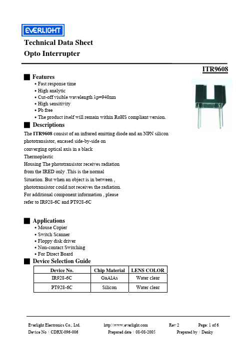
ITR9608中文资料
EVERLIGHT corporation . Please don't reproduce or cause anyone to reproduce them without EVERLIGHT's consent 6.When using this product , please observe the absolute maximum ratings and the instructions for use outlined in these specification sheets. EVERIGHT assumes no responsibility for any damage resulting from use of the product which does not comply with the absolute maximum ratings and the instructions included in these specification sheets.
100 C
10
1
0.1
0.01
0.5
1
1.5
3
2
Fig.6 Collector Current vs.
Collector-Emitter Voltage
14
12
10 8
6
4
2
0
0
1
2
3
4
Everlight Electronics Co., Ltd. Device No:CDRX-096-006
5058中文资料
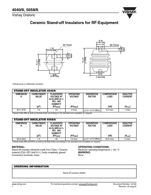
Ceramic Stand-off Insulators for RF-Equipment For technical questions contact: powcap@Document Number: 221801Revision: 29-Aug-024040/6, 5058/6Vishay Draloric• Dimensions in millimeters (inches)Thread holes M8 as well as thread-holes according to US standard are available on request.Thread holes M8 and M10 as well as thread-holes according to US standard are available on request.STAND-OFF INSULATOR 4040/6DIMENSIONHCAPACITANCEVALUE[pF]FLASHOVER VOLTAGE AT 50 Hz AND 60 %REL. AIR HUMIDITY [KV RMS ]OPERATING VOLTAGE[KV RMS ] DISSIPATION FACTORCOMPRESSIVELOAD[kN] REACTIVE CURRENT[A rms ] 40 (1.575)1.6244 max.≤ 0.5 • 10-3[1 MHz]5.0 max.1 max.STAND-OFF INSULATOR 5058/6DIMENSIONHCAPACITANCEVALUE[pF]FLASHOVER VOLTAGE AT 50 Hz AND 60 %REL. AIR HUMIDITY [KV RMS ]OPERATING VOLTAGE[KV RMS ] DISSIPATION FACTORCOMPRESSIVELOAD[kN] REACTIVE CURRENT[A rms ] 58 (2.283)1.03512 max.≤ 0.5 • 10-3[1 MHz]20.0 max.3 max.MATERIAL:Stand-off insulator elements made from Class 1 Ceramic material (C221-IEC 60672-3 ), body completely glazed. Connection terminals: brassOPERATING CONDITIONS:Maximum operating temperature + 100 °CMARKING:NoneORDERING INFORMATIONStand-off insulator 5058/6元器件交易网Document Number: 91000Revision: 18-Jul-081DisclaimerLegal Disclaimer NoticeVishayAll product specifications and data are subject to change without notice.Vishay Intertechnology, Inc., its affiliates, agents, and employees, and all persons acting on its or their behalf (collectively, “Vishay”), disclaim any and all liability for any errors, inaccuracies or incompleteness contained herein or in any other disclosure relating to any product.Vishay disclaims any and all liability arising out of the use or application of any product described herein or of any information provided herein to the maximum extent permitted by law. The product specifications do not expand or otherwise modify Vishay’s terms and conditions of purchase, including but not limited to the warranty expressed therein, which apply to these products.No license, express or implied, by estoppel or otherwise, to any intellectual property rights is granted by this document or by any conduct of Vishay.The products shown herein are not designed for use in medical, life-saving, or life-sustaining applications unless otherwise expressly indicated. Customers using or selling Vishay products not expressly indicated for use in such applications do so entirely at their own risk and agree to fully indemnify Vishay for any damages arising or resulting from such use or sale. Please contact authorized Vishay personnel to obtain written terms and conditions regarding products designed for such applications.Product names and markings noted herein may be trademarks of their respective owners.元器件交易网。
东芝芯片资料
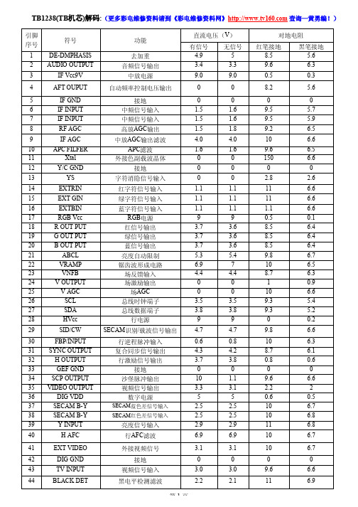
0 900Ω 600Ω 19.5K 15K 13K 19K
LA7833引脚功能
引脚
1 2 3 4 4 6 7
功能
接地端 场输出 自举升压电源端 场激励输入 负反馈输入及相位补偿 电源端 场逆程脉冲输出
直流电压
0V 13.6V 25.5V 0.8V 0.8V 26V 1.4V
纹波滤波电路引脚 第二伴音中频输出 调频直流反馈滤波电路引脚
电压
1.8V 0V 1.3V
+2.5V
+5V 2.45V 2.45V
1V 6.4V 0V 0V 2.3V 1.6V 0V +5V 3.6V 4.3V 0V 8V 8.8V 3.5V 5.6V 3.4V 3.5V
RXIK档对地电阻(黑表笔接地)
场AGC 总线时钟端子 总线数据端子
行电源 SECAM识别/载波信号输出
行逆程脉冲输入 复合同步信号输出 行激励信号输出
接地 沙堡脉冲输出 视频信号输出
数字电源
SECAM蓝色差信号输入 SECAM红色差信号输入
亮度信号输入 行AFC滤波
外接视频信号
接地 视频信Leabharlann 输入黑电平检测滤波直流电压(V)
有信号 4.9
800Ω 0
12.5K
12.8K
6K 13K 13K 13K 12.8K 13.2K
0 12.8K 13K 11.5K
1K 12.5K 12K
0 900Ω 600Ω 12.5K 12.2K 11.5K 12K
红笔接地 R×1K档
800Ω 0
19K
27K
5.5K 20K 20K 18K 28K 28K
eta9098芯片手册
eta9098芯片手册引言:ETA9098芯片是一款高性能的集成电路芯片,广泛应用于各种电子设备中。
本文将详细介绍ETA9098芯片的特性、功能以及应用领域,以帮助读者更好地了解和应用该芯片。
正文内容:1. ETA9098芯片的特性1.1 高性能处理能力1.2 低功耗设计1.3 多功能接口1.4 强大的安全性能1.5 可扩展性强2. ETA9098芯片的功能2.1 数据处理功能2.2 通信功能2.3 传感器接口功能2.4 存储功能2.5 电源管理功能3. ETA9098芯片在智能手机中的应用3.1 高性能处理能力支持流畅的应用使用3.2 多功能接口实现各种外设的连接3.3 强大的安全性能保护用户隐私3.4 低功耗设计延长手机续航时间3.5 可扩展性强满足不同用户需求4. ETA9098芯片在物联网设备中的应用4.1 数据处理功能支持物联网设备的智能化4.2 通信功能实现物联网设备之间的互联互通4.3 传感器接口功能支持物联网设备的感知能力4.4 存储功能实现物联网设备数据的存储与管理4.5 电源管理功能延长物联网设备的使用寿命5. ETA9098芯片在汽车电子中的应用5.1 高性能处理能力支持汽车电子系统的复杂计算5.2 多功能接口连接各种汽车外设5.3 强大的安全性能保护汽车系统的安全5.4 低功耗设计减少能源消耗5.5 可扩展性强满足汽车电子系统的不断升级需求总结:ETA9098芯片作为一款高性能的集成电路芯片,在智能手机、物联网设备和汽车电子等领域都有着广泛的应用。
其特性包括高性能处理能力、低功耗设计、多功能接口、强大的安全性能以及可扩展性强。
其功能包括数据处理、通信、传感器接口、存储和电源管理等。
在不同应用领域中,ETA9098芯片都发挥着重要的作用,提升了设备的性能和功能,满足了用户的需求。
随着技术的不断发展,ETA9098芯片将继续在各个领域中发挥重要作用,推动电子设备的进一步发展。
dm9000中文芯片手册
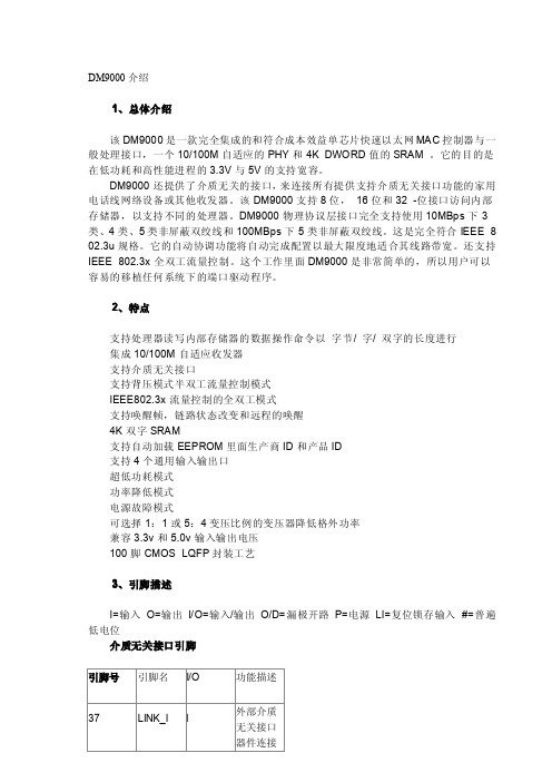
各 种其 他 功能 引 脚
16~19 TEST1~4 I
48
TEST5 I
68~69 GPIO0~3 I/O
78
LINK_O O
79
WAKEUP O
工作模式
Test1~4(1, 1,0,0)正常 工作状态
必须接地
通用 I/O 端 口
通用 端口控制 寄存器和 通用端口 寄存器能 编程该系 列引脚
GPIO0 默 认输出为 高来关闭 物理层和 其他外部 介质无关 器件
外部介质 无关接口 接收错误
外部介质 无关接口 接收时钟
外部介质 无关接口 发送时钟
外部介质 无关接口 发送数据 低 4 位输
出
TXD[2:0] 决定内部 存储空间 基址:TXD [2:0]) * 10H + 300H
外部介质
无关接口
54
MDIO I/O
串行数据
通信
57
MDC O
外部介质 无关串行 数据通信 口时钟,且 与中断引 脚有关
带隙引脚
27
AVDD P
带隙与电 源保护环
28
AVDD P
接收端口 电源
29
RXI+ I
物理层接 收端的正 极
30
RXI-
I
物理层接 收端的负 极
31
AGND P
接收端口 地
32
AGND P
发送端口 地
33
TXO+ O
物理层发 送端口正 极
34
TXO- O
发送端口 负极
35
AVDD P
物理层发 送端口负 极
WAKEUP EEDO 总 线宽度
00 16 位
Mstar MST6i98机芯介绍
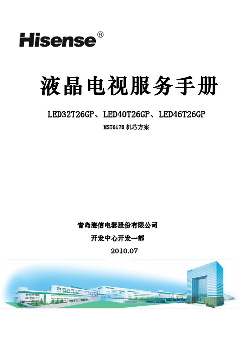
R液晶电视服务手册 LED32T26GP、LED40T26GP、LED46T26GPMST6i78机芯方案青岛海信电器股份有限公司开发中心开发一部2010.07目 录LED32T26GP、LED40T26GP、LED46T26GP (4)一、产品介绍 (4)(一)、产品外观介绍 (4)(二)、产品功能规格、特点介绍 (5)(三)、产品差异介绍 (6)二、方案概述 (6)三、电路框图构架 (6)四、电源分配 (7)五、原理说明 (8)1、电源部分---系统3.3Vstb (8)2、电源部分---系统+5V (8)3、电源部分---系统3.3V:33V_Normal (8)4、电源部分---系统2.5V:+2.5V_Normal (9)5、电源部分---6i78 核电:VCC1.2V (9)6、电源部分---液晶屏TCON供电:VCC-Panel (9)7、电源部分---USB供电:5V_USB1 (10)8、控制部分---待机控制电路:STANDBY (10)9、控制部分---背光ON/OFF和调光电路: (11)10、存储部分---Mboot FLASH (11)11、存储部分---NAND FLASH (12)12、存储部分---EEPROM (12)13、按键电路---支持触摸按键和机械按键 (13)14、遥控电路---支持灯效控制、光感 (13)15、DDR电路---DDR3_H5TQ1G63BFR-12C (14)16、接口部分---HDMI接口 (15)17、接口部分---HDMI EDID 和HOTPLUG (15)18、接口部分---高清接口 (15)19、接口部分---AV接口 (16)20、接口部分---VGA接口 (17)21、接口部分---AV输出接口 (17)22、接口部分---AV输出接口—音频输出 (17)23、接口部分---同轴输出电路 (18)24、接口部分---耳机输出电路 (18)25、开关机静音电路 (19)26、数字供放电路 (20)27、数字功放电路—重低音电路 (20)28、tuner 部分---33V供电 (21)29、tuner 部分---5V-IF (21)30、tuner 部分---tuner (21)31、tuner 部分---tuner预中放电路 (22)32、tuner 部分---声表电路 (23)33、6M20 部分---电源 (23)34、6M20 部分---LVDS部分 (24)六、产品爆炸图及明细 (25)1、LED32T26GP: (25)2、LED40T26GP: (27)3、LED46T26GP: (29)七、主板及电源板图: (31)主板实物图 (31)电源板实物图 (32)电源板电路图 (33)八、软件升级方法 (34)液晶电视服务手册----LED32T26GP、LED40T26GP、LED46T26GP一、产品介绍:(一)产品外观介绍:1、LED32T26GP、LED40T26GP、LED46T26GP外观:2、外观实景图:(因拍摄技术有限,图片仅供参考)(二)产品功能规格、特点介绍:1、技术参数:2、各端子电平特性:(三)产品差异介绍:1、LED32T26GP是在LED32T29P基础上更换前壳;2、LED40T26GP是在LED40T28PKV基础上去掉重低音端子并更换前壳;3、LED46T26GP是在LED40T26GP上只更换屏。
LTC2950IDDB-1#TRMPBF;LTC2950ITS8-2#TRMPBF;LTC2950IDDB-2#TRMPBF;中文规格书,Datasheet资料
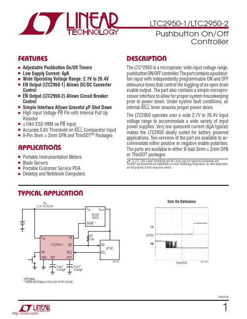
Electrical Characteristics The l denotes the specifications which apply over the full operating
temperature range, otherwise specifications are at TA = 25°C. VIN = 2.7V to 26.4V, unless otherwise noted. (Note 2)
LTC2950-1/LTC2950-2
Pushbutton On/Off Controller
Features
n Adjustable Pushbutton On/Off Timers n Low Supply Current: 6µA n Wide Operating Voltage Range: 2.7V to 26.4V n EN Output (LTC2950-1) Allows DC/DC Converter
Operating Temperature Range LTC2950C-1.............................................. 0°C to 70°C LTC2950C-2.............................................. 0°C to 70°C LTC2950I-1...........................................–40°C to 85°C LTC2950I-2...........................................–40°C to 85°C
Consult LTC Marketing for parts specified with wider operating temperature ranges. Consult LTC Marketing for information on lead based finish parts.
mt8985apr中文资料_数据手册_IC数据表

1Features•256 x 256 channel non-blocking switch •Programmable frame integrity for wideband channels•Automatic identification of ST-BUS/GCI interface backplanes•Per channel tristate control •Patented message mode•Non-multiplexed microprocessor interface •Single +5 volt supply•Available in DIP-40, PLCC-44 and QFP-44 packages•Pin compatible with MT8980 deviceApplications•Medium size digital switch matrices•Hyperchannel switching (e.g., ISDN H0)•ST-BUS/MVIP ™ interface functions •Serial bus control and monitoring•Centralized voice processing systems •Data multiplexerDescriptionThe MT8985 Enhanced Digital Switch device is an upgraded version of the popular MT8980D DigitalSwitch (DX). It is pin compatible with the MT8980D and retains all of the MT8980D's functionality. This VLSI device is designed for switching PCM-encoded voice or data, under microprocessor control, in digital exchanges, PBXs and any ST-BUS/MVIP environment. It provides simultaneous connections for up to 256 64kb/s channels. Each of the eight serial inputs and outputs consist of 32 64 kbit/s channels multiplexed to form a 2048 kbit/s stream. As the main function in switching applications, the device provides per-channel selection between variable or constant throughput delays. The constant throughput delay feature allows grouped channels such as ISDN H0 to be switched through the device maintaining its sequence integrity. The MT8985 is ideal for medium sized mixed voice/data switch and voice processing applications.September 2005Ordering InformationMT8985AE 40 Pin PDIP Tubes MT8985AP 44 Pin PLCC Tubes MT8985AL 44 Pin MQFP Trays MT8985APR 44 Pin PLCC Tape & Reel MT8985AP144 Pin PLCC*TubesMT8985APR144 Pin PLCC*Tape & Reel MT8985AE140 Pin PDIP*Tubes MT8985AL144 Pin MQFP*Trays*Pb Free Matte Tin-40°C to +85°CCMOS ST-BUS TM FamilyMT8985Enhanced Digital SwitchData SheetFigure 1 - Functional Block Diagramhttps://MT8985Data SheetChanges SummaryThe following table captures the changes from the May 2005 issue.Figure 2 - Pin ConnectionsPage ItemChange7Figure 3 - “Address Memory Map“•corrected Address Memory MapDTA STi0STi1STi2STi3STi4STi5STi6STi7VDD F0i C4i A0A1A2A3A4A5DS CSTo ODE STo0STo1STo2STo3STo4STo5STo6STo7VSS D0D1D2D3D4D5D6D7CS1654324443424140789101112131415163938373635343332313023181920212224252627281729STi3STi4STi5STi6STi7VDD F0i C4i A0A1A2STo3STo4STo5STo6STo7VSS D0D1D2D3D4N C S T i 1D T A O D E S T o 1N CS T i 2S T i 0C S T o S T o 0S T o 2N C A 4D S C S D 6N CA 3A 5R /W D 740 PIN PLASTIC DIP44 PIN PLCC2345678910111213141516171819201R/W4039383736353433323130292827262524232221D 5394443424140383736353412345678910333231302928272625241712131415161819202122112344 PIN QFPSTi3STi4STi5STi6STi7VDD F0i C4i A0A1A2N C A 4D S C S D 6N CA 3A 5R /W D 7D 5STo3STo4STo5STo6STo7VSS D0D1D2D3D4N C S T i 1D T A O D E S T o 1N CS T i 2S T i 0C S T o S T o 0S T o 2https://MT8985Data SheetPin DescriptionPin #Name Description40 DIP44PLCC 44QFP1240DTAData Acknowledgement (Open Drain Output). This active low output indicates that a data bus transfer is complete. A pull-up resistor is required at this output.2-93-57-1141-431-5STi0-STi7ST-BUS Input 0 to 7 (Inputs). Serial data input streams. These streams have 32 channels at data rates of 2.048 Mbit/s.10126V DD +5 Volt Power Supply rail.11137F0iFrame Pulse (Input): This input accepts and automatically identifies framesynchronization signals formatted according to different backplane specifications such as ST-BUS and GCI.12148C4iClock (Input). 4.096 MHz serial clock for shifting data in and out of the data streams.13-1815-1719-219-1113-15A0-A5Address 0 to 5 (Inputs). These lines provide the address to MT8985 internalregisters.192216DSData Strobe (Input). This is the input for the active high data strobe on themicroprocessor interface. This input operates with CS to enable the internal read and write generation.202317R/W Read/Write (Input). This input controls the direction of the data bus lines (D0-D7) during a microprocessor access. 212418CSChip Select (Input). Active low input enabling a microprocessor read or write ofcontrol register or internal memories.22-2925-2729-3319-2123-27D7-D0Data Bus 7 to 0 (Bidirectional). These pins provide microprocessor access to datain the internal control register, connect memory high, connect memory low and datamemory.303428V SSGround Rail.31-3835-3941-4329-3335-37STo7-STo0ST-BUS Outputs 7 to 0 (Three-state Outputs). Serial data output streams. Thesestreams are composed of 32 channels at data rates of 2.048 Mbit/s.394438ODE Output Drive Enable (Input). This is an output enable for the STo0 to STo7 serialoutputs. If this input is low STo0-7 are high impedance. If this input is high each channel may still be put into high impedance by software control.40139CSTo Control ST-BUS Output (Output). This output is a 2.048 Mb/s line which contains256 bits per frame. The level of each bit is controlled by the contents of the CSTo bit in the Connect Memory high locations.6, 18,28, 4012,2234,44NCNo Connection.https://MT8985Data SheetFunctional DescriptionWith the integration of voice, video and data services into the same network, there has been an increasing demand for systems which ensure that data at N x 64 Kbit/s rates maintain frame sequence integrity while being transported through time slot interchange circuits. Existing requirements demand time slot interchange devices performing switching with constant throughput delay while guaranteeing minimum delay for voice channels.The MT8985 device provides both functions and allows existing systems based on the MT8980D to be easily upgraded to maintain the data integrity while multiple channel data are transported. The device is designed to switch 64 kbit/s PCM or N x 64 kbit/s data. The MT8985 can provide both frame integrity for data applications and minimum throughput switching delay for voice applications on a per channel basis.By using Zarlink Message mode capability, the microprocessor can access input and output time slots on a per channel basis to control devices such as the Zarlink MT8972, ISDN Transceivers and T1/CEPT trunk interfaces through the ST-BUS interface. Different digital backplanes can be accepted by the MT8985 device without user's intervention. The MT8985 device provides an internal circuit that automatically identifies the polarity and format of frame synchronization input signals compatible to ST-BUS and GCI interfaces.Device OperationA functional block diagram of the MT8985 device is shown in Figure 1. The serial ST-BUS streams operate continuously at 2.048 Mb/s and are arranged in 125 µs wide frames each containing 32 8-bit channels. Eight input (STi0-7) and eight output (STo0-7) serial streams are provided in the MT8985 device allowing a complete 256 x 256 channel non-blocking switch matrix to be constructed. The serial interface clock for the device is 4.096 MHz, as required in ST-BUS and GCI specifications.https://Data MemoryThe received serial data is converted to parallel format by the on-chip serial to parallel converters and stored sequentially in a 256-position Data Memory. The sequential addressing of the Data Memory is generated by an internal counter that is reset by the input 8 kHz frame pulse (F0i) marking the frame boundaries of the incoming serial data streams.Depending on the type of information to be switched, the MT8985 device can be programmed to perform time slot interchange functions with different throughput delay capabilities on a per-channel basis. For voice applications, the variable delay mode can be selected ensuring minimum throughput delay between input and output data. In multiple or grouped channel data applications, the constant delay mode can be selected maintaining the integrity of the information through the switch.Data to be output on the serial streams may come from two sources: Data Memory or Connect Memory. Locations in the Connect Memory, which is split into HIGH and LOW parts, are associated with particular ST-BUS output streams. When a channel is due to be transmitted on an ST-BUS output, the data for the channel can either be switched from an ST-BUS input (connection mode) or it can be originated from the microprocessor (message mode). If a channel is configured in connection mode, the source of the output data is the Data Memory. If a channel is configured in message mode, the source of the output data is the Connect Memory Low. Data destined for a particular channel on the serial output stream is read from the Data or Connect Memory Low during the previous channel time slot. This allows enough time for memory access and internal parallel to serial conversion.Connection and Message ModesIn connection mode, the addresses of input source for all output channels are stored in the Connect memory Low. The Connect Memory Low locations are mapped to each location corresponding to an output 64 kb/s channel. The contents of the Data memory at the selected address are then transferred to the parallel to serial converters. By having the output channel to specify the input channel through the connect memory, the user can route the same input channel to several output channels, allowing broadcasting facility in the switch.MT8985Data SheetIn message mode the CPU writes data to the Connect Memory Low locations which correspond to the output link and channel number. The contents of the Connect Memory Low are transferred to the parallel to serial converter one channel before it is to be output. The Connect Memory Low data is transmitted each frame to the output until it is changed by the CPU.The per-channel functions available in the MT8985 are controlled by the Connect Memory High bits, which determine whether individual output channels are selected into specific conditions such as: message or connection mode, variable or constant throughput delay modes, output drivers enabled or in three-state condition. In addition, the Connect Memory High provides one bit to allow the user to control the state of the CSTo output pin.If an output channel is set to three-state condition, the TDM serial stream output will be placed in high impedance during that channel time. In addition to the per-channel three-state control, all channels on the TDM outputs can be placed in high impedance at one time by pulling the ODE input pin in LOW. This overrides the individual per-channel programming on the Connect Memory High bits.The Connect Memory data is received via the Microprocessor Interface at D0-D7 lines. The addressing of the MT8985 internal registers, Data and Connect memories is performed through address input pins and some bits of the device's Control register. The higher order address bits come from the Control register, which may be written or read through the microprocessor interface. The lower order address bits come directly from the external address line inputs. For details on the device addressing, see Software Control and Control register description.Serial Interface TimingThe MT8985 master clock (C4i) is a 4.096 MHz allowing serial data link configuration at 2.048 Mb/s to be implemented. The MT8985 frame synchronization pulse can be formatted according to ST-BUS or GCI interface specifications; i.e., the frame pulse can be active in HIGH (GCI) or LOW (ST-BUS). The MT8985 device https://automatically detects the presence of an input frame pulse and identifies the type of backplane present on the serial interface. Upon determining the correct interface connected to the serial port, the internal timing unit establishes the appropriate serial data bit transmit and sampling edges. In ST-BUS mode, every second falling edge of the 4.096 MHz clock marks a bit boundary and the input data is clocked in by the rising edge, three quarters of the way into the bit cell. In GCI mode, every second rising edge of the 4.096 MHz clock marks the bit boundary while data sampling is performed during the falling edge, at three quarters of the bit boundaries.Delay through the MT8985The transfer of information from the input serial streams to the output serial streams results in a delay through the MT8985 device. The delay through the MT8985 device varies according to the mode selected in the V/C bit of the connect memory high.Variable Delay ModeThe delay in this mode is dependent only on the combination of source and destination channels and it is not dependent on the input and output streams. The minimum delay achievable in the MT8985 device is 3 time slots. In the MT8985 device, the information that is to be output in the same channel position as the information is input (position n), relative to frame pulse, will be output in the following frame (channel n, frame n+1). The same occurs if the input channel has to be output in the two channels succeeding (n+1 and n+2) the channel position as the information is input.The information switched to the third timeslot after the input has entered the device (for instance, input channel 0 to output channel 3 or input channel 30 to output channel 1), is always output three channels later.Any switching configuration that provides three or more timeslots between input and output channels, will have a throughput delay equal to the difference between the output and input channels; i.e., the throughput delay will be less than one frame. Table 1 shows the possible delays for the MT8985 device in Variable Delay mode:MT8985Data SheetConstant Delay ModeIn this mode frame integrity is maintained in all switching configurations by making use of a multiple Data-Memory buffer technique where input channels written in any of the buffers during frame N will be read out during frame N+2. In the MT8985, the minimum throughput delay achievable in Constant Delay mode will be 32 time slots; for example, when input time slot 32 (channel 31) is switched to output time slot 1 (channel 0). Likewise, the maximum delay is achieved when the first time slot in a frame (channel 0) is switched to the last time slot in the frame (channel 31), resulting in 94 time slots of delay.To summarize, any input time slot from input frame N will be always switched to the destination time slot on output frame N+2. In Constant Delay mode, the device throughput delay is calculated according to the following formula:DELAY = [32 + (32 - IN) + (OUT - 1)]; (expressed in number of time slots)Where:IN is the number of the input time slot (from 1 to 32).OUT is the number of the output time slot (from 1 to 32).Microprocessor PortThe MT8985 microprocessor port has pin compatibility with Zarlink MT8980 Digital Switch device providing a non-multiplexed bus architecture. The parallel port consists of an 8 bit parallel data bus (D0-D7), six address input lines (A0-A5) and four control lines (CS, DS, R/W and DTA). This parallel microport allows the access to the Control registers, Connection Memory High, Connection Memory Low and the Data Memory. All locations are read/written except for the data memory which can be read only.Accesses from the microport to the connection memory and the data memory are multiplexed with accesses from the input and output TDM ports. This can cause variable Data Acknowledge delays (DTA). In the MT8985 device,the DTA output provides a maximum acknowledgement delay of 800 ns for read/write operations in the Connection Memory. However, for operations in the Data Memory (Message Mode), the maximum acknowledgement delay can be 1220 ns.Input ChannelOutput Channel Throughput Delay n m=n, n+1 or n+2m-n + 32 timeslotsnm>n+2m-n time slotsn m<n 32-(n-m) time slotshttps://MT8985Data SheetFigure 3 - Address Memory MapNote: "x" Don’t careSoftware ControlThe address lines on the microprocessor interface give access to the MT8985 internal registers and memories. If the A5,A1,A0 address line inputs are LOW, then the MT8985 Internal Control Register is addressed (see Figure 3).If A5 input line is HIGH, then the remaining address input lines are used to select Memory subsections of 32locations corresponding to the number of channels per input or output stream. As explained in the Control register description, the address input lines and the Stream Address bits (STA) of the Control register give the user the capability of selecting all positions of the MT8985 Data and Connect memories.The data in the Control register consists of Split memory and Message mode bits, Memory select and Stream Address bits (see Figure 4). The memory select bits allow the Connect Memory HIGH or LOW or the Data Memory to be chosen, and the Stream Address bits define an internal memory subsections corresponding to input or output ST-BUS streams. Bit 7 (Split Memory) of the Control register allows split memory operation whereby reads are from the Data memory and writes are to the Connect Memory LOW.The Message Enable bit (bit 6) places every output channel on every output stream in message mode; i.e., the contents of the Connect Memory LOW (CML) are output on the ST-BUS output streams once every frame unless the ODE input pin is LOW. If ME bit is HIGH, then the MT8985 behaves as if bits 2 (Message Channel) and 0(Output Enable) of every Connect Memory HIGH (CMH) locations were set to HIGH, regardless of the actual value.If ME bit is LOW, then bit 2 and 0 of each Connect Memory HIGH location operates normally. In this case, if bit 2 of the CMH is HIGH, the associated ST-BUS output channel is in Message mode. If bit 2 of the CMH is LOW, then the contents of the CML define the source information (stream and channel) of the time slot that is to be switched to an output.If the ODE input pin is LOW, then all serial outputs are high-impedance. If ODE is HIGH, then bit 0 (Output Enable)of the CMH location enables (if HIGH) or disables (if LOW) the output drivers for the corresponding individual ST-BUS output stream and channel.The contents of bit 1 (CSTo) of each Connection Memory High location (see Figure 5) is output on CSTo pin once every frame. The CSTo pin is a 2048 Mbit/s output which carries 256 bits. If CSTo bit is set HIGH, the corresponding bit on CSTo output is transmitted in HIGH. If CSTo bit is LOW, the corresponding bit on the CSTo output is transmitted in LOW. The contents of the 256 CSTo bits of the CMH are transmitted sequentially on to the CSTo output pin and are synchronous to the ST-BUS streams. To allow for delay in any external control circuitry the contents of the CSTo bit is output one channel before the corresponding channel on the ST-BUS streams. For example, the contents of CSTo bit in position 0 (ST0, CH0) of the CMH, is transmitted synchronously with ST-BUS channel 31, bit 7. The contents of CSTo bit in position 32 (ST1, CH0) of the CMH is transmitted during ST-BUS channel 31 bit 6. Bit V/C (Variable/Constant Delay) on the Connect Memory High locations allow per-channel selection between Variable and Constant throughput delay capabilities.A5A4A3A2A1A0LOCATION 011111111000•••••1000•••••1000•••••1000•••••1001•••••1Control Register Channel 0Channel 1•••••Channel 31https://MT8985Data SheetFigure 4 - Control Register Bitsx = Don’t careInitialization of the MT8985On initialization or power up, the contents of the Connection Memory High can be in any state. This is a potentially hazardous condition when multiple MT8985 ST-BUS outputs are tied together to form matrices, as these outputs may conflict. The ODE pin should be held low on power up to keep all outputs in the high impedance condition.BIT NAME DESCRIPTION7SM Split Memory. When 1, all subsequent reads are from the Data Memory and writes are to theConnection Memory Low, except when the Control Register is accessed again. The Memory Select bits need to be set to specify the memory for the operations. When 0, the Memory Select bits specify the memory for subsequent operations. In either case, the Stream Address Bits select the subsection of the memory which is made available.6MEMessage Enable. When 1, the contents of the Connection Memory Low are output on the Serial Output streams except when in High Impedance. When 0, the Connection Memory bits for each channel determine what is output.4-3MS1-MS0Memory Select Bits. The memory select bits operate as follows:0-0 - Not to be used0-1 - Data Memory (read only from the CPU)1-0 - Connection Memory Low 1-1 - Connection Memory High2-0STA2-0Stream Address Bits 2-0. The number expressed in binary notation on these bits refers to the input or output ST-BUS stream which corresponds to the subsection of memory made accessible for subsequent operations.SMMEXMS1MS0STA2STA1STA076543210https://MT8985Data SheetFigure 5 - Connection Memory High Bitsx = Don’t careFigure 6 - Connection Memory Low BitsDuring the microprocessor initialization routine, the microprocessor should program the desired active paths through the matrices, and put all other channels into the high impedance state. Care should be taken that no two connected ST-BUS outputs drive the bus simultaneously. When this process is complete, the microprocessor controlling the matrices can bring the ODE signal high to relinquish high impedance state control to the CMH b 0s.BIT NAME DESCRIPTION6V/C Variable/Constant Throughput Delay Mode. This bit is used to select between Variable (LOW) and Constant Delay (HIGH) modes on a per-channel basis.2MCMessage Channel. When 1, the contents of the corresponding location in Connection Memory Low are output on the corresponding channel and stream. When 0, the contents of the programmed location in Connection Memory Low act as an address for the Data Memory and so determine the source of the connection to the location’s channel and stream.1CSTo CSTo Bit. This bit drives a bit time on the CSTo output pin.OEOutput Enable. This bit enables the output drivers on a per-channel basis. This allows individual channels on individual streams to be made high-impedance, allowing switch matrices to be constructed. A HIGH enables the driver and a LOW disables it.BIT NAME DESCRIPTION7-5SAB2-0*Source Stream Address bits. These three bits are used to select eight source streams for the connection. Bit 7 of each word is the most significant bit.4-0*CAB4-0*Source Channel Address bits 0-4. These five bits are used to select 32 different source channels for the connection (The ST-BUS stream where the channel is present is defined by bits SAB2-0). Bit 4 is the most significant bit.*If bit 2 of the corresponding Connection High location is 1 or if bit 6 of the Control Register is 1, then these entire 8 bits are output on the channel and stream associated with this location. Otherwise, the bits are used as indicated to define the source of the connection which is output on the channel and stream associated with this location.XV/CXXXMCCSToOE76543210SAB2SAB1SAB0CAB4CAB3CAB2CAB1CAB07654321https://MT8985Data Sheet ApplicationsTypical Exchange, PBX or MultiplexerFigure 7 shows a typical implementation of line cards being interconnected through a central routing matrix that can scale up in channel capacity to accommodate different number of ports depending on the application. In a configuration where the switched services utilize concatenated or grouped time slots to carry voice, data and video (channels of 128, 256 Kb/s, ISDN H0 and others), the central routing matrix has to guarantee constant throughput delay to maintain the sequence integrity between input and output channels. Figure 7 shows an example where the MT8985 device guarantees data integrity when data flows from the T1/E1 to the S/U interface links and vice-versa. Modern technologies available today such as Frame Relay network using dedicated fractional T1 are one of the key applications for the MT8985 device.Figure 7 - Typical Exchange, PBX or Multiplexer ConfigurationMT8985Data SheetLow Latency Isochronous NetworkIn today's local working group environment, there is an increasing demand for solutions on interconnection of desktop and telephone systems so that mixed voice, data and video services can be grouped together in a reliable https://network allowing the deployment of multimedia services. Existing multimedia applications require a network with predictable data transfer delays that can be implemented at a reasonable cost. The Low Latency Isochronous Network is one of the alternatives that system designers have chosen to accommodate this requirement (see Figure 8a). This network can be implemented using existing TDM transmission media devices such as ISDN Basic (S or U) and Primary rates trunks (T1 and CEPT) to transport mixed voice and data signals in grouped time slots; for example, 2B channels in case of ISDN S or U interfaces or up to 32 channels in case of a CEPT link.Figure 8b shows a more detailed configuration whereby several PCs are connected to form an Isochronous network. Several services can be interconnected within a single PC chassis through the standardized Multi Vendor Integration Protocol (MVIP). Such an interface allows the distribution and interconnection of services like voice mail, integrated voice response, voice recognition, LAN gateways, key systems, fax servers, video cards, etc.The information being exchanged between cards through the MVIP interface on every computer as well as between computers through T1 or CEPT links is, in general, of mixed type where 64Kb/s and N*64Kb/s channels are grouped together. When such a mixed type of data is transferred between cards within one chassis or from one computer to another, the sequence integrity of the concatenated channels has to be maintained. The MT8985 device suits this application and can be used to form a complete non-blocking switch matrix of 512 channels (see Figure 9). This allows 8 pairs of ST-BUS streams to be dedicated to the MVIP side whereas the remaining 8 pairs are used for local ancillary functions in typical dual T1/E1 interface applications (Figure 10).Another application of the MT8985 in an MVIP environment is to build an ISDN S-interface card (Figure 11). In this card, 7 pairs of ST-BUS streams are connected to the MVIP interface while the remaining pair is reserved for the interconnection of Zarlink MT8930 (SNIC), MT8992 (H-PHONE) and the MVIP interface.MT8985Data Sheet To Video, Data,MT8985Data SheetFigure 9 - 512-Channel Switch Array8 Input Streams From MVIP8 Input On-Board ST-BUS Streams8 Output Streams to MVIP8 Output On-Board ST-BUS StreamsMVIP DirectionMVIP EnableMT8985 #1CSToMT8985 #2CSToMT8985#3MT8985#4https://MT8985Data SheetFigure 10 - Dual T1/E1 Card Functional Block DiagramFDL HDLC MT8952B T1/E1MH89760Bor MH89790B HDLC MT8952BANALOG D-PHONE MT8992/93SWITCH MT8985SWITCH MT8985SWITCH MT8985SWITCH MT8985DPLL MT8941PC INTERFACEMVIP HEADERMVIP STo0-7MVIP STi0-7FDL HDLC MT8952BT1/E1MH89760Bor MH89790B HDLC MT8952B512 Channel Switch Matrixhttps://MT8985Data SheetFigure 11 - S-Access Card Functional Block DiagramMVIP HEADERSWITCH MATRIX SINTERFACEHDLCDIGITAL PHONEDPLL DTMF RECEIVER PC INTERFACEHDLCSTi7-1STo7-1STi0STo0MT8930BMT8941MT8992/93MT8870MVIP STi1-7MVIP STo1-7MT8985https://。
12位2路8脚DA芯片
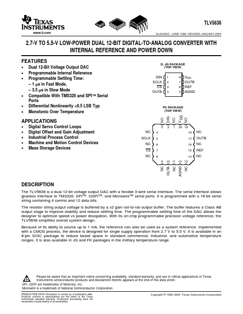
DISSIPATION RATING TABLE
PACKAGE
D FK JG
TA≤ 25°C POWER RATING
635 mW
1375 mW
1050 mW
DERATING FACTOR ABOVE TA= 25°C(1)
5.08 mW/°C
11.00 mW/°C
8.40 mW/°C
TA= 70°C POWER RATING
407 mW
880 mW
672 mW
TA = 85°C POWER RATING
330 mW
715 mW
546 mW
TA = 125°C POWER RATING
127 mW
275 mW
210 mW
(1) This is the inverse of the traditional Junction-to-Ambient thermal Resistance (RθJA). Thermal Resistances are not production tested and are for informational purposes only.
D, JG PACKAGE (TOP VIEW)
DIN 1 SCLK 2
CS 3 OUTA 4
8 VDD 7 OUTB 6 REF 5 AGND
FK PACKAGE (TOP VIEW)
NC DIN NC VDD NC
NC SCLK
NC CS NC
3 2 1 20 19
4
18
5
17
6
16
7
15
8
14ቤተ መጻሕፍቲ ባይዱ
Please be aware that an important notice concerning availability, standard warranty, and use in critical applications of Texas Instruments semiconductor products and disclaimers thereto appears at the end of this data sheet.
AOT9608中文资料
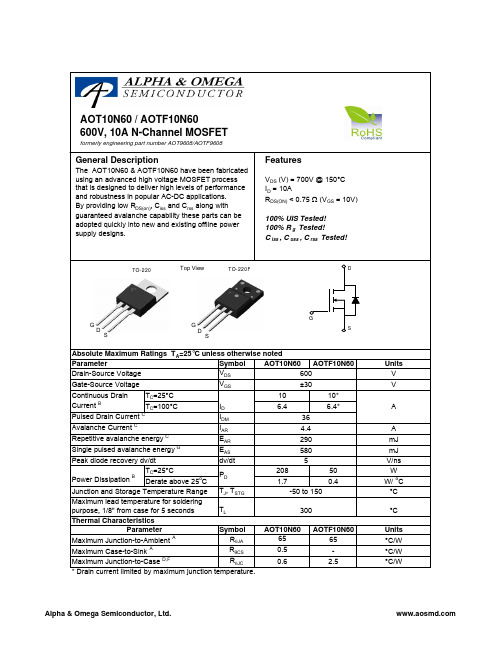
Continuous DrainParameter T =25°C Gate-Source Voltage Drain-Source Voltage Absolute Maximum Ratings T =25°C unless otherwise notedAOT10N60 / AOTF10N60DSDSSymbolMin Typ Max Units600V 700V BV DSS /∆T J 0.65V/ oC 110I GSS ±100nA V GS(th)345V R DS(ON)0.60.75Ωg FS 15S V SD 0.731V I S 10A I SM36A C iss 110013201600pF C oss 105130160pF C rss 7.59.311pF R g33.86ΩQ g 31.140nC Q gs 6.410nC Q gd 14.420nC t D(on)2835ns t r 6680ns t D(off)7695ns t f 6480ns t rr 290350ns Q rr3.94.7µC4.4THIS PRODUCT HAS BEEN DESIGNED AND QUALIFIED FOR THE CONSUMER MARKET. APPLICATIONS OR USES AS CRITICAL COMPONENTS IN LIFE SUPPORT DEVICES OR SYSTEMS ARE NOT AUTHORIZED. AOS DOES NOT ASSUME ANY LIABILITY ARISING OUT OF SUCH APPLICATIONS OR USES OF ITS PRODUCTS. AOS RESERVES THE RIGHT TO IMPROVE PRODUCT DESIGN,FUNCTIONS AND RELIABILITY WITHOUT NOTICE.V DS =480V, T J =125°C Breakdown Voltage Temperature CoefficientI D =250µA, V GS =0V Gate Threshold VoltageV DS =V GS , I D =250µA V DS =600V, V GS =0V V DS =0V, V GS =±30V Zero Gate Voltage Drain Current Gate-Body leakage current Body Diode Reverse Recovery TimeI D =250µA, V GS =0V, T J =25°C V GS =10V, I D =5A Reverse Transfer Capacitance I F =10A,dI/dt=100A/µs,V DS =100VV GS =0V, V DS =25V, f=1MHz SWITCHING PARAMETERS I DSS µA Maximum Body-Diode Pulsed CurrentElectrical Characteristics (T J =25°C unless otherwise noted)STATIC PARAMETERS Parameter Conditions Static Drain-Source On-Resistance Forward TransconductanceDiode Forward Voltage I S =1A, V GS =0V V DS =40V, I D =5ATurn-On Rise Time Turn-Off DelayTime V GS =10V, V DS =300V, I D =10A, R G =25ΩGate resistanceV GS =0V, V DS =0V, f=1MHzTurn-Off Fall TimeTotal Gate Charge V GS =10V, V DS =480V, I D =10AGate Source Charge Gate Drain Charge BV DSS Drain-Source Breakdown Voltage I D =250µA, V GS =0V, T J =150°C Body Diode Reverse Recovery Charge I F =10A,dI/dt=100A/µs,V DS =100VMaximum Body-Diode Continuous Current Input Capacitance Output Capacitance Turn-On DelayTime DYNAMIC PARAMETERS A: The value of R θJA is measured with the device in a still air environment with T A =25°C.B. The power dissipation P D is based on T J(MAX)=150°C, using junction-to-case thermal resistance, and is more useful in setting the upper dissipation limit for cases where additional heatsinking is used.C: Repetitive rating, pulse width limited by junction temperature T J(MAX)=150°C.D. The R θJA is the sum of the thermal impedence from junction to case R θJC and case to ambient.E. The static characteristics in Figures 1 to 6 are obtained using <300 µs pulses, duty cycle 0.5% max.F. These curves are based on the junction-to-case thermal impedence which is measured with the device mounted to a large heatsink, assuming a maximum junction temperature of T J(MAX)=150°C.G. L=60mH, I AS =4.4A, V DD =50V, R G =25Ω, Starting T J =25°CRev 0. July 2008VdsC ha rgeG ate Charge Test Circuit & W av eformResistiv e Switching Test Circuit & W av eformsVddVdsI dVgsB V I Unclamped Inductive Switching (UIS) Test Circuit & W av eformsARDSS2E = 1/2 LI VddARAR。
电子秤专业语音芯片说明资料
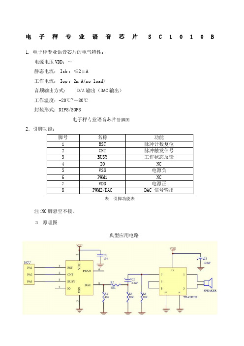
电子秤专业语音芯片S C1010 B
1.电子秤专业语音芯片的电气特性:
电源电压VDD:~
静态电流:Isb :≤2μA
工作电流:Iop :2m A(no load)
音频输出方式:D/A输出(DAC输出)
工作温度:-20℃~+80℃
封装形式:DIP8/SOP8
电子秤专业语音芯片管脚图
2.引脚功能:
脚号名称功能
1RST脉冲计数复位
2CNT脉冲触发信号
3BUSY工作状态反馈
4IO NC
5VSS电源负
6PWM1NC
7VDD电源正
8PWM2/DAC DAC 信号输出
表引脚功能表
注:NC脚悬空不接。
3. 原理图:
典型应用电路
外接功放应用电路
4.时序图:
每次发脉冲触发信号前先发RST复位脉冲计数器大于100us,等待100us后,再发触发信号,发第N个触发信号放第N段语音。
时序图
5.语音内容:
语音内容。
说明书8508A中文手册
8508A配备有多个精密分流器,当电流流过分流器时,可以产生满度200mV的直流电压或交流电压。可以准确测量直流电流和交流电流,交流电流频率范围为1Hz至100kHz。电流源和分流器有两种保护方式:内部电子线路嵌位保护和后面板安置的1.6A保险丝熔断保护。
采用自举电源的斩波稳定放大器为直流电压测量功能提供了低漂移、低噪声、高输入阻抗的优良性能,完善的输入保护电路保证各电压量程都可经受1000V过电压连续冲击。低恒温的齐纳稳压参考源和高精度精密金属箔电阻保证了8508A的直流电压年绝对不确定度优于3.2ppm,温度系数仅为0.3ppm/℃。
交流电压功能保证1Hz至1MHz的平坦频率响应,独特的真有效值(RMS)转换器可准确测量从1%量程至100%量程的交流信号。8508A的点频率方式(Spot)和AC/DC转换(Tfer)方式可进一步提高测量准确度。先在用户选定频率上进行点频率校准,在以后测量中,在点频率±10%频率范围内测量时,可以减少频率响应误差,8508A可以为每个量程选用6个独立的点频率。
从41/2位到81/2位的各种转换位数可提供速度和准确度的最佳选择,从二万分之一到二亿分之一的分辨力为用户提供了最大的便利。
众多的功能
8508A将多种功能组合在一起以适应系统应用和精密测量的需要。直流电压,直流电流,电阻测量,交流电压测量和交直流电流测量,温度测量和IEEE488.2总线接口是标准配置;比率测量和后面板接线柱输入是选件配置。数据处理,数据存贮和测量速度、方式的变化在各个功能都可以实现。
福禄克授权代理商应当只将此种对新的和未使用过的产品的保证延伸到最终使用客户,但无权代表福禄克做出更高的或不同的保证条件。只有从福禄克授权的销售渠道购买的产品或者当购买者已经支付了适当的国际价格时才能获得这种保证支持。当从一个国家购买的产品送到另一个国家进行修理时,福禄克保留向购买者开具修理/更换零件进口费用发票的权利。
8508A中文手册

8508A型参考级81/2位数字多用表操作简要说明福禄克公司北京办事处8508A简明操作手册2有限保证和有限责任每台福禄克的产品在正常使用和维护的情况下保证没有材料和工艺上的缺陷。
产品的保证期为一年,从发运 之日起计算。
零件、产品修理和维护的保证期为90天。
此项保证的对象仅为原始购买者或者福禄克授权代理商的最终使用客户,并且不适用于保险丝、普通电池或者福禄克认为由于意外的或不正常的工作或管理状况而错误使用、经过改动、疏忽管理、受到污染或损坏的产品。
福禄克保证软件将按照其功能技术指标牢靠地工作90天,并已经正确地记录在无缺陷的介质上。
福禄克不保证软件没有错误或工作中无中断。
福禄克授权代理商应当只将此种对新的和未使用过的产品的保证延伸到最终使用客户,但无权代表福禄克 做出更高的或不同的保证条件。
只有从福禄克授权的销售渠道购买的产品或者当购买者已经支付了适当的国际价格时才能获得这种保证支持。
当从一个国家购买的产品送到另一个国家进行修理时,福禄克保留向购买者开具修理/更换零件进口费用发票的权利。
福禄克的保证责任是有限的,对于在保证期之内退回到福禄克授权的维修中心的有缺陷的产品, 福禄克可以选择退还购买款项、免费修理或更换产品。
为获得保修,请与您最近的福禄克授权维修中心联系以得到返修授权信息。
然后将该产品发送到该维修 中心,提供故障说明、并付邮资和保险费(FOB目的地)。
福禄克不承担运输中损坏的风险。
保修之后,该产品将返还给购买者,并付运费(FOB目的地)。
如果福禄克认定故障是由于疏忽管理、错误使用、受到污染、经过改动、意外的或不正常的工作或管理状况,包括因超出产品规定的额定值使用而引起的过电压故障,或者正常的磨损和机械部件的破损而引起,福禄克将提供估计的修理费用并在得到授权之后才开始维修工作。
修理之后,该产品将返还给购买者,并付运费。
购买者则要支付修理费用和返程的运输费用(FOB发运点)。
这种保证是购买者唯一的和专有的补救方法,并且可代替所有其它的保证条件、表述或默许的条款,包 括但不限于任何默许的保证条件或者为某种特定目的的商品性或适应性。
(2021年整理)adc0808中文资料

adc0808中文资料编辑整理:尊敬的读者朋友们:这里是精品文档编辑中心,本文档内容是由我和我的同事精心编辑整理后发布的,发布之前我们对文中内容进行仔细校对,但是难免会有疏漏的地方,但是任然希望(adc0808中文资料)的内容能够给您的工作和学习带来便利。
同时也真诚的希望收到您的建议和反馈,这将是我们进步的源泉,前进的动力。
本文可编辑可修改,如果觉得对您有帮助请收藏以便随时查阅,最后祝您生活愉快业绩进步,以下为adc0808中文资料的全部内容。
11.2。
4 典型的集成ADC芯片为了满足多种需要,目前国内外各半导体器件生产厂家设计并生产出了多种多样的ADC芯片。
仅美国AD公司的ADC产品就有几十个系列、近百种型号之多.从性能上讲,它们有的精度高、速度快,有的则价格低廉.从功能上讲,有的不仅具有A/D转换的基本功能,还包括内部放大器和三态输出锁存器;有的甚至还包括多路开关、采样保持器等,已发展为一个单片的小型数据采集系统。
尽管ADC芯片的品种、型号很多,其内部功能强弱、转换速度快慢、转换精度高低有很大差别,但从用户最关心的外特性看,无论哪种芯片,都必不可少地要包括以下四种基本信号引脚端:模拟信号输入端(单极性或双极性);数字量输出端(并行或串行);转换启动信号输入端;转换结束信号输出端。
除此之外,各种不同型号的芯片可能还会有一些其他各不相同的控制信号端.选用ADC芯片时,除了必须考虑各种技术要求外,通常还需了解芯片以下两方面的特性.(1)数字输出的方式是否有可控三态输出。
有可控三态输出的ADC 芯片允许输出线与微机系统的数据总线直接相连,并在转换结束后利用读数信号RD选通三态门,将转换结果送上总线。
没有可控三态输出(包括内部根本没有输出三态门和虽有三态门、但外部不可控两种情况)的ADC芯片则不允许数据输出线与系统的数据总线直接相连,而必须通过I/O接口与MPU交换信息。
(2)启动转换的控制方式是脉冲控制式还是电平控制式.对脉冲启动转换的ADC芯片,只要在其启动转换引脚上施加一个宽度符合芯片要求的脉冲信号,就能启动转换并自动完成。
selectable 80 or 160 kbps line rate 芯片

selectable 80 or 160 kbps line rate 芯片下载提示:该文档是本店铺精心编制而成的,希望大家下载后,能够帮助大家解决实际问题。
文档下载后可定制修改,请根据实际需要进行调整和使用,谢谢!本店铺为大家提供各种类型的实用资料,如教育随笔、日记赏析、句子摘抄、古诗大全、经典美文、话题作文、工作总结、词语解析、文案摘录、其他资料等等,想了解不同资料格式和写法,敬请关注!Download tips: This document is carefully compiled by this editor. I hope that after you download it, it can help you solve practical problems. The document can be customized and modified after downloading, please adjust and use it according to actual needs, thank you! In addition, this shop provides you with various types of practical materials, such as educational essays, diary appreciation, sentence excerpts, ancient poems, classic articles, topic composition, work summary, word parsing, copy excerpts, other materials and so on, want to know different data formats and writing methods, please pay attention!可选择80或160kbps线速率芯片的应用与发展导言随着信息技术的飞速发展,嵌入式系统在各行各业中的应用越来越广泛。
语音芯片aP89085
341/170/85 sec Voice Length at 6KHz sampling and 4-bit ADPCM compression. Maximum 254 voice groups. Combination of voice blocks to extend playback duration. 7680 table entries are available for voice block combinations. User selectable PCM or ADPCM data compression Three triggering modes are available (controlled by M1 and M0 input pins): Key Trigger Mode (M1=0, M0=0) - S1 ~ S8 to trigger up to 32 voice groups; SBT to trigger up to 254 voice groups sequentially. CPU Parallel Trigger Mode (M1=0, M0=1) – S[8:1] services as 8-bits address to trigger up to 254 voice groups with SBT goes HIGH to strobe the address bits. CPU Serial Command Mode (M1=1, M0=0) – user commands are clocked serially into the chip which enable user to fully control the operation of the chip.
2 5/19/2006
zl40800中文资料_数据手册_IC数据表
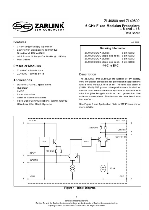
1Features• 3.45V Single Supply Operation•Low Power Dissipation: 190mW typ •Broadband: DC to 6GHz•SSB Phase Noise (–153dBc/Hz @ 10KHz)•Pout 3dBmPrescaler Modulus•ZL40800 – Divide by 8•ZL40802 – Divide by 16Applications•DC to 6 GHz PLL applications •HyperLan •LMDS•Instrumentation•Satellite Communications•Fibre Optic Communications; OC48, OC192•Ultra Low Jitter Clock SystemsDescriptionThe ZL40800 and ZL40802 are Bipolar 3.45V supply,very low power prescalers for professional applications with a fixed modulus of 8 or 16. The ultra low close in (1KHz offset) SSB phase noise performance is ideal for narrow band communications systems or systems with ultra low jitter budgets such as next generation fibre optic communications. The devices are broadband from DC to 6GHz.See Figure 1 and Application Note for RF Prescalers for more details.July 2003Ordering InformationZL40800/DCA (tubes)8 pin SOIC ZL40800/DCB (tape and reel)8 pin SOIC ZL40802/DCA (tubes)8 pin SOIC ZL40802/DCB (tape and reel)8 pin SOIC-40°C to 85°CZL40800 and ZL408026 GHz Fixed Modulus Prescalers÷ 8 and ÷ 16Data SheetZL40800 and ZL40802Data SheetApplication ConfigurationFigure 3 shows a recommended application configuration. This example shows the device set up for single ended operation.This represents the circuit used to complete characterisation. The tabulated Electrical performance is guaranteed using this application circuit.Unpopulated evaluation boards are available, type No. ZLE40008. Fully populated evaluation boards are also available, type Nos. ZLE40800 and ZLE40802.ZL40800 and ZL40802Data SheetCircuit OptionsThe application circuit includes some optional components that may be required to improve tolerance of system noise present in the application.Dummy R source may be added to the inverting input to provide a better matched source impedance at the input. This will improve the rejection of common mode noise present within the system.Dummy R load may be added to the inverting output to provide better matched load at the output. This will reduce the radiated EMI at the output and reduce the Output Noise present on the supply rail.R1 and R2 400 Ohm Pull ups are added to increase the headroom present at the amplifier output. This enhances the operation at maximum supply and temperature. An alternative is to provide an inductive choke in place of R1 and R2.These components provide a parallel DC Path to Vcc increasing the bandwidth of the output stage and providing a virtually flat output power across frequency. See Fig 12 and 13.Rfilter can be inserted between the Vcc in and the Vcc_out to provide additional filtering to the input Vcc. The input Vcc powers the input bias reference only and can be a sensitive point to system noise. The nominal input current at Vcc_IN s 0.35mA. An alternative would be to use an inductive choke.C1 is additional Supply Filtering and should be added with Rfilter. The IC includes 10pF of on Chip Supply Filtering.Input and Output CircuitFigure 4 shows the equivalent input and output circuit.ZL40800 and ZL40802Data SheetIncrease Output Power Output Match and Narrow Band Operating RangeThe device has been characterised with a mismatch at the output. This is a broadband configuration. 3dB more output power is available if the application matches the load to the output impedance.Figure 5 - ZL40802 Typical Phase NoiseAbsolute Maximum RatingsParameter Symbol Min Max Units 1Supply voltage Vcc-0.5 6V2RFin12dBm3All I/O ports-0.5+0.5V4ESD protection 2k VMil-std 883B / 3015 cat1 5Storage temperature-55 +150°COperating RanageParameter Symbol Min Max Units 1Supply voltage Vcc 3.3 3.6V2RFin Frequency Range0.16GHz3Operating Junction T emperature-40125°C4Junc’n to Amb’t resistance Rth (j-a)150°C/W4 layer FR4 Board5Junc’n to Amb’t resistance Rth (j-c)60°C/W4 layer FR4 BoardZL40800 and ZL40802Data SheetAC/DC Electrical Characteristics†These characteristics are guaranteed by design and characterisation over the following range of operating conditions unless otherwise stated: T amb = -40C to + 85C, Vcc = 3.3V to 3.6V.Note 1:Pin = power measured into 50 ohm Load from 50 Ohm Source.Note 2:Pout Single Ended AC coupled Single 50 Ohm TerminationElectrical Characteristics †Characteristic Pin Min.Typ.Max.Units ConditionsIcc_in (Supply current)10.35mA ZL40800 Div8 & ZL40802 Div16Icc_out (Supply current)8295286mA ZL40800 Div8Icc_out (Supply current)8315589mA ZL40802 Div16Input frequency 2,316GHz RMS sinewave,Input sensitivity 2,3-20-10dBm fin = 1GHz to 6GHz, Note 1Input overload 2,3410dBm fin = 1GHz to 6GHz, Note 1Phase Noise 6,7-150dBC/Hz @ 1KHz Offset Fin = 3GHz Output voltage 6,71Vp-p Differential Into 50ohm pull up resistorsOutput power 6,7-7-22dBm fin = 1GHz to 6GHz, Pin = -10dBm Note 2Output t-rise 6,7110ps fin = 1GHz to 6GHz, Pin = -10dBm Output t-fall 6,7110ps fin = 1GHz to 6GHz, Pin = -10dBm T – prop delay 2,6250ps 50% IN to 50% OUTJitter6,70.1ps Output Duty Cycle 6,7455055%fin = 1GHz to 6GHz, In = -10dBm Input Edge Speed2,3500V/usFor < 1GHz input operationZL40800 and ZL40802Data SheetZL40800 and ZL40802Data SheetFigure 8 - ZL40800 Typical Phase NoiseFigure 9 - ZL40800 Phase Noise vs Input FrequencyZL40800 and ZL40802Data SheetFigure 11 - ZL40800 Phase Noise vs VccZL40800 and ZL40802Data SheetSingle Ended or Differential LoadFigure 12 and Figure 13 illustrate the output waveform when measured differential and single ended with a 6GHz waveform at the input at a level of +2dBm. The single ended output contains some input frequency breakthrough which contributes to the distortion present. This is a common mode signal which is rejected if the output is taken differentially.Differential operation also provides an additional 3dB. Differential Operation reduces the radiated EMI in the system and reduces the susceptibility to common mode system noise.(Vcc=3.3V, T= -40C,25C, 85C)ZL40800 and ZL40802Data SheetFigure 14 - ZL40800 Single Ended Out @ 5Ghz +2dBmFigure 15 - ZL40800 Differential Out @ 5Ghz +2dBm。
矽源特XS9908是内置4A,0.06ohm功率开关管,达18V高PWM开关频率的DC-DC转换器
矽源特XS9908是内置4A,0.06ohm功率开关管,达18V⾼PWM开关频率的DC-DC转换器XS9908概述:XS9908是⼀款⾼效率,⾼PWM开关频率的DC-DC转换器。
芯⽚内置有4A,0.06ohm功率开关管,可以提供达18V的输出电压。
丝印:KHEALXS9908⾼达800KHz的开关频率实现⼩的电感和电容,同时提供极好的动态响应。
芯⽚内置有软启动和环路补偿,只需要很少的外部元器件实现开关应⼒的减⼩及系统的稳定性。
XS9908提供SOT23-6封装。
XS9908特性:2.1V-5.5V输⼊电压范围⾼达4A的开关电流最⾼输出电压18V,SW脚耐压最⾼可达20V800KHz的固定开关频率内置软启动具有迟滞功能的⽋压锁定内置过温保护内置软启动与环路补偿关断电流低⾄1微安XS9908提供SOT23-6封装XS9908应⽤:扩⾳器、插卡⾳响等低压⾳响系统、USB、2.1/2.0多媒体⾳响收⾳机GPSK歌宝数码相机平板电脑⼿掌游戏机XS9908原理框图:XS9908引脚分布图:XS9908定购信息:芯⽚型号 XS9908封装类型 SOT23-6包装类型编带盘装最⼩包装数量(PCS) 3000/盘XS9908典型应⽤电路图:PCB布线注意事项:1:SW脚到电感需要⾛⼤电流,电感必须紧靠SW脚,减⼩⾼频噪声。
同时SW脚到电感的⾛线要求宽且短(⾛线宽度不⼩于30mil)。
电感底下及周边禁⽌⾛线与覆铜。
特别注意模拟地线等容易受⼲扰的其他线要远离电感。
2:肖特基⼆极管D1必须靠近电感和SW脚放置,在肖特基⼆极管负端的输出电容C2必须紧靠⼆极管D1的负端放置。
升压电路的输出给负载以及FB反馈电阻供电时,必须先经过C2电容,禁⽌使⽤肖特基⼆极管负端作为升压输出。
XS9908封装尺⼨(SOT23-6):。
- 1、下载文档前请自行甄别文档内容的完整性,平台不提供额外的编辑、内容补充、找答案等附加服务。
- 2、"仅部分预览"的文档,不可在线预览部分如存在完整性等问题,可反馈申请退款(可完整预览的文档不适用该条件!)。
- 3、如文档侵犯您的权益,请联系客服反馈,我们会尽快为您处理(人工客服工作时间:9:00-18:30)。
Device Number: DRX-908-096 REV: 1.0 MODEL NO: ITR9908 Ecn: Page:1/8
PACKAGE DIMENSIONS :
Device Number: DRX-908-096 REV: 1.0 MODEL NO: ITR9908 Ecn: Page:2/8
DESCRIPTION
The ITR9908 consist of an infrared emitting diode and an NPN silicon phototransistor, encased side-by-side on converging optical axis in a black thermoplastic housing. The phototransistor receives radiation from the I RED only. This is the normal situation. But when an object is in between, phototransistor could not receives the radiation. For additional component information, please refer to IR204/L10 and PT204-6B.
FEATURES
ITR:
•Fast response time
•High analytic
•Cut-off visible wavelength p=840nm
•High sensitivity
APPLICATIONS
•Copier
•Scanner
•Non-contact Switching
•For Direct PC Board
Device Number: DRX-908-096 REV: 1.0 MODEL NO: ITR9908 Ecn: Page:3/8 ABSOLUTE MAXIMUM RATINGS (Ta=25 )
Parameter
Symbol
Ratings
Unit
Power Dissipation
Pd 75mW Input Reverse Voltage
V R 5V Forward Current
I F 60mA Peak Forward Current (*1)I FP 1A Collector Power Dissipation
PC 100mW Output Collector Current
I C 20mA Collector-Emitter Voltage V CE 20V Emitter-Collector Voltage
V EC 5V Operating Temperature Topr -25~+85 Storage Temperature
Tstg -25~+85 Soldering Temperature (*2)
Tsol
260
( 1) tw=100 sec. , T=10 msec. ( 2) t=5 Sec ELECTRICAL CHARACTERISTICS (Ta=25 )
Parameter
Symbol Min.Typ.Max.Unit Conditions
V F1- 1.2 1.5V I F =20mA V F2- 1.4 1.85V I F =100mA Forward Voltage
V F3- 2.6 4.0V I F =1A Reverse Current I R --10 A V R =5V
Peak Wavelength P -940-nm -
Input
View Angle 2 1/2-35-Deg I F =20mA Dark Current
I CEO --100nA V CE =10V Output
C-E Saturation Voltage
V CE
(sat)
--
0.4V I C =2mA I B =0.1mA Collector Current I C(ON)0.5-20mA V CE=3V Leakage Current
I CEOD --1 A I F =40mA Rise time
t R -25- sec V CE=2V Speed
Fall time
t F
-
25
-
sec
I c =100 A R L =1K Ω
Device Number: DRX-908-096 REV: 1.0
Device Number: DRX-908-096 REV: 1.0
Device Number: DRX-908-096 REV: 1.0
Device Number: DRX-908-096 REV: 1.0
Device Number: DRX-908-096 REV: 1.0 MODEL NO: ITR9908 Ecn: Page:8/8。
