VUE30-20NO1;中文规格书,Datasheet资料
uscar-30 中文版
4 一般要求概述 ................................................................................................................. 錯誤! 尚未定義書籤。
4.1 持續紀錄................................................................................................................. 錯誤! 尚未定義書籤。 4.2 樣品文件................................................................................................................. 錯誤! 尚未定義書籤。 4.3 樣品尺寸................................................................................................................. 錯誤! 尚未定義書籤。 4.4 默認測試公差......................................................................................................... 錯誤! 尚未定義書籤。 4.5 默認測試條件......................................................................................................... 錯誤! 尚未定義書籤。 4.6 設備......................................................................................................................... 錯誤! 尚未定義書籤。 4.7 測量方法................................................................................................................. 錯誤! 尚未定義書籤。 4.8 測量重復性&標准性............................................................................................. 錯誤! 尚未定義書籤。 4.9 一致性規定............................................................................................................. 錯誤! 尚未定義書籤。 4.10 樣品處置................................................................................................................. 錯誤! 尚未定義書籤。 4.11 零件耐久性 E.......................................................................................................... 錯誤! 尚未定義書籤。
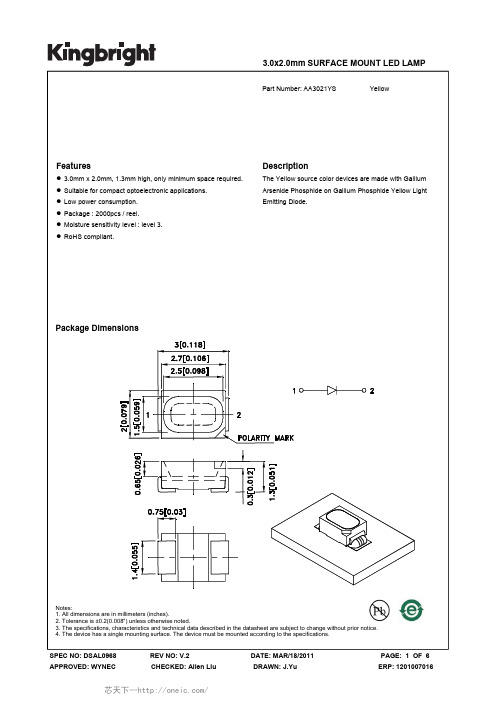
AA3021YS, 规格书,Datasheet 资料
5. As silicone encapsulation is permeable to gases, some corrosive substances such as H2S might corrode silver plating of leadframe. Special care should be taken if an LED with silicone encapsulation is to be used near such substances. SPEC NO: DSAL0968 APPROVED: WYNEC REV NO: V.2 CHECKED: Allen Liu DATE: MAR/18/2011 DRAWN: J.Yu PAGE: 2 OF 6 ERP: 1201007016
REV NO: V.2 CHECKED: Allen Liu
DATE: MAR/18/2011 DRAWN: J.Yu
PAGE: 6 OF 6 ERP: 1201007016
芯天下--/
DATE: MAR/18/2011 DRAWN: J.Yu
PAGE: 4 OF 6 ERP: 1201007016
芯天下--/
AA3021YS
Reflow soldering is recommended and the soldering profile is shown below. Other soldering methods are not recommended as they might cause damage to the product.
Notes: 1. All dimensions are in millimeters (inches). 2. Tolerance is ±0.2(0.008") unless otherwise noted. 3. The specifications, characteristics and technical data described in the datasheet are subject to change without prior notice. 4. The device has a single mounting surface. The device must be mounted according to the specifications.
NJW0302G;NJW0281G;中文规格书,Datasheet资料

NJW0281G (NPN)NJW0302G (PNP)Preferred Devices Complementary NPN-PNP Power Bipolar TransistorsThese complementary devices are lower power versions of the popular NJW3281G and NJW1302G audio output transistors. With superior gain linearity and safe operating area performance, these transistors are ideal for high fidelity audio amplifier output stages and other linear applications.Features•ăExceptional Safe Operating Area•ăNPN/PNP Gain Matching within 10% from 50 mA to 3 A•ăExcellent Gain Linearity•ăHigh BVCEO•ăHigh Frequency•ăThese are Pb-Free DevicesBenefits•ăReliable Performance at Higher Powers•ăSymmetrical Characteristics in Complementary Configurations •ăAccurate Reproduction of Input Signal•ăGreater Dynamic Range•ăHigh Amplifier BandwithApplications•ăHigh-End Consumer Audio Products♦ăHome Amplifiers♦ăHome Receivers•ăProfessional Audio Amplifiers♦ăTheater and Stadium Sound Systems♦ăPublic Address Systems (PAs)MAXIMUM RATINGSRating Symbol Value UnitCollector-Emitter Voltage V CEO250Vdc Collector-Base Voltage V CBO250Vdc Emitter-Base Voltage V EBO 5.0Vdc Collector-Emitter Voltage - 1.5 V V CEX250VdcCollector Current - Continuous-Peak (Note 1)I C1530AdcBase Current - Continuous I B1.5AdcTotal Power Dissipation @ T C = 25°C P D150WattsOperating and Storage Junction Temperature Range T J, T stg-65 to+150°CStresses exceeding Maximum Ratings may damage the device. Maximum Ratings are stress ratings only. Functional operation above the Recommended Operating Conditions is not implied. Extended exposure to stresses above the Recommended Operating Conditions may affect device reliability.1.Pulse Test: Pulse Width = 5.0 ms, Duty Cycle < 10%.15 AMPERES COMPLEMENTARY SILICON POWER TRANSISTORS250 VOLTS, 150 WATTSDevice Package ShippingORDERING INFORMATIONTO-3PCASE 340ABMARKINGDIAGRAMPreferred devices are recommended choices for future use and best overall value.NJW0302G TO-3P(Pb-Free)30 Units/Rail NJW0281G TO-3P(Pb-Free)30 Units/Railxxxx= 0281 or 0302G= Pb-Free PackageA= Assembly LocationY= YearWW= Work WeekNJWxxxGAYWWTHERMAL CHARACTERISTICSCharacteristicSymbol Value Unit Thermal Resistance, Junction-to-CaseR θJC0.83°C/WELECTRICAL CHARACTERISTICS (T C = 25°C unless otherwise noted)CharacteristicSymbolMinMaxUnitOFF CHARACTERISTICSCollector-Emitter Sustaining Voltage (I C = 30 mA, I B = 0)V CEO(sus)250-V Collector Cutoff Current (V CB = 250 V, I E = 0)I CBO -10m A Emitter Cutoff Current (V EB = 5.0 V, I C = 0)I EBO- 5.0m AON CHARACTERISTICS DC Current Gain(I C = 0.5 A, V CE = 5.0 V)(I C = 1.0 A, V CE = 5.0 V)(I C = 3.0 A, V CE = 5.0 V)h FE757575150150150-Collector-Emitter Saturation Voltage (I C = 5.0 A, I B = 0.5 A)V CE(sat)- 1.0V Base-Emitter On Voltage (I C = 5.0 A, V CE = 5.0 V)V BE(on)- 1.2V DYNAMIC CHARACTERISTICSCurrent-Gain - Bandwidth Product(I C = 1.0 A, V CE = 5.0 V, f test = 1.0 MHz)f T 30-MHz Output Capacitance(V CB = 10 V, I E = 0, f test = 1.0 MHz)C ob-400pF160T C , CASE TEMPERATURE (°C)40601001201608014020Figure 1. Power Derating 020406080100140120P D , P O W E R D I S S I P A T I O N (W)0.010.11101001101001000V CE , COLLECTOR-EMITTER VOLTAGE (V)I C , C O L L E C T O R C U R R E N T (A )Figure 2. Safe Operating Area00.20.40.60.811.21.40.010.1110100I C , COLLECTOR CURRENT (A)Figure 3. NJW0281G DC Current GainFigure 4. NJW0302G DC Current Gainh F E , D C C U R R E N T G A I NI C , COLLECTOR CURRENT (A)Figure 5. NJW0281G Base-Emitter Voltage I C , COLLECTOR CURRENT (A)0.010.1110100Figure 6. NJW0302G Base-Emitter VoltageV B E (o n ), B A S E -E M I T T E R V O L T A G E (V )I C , COLLECTOR CURRENT (A)V B E (o n ), B A S E -E M I T T E R V O L T A G E (V )h F E , D C C U R R E N T G A I N0.050.111050-0.10.40.91.41.92.40.050.111050Figure 7. NJW0281G Saturation Voltage 0.010.11100.010.1110100I C , COLLECTOR CURRENT (A)V C E (s a t ), C O L L E C T O R -E M I T T E R S A T U R A T I O N V O L T A G E (V)0.010.11100.010.1110100Figure 8. NJW0302G Saturation VoltageI C , COLLECTOR CURRENT (A)V C E (s a t ), C O L L E C T O R -E M I T T E R S A T U R A T I O N V O L T A G E (V )0102030405060700.010.1110Figure 9. NJW0281G Current Gain BandwidthProduct I C , COLLECTOR CURRENT (A)f T , C U R R E N T G A I N B A N D W I D T H P R O D U C T (M H z )Figure 10. NJW0302G Current Gain BandwidthProductI C , COLLECTOR CURRENT (A)f T , C U R R E N T G A I N B A N D W I D T H P R O D U C T (M H z )01020304050600.010.1110PACKAGE DIMENSIONSTO-3P-3LD CASE 340AB-01ISSUE ADIM A MIN NOM MAX MILLIMETERS 19.7019.9020.10B 15.4015.6015.80C 4.60 4.80 5.00D 0.80 1.00 1.20E 1.45 1.50 1.65G 5.45 BSC H 1.20 1.40 1.60J 0.550.600.75K 19.8020.0020.20L 18.5018.7018.90U 5.00 REF P 3.30 3.50 3.70Q 3.10 3.20 3.50W2.803.00 3.20NOTES:1.DIMENSIONING AND TOLERANCING PER ASME Y14.5M, 1994.2.CONTROLLING DIMENSION: MILLIMETERS3.DIMENSION b APPLIES TO PLATED TERMINAL AND IS MEASURED BETWEEN 0.15 AND 0.30mm FROM THE TERMINAL TIP.4.DIMENSION A AND B DO NOT INCLUDE MOLD FLASH, PROTRUSIONS, OR GATE BURRS.F 1.80 2.00 2.20SEATING PLANEFUON Semiconductor and are registered trademarks of Semiconductor Components Industries, LLC (SCILLC). SCILLC reserves the right to make changes without further notice to any products herein. SCILLC makes no warranty, representation or guarantee regarding the suitability of its products for any particular purpose, nor does SCILLC assume any liability arising out of the application or use of any product or circuit, and specifically disclaims any and all liability, including without limitation special, consequential or incidental damages.“Typical” parameters which may be provided in SCILLC data sheets and/or specifications can and do vary in different applications and actual performance may vary over time. All operating parameters, including “Typicals” must be validated for each customer application by customer's technical experts. SCILLC does not convey any license under its patent rights nor the rights of others. SCILLC products are not designed, intended, or authorized for use as components in systems intended for surgical implant into the body, or other applications intended to support or sustain life, or for any other application in which the failure of the SCILLC product could create a situation where personal injury or death may occur. Should Buyer purchase or use SCILLC products for any such unintended or unauthorized application, Buyer shall indemnify and hold SCILLC and its officers, employees, subsidiaries, affiliates,and distributors harmless against all claims, costs, damages, and expenses, and reasonable attorney fees arising out of, directly or indirectly, any claim of personal injury or death associated with such unintended or unauthorized use, even if such claim alleges that SCILLC was negligent regarding the design or manufacture of the part. SCILLC is an Equal Opportunity/Affirmative Action Employer. This literature is subject to all applicable copyright laws and is not for resale in any manner.PUBLICATION ORDERING INFORMATION分销商库存信息:ONSEMINJW0302G NJW0281G。
HGTG30N60B3;中文规格书,Datasheet资料

Gate to Emitter Plateau Voltage On-State Gate Charge
VGEP QG(ON)
IC = IC110, VCE = 0.5 BVCES IC = IC110, VCE = 0.5 BVCES VGE = 15V VGE = 20V
-
7.2 170 230 36 25 137 58 500 550 680
Features
• 60A, 600V, TC = 25oC • 600V Switching SOA Capability • Typical Fall Time. . . . . . . . . . . . . . . . . 90ns at TJ = 150oC • Short Circuit Rating • Low Conduction Loss
VCE(SAT)
IC = IC110, VGE = 15V
Gate to Emitter Threshold Voltage Gate to Emitter Leakage Current Switching SOA
VGE(TH) IGES SSOA
IC = 250µA, VCE = VGE VGE = ±20V TJ = 150oC, RG = 3Ω, VGE = 15V, L = 100µH
©2004 Fairchild Semiconductor Corporation
HGTG30N60B3 Rev. B3
/
HGTG30N60B3
Absolute Maximum Ratings
TC = 25oC, Unless Otherwise Specified HGTG30N60B3 Collector to Emitter Voltage . . . . . . . . . . . . . . . . . . . . . . . . . . . . . . . . . . . . . . . . . . . . . .BVCES Collector Current Continuous At TC = 25oC . . . . . . . . . . . . . . . . . . . . . . . . . . . . . . . . . . . . . . . . . . . . . . . . . . . . . . . . . IC25 At TC = 110oC . . . . . . . . . . . . . . . . . . . . . . . . . . . . . . . . . . . . . . . . . . . . . . . . . . . . . . . IC110 Collector Current Pulsed (Note 1) . . . . . . . . . . . . . . . . . . . . . . . . . . . . . . . . . . . . . . . . . . . ICM Gate to Emitter Voltage Continuous. . . . . . . . . . . . . . . . . . . . . . . . . . . . . . . . . . . . . . . . . VGES Gate to Emitter Voltage Pulsed . . . . . . . . . . . . . . . . . . . . . . . . . . . . . . . . . . . . . . . . . . . .VGEM Switching Safe Operating Area at TJ = 150oC (Figure 2) . . . . . . . . . . . . . . . . . . . . . . . SSOA Power Dissipation Total at TC = 25oC . . . . . . . . . . . . . . . . . . . . . . . . . . . . . . . . . . . . . . . . . PD Power Dissipation Derating TC > 25oC . . . . . . . . . . . . . . . . . . . . . . . . . . . . . . . . . . . . . . . . . . Reverse Voltage Avalanche Energy . . . . . . . . . . . . . . . . . . . . . . . . . . . . . . . . . . . . . . . . . EARV Operating and Storage Junction Temperature Range . . . . . . . . . . . . . . . . . . . . . . . . TJ, TSTG Maximum Lead Temperature for Soldering . . . . . . . . . . . . . . . . . . . . . . . . . . . . . . . . . . . . . TL Short Circuit Withstand Time (Note 2) at VGE = 12V. . . . . . . . . . . . . . . . . . . . . . . . . . . . . .tSC Short Circuit Withstand Time (Note 2) at VGE = 10V. . . . . . . . . . . . . . . . . . . . . . . . . . . . . .tSC 60 30 220 ±20 ±30 60A at 600V 208 1.67 100 -55 to 150 260 4 10 W W/oC mJSymbolC
3590S-2-502L;3590S-2-102L;3590S-2-103L;3590S-2-203L;3590S-1-502L;中文规格书,Datasheet资料

Specifi cations are subject to change without notice.Customers should verify actual device performance in their specifi c applications.*RoHS Directive 2002/95/EC Jan. 27, 2003 including annex and RoHS Recast 2011/65/EU June 8, 2011.Stop Strength..............................................................................................................................................................................45 N-cm (64 oz.-in.) minimum Mechanical Angle ...........................................................................................................................................................................................3600 ° +10 °, -0 °Torque (Starting & Running) ................................................................................................................................0.35 N-cm (0.5 oz.-in.) maximum (unsealed) 1.1 N-cm (1.5 oz.-in.) maximum (sealed) Mounting ..............................................................................................................................................................................55-80 N-cm (5-7 lb.-in.) (plastic) 90-113 N-cm (8-10 in.-lb.) (metal)Shaft Runout......................................................................................................................................................................................0.13 mm (0.005 in.) teral Runout ...................................................................................................................................................................................0.20 mm (0.008 in.) T.I.R.Shaft End Play ...................................................................................................................................................................................0.25 mm (0.010 in.) T.I.R.Shaft Radial Play ...............................................................................................................................................................................0.13 mm (0.005 in.) T.I.R.Pilot Diameter Runout .......................................................................................................................................................................0.08 mm (0.003 in.) T.I.R.Backlash ............................................................................................................................................................................................................1.0 ° maximum Weight ........................................................................................................................................................................................................Approximately 19 G Terminals ................................................................................................................................................................................................Solder lugs or PC pins Soldering ConditionManual Soldering...........................................................96.5Sn/3.0Ag/0.5Cu solid wire or no-clean rosin cored wire; 370 °C (700 °F) max. for 3 seconds Wave Soldering ...................................................................................96.5Sn/3.0Ag/0.5Cu solder with no-clean fl ux; 260 °C (500 °F) max. for 5 seconds Wash processes .......................................................................................................................................................................................Not recommended Marking .....................................Manufacturer’s name and part number, resistance value and tolerance, linearity tolerance, wiring diagram, and date code.Ganging (Multiple Section Potentiometers) ......................................................................................................................................................1 cup maximum Hardware ............................................................................................................One lockwasher and one mounting nut is shipped with each potentiometer.NOTE: For Anti-rotation pin add 91 after confi guration dash number. Example: -2 becomes -291 to add AR pin.1At room ambient: +25 °C nominal and 50 % relative humidity nominal, except as noted. 2Consult manufacturer for complete specifi cation details for resistances below 1k ohms.BOLDFACE LISTINGS ARE IN STOCK AND READILY AVAILABLETHROUGH DISTRIBUTION. FOR OTHER OPTIONS CONSULT FACTORY.ROHS IDENTIFIER: L = COMPLIANTRecommended Part Numbers(Printed Circuit)(Solder Lug)(Solder Lug)Resistance (Ω)Resolution (%)3590P-2-102L 3590S-2-102L 3590S-1-102L 1,000.0293590P-2-202L 3590S-2-202L 3590S-1-202L 2,000.0233590P-2-502L 3590S-2-502L 3590S-1-502L 5,000.0253590P-2-103L 3590S-2-103L 3590S-1-103L 10,000.0203590P-2-203L 3590S-2-203L 3590S-1-203L 20,000.0193590P-2-503L 3590S-2-503L 3590S-1-503L 50,000.0133590P-2-104L3590S-2-104L3590S-1-104L100,000.009*Ro H S C O MP L I A N T/Panel Thickness Dimensions(For Bushing Mount Only)1.60 +.08/-.03(.063 +.003/-.001)DIA.ANTI-ROTATION PINAnti-rotation pin hole is shown at six o'clockposition for reference only. The actual location isdetermined by the customer's application. Referto the front view of the potentiometer to see thelocation of the optional A/R pin.Panel thickness and hole diameters arerecommended for best fit. However, customersmay adjust the dimensions to suit their specificapplication.Product DimensionsSpecifi cations are subject to change without notice.Customers should verify actual device performance in their specifi c applications.REV. 06/12 MOUNTING SURFACE-2, -4, -6, -8 Confi gurations-1, -3, -5, -7 Confi gurationsRecommended PCB LayoutHOLE DIAMETER5.08(.200)5.08(.200)6.99(.275)SchematicTOLERANCES: EXCEPT WHERE NOTED.508 .127DECIMALS: .XX ±(.02),.XXX ±(.005)FRACTIONS: ±1/64MMDIMENSIONS:(IN.)Shaft & Bushing Confi gurations(Bushing - DxL, Shaft - D):(-1) Plastic Bushing (3/8 ” x 5/16 ”)and Shaft (.2480 + .001, - .002)(-2) Metal Bushing (3/8 ” x 5/16 ”)and Shaft (.2497 + .0000, - .0009)(-3) Sealed, Plastic Bushing (3/8 ” x 5/16 ”)and Shaft (.2480 + .001, - .002)(-4) Sealed, Metal Bushing (3/8 ” x 5/16 ”)and Shaft (.2497 + .0000, - .0009)(-5) Metric, Plastic Bushing (9 mm x 7.94 mm)and Shaft (6 mm + 0, - .076 mm)(-6) Metric, Metal Bushing (9 mm x 7.94 mm)and Shaft (6 mm + 0, - .023 mm)(-7) Metric, Sealed, Plastic Bushing (9 mm x7.94 mm) and Shaft (6 mm + 0, - .076 mm)(-8) Metric, Sealed, Metal Bushing (9 mm x7.94 mm) and Shaft (6 mm + 0, - .023 mm)Terminal Styles“P” Terminal Style“S” Terminal Style/分销商库存信息:BOURNS3590S-2-502L3590S-2-102L3590S-2-103L 3590S-2-203L3590S-1-502L3590S-2-104L 3590S-1-203L3590S-2-501L3590S-2-202L 3590S-1-503L3590S-2-503L3590S-1-104L 3590S-291-102L3590S-291-203L3590S-291-502L 3590S-1-201L3590S-1-501L3590S-2-101L 3590S-2-201L3590P-1-102L3590P-1-103L 3590P-1-201L3590P-1-502L3590S-1-102L 3590S-1-103L3590S-2-252L3590P-291-501L 3590P-2-102L3590P-2-201L3590P-2-203L 3590P-2-502L3590S-1-202L3590S-6-102L 3590S-6-201L3590S-6-202L3590S-6-203L 3590S-6-501L3590P-1-104L3590S-6-502L 3590S-4-102L3590S-4-103L3590S-4-202L 3590S-4-203L3590S-4-502L3590S-8-102L 3590S-8-103L3590S-8-202L3590P-2-104L 3590P-4-103L3590P-4-202L3590S-6-503L 3590S-6-104L3590S-4-104L3590P-4-503L 3590P-4-104L3590S-2-5023590S-1-102 3590S-1-1033590S-1-1043590S-1-203 3590S-1-5023590S-1-5033590S-2-102 3590S-2-1033590S-2-1043590S-2-203 3590S-2-5033590S-1-2023590S-2-202 3590S-2-501。
FGA20N120FTDTU;中文规格书,Datasheet资料
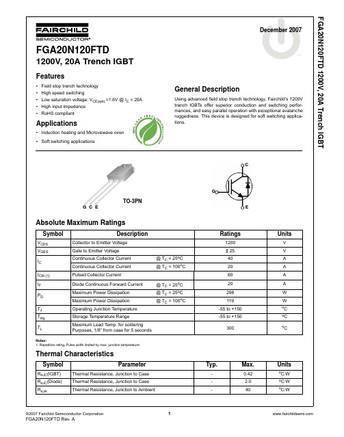
GCE
TO-3PN
Absolute Maximum Ratings
Symbol
VCES VGES IC
ICM (1) IF PD
TJ Tstg TL
Description
Collector to Emitter Voltage Gate to Emitter Voltage Continuous Collector Current Continuous Collector Current Pulsed Collector Current
oC
Typ.
-
Max.
0.42 2.0 40
Units
oC/W oC/W oC/W
FGA20N120FTD 1200V, 20A Trench IGBT
Package Marking and Ordering Information
Device Marking
©2007 Fairchild Semiconductor Corporation
1
FGA20N120FTD Rev. A
G
E
Ratings
1200 ± 25 40 20 60 20 298 119 -55 to +150 -55 to +150 300
Units
V V A A A A W W oC oC
Applications
• Induction heating and Microvewave oven • Soft switching applications
December 2007
tm
General Description
Using advanced field stop trench technology, Fairchild’s 1200V trench IGBTs offer superior conduction and switching performances, and easy parallel operation with exceptional avalanche ruggedness. This device is designed for soft switching applications.
SecuriTEST IP接口数据表说明书
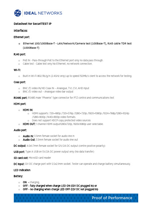
Datasheet for SecuriTEST IPInterfacesEthernet port:o Ethernet 100/1000Base-T - LAN/Network/Camera test (100Base-T), RJ45 cable TDR test (1000Base-T)RJ45 port:o PoE IN - Pass-through PoE to the Ethernet port only no data pass through.o Cable test - Cable test only No Ethernet, no network connection.Wi-Fi:o Built in Wi-Fi 802.11b/g/n (2.4GHz only) up to speed 150Mb/s client to access the network for testing. Coax port:o BNC (f) video IN/HD Coax IN – Analogue, TVI, CVI, AHD inputo BNC (f) video out – Analogue video bar outputRS485 port: RS485 male “Phoenix” type connector for PTZ control and communications testHDMI port:o HDMI IN:o HDMI supports: 720×480p /720×576p /1280×720p /1920×1080p /1024×768p/1280×1024p /1280×900p /1440×900p video formats.o Does not support HDCP copy protected video sourceso HDMI OUT: 1 channel HDMI output1280x720p, 1920x1080p user selectable.Audio port:o Audio IN: 3.5mm female socket for audio line ino Audio Out: 3.5mm female socket for audio line outDC output: 4.0x1.7mm female socket for 12V/2A DC output (centre positive polarity)USB port: Type A USB on 5V/2A DC power output only (No data transfer)SD card slot: MicroSD card readerDC input: 12V DC charge port with 5.5x2.1mm socket. Tester can operate and charge battery simultaneously. LED IndicationBattery:o ON - charging,o OFF - fully charged when charge LED ON (12V DC plugged in) oro OFF - no charging when charge LED OFF (12V DC not plugged in)Flash - battery switch is OFF or no battery fitted (charge LED is ON)o ON - External DC 12V IN is plugged ino OFF - External DC 12V IN is not plugged inTx & Rx:Flash - Tx & Rx data for RS485ON – Standby (both Tx & Rx ON)Test functionsIP Camera Test:o Max video input resolution: 4K (8MP).o Codec support: MJPEG, MPEG4, H.264, H.265 (mainstream)o ONVIF support: relevant part of profile S,Q,Go IP address discovery & assign: auto discover static IP address of direct-connected camera or assign IP address to the camera with dynamic IP address setting ( from internal DHCP server) automatically.o Stream support: RTSP (Real Time Streaming Protocol)o Non ONVIF and proprietary IP camera support: manual IP address, port and model selection for non ONVIF supported cameras brand including ACTi, AIPU, APD, Axis, Aebell, Arecont Vision, BILL, BM,Bestecher, Bosch, CityTech, CYZ, Changying, Colin, Costar, Dahua , DOZENY, DVO, DVSONE, Devele,Etrovision, FOKO, FORSECU, FS, Finetida, GOLBONG, GREAT, Geovision, Grandeye, HI-SHARP, Hikvision, HISIDE, HZWS, HanbangGaoKe, HawKeye, Hitron, Honewell, HuiSun, hongben, ISEC, Infinova, JETVIEW,JOOAN, JOVISION, JUAN, Jbvideo, JieGao, JingShiKang, KEDACOM, KINPUS, KeJun, KumKang, LEFOUND, LILIN, LanDunSiAn, Longse, MaxxOne, NJBESTWAY, Neitway, OSKA, PN3D, Panasonic, Pelco, PengRunDa, Pinshi, QIDUN, Samsung, SANTACHI, SHIKO,SONY, STJIATU, STYCO, Safer, SecurityTronix, Seeyou,SongXin, Sunell, SuperSight, TBTEC, TIANDY, TP-LINK, TVT, TianLong, TruVue, Uniview,VIDIACNET,VIVOTEK, VSTON,VVS-CCTV, VideoNet, Vista, WAPA, WATCHMAN, WEISKY, Woshida,XiangWei, XinLong, YH, YIDUN, YJX, YSJ, YXAF, YueTian, YunShiAn, ZKTeco, ZLD …o PTZ, focus, aperture: Key pad and screen gesture to control of aperture, zoom, focus, pan, tilt.o Digital zoom: Up to 20 times (subject to camera availability)o Rapid video: One key discovery of active network cameras and access to camera setup and programming via ONVIF.Web browser: ChromeAnalogue (CVBS) camera test:o Video input: 1 channel analogue CVBS signal PAL & NTSC auto detectiono Video level meter: Peak video signal level, Sync signal level, Colour, Chroma level measuremento Video output: colour bar, blue or black full screen in NTSC or PAL formats.o Dual window display: CVBS floating on screen of IP camera test results at the same time for analogue and IP converter test monitor and troubleshooting.o PTZ control: Supports RS485 control, Baud 600-115200bps, Compatible with more than 30 protocols such as PELCO-D/P, Samsung, Panasonic, Bosch etc. (for details see HD Coax PTZ part) o PTZ address scan: auto detect camera’s PTZ addresso PTZ data monitoring: Captures and analyses the command data from PTZ controller. Manual transmit of hexadecimal codes in RS485 for PTZ control testing.HD Coax (TVI, CVI, AHD) camera test:o TVI: 8MP (4K) 3840 x 2160 15 fps, 5MP 2592 x 1944P 12.5/20 fps, 4MP 2688 x 1520P 15fps; 2560 x 1440P 15/25/30 fps, 3MP 2048 x 1536P 18/25/30 fps, 2MP (1080P) 1920 x 1080P 25/30 fps, 720P 1280 x 720P25/30/50/60 fps, UTC control/ call OSD menuo CVI: 8MP (4K) 3840 x 2160 12.5/15 fps, 4MP 2560x1440P 25F/30 fps, 1080p 1920 x 1080P 25/30 fps, 720p 1280 x 720P 25/30/50/60fps, UTC control d call OSD menuo AHD: 5MP 2592 x 1944P 12.5/20 fps,4MP 2560x1440P 15/25/30 fps, 3MP 2048x1536P 18/25/30 fps, 1080p 1920x1080P 25/30fps,720P 1280x720P 25/30 fps ,UTC control d call OSD menuo Images: Snapshot/view, video record/play, screenshoto PTZ control:Port type - UTC Coaxitron®:▪PTZ - Address, pan speed, tilt speed, set & recall position▪Menu - arrows control with address•Port type - RS485:▪Protocol: ALEC, AD168(M-B), Bosch OSRD, CBC, DAT-SD, DH-YTC06, Fastrax, HD600, Hikvision, Kalatel ASC, LC-NEW, LG-MULTIX, Lilin-FAST, Lilin-MLP2, Minking A01, MinkingB01, Molynx, Panasonic, Pelco D, Pelco P, Samsung, Samsung SPD, SIEMENS, SONY-EVI,Santachi, TeleEye DM2, Vcltp, Vicon, WV-CS850, YAAN, YAAN-0, YAAN-1▪Baud rate: 150, 300, 600,1200,2400,4800,9600,19200, 38400,115200▪Address, Pand & Tilt speed, Position set & Recallo Zoom: Key pad control manual & digital (5x max)Power output:o PoE: DC48V PoE/PoE+, 24W maxo DC 12V: DC12V/2A power for IP & analogue cameraso DC 5V: DC5V 2A power output via USB to charge portable devicesPoE & Voltage testo PoE IN: voltage, power and pins usedo LAN/Network: voltage, power and pin usedo12V DC IN: voltage, power consumed (operating and charging power consumption)o12V DC OUT: voltage, power consumed by attached deviceo PoE link check: PD (Powered Device) port on cable Tracer/Remote Test’s PoE status of link and pairs used with LED indicators for 12,36 or 45,78 pins.Ethernet cable test:o Twisted-pair test: Reports: – straight, crossed-pair, open, short and cross-over (MDI-MDIX) with Tracer/Remote.o RJ45 TDR test: Length 180m (max), Resolution +/-1m; estimated attenuation (dB/100m or dB/100feet) with good, poor and bad colour status; reflection %; impedance (Ω); delay skew (when connected to1000Mb/s network device only), pin number with pair length. Continuous and single test mode.o Digita l Tone generator: 4 different tone selections for cable tracing.o Cable trace: Trace and locate cables with the included Tracer/Remote. Digital tone technology eliminates electrical noise/hum associated with traditional analogue tracing probes. Eight (8) volume levels,headphone jack for use in noisy environments, non-conductive tip to prevent short circuits and integrated LED flashlight. Requires 2 x 1.5V AAA (LR03) batteries (not included).IP Network test:o Traffic monitoring: real-time upstream/downstream bandwidth histogram, tester IP address and link speed and full/half-duplex condition.o Ping: Local & destination IP address, packet size, number of ping tests and inter-packet delay.o IP Scan: Scan for active devices within selected IP address range (subnet). Scan selected IP address for available TCP/UDP port services.o Port flash: Flash the link LED on of the switch to visually identify the port to which SecuriTEST IP is connected.o DHCP Server: Fully configurable DHCP server to allow dynamically configured devices to operate when a network router is not installed. Start/stop IP address range, lease time, connected client list display.o Trace Route: Display IP address and delay time of up to 30 hops (routers) between device and target URL/IP address.o Available IP: Create list of IP addresses and to scan for availability checking. Tester will scan each address and identify if the address is available or in use by a network device. Use to find available IP addressedwhen before configuring a new device with a static address.o Network IP Scan: Cross-subnet IP scan on any linked network. Lists IP address of devices on multiple subnets compared to IP Scan function which only lists devices on the same subnet as the tester.Media playback/record applications:o Video: RTSP player, Video player, VLCo Audio: Audio recorder, Audio playerImage capture:o Capture still image from connected camera (can be attached to test reports).o Record video stream from connected camera.o Capture current tester screen.Audio:o Audio IN: 1 channel audio signal input from camera to record, listen and play via media player or audio recorder/player; 2.5 mm (1/8”) connector.o Audio OUT: 1 channel audio signal output to monitor audio from cameras with microphone; 2.5 mm (1/8”) connector.o Speaker: Internal two speakers for system indicators and audio playback from cameras or other media files.Test report (ONVIF only): PDF format witho Company/customer project details,o Tester information,•Serial number/hardware version/firmware version/software version•Date/time seto Date/time of test conductedo Camera manufacturer/model/name/software version/Date & timeo Camera network configuration,o Link speed and duplexo IP/gateway/DNS/MAC addresses, subnet masko Dynamic/static configurationo Video stream information,o Video resolutiono Frame rateo Bit rateo Encoding (CODEC) typeo Attach up to six (6) video still snapshot images,o Operator’s noteso Attach company/customer logoQuick Access Shortcut menu: Single button access to eight (8) user-selectable functionsRemote view: View tester screen on other network device using RTSP (Real Time Streaming Protocol).Results & upgradeJOBS: Shortcut to user storage area with folders for Audio/ Logos/ Photos/ Reports/ Screenshots/ Videos. Single button copy all files/directories from internal JOBS folder to external SD card.File management:o File explorer: copy, save, delete, cut, paste, transfer to internal and external SD cardo FTP: results to be accessed and managed via FTP with tester configured as a server or client.o MicroSD card: transfer results to other devices or install software updates.Upgrade: Auto & manual updates from microSD card.HelpVideo introduction: a quick video clip for basic operation introductionUser guide: Context sensitive on-line helpQuick reference guide: a quick reference guide for starting to operate the testerFAQ: a list of commonly asked questions regarding to tester operation.GeneralDisplay:o Screen: 7 inch capacitive touch screen with 1920x1200 resolution (324 ppi).o Screen locking: user password setting for secured tester access.o Screen rotation: rotating screen for ceiling camera adjustment before mounting.o Sleep timer: 1-30 min, disengage.Storage: 10GB internal SD card, 8GB external microSD card included (supports up to 16 GB).Date & Time: Date,Time & time zone selection, 24 hours format, manual and auto sync.Power: Charger: input 110-240VAC, 50/60Hz, 0.6A; output 12VDC, 2A, centre pin positive polarity; US, UK, EU, Australia AC plug adapters.Battery:o Capacity: Field user exchangeable 7.4V Lithium polymer battery, 5000mAh, 37Who Operation time: 10 hour (typical) continuous operation without external PoE/DC12V load; 4.5hours (typical) with 3.5 watt PoE camera load.o Charge time: < 8 hours from empty.Language: English, French, German, Spanish, Italian, Portuguese, ChineseLength units: meter, feetOperating Temperature: -10°C---+50°C / 50° F---122°FOperating Humidity: 30%-90%Dimension 252 mm x 160 mm x 48 mm/ 10.0 in x 6.3 in x 1.9 in (approximate)Weight: 1.0 Kg/2.2 lbs (including battery)Standard complianceCE RED directive:•EN 60950-1:2006+A11:2009+A1:2010+A12:2011+A2:2013•EN 301 489-1 V1.9.2 (2011-09)•EN 301 489-17 V2.2.1 (2012-09)•EN 300 328 V1.9.1 (2015-02)•EN 62479:2010FCC:•FCC Part 15 Subpart BRoHS:•EN62321:2012•EN 14372:2004•EPA 3540:1996Tone Tracer/Remote CE directive:•EN55032:2015•EN61000-3-2:2014•EN61000-3-3:2013•EN55024:2010+A1:2015IDEAL INDUSTRIES NETWORKS DIVISIONUnit 3, Europa Court, Europa Boulevard, Warrington, Cheshire, WA5 7TN, UK. Tel. +44 (0)1925 444 446 | Fax. +44 (0)1925 445501******************** | Specification subject to change without notice. Errors & Omissions Excepted © IDEAL Networks 2018Publication No.: 171870A subsidiary ofIDEAL INDUSTRIES INC.。
ZXTN25020DGTA;中文规格书,Datasheet资料
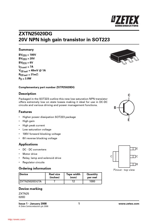
ZXTN25020DG20V NPN high gain transistor in SOT223SummaryBV CEX > 100V BV CEO > 20V BV ECX > 6V I C(cont) = 7AV CE(sat) < 48mV @ 1A R CE(sat) = 31m ΩP D = 3.0WComplementary part number ZXTP25020DGDescriptionPackaged in the SOT223 outline this new low saturation NPN transistor offers extremely low on state losses making it ideal for use in DC-DC circuits and various driving and power management functions.Features•Higher power dissipation SOT223 package •High gain •High peak current •Low saturation voltage •100V forward blocking voltage •6V reverse blocking voltageApplications•DC - DC converters •Motor drive•Relay, lamp and solenoid drive •Regulator circuitsOrdering informationDevice markingZXTN25020DDeviceReel size (inches)Tape width(mm)Quantity per reel ZXTN25020DGTA7121000Absolute maximum ratingsThermal resistanceNOTES:(a)For a device surface mounted on 15mm x 15mm x 0.6mm FR4 PCB with high coverage of single sided 1oz copper, in still air conditions.(b)Mounted on 25mm x 25mm x 0.6mm FR4 PCB with high coverage of single sided 1oz copper, in still air conditions.(c)Mounted on 50mm x 50mm x 0.6mm FR4 PCB with high coverage of single sided 2oz copper, in still air conditions.(d)As (c) above measured at t<5 seconds.(e)Junction to case (collector tab). TypicalParameterSymbol Limit Unit Collector-Base voltageV CBO 100V Collector-Emitter voltage (forward blocking)V CEX 100V Collector-Emitter voltageV CEO 20V Emitter-Collector voltage (reverse blocking)V ECX 6V Emitter-Base voltageV EBO 7V Continuous Collector current (c)I C 7A Base current I B 1A Peak pulse currentI CM 15A Power dissipation at T A =25°C (a)Linear derating factorP D1.29.6W mW/°C Power dissipation at T A =25°C (b)Linear derating factorP D 1.612.8W mW/°C Power dissipation at T A =25°C (c)Linear derating factorP D 3.024W mW/°C Power dissipation at T A =25°C (d)Linear derating factorP D 5.342W mW/°C Power dissipation at T C =25°C (e)Linear derating factorP D 7.358W mW/°C Operating and storage temperature rangeT j , T stg -55 to 150°CParameterSymbol Limit Unit Junction to ambient (a)R ⍜JA 104°C/W Junction to ambient (b)R ⍜JA 78°C/W Junction to ambient (c)R ⍜JA 42°C/W Junction to ambient (d)R ⍜JA 23.5°C/W Junction to case (e)R ⍜JC16°C/WThermal characteristicsElectrical characteristics (at T amb = 25°C unless otherwise stated).Parameter Symbol Min.Typ.Max.Unit Conditions Collector-Base breakdown voltageBV CBO 100125V I C = 100ACollector-Emitter breakdown voltage (forward blocking)BV CEX 100120VI C = 100A, R BE < 1k Ω or-1V < V BE < 0.25V Collector-Emitter breakdown voltage BV CEO 2035V I C = 10mA (*)NOTES:(*)Measured under pulsed conditions. Pulse width ≤ 300µs; duty cycle ≤ 2%.Emitter-Collector breakdown voltage (reverse blocking)BV ECX68.3VI E = 100A, R BC < 1k Ω or0.25V > V BC > -0.25V Emitter-Collector breakdown voltage (reverse blocking)BV ECO 5 6.1VI E = 100A Emitter-Base breakdown voltageBV EBO 78.35V I E = 100ACollector-Base cut-off currentI CBO <1500.5nA A V CB = 100VV CB = 100V, T amb = 100°C Collector-Emitter cut-off currentI CEX100nAV CE = 100V, R BE < 1k Ω or-1V < V BE < 0.25V Emitter cut-off current I EBO <150nA V EB = 5.6VCollector-Emitter saturation voltageV CE(sat)40601001302254875120180290mV mV mV mV mV I C = 1A, I B = 100mA (*)I C = 1A, I B = 20mA (*)I C = 2A, I B = 40mA (*)I C = 2A, I B = 20mA (*)I C = 7A, I B = 700mA (*)Base-Emitter saturation voltageV BE(sat)10901150mV I C = 7A, I B = 700mA (*)Base-Emitter turn-on voltageV BE(on)9501050mVI C = 7A, V CE = 2V (*)Static forward current transfer ratioh FE300250504503608515900I C = 10mA, V CE = 2V (*)I C = 2A, V CE = 2V (*)I C = 7A, V CE = 2V (*)I C = 15A, V CE = 2V (*)Transition frequency f T 215MHz I C = 50mA, V CE = 10V f = 100MHzInput capacitance C ibo 152pFV EB = 0.5V, f = 1MHz (*)Output capacitance C obo 16.525pF V CB = 10V, f = 1MHz (*)Delay time t d 67.7ns I C = 1A, V CC = 10V,I B1 = -I B2 = 10mA Rise time t r 72.2ns Storage time t s 361ns Fall timet f63.9nsZetex sales offices EuropeZetex GmbHKustermann-park Balanstraße 59D-81541 München GermanyTelefon: (49) 89 45 49 49 0Fax: (49) 89 45 49 49 49europe.sales@AmericasZetex Inc700 Veterans Memorial Highway Hauppauge, NY 11788USATelephone: (1) 631 360 2222Fax: (1) 631 360 8222usa.sales@Asia PacificZetex (Asia Ltd)3701-04 Metroplaza Tower 1Hing Fong Road, Kwai Fong Hong KongTelephone: (852) 26100 611Fax: (852) 24250 494asia.sales@Corporate HeadquartersZetex Semiconductors plcZetex Technology Park, Chadderton Oldham, OL9 9LL United KingdomTelephone: (44) 161 622 4444Fax: (44) 161 622 4446hq@© 2008 Published by Zetex Semiconductors plcDefinitionsProduct changeZetex Semiconductors reserves the right to alter, without notice, specifications, design, price or conditions of supply of any product or service. Customers are solely responsible for obtaining the latest relevant information before placing orders.Applications disclaimerThe circuits in this design/application note are offered as design ideas. It is the responsibility of the user to ensure that the circuit is fit for the user’s application and meets with the user’s requirements. No representation or warranty is given and no liability whatsoever is assumed by Zetex with respect to the accuracy or use of such information, or infringement of patents or other intellectual property rights arising from such use or otherwise. Zetex does not assume any legal responsibility or will not be held legally liable (whether in contract,tort (including negligence), breach of statutory duty, restriction or otherwise) for any damages, loss of profit, business, contract,opportunity or consequential loss in the use of these circuit applications, under any circumstances.Life supportZetex products are specifically not authorized for use as critical components in life support devices or systems without the express written approval of the Chief Executive Officer of Zetex Semiconductors plc. As used herein:A. Life support devices or systems are devices or systems which:1.are intended to implant into the body or2.support or sustain life and whose failure to perform when properly used in accordance with instructions for use provided in the labeling can be reasonably expected to result in significant injury to the user.B. A critical component is any component in a life support device or system whose failure to perform can be reasonably expected tocause the failure of the life support device or to affect its safety or effectiveness.ReproductionThe product specifications contained in this publication are issued to provide outline information only which (unless agreed by the company in writing) may not be used, applied or reproduced for any purpose or form part of any order or contract or be regarded as a representation relating to the products or services concerned. Terms and ConditionsAll products are sold subjects to Zetex’ terms and conditions of sale, and this disclaimer (save in the event of a conflict between the two when the terms of the contract shall prevail) according to region, supplied at the time of order acknowledgement.For the latest information on technology, delivery terms and conditions and prices, please contact your nearest Zetex sales office.Quality of productZetex is an ISO 9001 and TS16949 certified semiconductor manufacturer.To ensure quality of service and products we strongly advise the purchase of parts directly from Zetex Semiconductors or one of our regionally authorized distributors. For a complete listing of authorized distributors please visit: /salesnetworkZetex Semiconductors does not warrant or accept any liability whatsoever in respect of any parts purchased through unauthorized sales channels.ESD (Electrostatic discharge)Semiconductor devices are susceptible to damage by ESD. Suitable precautions should be taken when handling and transporting devices.The possible damage to devices depends on the circumstances of the handling and transporting, and the nature of the device. The extent of damage can vary from immediate functional or parametric malfunction to degradation of function or performance in use over time.Devices suspected of being affected should be replaced.Green complianceZetex Semiconductors is committed to environmental excellence in all aspects of its operations which includes meeting or exceeding reg-ulatory requirements with respect to the use of hazardous substances. Numerous successful programs have been implemented to reduce the use of hazardous substances and/or emissions.All Zetex components are compliant with the RoHS directive, and through this it is supporting its customers in their compliance with WEEE and ELV directives.Product status key:“Preview”Future device intended for production at some point. Samples may be available “Active”Product status recommended for new designs “Last time buy (LTB)”Device will be discontinued and last time buy period and delivery is in effect “Not recommended for new designs”Device is still in production to support existing designs and production “Obsolete”Production has been discontinued Datasheet status key:“Draft version”This term denotes a very early datasheet version and contains highly provisional information, whichmay change in any manner without notice.“Provisional version”This term denotes a pre-release datasheet. It provides a clear indication of anticipated performance.However, changes to the test conditions and specifications may occur, at any time and without notice.“Issue”This term denotes an issued datasheet containing finalized specifications. However, changes tospecifications may occur, at any time and without notice.分销商库存信息: DIODESZXTN25020DGTA。
Quectel_EC20_R2.0_硬件设计手册_V1.2
e 3.5.2. 飞行模式 ......................................................................................................................... 29 fid 3.6. 电源设计 ................................................................................................................................ 29
10. 图 31 增加备注 3。
11. 增加射频信号线 Layout 参考指导(5.1.4 章节)。
12. 更新模块耗流数据(表 33)。
13. 增加 GNSS 耗流数据(表 34)。
14. 更新 7.3 章节中模块俯视图。
上海移远通信技术股份ຫໍສະໝຸດ 限公司2 / 83EC20 R2.0 硬件设计手册
目录
3.6.1. 管脚介绍 ......................................................................................................................... 29 3.6.2. 减少电压跌落.................................................................................................................. 30
602-00013;中文规格书,Datasheet资料
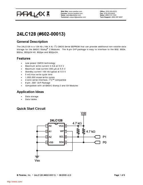
Web Site: Forums: Sales: sales@Technical: support@Office: (916) 624-8333Fax: (916) 624-8003Sales: (888) 512-1024Tech Support: (888) 997-8267 24LC128 (#602-00013)General DescriptionThe 24LC128 is a 128 Kb (16K X 8) I²C CMOS Serial EEPROM that can provide additional non-volatile data storage for the BASIC Stamp® 2Modules. The 8-pin DIP package is easy to interface to the BS2, BS2e, BS2sx, BS2p24/40, BS2pe and BS2px24.Features•Low-power CMOS technology•Maximum write current 3 mA at 5.5 V•Maximum read current 400 µA at 5.5 V•Standby current 100 nA typical at 5.5 V• 5 mS max write cycle time•1,000,000 erase/write cycles•2-wire serial interface, I²C™ compatible•8-pin .300” DIP Package•Compatible with all BASIC Stamp2 and SX ModulesApplication Ideas•Data storage•Data tablesQuick Start CircuitConnecting and TestingConnect the 24LC128 as shown in the Quick Start Circuit, then use the appropriate demo program foryour BASIC Stamp module to verify correct operation. If you are using an SX Microcontroller you will need to write or edit some existing I²C code to access the EEPROM.Resources and DownloadsCheck out the 24LC128 product page for example programs, articles and more:/detail.asp?product_id=602-00013Device InformationPin Definitions and RatingsPin Name Function1 A0 Address Pin 02 A1 Address Pin 13 A2 Address Pin 24 Vss Ground -> 0 V5 SDA Serial Data Input/OutputInput6 SCL SynchronousClockPin7 WP Write-Protect8 Vcc +5 V Power InputSymbol Quantity Minimum Typical Maximum UnitsVoltage 2.5 5.0 6.5 V Vcc SupplyGND Ground 0 V Icc (sb) Standyby Supply Current 100 nACurrent 400 uA Ir ReadIw WriteCurrent 3 mA * Ratings from manufacturer datasheetCommunication ProtocolThe 24LC128 communicates over the I²C bus with various types of transactions, such as Byte Write, Page Write, Random Read and Sequential Read.All communication with the 24LC128 requires a control byte to be sent. This control byte includes a Start Bit, the Control Code (4 bits), the Chip Select (3 bits) and the R/W bit.The address lines (A0, A1, A2) are used to select multiple 24LC128 devices on the same bus. Up to 8 24LC128 devices can be connected to the same bus.Please see the manufacturer datasheet from Microchip for more information on reading/writing data to the 24LC128.Source CodeBASIC Stamp® 2, 2e, 2sx ProgramThis program will allow you to use the 24LC128 with the BASIC Stamp 2, 2e and 2sx.' =========================================================================' File....... 24LC128.bs2' Purpose.... Interface To A 24LC128 16KB EEPROM' Author..... Parallax, Inc.' E-mail..... support@' Updated.... 08-09-2005' {$STAMP BS2}' {$PBASIC 2.5}' -----[ Program Description ]---------------------------------------------' This code will interface the BS2, BS2e and BS2sx to a 24LC128 16KB EEPROM' -----[ I/O Definitions ]-------------------------------------------------SDA PIN 0 ' I2C Serial Data LineSCL PIN 1 ' I2C Serial Clock Line' -----[ Constants ]------------------------------------------------------- Address CON $A0 ' Address Of 24LC128Ack CON 0 ' Acknowledge Bit' -----[ Variables ]-------------------------------------------------------temp VAR Byte ' Variable Used For Worki2cWork VAR Word ' Work Byte For I2C I/Oi2cAck VAR Bit ' Ack Bit From Deviceeeprom_add VAR Word ' EEPROM Address' -----[ Main Routine ]----------------------------------------------------DODEBUG "Enter value to store from 0 to 255: "DEBUGIN DEC3 tempDEBUG CR, "Enter address to store ", DEC temp, " at, 0 to 15999: "DEBUGIN DEC5 eeprom_add' Writing SectionGOSUB I2C_StopGOSUB I2C_StartGOSUB Control_Byte_WriteGOSUB AddrsGOSUB Write_DataGOSUB I2C_StopPAUSE 100' Reading SectionGOSUB I2C_StartPAUSE 10GOSUB Control_Byte_WriteGOSUB AddrsGOSUB I2C_StartGOSUB Control_Byte_ReadSHIFTIN SDA, SCL, LSBFIRST, [i2cwork\8] ' Send Byte To DeviceGOSUB I2C_StopDEBUG CR, "Value stored at location ", DEC eeprom_add," is ", DEC i2cwork.LOWBYTE, CR, CR, CRLOOP' -----[ Subroutines ]----------------------------------------------------- I2C_Stop: ' I2C Stop Bit SequenceLOW SDAINPUT SCLINPUT SDA ' SDA --> High While SCL High RETURNI2C_Start: ' I2C Start Bit SequenceINPUT SDAINPUT SCLLOW SDA ' SDA --> Low While SCL HighRETURNAddrs: ' I2C Address Byte Sequencei2cWork = eeprom_addSHIFTOUT SDA, SCL, MSBFIRST, [i2cWork.HIGHBYTE\8] ' Send Byte To DeviceSHIFTIN SDA, SCL, MSBPRE, [i2cAck\1] ' Get Acknowledge BitSHIFTOUT SDA, SCL, MSBFIRST, [i2cWork.LOWBYTE\8] ' Send Byte To DeviceSHIFTIN SDA, SCL, MSBPRE, [i2cAck\1] ' Get Acknowledge BitRETURNControl_Byte_Write: ' I2C Control Write Byte Sequencei2cWork = Addressi2cWork.BIT0 = 0 ' Sets Unit To WriteSHIFTOUT SDA, SCL, MSBFIRST, [i2cWork\8] ' Send Byte To DeviceSHIFTIN SDA, SCL, MSBPRE, [i2cAck\1] ' Get Acknowledge BitRETURNControl_Byte_Read: ' I2C Control Read Byte Sequencei2cWork = Addressi2cWork.BIT0 = 1 ' Sets Device To ReadSHIFTOUT SDA, SCL, MSBFIRST, [i2cWork\8] ' Send Byte To DeviceSHIFTIN SDA, SCL, MSBPRE, [i2cAck\1] ' Get Acknowledge BitRETURNWrite_Data: ' I2C Write Byte Sequencei2cWork = tempSHIFTOUT SDA, SCL, MSBFIRST, [i2cWork\8] 'Send Byte To DeviceSHIFTIN SDA, SCL, MSBPRE, [i2cAck\1] ' Get Acknowledge BitRETURNBASIC Stamp® 2p, 2pe, 2px ProgramThis program will allow you to use the 24LC128 with the BASIC Stamp 2p, 2pe and 2px.' ========================================================================= ' File....... 24LC128.bsp' Purpose.... Interface To A 24LC128 16KB EEPROM' Author..... Parallax, Inc.' E-mail..... support@' Updated.... 08-09-2005' {$STAMP BS2p}' {$PBASIC 2.5}' -----[ Program Description ]--------------------------------------------- ' This code will interface the BS2p, BS2pe and BS2px to a 24LC128 EEPROM' -----[ I/O Definitions ]------------------------------------------------- SDA PIN 0 ' I2C Serial Data LineSCL PIN 1 ' I2C Serial Clock Line' -----[ Variables ]------------------------------------------------------- value VAR Byte ' Variable Used To Store Value eeprom_add VAR Word ' EEPROM Address' -----[ Main Routine ]---------------------------------------------------- DODEBUG "Enter value to store from 0 to 255: "DEBUGIN DEC3 ValueDEBUG CR, "Enter address to store ", DEC value, " at, 0 to 15999: "DEBUGIN DEC5 eeprom_add' Writing SectionI2COUT SDA, $A0,eeprom_add.HIGHBYTE\eeprom_add.LOWBYTE, [value]PAUSE 20' Reading SectionI2CIN SDA, $A1,eeprom_add.HIGHBYTE\eeprom_add.LOWBYTE, [value]DEBUG CR, "Value stored at location ",DEC eeprom_add," is ", DEC value, CR, CR, CRLOOP分销商库存信息: PARALLAX602-00013。
SDM20U30_1中文资料
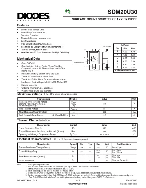
Lead-free GreenSDM20U30SURFACE MOUNT SCHOTTKY BARRIER DIODEFeatures·Low Forward Voltage Drop ·Guard Ring Construction for Transient Protection·Negligible Reverse Recovery Time ·Low Capacitance·Ultra-Small Surface Mount Package·Lead Free By Design/RoHS Compliant (Note 1)·"Green" Device, Note 4 and 5·Qualified to AEC-Q101 Standards for High Reliability·Case: SOD-523·Case Material: Molded Plastic, "Green" Molding Compound, Note 5. UL Flammability Classification Rating 94V-0·Moisture Sensitivity: Level 1 per J-STD-020C ·Terminal Connections: Cathode Band·Terminals: Finish - Matte Tin annealed over Alloy 42leadframe.Solderable per MIL-STD-202, Method 208·Marking Code: LM·Ordering Information: See Last Page ·Weight: 0.002 grams (approximate)Mechanical DataMaximum Ratings@ T A = 25°C unless otherwise specifiedElectrical Characteristics@ T A = 25°C unless otherwise specifiedMARKINGNote:1. No purposefully added lead.2. Part mounted on FR-4 board with recommended pad layout, which can be found on our websiteat /datasheets/ap02001.pdf. T A = 25°C.3. Short duration pulse test used to minimize self-heating effect.4. Diodes Inc.'s "Green" policy can be found on our website at /products/lead_free/index.php.5. Product manufactured with Date Code 0609 (week 9, 2006) and newer are built with Green Molding Compound. Product manufactured prior toDate Code 0609 are built with Non-Green Molding Compound and may contain Halogens or Sb2O3 Fire Retardants.Thermal Characteristics050255075100125P ,P O W E R D I S S I P A T I O N (m W )D T ,AMBIENT TEMPERATURE (C)Fig.1Derating CurveA °100200150.001.01.11101000100200400600800V ,INSTANTANEOUS FORWARD VOLTAGE (mV)Fig.2Typical Forward CharacteristicsF I ,I N S T A N T A N E O U S F O R W A R D C U R R E N T (m A )F5101520253026481012C ,T O T A L C A P A C I T A N C E (p F )T V ,REVERSE VOLTAGE (V)Fig.4Typical Total Capacitancevs.Reverse VoltageR 051015202530I ,I N S T A N T A N E O U S R E V E R S E C U R R E N T (A )R V ,INSTANTANEOUSREVERSE VOLTAGE (V)Fig.3Typical Reverse CharacteristicsR 100n10m1mOrdering Information(Note 4 & 6)Note:4.Product manufactured with Date Code 0609 (week 9, 2006) and newer are built with Green Molding Compound. Product manufactured prior to Date Code 0609 are built with Non-Green Molding Compound and may contain Halogens or Sb2O3 Fire Retardants.6. For Packaging Details, go to our website at /datasheets/ap02007.pdf.IMPORTANT NOTICEDiodes Incorporated and its subsidiaries reserve the right to make modifications,enhancements,improvements,corrections or other changes without further notice to any product herein.Diodes Incorporated does not assume any liability arising out of the application or use of any product described herein;neither does it convey any license under its patent rights,nor the rights of others.The user of products in such applications shall assume all risks of such use and will agree to hold Diodes Incorporated and all the companies whose products are represented on our website,harmless against all damages.LIFE SUPPORTDiodes Incorporated products are not authorized for use as critical components in life support devices or systems without the expressed written approval of the President of Diodes Incorporated.。
VUE30-20NO1中文资料
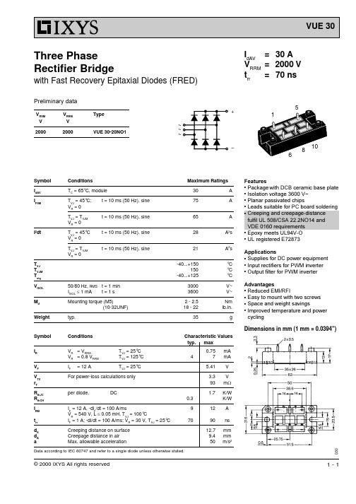
Three Phase Rectifier Bridge
with Fast Recovery Epitaxial Diodes (FRED)
Preliminary data
VRSM V 2000 VRRM V 2000 Type ~ ~ ~ – +
IdAV = 30 A VRRM = 2000 V trr = 70 ns
Maximum Ratings 30 75 65 28 21 -40...+150 150 -40...+125 A A A A2s As °C °C °C V~ V~ Nm lb.in. g
2
I2dt
TVJ = 45°C VR = 0 TVJ = TVJM VR = 0
Features Package with DCB ceramic base plate Isolation voltage 3600 V~ Planar passivated chips Leads suitable for PC board soldering Creeping and creepage-distance fulfil UL 508/CSA 22.2NO14 and VDE 0160 requirements Epoxy meets UL94V-O UL registered E72873
q q q q
Dimensions in mm (1 mm = 0.0394")
Symbol IR VF VT0 rT RthJC RthCH IRM trr dS dA a Conditions VR = VRRM VR = 0.8 VRRM IF = 12 A TVJ = 25°C TVJ = 125°C TVJ = 25°C Characteristic Values typ. max 4 0.75 7 5.41 3.3 93 1.7 0.3 IF = 12 A, -diF/dt = 100 A/ms VR = 540 V, L £ 0.05 mH, TVJ = 100°C IF = 1 A; -di/dt = 100 A/ms; VR = 30 V, TVJ = 25°C Creeping distance on surface Creepage distance in air Max. allowable acceleration 9 70 12 90 12.7 9.4 50 mA mA V V mW K/W K/W A ns mm mm m/s2
IXDA20N120AS;IXDA20N120AS-TUBE;中文规格书,Datasheet资料
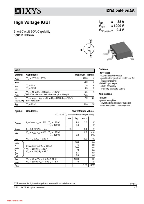
20110118aIXYS reserves the right to change limits, test conditions and dimensions.I C25 = 38 AV CES= 1200 V V CE(sat) typ = 2.4 VHigh Voltage IGBTShort Circuit SOA Capability Square RBSOAFeatures• NPT IGBT- low saturation voltage- positive temperature coefficient for easy paralleling • TO-263 package - SMD assembly- industry standard outline Applications• drives• power supplies- switched mode power supplies- uninterruptible power suppliesSymbol Conditions Maximum RatingsV CES T VJ = 25°C to 150°C 1200V V GES ±20V I C25I C90T C = 25°C T C = 90°C3825A A I CM V CEK V GE = 15 V; R G = 82 W ; T VJ = 125°CRBSOA, clamped inductive load; L = 100 µH 35V CES At SC(SCSOA)V CE = V CES ; V GE = ±15 V; R G = 82 W ; T VJ = 125°C non-repetitive 10µs P tot T C = 25°C 200W SymbolConditionsCharacteristic Values(T VJ = 25°C, unless otherwise specified)min.typ.max.V CE(sat)I C = 20 A; V GE = 15 V; T VJ = 25°C T VJ = 125°C 2.42.63.0V V V GE(th)I C = 0.6 mA; V GE = V CE4.56.5V I CES V CE = V CES ; V GE = 0 V; T VJ = 25°C T VJ = 125°C 0.80.8mA mA I GES V CE = 0 V ; V GE = ± 20 V200nA t d(on)t rt d(off)t f E on E off Inductive load; T VJ = 125°C V CE = 600 V; I C = 20 A V GE = ±15 V; R G = 82 W10075500703.12.4ns ns ns ns mJ mJ C ies Q Gon V CE = 25 V; V GE = 0 V; f = 1 MHz V CE = 600 V; V GE = 15 V; I C = 18 A100070pF nC R thJC0.63K/WhTAB20110118aIXYS reserves the right to change limits, test conditions and dimensions.Symbol ConditionsMaximum Ratings T VJ T stg -55...+150-55...+125°C °CSymbol Conditions Characteristic Values min.typ.max.Weight2gmin max min max A4.06 4.830.1600.190A1b 0.510.990.0200.039b2 1.14 1.400.0450.055c 0.400.740.0160.029c2 1.14 1.400.0450.029D8.389.400.3300.370D18.008.890.3150.350E 9.6510.410.3800.410E1 6.228.200.2450.323e H 14.6115.880.5750.625L 1.78 2.790.0700.110L1 1.02 1.680.0400.066L2 1.02 1.520.0400.060Wtyp.0.020.040typ.0.00080.0016All dimensions conform with and/or are within JEDEC standard.limeter Inches 2,54BSC typ. 0.10typ. 0.0040,100BSC20110118aIXYS reserves the right to change limits, test conditions and dimensions.0.00.51.01.52.02.53.03.50510152025303540010203040506070809051015200.00.51.01.52.02.53.03.54.00510152025303540567891011125101520253035V CE [V]I C [A]Q G [nC]I C [A]V CE [V]I C [A]V GE [V]V GE [V]Fig. 1 Typ. output characteristics Fig. 2 Typ. output characteristicsFig. 3 Typ. transfer characteristicsFig. 4 Typ. turn on gate charge20110118aIXYS reserves the right to change limits, test conditions and dimensions.01020304012345670204060801001201400102030401234501002003004005000.000010.00010.0010.010.110.00010.0010.010.11105010015020025030035012340400800120016000501001502002503003504812080160240200400600800100012001400I C [A]I C [A]E on [mJ]t [ns]t[ns]R G [Ω]V CE [V]t [s]I CM [A]Z thJC [K/W]E off [mJ]E off [mJ]t [ns]t[ns]E on [mJ]R G [Ω]Fig. 5 Typ. turn on energy and switching times versus collector currentFig. 7 Typ. turn on energy and switching times versus gate resistor Fig.8 Typ. turn off energy and switchingtimes versus gate resistorFig. 9 Reverse biased safe operating area RBSOAFig. 10 Typ. transient thermal impedanceFig. 6 Typ. turn off energy and switchingtimes versus collector current分销商库存信息:IXYSIXDA20N120AS IXDA20N120AS-TUBE。
LDA201S, 规格书,Datasheet 资料
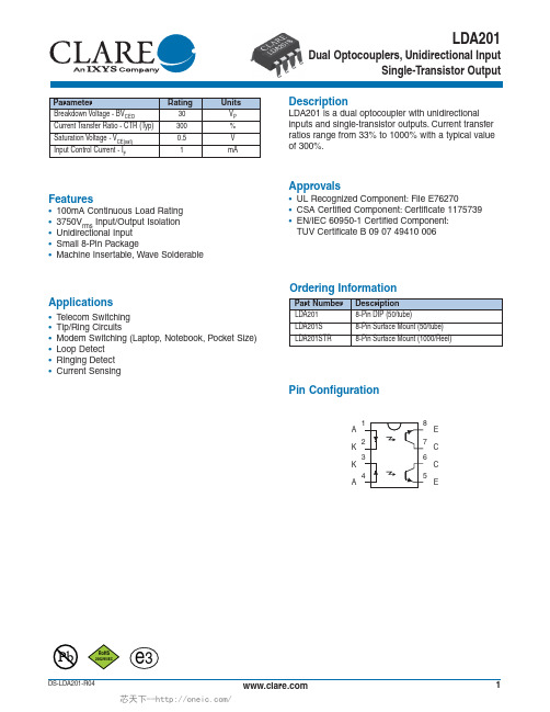
Dual Optocouplers, Unidirectional InputSingle-Transistor OutputLDA201e 3PbApplicationsFeaturesDescriptionOrdering InformationPin Configuration• T elecom Switching • Tip/Ring Circuits• Modem Switching (Laptop, Notebook, Pocket Size)• Loop Detect • Ringing Detect • Current Sensing• 100mA Continuous Load Rating • 3750V rms Input/Output Isolation • Unidirectional Input • Small 8-Pin Package• Machine Insertable, Wave SolderableLDA201 is a dual optocoupler with unidirectional inputs and single-transistor outputs. Current transfer ratios range from 33% to 1000% with a typical value of 300%.ApprovalsE EC C A K KA • UL Recognized Component: File E76270• CSA Certified Component: Certificate 1175739• EN/IEC 60950-1 Certified Component: TUV Certificate B 09 07 49410 006Absolute Maximum Ratings are stress ratings. Stresses in excess of these ratings can cause permanent damage to the device. Functional operation of the device at conditions beyond those indicated in the operational sections of this data sheet is not implied.Absolute Maximum Ratings @ 25ºC2 Derate linearly 2mW / ºCElectrical Characteristics @ 25ºCSwitching Characteristics @ 25ºCSwitching Time Test CircuitVVCEI FPulse Width=5ms Duty Cycle=1%PERFORMANCE DATA**The Performance data shown in the graphs above is typical of device performance. For guaranteed parameters not indicated in the written specifi cations, please contact our application department.LED Forward Voltage (V)1.01.11.2 1.3 1.4 1.5 1.6L E D F o r w a r d C u r r e n t (m A )010********LED Voltage vs. Current (Linear)(T=25ºC)LED Forward Voltage (V)1.01.11.2 1.3 1.4 1.5 1.6L E D F o r w a r d C u r r e n t (m A )0.1110100LED Voltage vs. Current (Log)(T =25ºC)Temperature (ºC)-40-2020406080100L E D F o r w a r d V o l t a g e (V )1.01.11.21.31.41.51.6LED Forward Voltage vs. TemperatureLED Forward Current (mA)0102030405060C u r r e n t T r a n s f e r R a t i o (%)100200300400500600700Typical CTR vs. LED Forward Current(V =5V, T =25ºC)Collector Voltage (V)123456C o l l e c t o r C u r r e n t (m A )20406080100Typical Collector Current vs.Collector Voltage(T =25ºC)Temperature (ºC)I C E C u r r e n t (m A )I CE Current vs. Temperature(V=5V)20406080100Temperature (ºC)-40-20020406080100S a t u r a t i o n V o l t a g e (V )0.080.100.120.140.160.180.20Saturation Voltage vs. Temperature(I =2mA, I=1mA)Temperature (ºC)-40-20020406080100B l o c k i n g V o l t a g e (V P )87888990919293949596Blocking Voltage vs. TemperatureTemperature (ºC)-40-20020406080100L e a k a g e C u r r e n t (n A )0100200300400500Collector Leakage Currentvs. TemperatureLoad Resistance (:)1001k10k 100k1M T u r n -O n T i m e (P s )02468101214Turn-On Time vs. Load Resistance(V =5V, T =25ºC)Load Resistance (k :)0100200300400500600T u r n -O f f T i m e (m s )246810Turn-Off Time vs. Load Resistance(V =5V, T =25ºC)Manufacturing InformationMoisture SensitivityAll plastic encapsulated semiconductor packages are susceptible to moisture ingression. Clare classified allof its plastic encapsulated devices for moisture sensitivity according to the latest version of the joint industry standard, IPC/JEDEC J-STD-020, in force at the time of product evaluation. We test all of our products to the maximum conditions set forth in the standard, and guarantee proper operation of our devices when handled according to the limitations and information in that standard as well as to any limitations set forth in the information or standards referenced below.Failure to adhere to the warnings or limitations as established by the listed specifications could result in reduced product performance, reduction of operable life, and/or reduction of overall reliability.This product carries a Moisture Sensitivity Level (MSL) rating as shown below, and should be handled according to the requirements of the latest version of the joint industry standard IPC/JEDEC J-STD-033.ESD SensitivityThis product is ESD Sensitive, and should be handled according to the industry standard JESD-625. Reflow ProfileThis product has a maximum body temperature and time rating as shown below. All other guidelines of J-STD-020 must be observed.Board WashClare recommends the use of no-clean flux formulations. However, board washing to remove flux residue is acceptable. Since Clare employs the use of silicone coating as an optical waveguide in many of its optically isolated products, the use of a short drying bake may be necessary if a wash is used after solder reflow processes. Chlorine-based or Fluorine-based solvents or fluxes should not be used. Cleaning methods that employ ultrasonic energy should not be used.e3PbMECHANICAL DIMENSIONS LDA201LDA201SDimensionsmm(inches)PCB Hole Pattern9.652 ± 0.3817.620 ± 0.254(0.01)Dimensionsmm(inches)PCB Land Pattern1.65Clare, Inc. makes no representations or warranties with respect to the accuracy or completeness of the contents of this publication and reserves the right to make changes to specifications and product descriptions at any time without notice. Neither circuit patent licenses nor indemnity are expressed or implied. Except as set forth in Clare’s Standard T erms and Conditions of Sale, Clare, Inc. assumes no liability whatsoever, and disclaims any express or implied warranty, relating to its products including, but not limited to, the implied warranty of merchantability, fitness for a particular purpose, or infringement of any intellectual property right.The products described in this document are not designed, intended, authorized or warranted for use as components in systems intended for surgical implant into the body, or in other applications intended to support or sustain life, or where malfunction of Clare’s product may result in direct physical harm, injury, or death to a person or severe property or environmental damage. Clare, Inc. reserves the right to discontinue or make changes to its products at any time without notice.Specification: DS-LDA201-R04©Copyright 2011, Clare, Inc.All rights reserved. Printed in USA.For additional information please visit our website at: 6MECHANICAL DIMENSIONS (Cont.)LDA201S Tape & ReelDimensionsmm (inches)K 1 =4.20(0.165)0 K(0.193)。
30-001-A-01;30-001-A-03;30-001-A-04;30-001-A-05;30-001-A-06;中文规格书,Datasheet资料
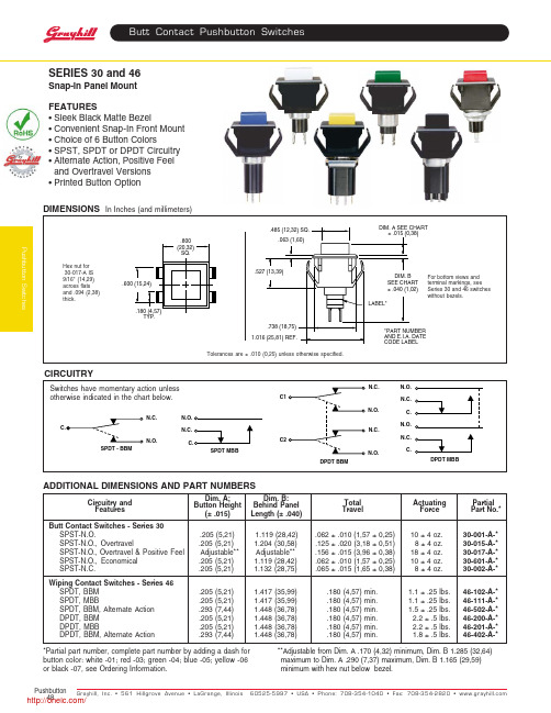
N.C. N.O. N.C. N.O.
N.O. N.C.
C. N.O. N.C.
C.
DPDT MBB
ADDITIONAL DIMENSIONS AND PART NUMBERS
Circuitry and Features
Dim. A:
Dim. B:
Button Height Behind Panel
.800 (20,32)
SQ.
.600 (15,24)
.485 (12,32) SQ. .063 (1,60)
.527 (13,39)
.180 (4,57) TYP.
.738 (18,75) 1.016 (25,81) REF.
Tolerances are ± .010 (0,25) unless otherwise specified.
30-001-A-04 30-001-A-07 30-015-A-04 30-0015-A-07 30-002-A-04 30-002-A-07 30-017-A-03 30-017-A-06 30-05-01-502-04 30-05-01-502-07 30-01-01-500-04 30-01-01-500-07 30-05-04-502-04 30-05-04-502-07 30-01-04-500-04 30-01-04-500-07
(± .015)
Length (± .040)
Butt Contact Switches - Series 30 SPST-N.O. SPST-N.O., Overtravel SPST-N.O., Overtravel & Positive Feel SPST-N.O., Economical SPST-N.C.
Oracle AutoVue VueLink 20.0 用户指南说明书
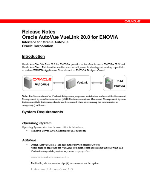
Release NotesOracle AutoVue VueLink 20.0 for ENOVIA Interface for Oracle AutoVueOracle CorporationIntroductionOracle AutoVue VueLink 20.0 for ENOVIA provides an interface between ENOVIA PLM and Oracle AutoVue. This interface enables users to add powerful viewing and markup capabilities to various ENOVIA Application Centrals such as ENOVIA Designer Central.Note: For Oracle AutoVue VueLink Integration programs, installation and use of the Document Management System Customization (DMS Customization) and Document Management System Extension (DMS Extension) should not be counted when determining the total number of computer(s) to license.System RequirementsOperating SystemOperating Systems that have been certified in this release:•Windows Server 2008 R2 Enterprise (32-bit mode)AutoVue•Oracle AutoVue 20.0.0 (and any higher service pack for 20.0.0)Note: Prior to deploying the VueLink, you must locate and disable the following 19.3VueLink-compatibility option in jvueserver.properties:dms.vuelink.version=19.3To disable, add the number sign (#) to comment-out the option:# dms.vuelink.version=19.3ENOVIA Server installation•ENOVIA Live Collaboration Server V6R2011•MQL component of ENOVIA Studio Modeling Platform V6R2011 (required by InstallShield Setup Program for installing schema)•Business Modeler component of ENOVIA Studio Modeling Platform V6R2011 (required to grant business privileges to Administrator user)•ENOVIA Live Collaboration Business Process Services V6R2011•ENOVIA Designer Central V6R2011 (Optional)•ENOVIA File Collaboration Server V6R2011 (Optional)•Matrix Navigator of ENOVIA Studio Modeling Platform V6R2011—required to configure the SolidWorks Integration—(Optional)Application Server / Servlet EngineServers that have been certified in this release:•Tomcat6.0.20New Features•Support for ENOVIA PLM V6R2011•Support for enhanced security provided by AutoVue 20Features Added in Earlier Releases•Support for viewing markups from Related Markup page•Support for viewing renditions from Derived Output page•Support for search of files stored in ENOVIA repository•Support for batch print of files stored in ENOVIA through browse & search•Support for cross probe of ECAD files stored in ENOVIA through browse & search •Support for digital mockup of ECAD and 3D files stored in ENOVIA through browse and search•Support for ENOVIA installed in a cluster environment•Support for file browse•Support for ENOVIA data model defined by Integration Exchange Framework IEF•Support for new Common Document Model (CDM)•Support for ENOVIA File Collaboration Server•Support for AutoCAD XRefs stored by MXi AutoCAD•Support for CATIA 4 Models stored by MXi CATIA with their transformation matrices •Support for Bookmarks where 2D Drawings contain links to 3D assemblies/parts•Support for Pro/ENGINEER Assemblies/Parts/Family Tables stored by Mxi Pro/ENGINEER integration•Support for ENOVIA Java Programs (JPO) defined in print codes forheader/footer/watermark•Support for normal/master/consolidated markup types in ENOVIA Live Collaboration Business Process Services environment•Support for ENOVIA Live Collaboration Server setup in RIP (Platform Server In Process) mode•Enhanced installer with support for:•eMatrix WAR Utility for packaging•eMatrix WAR/EAR files for J2EE deployment•Automatic configuration of Offline Streaming file caching utility•Support for AutoVue Real-Time Collaboration•Support for viewing documents stored in ENOVIA repository including 3D MCAD assemblies•Support for external reference files (XREFs)•Support for markup/redlining with markups being stored inside ENOVIA repository •Support for normal/master/consolidated markup types with AutoVue schema •Support for opening markups which belong to previous revisions of base document •Support for automatic markup promotion•Support for international (Korean, Japanese, etc.) characters in markup filenames using UTF-8•Support for document attributes to be printed in footer/header/watermark•Support for print notification messages from AutoVue Server•Support for file conversion to TIFF stored in ENOVIA repository as viewables •Support for file compare among revisions of a document stored in ENOVIA repository •Support for online caching of streaming files into ENOVIA repository as viewables •Support for offline caching of streaming files into ENOVIA repository using streaming file caching utility as viewables•Setup Program for automatic installation of VueLink•Support for HTTPS/SSL environment•Support for ENOVIA Live Collaboration Business Process Services schema for 3D CAD Models and assemblies•VueLink configuration is saved in a global business object inside ENOVIA and also inside VueLink properties file•Support for Single Sign On (SSO) with internal/external authentication•Support for ENOVIA Live Collaboration Business Process Services with ENOVIA Designer Central along with other CentralsIncluded in the Media Packdms_extensionThis folder contains a list of files that have been developed to extend DMS functionality. Thesefiles are called by VueLink servlet to run various queries inside DMS.vuelink_documentationThis folder contains Oracle AutoVue VueLink for ENOVIA documentation which contains:User’s ManualDescribes various features supported by Oracle AutoVue VueLink for ENOVIA, such asfile viewing, and opening and saving markups.System Administrator guideDescribes step by step procedure for installing and configuring Oracle AutoVue VueLinkfor ENOVIA.Manual Installation GuideDescribes step by step procedure for manually installing Oracle AutoVueVueLink for ENOVIA.vuelink_servletThis folder contains the following files:•vuelink.jar : VueLink java classes•vueservlet.jar : VueServlet java classes•commons-httpclient.jar : Apache Common HTTP package•commons-logging.jar : Apache Common logging packageTemplatepage•csiApplet.html:•csiLaunch.properties : VueLink properties file•xrefschema.xml : XRefs schema XML file•vuelink.properites : VueLink properties fileetcThis folder contains the following files:releasenotes.pdfThis document.•filelist.txtList of files and folder structure.•version.txtBuild and build date information of this release.•3rdPartyThis folder contains licenses of all third party components that have been bundled withVueLink e.g. The Apache Software Foundation (/).•Acknowledgements.pdf:This file lists 3rd party software components used by VueLink.streaming_file_utilityThis folder contains the streaming file caching utility for ENOVIA. Please refer to readme.html in this folder for instructions.vuelink_setupThis folder contains the installer for VueLink.Known IssuesWhen using the ENOVIA DEC Browse option from the File Open dialog of AutoVue, you will not be able to select a file if there is a folder that shares the same name and is located at the same hierarchy level as the file. To workaround this issue, you can revert to the 19.3 File Open dialog by setting the EnableUniversalFileChooser option to 0 in the allusers.ini file located in the Oracle AutoVue bin folder.For example, you may experience this issue when selecting a CAD file that was checked in from SolidWorks integration with Derived Outputs or ThumbnailViewable as there will be folder with the same name as the file.Copyright © 1998, 2010, Oracle and/or its affiliates. All rights reserved.Oracle is a registered trademark of Oracle Corporation and/or its affiliates. Other names may be trademarks of their respective owners.This software and related documentation are provided under a license agreement containing restrictions on use and disclosure and are protected by intellectual property laws. Except as expressly permitted in your license agreement or allowed by law, you may not use, copy, reproduce, translate, broadcast, modify, license, transmit, distribute, exhibit, perform, publish or display any part, in any form, or by any means. Reverse engineering, disassembly, or decompilation of this software, unless required by law for interoperability, is prohibited.The information contained herein is subject to change without notice and is not warranted to be error-free. If you find any errors, please report them to us in writing.If this software or related documentation is delivered to the U.S. Government or anyone licensing it on behalf of the U.S. Government, the following notice is applicable:U.S. GOVERNMENT RIGHTSPrograms, software, databases, and related documentation and technical data delivered to U.S. Government customers are "commercial computer software" or "commercial technical data" pursuant to the applicable Federal Acquisition Regulation and agency-specific supplemental regulations. As such, the use, duplication, disclosure, modification, and adaptation shall be subject to the restrictions and license terms set forth in the applicable Government contract, and, to the extent applicable by the terms of the Government contract, the additional rights set forth in FAR 52.227-19, Commercial Computer Software License (December 2007). Oracle USA, Inc., 500 Oracle Parkway, Redwood City, CA 94065.This software is developed for general use in a variety of information management applications. It is not developed or intended for use in any inherently dangerous applications, including applications which may create a risk of personal injury. If you use this software in dangerous applications, then you shall be responsible to take all appropriate fail-safe, backup, redundancy and other measures to ensure the safe use of this software. Oracle Corporation and its affiliates disclaim any liability for any damages caused by use of this software in dangerous applications.This software and documentation may provide access to or information on content, products and services from third parties. Oracle Corporation and its affiliates are not responsible for and expressly disclaim all warranties of any kind with respect to third party content, products and services. Oracle Corporation and its affiliates will not be responsible for any loss, costs, or damages incurred due to your access to or use of third party content, products or services.。
AutoVue for Agile PLM 20.1.1 版本 PDF 说明书

AutoVue for Agile PLMReadmeVersion 20.1.1Part Number: E25496-01November 2011ReadmeOracle CopyrightCopyright © 1995, 2011, Oracle and/or its affiliates. All rights reserved.This software and related documentation are provided under a license agreement containing restrictions on use and disclosure and are protected by intellectual property laws. Except as expressly permitted in your license agreement or allowed by law, you may not use, copy, reproduce, translate, broadcast, modify, license, transmit, distribute, exhibit, perform, publish or display any part, in any form, or by any means. Reverse engineering, disassembly, or decompilation of this software, unless required by law for interoperability, is prohibited.The information contained herein is subject to change without notice and is not warranted to be error-free. If you find any errors, please report them to us in writing.If this software or related documentation is delivered to the U.S. Government or anyone licensing it on behalf of the U.S. Government, the following notice is applicable:U.S. GOVERNMENT RIGHTSPrograms, software, databases, and related documentation and technical data delivered to U.S. Government customers are "commercial computer software" or "commercial technical data" pursuant to the applicable Federal Acquisition Regulation and agency-specific supplemental regulations. As such, the use, duplication, disclosure, modification, and adaptation shall be subject to the restrictions and license terms set forth in the applicable Government contract, and, to the extent applicable by the terms of the Government contract, the additional rights set forth in FAR 52.227-19, Commercial Computer Software License (December 2007). Oracle USA, Inc., 500 Oracle Parkway, Redwood City, CA 94065.This software is developed for general use in a variety of information management applications. It is not developed or intended for use in any inherently dangerous applications, including applications which may create a risk of personal injury. If you use this software in dangerous applications, then you shall be responsible to take all appropriate fail-safe, backup, redundancy and other measures to ensure the safe use of this software. Oracle Corporation and its affiliates disclaim any liability for any damages caused by use of this software in dangerous applications.Oracle and Java are registered trademarks of Oracle Corporation and/or its affiliates. Other names may be trademarks of their respective owners.This software and documentation may provide access to or information on content, products and services from third parties. Oracle Corporation and its affiliates are not responsible for and expressly disclaim all warranties of any kind with respect to third party content, products and services. Oracle Corporation and its affiliates will not be responsible for any loss, costs, or damages incurred due to your access to or use of third party content, products or services. The RMW product includes software developed by the Visigoth Software Society.C ONTENTSOracle Copyright (ii)Known Issues (v)Agile AutoVue 20.1.1 Resolved Issues (v)PrefaceOracle's Agile PLM documentation set includes Adobe® Acrobat PDF files. The Oracle Technology Network (OTN) Web site /technetwork/documentation/agile-085940.html contains the latest versions of the Agile PLM PDF files. You can view or download these manuals from the Web site, or you can ask your Agile administrator if there is an Agile PLM Documentation folder available on your network from which you can access the Agile PLM documentation (PDF) files.Note To read the PDF files, you must use the free Adobe Acrobat Reader version 9.0 or later.This program can be downloaded from the Adobe Web site .The Oracle Technology Network (OTN) Web site/technetwork/documentation/agile-085940.html can be accessed through Help > Manuals in both Agile Web Client and Agile Java Client. If you need additional assistance or information, please contact My Oracle Support (https://) for assistance.Note Before calling Oracle Support about a problem with an Agile PLM manual, please have the full part number, which is located on the title page.TTY Access to Oracle Support ServicesOracle provides dedicated Text Telephone (TTY) access to Oracle Support Services within the United States of America 24 hours a day, 7 days a week. For TTY support, call 800.446.2398. Outside the United States, call +1.407.458.2479.ReadmeAny last-minute information about Agile PLM can be found in the Readme file on the Oracle Technology Network (OTN) Web site /technetwork/documentation/agile-085940.html.Agile Training AidsGo to the Oracle University Web page/education/chooser/selectcountry_new.html for more information on Agile Training offerings.Accessibility of Code Examples in DocumentationScreen readers may not always correctly read the code examples in this document. The conventions for writing code require that closing braces should appear on an otherwise empty line; however, some screen readers may not always read a line of text that consists solely of a bracket or brace.This documentation may contain links to Web sites of other companies or organizations that Oracle does not own or control. Oracle neither evaluates nor makes any representations regarding the accessibility of these Web sites.Known Issues BUG #9569916 - AUTOVUE MOBILE LINUX VERSION IS NOT WORKING AS EXPECTED. Issue: On OEL versions other than OEL5.4, the AutoVue Mobile Pack is not supported via the installer.Workaround:1. Shutdown AutoVue.2. Go to the AutoVue installation's bin folder.3. Rename or copy 'libprivilege.so.20.0.0.7330' to 'libprivilege.so.20.0.0.7330.bak'.4. Copy the 'libprivilege.so.20.0.0.7330' file from the CD - \Linux\AutoVueMobilePackPatch to thebin folder.5. Restart AutoVue and check mobile support.Agile AutoVue 20.1.1 Resolved Issues Internal Defect Number: 10219652Service Request Number: 3-2183405101, 3-2216982501,3-4520787971Issue: Right-mouse button (RMB) menu is not available when starting AutoVue for Agile with Web Client View button or Redline buttonRoot Cause:Necessary AutoVue for Agile GUI file missing.Resolution:Provide correct GUI file that is installed with AutoVue 20.1.1 for Agile.Verification:1. Log in to Web Client or to Java Client.2. Create a Part, add attachments.3. Create a change on Part.4. Navigate to Affected Item tab.5. From Redline attachments tab, select a file to view.6. Verify RMB options in View mode.7. From Redline attachments tab select the file to redline.8. Verify RMB options in Redline mode.Right-mouse button options are available in View and Redline modes. Internal Defect Number: 12709745Service Request Number: 3-3936414771Issue: User has no PrintFile privilege but is able to print file in Viewer Root Cause:Necessary AutoVue for Agile GUI file missing.Resolution:Provide correct GUI file that is installed with AutoVue 20.1.1 for Agile.Verification:1. Log in to Java Client.2. Create a user without PrintFile privilege.3. Log in to Web Client or to Java Client.4. Create a Part, add attachments.5. Verify Print option in viewer.Print option is not available in Viewer.。
GE公司NanoVue微型光度计中文说明书
用户手册
1 / 90
目录 1 安装 1.1 1.2 1.3 2. 简介 2.1 2.2 2.3 2.4 2.5 2.6 2.7 2.8 2.9 3 您的 NanoVue 测试仪..................................…………………........................ ..……........…....……........................6 文件系统 数据输出.................................... ...... ......………………….................... ...………...........………..............................7 样品处理………..................................................................... …………………… ...........…...........………...............7 光路长度和吸光度标化……….........................................................................………........... ...................................8 自动读取………..................................................................................... ...........……………………… .......................8 质量保证………..................................................................................... ................………………………..................9 键板和显示屏………..................................................................................... ..........………………… ........................9 软件风格………...........................................................................................................……………………………...11 打开包装和安放...................................................................... ........…… .............................……….........……..........4 安全性.................................................................. ..............................................…….......…............…….…..............4 合格性声明............................................................................ .........……… ...........……................……......................4
- 1、下载文档前请自行甄别文档内容的完整性,平台不提供额外的编辑、内容补充、找答案等附加服务。
- 2、"仅部分预览"的文档,不可在线预览部分如存在完整性等问题,可反馈申请退款(可完整预览的文档不适用该条件!)。
- 3、如文档侵犯您的权益,请联系客服反馈,我们会尽快为您处理(人工客服工作时间:9:00-18:30)。
© 2000 IXYS All rights reserved
1 - 1
Three Phase Rectifier Bridge
with Fast Recovery Epitaxial Diodes (FRED)
Symbol Conditions Maximum Ratings I dAV T C = 65°C, module 30A I FSM
T VJ = 45°C;
t = 10 ms (50 Hz), sine 75A V R = 0T VJ = T VJM t = 10 ms (50 Hz), sine 65A V R = 0
I 2dt
T VJ = 45°C t = 10 ms (50 Hz), sine 28A 2s V R = 0T VJ = T VJM t = 10 ms (50 Hz), sine
21
A 2s V R = 0
T VJ -40...+150
°C T VJM 150°C T stg -40...+125
°C V ISOL 50/60 Hz, RMS t = 1 min 3000V~I ISOL £ 1 mA t = 1 s 3600V~M d Mounting torque (M5)
2 - 2.5Nm (10-32UNF)18 - 22
lb.in.
Weight
typ.
35
g
Data according to IEC 60747 and refer to a single diode unless otherwise stated.
V RSM V RRM Type
V V 2000
2000
VUE 30-20NO1
Features
q Package with DCB ceramic base plate q Isolation voltage 3600 V~q Planar passivated chips
q Leads suitable for PC board soldering q Creeping and creepage-distance fulfil UL 508/CSA 22.2NO14 and VDE 0160 requirements q Epoxy meets UL94V-O q
UL registered E72873
Applications
q Supplies for DC power equipment q Input rectifiers for PWM inverter q
Output filter for PWM inverter
Advantages
q Reduced EMI/RFI
q Easy to mount with two screws q Space and weight savings
q
Improved temperature and power cycling
Dimensions in mm (1 mm = 0.0394")
I dAV = 30 A V RRM = 2000 V t rr =
70 ns
Symbol Conditions Characteristic Values typ.max I R V R = V RRM
T VJ = 25°C 0.75
mA V R = 0.8 V RRM T VJ = 125°C 4
7mA V F I F
= 12 A
T VJ = 25°C
5.41V V T0For power-loss calculations only 3.3V r T 93m W R thJC per diode,
DC
1.7
K/W R thCH 0.3
K/W I RM I F = 12 A, -di F /dt = 100 A/ms
912A V R = 540 V, L £ 0.05 mH, T VJ = 100°C
t rr I F = 1 A; -di/dt = 100 A/ms; V R = 30 V, T VJ = 25°C 70
90ns d S Creeping distance on surface 12.7mm d A Creepage distance in air 9.4mm a
Max. allowable acceleration
50
m/s 2
030
~~~
–+
Preliminary data
/
分销商库存信息: IXYS
VUE30-20NO1。
