HIP4082IP中文数据手册
pic24各个模块数据手册(中文)8章interrupt
8.2.1 软陷阱
算术错误陷阱 (优先级 11)和堆栈错误陷阱 (优先级 12)归类为 “软”陷阱源。软陷阱可以如
同不可屏蔽中断源一样对待,后者的优先级由其在 IVT 中的位置分配。软陷阱的处理方式与中断
类似,在异常处理之前需要 2 个周期进行采样和响应。因此,在响应软陷阱之前可以执行另外的
0x000104 0x000106 0x000108 0x00010A 0x00010C 0x00010E 0x000110 0x000112
保留 振荡器故障 地址错误 堆栈错误 算术错误 保留 保留 保留
陷阱源
© 2007 Microchip Technology Inc.
超前信息
DS39707A_CN 第 8-3 页
优先级。如果与某个中断源相关的 IPCn 位全都清零,则实际上禁止了该中断源。
注: 在器件复位时,器件会初始化 IPCn 寄存器,为所有用户中断源都分配优先级 4。
因为可能会有多个中断请求源分配了同一个特定优先级,所以提供了一种以给定用户分配级别的 方法来解决优先级冲突。每个中断源都具有一个自然顺序优先级,该优先级基于它在 IVT 中的单 元位置。编号较低的中断向量具有较高的自然优先级,而编号较高的向量具有较低的自然优先 级。例如,中断向量 0 具有最高的自然优先级,而中断向量 117 具有最低的自然优先级。所有等 待处理的中断源的总体优先级首先根据用户在 IPCn 寄存器中分配的优先级确定,然后再根据 IVT 中的自然顺序优先级确定。
注:
IVT 和 AIVT 中的所有未实现或未用的向量单元应设定为默认中断处理程序的地址, 该地址中含有一条 RESET 指令。
DS39707A_CN 第 8-2 页
超前信息
微小电子ZL40202精密LVPECL4 1输出缓冲器数据手册说明书

1FeaturesInputs/Outputs •Accepts differential or single-ended input •LVPECL, LVDS, CML, HCSL, LVCMOS •Four precision LVPECL outputs •Operating frequency up to 750 MHzPower •Option for 2.5 V or 3.3 V power supply •Core current consumption of 62 mA•On-chip Low Drop Out (LDO) Regulator for superior power supply noise rejectionPerformance •Ultra low additive jitter of 39 fs RMSApplications•General purpose clock distribution •Low jitter clock trees •Logic translation•Clock and data signal restoration•Wired communications: OTN, SONET/SDH, GE, 10 GE, FC and 10G FC•PCI Express generation 1/2/3 clock distribution •Wireless communications•High performance microprocessor clock distributionApril 2014Figure 1 - Functional Block DiagramZL40202Precision 1:4 LVPECL Fanout BufferData SheetOrdering InformationZL40202LDG1 16 Pin QFN TraysZL40202LDF116 Pin QFN Tape and ReelMatte TinPackage size: 3 x 3 mm-40o C to +85o CTable of ContentsFeatures . . . . . . . . . . . . . . . . . . . . . . . . . . . . . . . . . . . . . . . . . . . . . . . . . . . . . . . . . . . . . . . . . . . . . . . . . . . . . . . . . 1 Applications . . . . . . . . . . . . . . . . . . . . . . . . . . . . . . . . . . . . . . . . . . . . . . . . . . . . . . . . . . . . . . . . . . . . . . . . . . . . . 1 Change Summary . . . . . . . . . . . . . . . . . . . . . . . . . . . . . . . . . . . . . . . . . . . . . . . . . . . . . . . . . . . . . . . . . . . . . . . . . 41.0 Package Description . . . . . . . . . . . . . . . . . . . . . . . . . . . . . . . . . . . . . . . . . . . . . . . . . . . . . . . . . . . . . . . . . . . .52.0 Pin Description. . . . . . . . . . . . . . . . . . . . . . . . . . . . . . . . . . . . . . . . . . . . . . . . . . . . . . . . . . . . . . . . . . . . . . . . .53.0 Functional Description . . . . . . . . . . . . . . . . . . . . . . . . . . . . . . . . . . . . . . . . . . . . . . . . . . . . . . . . . . . . . . . . . .63.1 Clock Inputs. . . . . . . . . . . . . . . . . . . . . . . . . . . . . . . . . . . . . . . . . . . . . . . . . . . . . . . . . . . . . . . . . . . . . . . . .63.2 Clock Outputs . . . . . . . . . . . . . . . . . . . . . . . . . . . . . . . . . . . . . . . . . . . . . . . . . . . . . . . . . . . . . . . . . . . . . .113.3 Device Additive Jitter. . . . . . . . . . . . . . . . . . . . . . . . . . . . . . . . . . . . . . . . . . . . . . . . . . . . . . . . . . . . . . . . .153.4 Power Supply . . . . . . . . . . . . . . . . . . . . . . . . . . . . . . . . . . . . . . . . . . . . . . . . . . . . . . . . . . . . . . . . . . . . . .163.4.1 Sensitivity to power supply noise. . . . . . . . . . . . . . . . . . . . . . . . . . . . . . . . . . . . . . . . . . . . . . . . . . .163.4.2 Power supply filtering. . . . . . . . . . . . . . . . . . . . . . . . . . . . . . . . . . . . . . . . . . . . . . . . . . . . . . . . . . . .163.4.3 PCB layout considerations. . . . . . . . . . . . . . . . . . . . . . . . . . . . . . . . . . . . . . . . . . . . . . . . . . . . . . . .164.0 AC and DC Electrical Characteristics . . . . . . . . . . . . . . . . . . . . . . . . . . . . . . . . . . . . . . . . . . . . . . . . . . . . .175.0 Performance Characterization . . . . . . . . . . . . . . . . . . . . . . . . . . . . . . . . . . . . . . . . . . . . . . . . . . . . . . . . . . .206.0 Typical Behavior . . . . . . . . . . . . . . . . . . . . . . . . . . . . . . . . . . . . . . . . . . . . . . . . . . . . . . . . . . . . . . . . . . . . . .217.0 Package Thermal Characteristics . . . . . . . . . . . . . . . . . . . . . . . . . . . . . . . . . . . . . . . . . . . . . . . . . . . . . . . .238.0 Mechanical Drawing . . . . . . . . . . . . . . . . . . . . . . . . . . . . . . . . . . . . . . . . . . . . . . . . . . . . . . . . . . . . . . . . . . .24List of FiguresFigure 1 - Functional Block Diagram . . . . . . . . . . . . . . . . . . . . . . . . . . . . . . . . . . . . . . . . . . . . . . . . . . . . . . . . . . . . 1 Figure 2 - Pin Connections . . . . . . . . . . . . . . . . . . . . . . . . . . . . . . . . . . . . . . . . . . . . . . . . . . . . . . . . . . . . . . . . . . . 5 Figure 3 - LVPECL Input DC Coupled Thevenin Equivalent . . . . . . . . . . . . . . . . . . . . . . . . . . . . . . . . . . . . . . . . . . 6 Figure 4 - LVPECL Input DC Coupled Parallel Termination. . . . . . . . . . . . . . . . . . . . . . . . . . . . . . . . . . . . . . . . . . . 7 Figure 5 - LVPECL Input AC Coupled Termination . . . . . . . . . . . . . . . . . . . . . . . . . . . . . . . . . . . . . . . . . . . . . . . . . 7 Figure 6 - LVDS Input DC Coupled . . . . . . . . . . . . . . . . . . . . . . . . . . . . . . . . . . . . . . . . . . . . . . . . . . . . . . . . . . . . . 8 Figure 7 - LVDS Input AC Coupled . . . . . . . . . . . . . . . . . . . . . . . . . . . . . . . . . . . . . . . . . . . . . . . . . . . . . . . . . . . . . 8 Figure 8 - CML Input AC Coupled . . . . . . . . . . . . . . . . . . . . . . . . . . . . . . . . . . . . . . . . . . . . . . . . . . . . . . . . . . . . . . 9 Figure 9 - HCSL Input AC Coupled . . . . . . . . . . . . . . . . . . . . . . . . . . . . . . . . . . . . . . . . . . . . . . . . . . . . . . . . . . . . . 9 Figure 10 - CMOS Input DC Coupled Referenced to VDD/2. . . . . . . . . . . . . . . . . . . . . . . . . . . . . . . . . . . . . . . . . 10 Figure 11 - CMOS Input DC Coupled Referenced to Ground . . . . . . . . . . . . . . . . . . . . . . . . . . . . . . . . . . . . . . . . 10 Figure 12 - Simplified Output Driver. . . . . . . . . . . . . . . . . . . . . . . . . . . . . . . . . . . . . . . . . . . . . . . . . . . . . . . . . . . . 11 Figure 13 - LVPECL Basic Output Termination . . . . . . . . . . . . . . . . . . . . . . . . . . . . . . . . . . . . . . . . . . . . . . . . . . . 11 Figure 14 - LVPECL Parallel Output Termination. . . . . . . . . . . . . . . . . . . . . . . . . . . . . . . . . . . . . . . . . . . . . . . . . . 12 Figure 15 - LVPECL Parallel Thevenin-Equivalent Output Termination. . . . . . . . . . . . . . . . . . . . . . . . . . . . . . . . . 12 Figure 16 - LVPECL AC Output Termination for Externally Terminated LVPECL Inputs . . . . . . . . . . . . . . . . . . . . 13 Figure 17 - LVPECL AC Output Termination for Internally Terminated LVPECL Inputs. . . . . . . . . . . . . . . . . . . . . 13 Figure 18 - LVPECL AC Output Termination for CML Inputs. . . . . . . . . . . . . . . . . . . . . . . . . . . . . . . . . . . . . . . . . 14 Figure 19 - Additive Jitter. . . . . . . . . . . . . . . . . . . . . . . . . . . . . . . . . . . . . . . . . . . . . . . . . . . . . . . . . . . . . . . . . . . . 15 Figure 20 - Decoupling Connections for Power Pins. . . . . . . . . . . . . . . . . . . . . . . . . . . . . . . . . . . . . . . . . . . . . . . 16 Figure 21 - Differential Voltage Parameter. . . . . . . . . . . . . . . . . . . . . . . . . . . . . . . . . . . . . . . . . . . . . . . . . . . . . . . 18 Figure 22 - Input To Output Timing . . . . . . . . . . . . . . . . . . . . . . . . . . . . . . . . . . . . . . . . . . . . . . . . . . . . . . . . . . . . 19Change SummaryPage ItemChange1Applications Added PCI Express clock distribution.5Pin Description Added exposed pad to Pin Description.6, 7Figure 3 and Figure 413Figure 16Corrected LVPECL interface circuit.18Figure 21Clarification of V ID and V OD .Below are the changes from the February 2013 to the April 2014 issue:Page Item Change7Figure 4Changed text to indicate the circuit is not recommended for VDD_driver=2.5V.7Figure 5Changed pull-up and pull-down resistors from 2kOhm to 100 Ohm.Below are the changes from the November 2012 issue to the February 2013 issue:Removed 22 Ohm series resistors from Figure 3 and 4.These resistors are not required; however there is no impact to performance if the resistors are included.The device is packaged in a 16 pin QFN1416642out3_nvddout3_pN Cc l k _pvddgndout0_no u t 2_no u t 2_po u t 1_n81210o u t 1_pc l k _nN Cout0_pgndFigure 2 - Pin Connections2.0 Pin DescriptionPin # Name Description1, 4clk_p, clk_n,Differential Input (Analog Input). Differential (or singled ended) input signals. For all input signal configuration see “Clock Inputs” on page 615,14, 12, 11, 10, 9, 7, 6out0_p, out0_n out1_p, out1_n out2_p, out2_n out3_p, out3_nDifferential Output (Analog Output). Differential outputs.8, 13vdd Positive Supply Voltage. 2.5 V DC or 3.3 V DC nominal.5, 16gnd Ground. 0 V.2, 3NCNo Connection. Leave unconnected.Exposed PadDevice GND .The ZL40202 is an LVPECL clock fanout buffer with four identical output clock drivers capable of operating at frequencies up to 750MHz.Inputs to the ZL40202 are externally terminated to allow use of precision termination components and to allow full flexibility of input termination. The ZL40202 can accept DC coupled LVPECL or LVDS and AC coupled LVPECL, LVDS, CML or HCSL input signals; single ended input signals can also be accepted. A pin compatible device with internal termination is also available.The ZL40202 is designed to fan out low-jitter reference clocks for wired or optical communications applications while adding minimal jitter to the clock signal. An internal linear power supply regulator and bulk capacitors minimize additive jitter due to power supply noise. The device operates from 2.5V+/-5% or 3.3V+/-5% supply. Its operation is guaranteed over the industrial temperature range -40°C to +85°C.The device block diagram is shown in Figure 1; its operation is described in the following sections.3.1 Clock InputsThe ZL40202 is adaptable to support different types of differential and singled-ended input signals depending on the passive components used in the input termination. The application diagrams in the following figures allow the ZL40202 to accept LVPECL, LVDS, CML, HCSL and single-ended inputs.Figure 3 - LVPECL Input DC Coupled Thevenin EquivalentFigure 4 - LVPECL Input DC Coupled Parallel TerminationFigure 5 - LVPECL Input AC Coupled TerminationFigure 6 - LVDS Input DC CoupledFigure 7 - LVDS Input AC CoupledFigure 8 - CML Input AC CoupledFigure 9 - HCSL Input AC CoupledFigure 11 - CMOS Input DC Coupled Referenced to GroundVDD_driver R1 (kΩ)R2 (kΩ)R3 (kΩ)RA (kΩ) C (pF) 1.5 1.25 3.075open10101.81 3.8open10102.50.33 4.2open10103.30.75open4.21010Table 1 - Component Values for Single Ended Input Reference to Ground* For frequencies below 100 MHz, increase C to avoid signal integrity issues.3.2 Clock OutputsLVPECL has a very low output impedance and a differential signal swing between 1V and 1.6 V. A simplified diagram for the output stage is shown in Figure 12.The LVPECL to LVDS output termination is not shown since there is a separate device that has the same input and LVDS outputs.out_pout_nFigure 12 - Simplified Output DriverThe methods to terminate the ZL40202 LVPECL drivers are shown in the following figures.Figure 15 - LVPECL Parallel Thevenin-Equivalent Output TerminationF igure 16 - LVPECL AC Output Termination for Externally Terminated LVPECL InputsFigure 17 - LVPECL AC Output Termination for Internally Terminated LVPECL InputsFigure 18 - LVPECL AC Output Termination for CML Inputs3.3 Device Additive JitterThe ZL40202 clock fan out buffer is not intended to filter clock jitter. The jitter performance of this type of device is characterized by its additive jitter. Additive jitter is the jitter the device would add to a hypothetical jitter-free clock as it passes through the device. The additive jitter of the ZL40202 is random and as such it is not correlated to the jitter of the input clock signal.The square of the resultant random RMS jitter at the output of the ZL40202 is equal to the sum of the squares of the various random RMS jitter sources including: input clock jitter; additive jitter of the buffer; and additive jitter due to power supply noise. There may be additional deterministic jitter sources that are not shown in Figure 19.Figure 19 - Additive Jitter3.4 Power SupplyThis device operates with either a 2.5V supply or 3.3V supply.3.4.1 Sensitivity to power supply noisePower supply noise from sources such as switching power supplies and high-power digital components such as FPGAs can induce additive jitter on clock buffer outputs. The ZL40202 is equipped with a low drop out (LDO) power regulator and on-chip bulk capacitors to minimize additive jitter due to power supply noise. The LDO regulator on the ZL40202 allows this device to have superior performance even in the presence of external noise sources. The on-chip regulation, recommended power supply filtering, and good PCB layout all work together to minimize the additive jitter from power supply noise.The performance of these clock buffers in the presence of power supply noise is detailed in ZLAN-403, “Power Supply Rejection in Clock Buffers” which is available from Applications Engineering.3.4.2 Power supply filteringFor optimal jitter performance, the device should be isolated from the power planes connected to its power supply pins as shown in Figure 20.•10 µF capacitors should be size 0603 or size 0805 X5R or X7R ceramic, 6.3 V minimum rating•0.1 µF capacitors should be size 0402 X5R ceramic, 6.3 V minimum rating•Capacitors should be placed next to the connected device power pins• a 0.3 ohm resistor is recommended for the filter shown in Figure 20Figure 20 - Decoupling Connections for Power Pins3.4.3 PCB layout considerationsThe power nets in Figure 20 can be implemented either as a plane island or routed power topology without changing the overall jitter performance of the device.Absolute Maximum Ratings*Parameter Sym.Min.Max.Units 1Supply voltage V DD_R-0.5 4.6V 2Voltage on any digital pin V PIN-0.5V DD V 3LVPECL output current I out30mA 4Soldering temperature T260 °C 5Storage temperature T ST-55125 °C 6Junction temperature T j125 °C 7Voltage on input pin V input V DD V 8Input capacitance each pin C p500fF 4.0 AC and DC Electrical Characteristics* Exceeding these values may cause permanent damage. Functional operation under these conditions is not implied.* Voltages are with respect to ground (GND) unless otherwise statedRecommended Operating Conditions*Characteristics Sym.Min.Typ.Max.Units1Supply voltage 2.5 V mode V DD25 2.375 2.5 2.625V2Supply voltage 3.3 V mode V DD33 3.135 3.3 3.465V3Operating temperature T A-402585°C* Voltages are with respect to ground (GND) unless otherwise statedDC Electrical Characteristics - Current ConsumptionCharacteristics Sym.Min.Typ.Max.Units Notes 1Supply current LVPECL drivers -unloadedI dd_unload62mA Unloaded2Supply current LVPECL drivers - loaded (all outputs are active)I dd_load140mA Including powerto R L = 50DC Electrical Characteristics - Inputs and Outputs - for 3.3 V SupplyCharacteristics Sym.Min.Typ.Max.Units Notes 1Differential input common modevoltageV CM 1.1 2.0V2Differential input voltage difference V ID0.251V3LVPECL output high voltage V OH V DD-1.40V* This parameter is measured from 125 MHz to 750 MHz* This parameter is measured from 125 MHz to 750 MHzFigure 21 - Differential Voltage Parameter* Supply voltage and operating temperature are as per Recommended Operating Conditions4LVPECL output low voltage V OL V DD -1.62V 5LVPECL output differential voltage*V OD0.50.9VDC Electrical Characteristics - Inputs and Outputs - for 2.5 V SupplyCharacteristicsSym.Min.Typ.Max.Units Notes1Differential input common mode voltageV CM 1.1 1.6V 2Differential input voltage difference V ID 0.251V 3LVPECL output high voltage V OH V DD -1.40V 4LVPECL output low voltage V OL V DD -1.62V 5LVPECL output differential voltage*V OD0.40.9VAC Electrical Characteristics* - Inputs and Outputs (see Figure 22) - for 2.5 and 3.3 V supplies.CharacteristicsSym.Min.Typ.Max.Units Notes1Maximum Operating Frequency 1/t p 750MHz 2Input to output clock propagation delay t pd 012ns 3Output to output skew t out2out 50100ps 4Part to part output skewt part2part 80300ps 5Output clock Duty Cycle degradation t PWH / t PWL-2%0%2%Duty Cycle 6LVPECL Output slew rater sl0.75 1.2V/nsDC Electrical Characteristics - Inputs and Outputs - for 3.3 V SupplyCharacteristicsSym.Min.Typ.Max.Units NotesInputt Pt PWL t pdt PWHOutputFigure 22 - Input To Output TimingAdditive Jitter at 2.5 V*Output Frequency (MHz)Jitter MeasurementFilterTypical RMS (fs)Notes112512 kHz - 20 MHz 1122212.512 kHz - 20 MHz 803311.0412 kHz - 20 MHz 70442512 kHz - 20 MHz 65550012 kHz - 20 MHz 566622.0812 kHz - 20 MHz 46775012 kHz - 20 MHz44Additive Jitter at 3.3 V*Output Frequency (MHz)Jitter MeasurementFilterTypical RMS (fs)Notes112512 kHz - 20 MHz 1122212.512 kHz - 20 MHz 823311.0412 kHz - 20 MHz 72442512 kHz - 20 MHz 63550012 kHz - 20 MHz 526622.0812 kHz - 20 MHz 43775012 kHz - 20 MHz395.0 Performance Characterization*The values in this table were taken with an approximate input slew rate of 0.8 V/ns*The values in this table were taken with an approximate input slew rate of 0.8 V/nsAdditive Jitter from a Power Supply Tone*Carrier frequencyParameterTypicalUnitsNotes125MHz 25 mV at 100 kHz 159fs RMS 750MHz25 mV at 100 kHz82fs RMS* The values in this table are the additive periodic jitter caused by an interfering tone typically caused by a switching power supply. For this test, measurements were taken over the full temperature and voltage range for V DD = 3.3 V. The magnitude of the interfering tone is measured at the DUT.6.0 Typical BehaviorTypical Phase Noise at 622.08 MHzTypical Waveform at 155.52 MHzInput Slew Rate versus Additive Jitter Propagation Delay versus TemperatureNote:This is for a single device. For more details see thecharacterization section.V ODversus FrequencyPower Supply Tone Magnitude versus PSRR (at 100 kHz) at 125 MHz Power Supply Tone Magnitude versus Additive Jitter (at 100 kHz) at 125 MHzPower Supply Tone Frequency (at 25 mV) versus PSRR at 125 MHz Power Supply Tone Frequency (at 25 mV) versus Additive Jitter at 125 MHz7.0 Package Thermal Characteristics*Proper thermal management must be practiced to ensure that T jmax is not exceeded.Thermal DataParameterSymbolTest ConditionValue UnitJunction to Ambient Thermal ResistanceΘJAStill Air 1 m/s 2 m/s 67.961.658.1oC/WJunction to Case Thermal Resistance ΘJC Still Air 44.1o C/W Junction to Board Thermal Resistance ΘJB Still Air23.2oC/WMaximum Junction Temperature*T jmax 125o C Maximum Ambient TemperatureT A85oC© 2014 Microsemi Corporation. All rights reserved. Microsemi and the Microsemi logo are trademarks of Microsemi Corporation. All other trademarks and service marks are the property of their respective owners.Microsemi Corporation (NASDAQ: MSCC) offers a comprehensive portfolio of semiconductor and system solutions for communications, defense and security, aerospace and industrial markets. Products include high-performance and radiation-hardened analog mixed-signal integrated circuits, FPGAs, SoCs and ASICs; power management products; timing and synchronization devices and precise time solutions, setting the world’s standard for time; voice processing devices; RF solutions; discrete components; security technologies and scalable anti-tamper products; Power-over-Ethernet ICs and midspans; as well as custom design capabilities and services. Microsemi is headquartered in Aliso Viejo, Calif. and has approximately 3,400 employees globally. Learn more at .Microsemi Corporate Headquarters One One Enterprise, Aliso Viejo CA 92656 USA Within the USA: +1 (800) 713-4113Outside the USA: +1 (949) 380-6100Sales: +1 (949) 380-6136Fax: +1 (949) 215-4996E-mail: ***************************Information relating to products and services furnished herein by Microsemi Corporation or its subsidiaries (collectively “Microsemi”) is believed to be reliable. However, Microsemi assumes no liability for errors that may appear in this publication, or for liability otherwise arising from the application or use of any such information, product or service or for any infringement of patents or other intellectual property rights owned by third parties which may result from such application or use. Neither the supply of such information or purchase of product or service conveys any license, either express or implied, under patents or other intellectual property rights owned by Microsemi or licensed from third parties by Microsemi, whatsoever. Purchasers of products are also hereby notified that the use of product in certain ways or in combination with Microsemi, or non-Microsemi furnished goods or services may infringe patents or other intellectual property rights owned by Microsemi.This publication is issued to provide information only and (unless agreed by Microsemi in writing) may not be used, applied or reproduced for any purpose nor form part of any order or contract nor to be regarded as a representation relating to the products or services concerned. The products, their specifications, services and other information appearing in this publication are subject to change by Microsemi without notice. No warranty or guarantee express or implied is made regarding the capability, performance or suitability of any product or service. Information concerning possible methods of use is provided as a guide only and does not constitute any guarantee that such methods of use will be satisfactory in a specific piece of equipment. It is the user’s responsibility to fully determine the performance and suitability of any equipment using such information and to ensure that any publication or data used is up to date and has not been superseded. Manufacturing does not necessarily include testing of all functions or parameters. These products are not suitable for use in any medical and other products whose failure to perform may result in significant injury or death to the user. All products and materials are sold and services provided subject to Microsemi’s conditions of sale which are available on request.For more information about all Microsemi productsvisit our website at TECHNICAL DOCUMENTATION – NOT FOR RESALE。
美森电路保护设备数据手册说明书

:3 Number of Poles/Left of handle 1, 2, 3, 4, etc. (N = Neutral)Number ofPoles/Rightof handleBlank =< 200A non-fused,_____RevisionBlank =SSpecialConfigurationS = side-operatedN = Non-fusedswitched NeutralUL 98 FusibleDisconnect SwitchesD I S CO N NE C T SW I TC H E SGearbox on the side Gearbox in the middle Side operatedLOW VO LTAG ED I S CO N NE C T SW I TC H E SD SM30CC1230A, CC fused, 3-pole with pole on left side of handle and 2 poles on right side M60J3060A, J fused, with 3 poles on left side of handle M200J30 with HDF200200A, J fused, 3 poles on left side of direct handle Switch BodyAmpere Rating 60100200Base Part #M30M60M100M200Fuse TypeCC, JJJJ3- and 4-pole configurations12, 22, 30F , 30S12, 22, 22N, 30, 30F , 30S, 40, 40N12, 22, 22N, 30, 30F , 30S, 40, 40N30, 40S = Side operated F = Rod-Flange actuated (Direct Side Operated Handles are included with ‘S’ option)Handles and ShaftsDirect Front OperationHDF30HDF200HDF200HDF200External Front Operation - Pistol style NEMA Type 1, 3R, 12, IP65HB45HB65, HB80NEMA Type 4, 4X HB45X HB65X, HB80X NEMA 4X Stainless Steel HM65X B=Black. Substitute ‘R’ for ‘B’ if a red handle is desired. Ex. HR45ShaftsShaft— SPAxxx (xxx = length in mm)SPA130, SPA210, SPA290, SPA360, SPA430AccessoriesTerminal Lugs 6 per packageIntegral Integral LUG100 (#14 - 2/0)LUG200(#6 -300MCM)Terminal Shrouds3-pole (3 single shrouds per package)IntegralIntegralTSF160-13TSF200-134-pole (4 single shrouds per package)TSF160-14TSF200-14Shrouds with “-3” suffix are single shrouds that cover all three terminals. Shrouds with “-13” or “-14” are single pole shrouds with 3 or 4 perAuxiliary Contacts*OA3G01OA1G10FOM4, FHC12, and CABLE36 with M200J30HDF200HR45HB65U L 98 F U S I B L EDisconnect SwitchesLOW VO LTAG E D I S C O N N E C T SW I TC H E SD SUL LISTED FRONT AND SIDE OPERATEDM400J30400A, J fused, 3-pole with 3 poles on left side of handleM800L30800A, L fused, with 3 poles on left side of handle400600800M400M600M800J J L12, 30, 4012, 30, 4012, 30, 40HDF400HDF800T HDF800THB125, HB145, HB274HB125X, HB145X, HB274XHM125X, HM175XB=Black. Substitute ‘R’ for ‘B’ if a red handle is desired. Ex. HR125SFB185, SFB280, SFB325, SFB395, SFB535LUG400#2 -600MCMLUG800 2 x#2 600MCMLUG800 2 x#2 600MCMTSF400-3TSF600-3TSF600-3Suffix “-3” indicates a single piece 3-pole shroud; Suffix “-13” indicates three individual single pole shrouds per package.HB125SFB135U L98F U S I B L EDisconnect SwitchesTSF400-13LOW VO LTAG ED I S CO N NE C T SW I TC H E SD SU L 98 F U S I B L EDisconnect Switches*) = Utilization category B1) Ambient temperature 60°C: derating 20%2) Mounting on “ceiling”: derating 10%. Mounting on wall, horizontal fuses: derating 8%.3) Some fuses limit these figures further. Starting current characteristics must be considered separately. 4) Approval pending5) 30 lb.in with cable size #14-10, 35 lb.in with cable size #8-4LOW VO LTAG ED I S C O N NE C T SW I TC H E SDS*) = Utilization category B1) Ambient temperature 60°C: derating 20%2) Mounting on “ceiling”: derating 10%. Mounting on wall, horizontal fuses: derating 8%.3) Some fuses limit these figures further. Starting current characteristics must be considered separately. 4) Approval pending5) 30 lb.in with cable size #14-10, 35 lb.in with cable size #8-4U L 98 F U S I B L EDisconnect Switches。
HIP4082IBZT中文资料

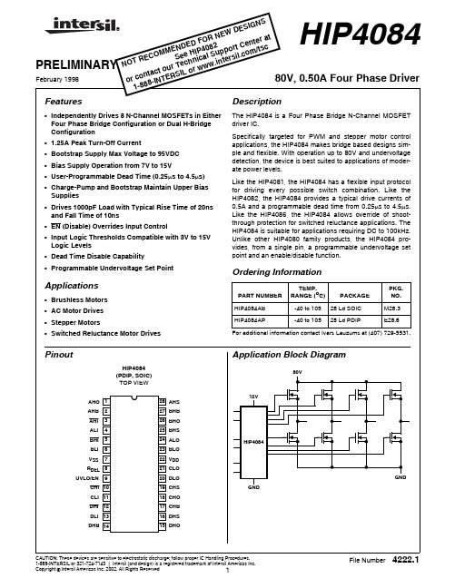
• Independently Drives 4 N-Channel FET in Half Bridge or Full Bridge Configurations
• Bootstrap Supply Max Voltage to 95VDC
• Drives 1000pF Load in Free Air at 50°C with Rise and Fall Times of Typically 15ns
元器件交易网
HIP4082
Typical Application (PWM Mode Switching)
12V PWM INPUT DELAY RESISTOR
DIS
1 BHB 2 BHI 3 BLI 4 ALI 5 DEL 6 VSS 7 AHI 8 DIS
BHO 16 BHS 15 BLO 14 ALO 13
9 AHB BHB 1
DRIVER
DRIVER
10 AHO BHO 16
11 AHS BHS 15
LEVEL SHIFT
U/V
TURN-ON DELAY
TURN-ON DELAY
VDD
DRIVER
DRIVER
13 ALO BLO 14
TURN-ON DELAY
2
FN3676.4
January 3, 2006
Voltage on AHS, BHS . . . . . -6V (Transient) to 70V (-55°C to150°C)
Voltage on AHB, BHB . . . . . . . . VAHS, BHS -0.3V to VAHS, BHS +VDD Voltage on ALO, BLO. . . . . . . . . . . . . . . . . . VSS -0.3V to VDD +0.3V Voltage on AHO, BHO . . . VAHS, BHS -0.3V to VAHB, BHB +0.3V Input Current, DEL . . . . . . . . . . . . . . . . . . . . . . . . . . . . . . . . -5mA to 0mA
海康威视HiPAP HPR 400系统二进制通信协议说明书
HPR 400 Binary Communication Protocol This document describes the binary telegrams transmitted from the Operator Station in the HiPAP / HPR 400 systems. It also describes some of the ASCII sentences transmitted from and received by the Operator Station.The ASCII sentences complying with the NMEA 0183 rules are described in the APOS on-line helpDocument revisions Documentation Department Hardware/Software design Project/ProductManagementRev Date Sign Date Sign Date Sign A10.03.98 GM 24.07.98 HJP 03.08.98 JEF B15.05.03 GM 15.05.03 THG 15.05.03 JEF C03.05.04 GM 06.05.04 THG 06.05.04 JEF D(The original signatures are recorded in the company’s logistic database.)Contents1INTRODUCTION (5)1.1Definitions (5)2GENERAL TELEGRAM FORMAT (7)2.1Time of telegram transmission (8)2.2Floating point data format (8)2.3Serial line format (9)2.4Ethernet format (9)2.5ADP Ethernet header (9)3TELEGRAMS SENT FROM THE OPERATOR STATION (10)3.1Message 1, Transponder position data (10)Example (14)3.2Message 2, LBL position (15)Time Header (18)Example (18)3.3Message 4, LBL Ranges (19)Document history(The information on this page is for internal use)Rev. A Original issue.Earlier, the HPR 400 binary protocol document was distributed as anunofficial document, not included in the manuals. The last unofficialdocument was "Communication Protocol V2.1" - file name SWTS013.H /94.11.17.Rev. B Updated the Message 2, LBL position - Pos_north. Removed sections 3.4 /3.5 / 3.6 and chapter4.Rev. C Updated layout. Miner corrections in the text.1 INTRODUCTIONThis note is a technical documentation that may be changed. Pleasecontact Kongsberg Maritime before implementing the reception oftelegrams to assure that the note matches the SW version in the actualHiPAP/HPR system to be interfaced.1.1 DefinitionsThe following abbreviations are used in this document:APOS A coustic Positioning Operator Station, the “new” OperatorStation.BYTE 8 bit dataHiPAP High Precision Acoustic PositioningHPR Hydroacoustic Positioning Reference systemHSC 400HPR 400 System Controller, the “old” Operator Station.LBL Long Base Linems MillisecondsREAL 32 bit floating point dataREAL_64 64 bit floating point dataROV Remotely Operated VehicleSSBL Super Short Base LineTD TransducerTP TransPonderWORD_16 16 bit dataAPOS is the Acoustic Positioning Operator Station with Windows.All telegrams are implemented in the APOS.HPR 400 and HiPAP are two different types of transceivers. Theymay both be connected to an APOS Operator Station. The telegramsare delivered by the Operator Station, and the format is independent ofthe physical units involved.Later in the note, the term The system means the HiPAP / HPR 400system. The term The Operator Station is used for APOS.The binary telegrams and the ASCII sentences are the transmitted tothe Com ports and to the Ethernet as specified in the configurationmenus in the Operator Station. The same telegram may be configuredto be sent to many, to one or to none destinations.The following “terms” are used:X - POSITION Athwart ship distance to transponder, positivedirection towards starboard.Y - POSITION Fore and Aft ship distance to transponder,positive direction forward.Z - POSITION The transponder depth, positive directiondownwards.SLANT RANGE The distance to the transponder.COURSE Vessels heading, 0 - 360 degrees, positivedirection turning clockwise.ROLL Vessels roll, -180 -, 0, - 180 degrees, positivedirection is vessels port side up.PITCH Vessels pitch, -180 -, 0, - 180 degrees, positivedirection is bow up.Positive vessel y-axis is forward, positive vessel x axis is towards starboard and positive vessel z-axis is downwards. This is a left-hand coordinate system.2 GENERAL TELEGRAM FORMATThe binary telegrams transmitted on asynchronous serial lines followthe same general format with telegram heading and telegram tail. Thecontent of the data block depends on the message type, as describedfor each message.The telegrams transmitted on Ethernet have another heading, asdescribed in 2.4 and 2.5.Index Content Sizecharacter BYTE000 Start001 Block length N WORD_16type BYTE003 Message004 Destination BYTE005 Data Block with N bytesN+5 Sumcheck WORD_16character BYTEN+7 StopStart character The start character is 55 hex.Block length The block length defines the length of the data block.Message type The message type defines the message transmitted. It is a numberbetween 1 and 255.Destination The destination defines the device to which this telegram istransferred. It is not in use, and it is always set to 0.Data block The data block contains the message itself.The length N depends on the Message type. The data block for thedifferent message types are explained in the next chapters.Sumcheck The sumcheck is the 16 bit sum of all bytes in the telegram, exceptthe sumcheck itself and the stop character. The sum is calculated bybyte+byte addition.Stop character The stop character is equal to 0AAH.Note !The start character and the stop character are not unique. They mayalso occur as data within the telegram.2.1 Time of telegram transmissionThe time delay between the end of one telegram and the start of thenext one is at least 30 ms. It separates the telegrams.2.2 Floating point data formatBoth 32 bits and 64 bits floating formats are used in the telegrams.They are coded according to the IEEE standard 754. 32 bits floatingnumbers use the single precision data format. They are named REALthroughout the note. 64 bits floating numbers use the double precisiondata format. They are named REAL_64 throughout the note.The REAL format occupies 4 contiguous bytes of memory,(32 bits).SIGN EXPONENT SIGNIFICANT31 30 23 22 0Sign Sign = 0 if value is positive or zeroSign = 1 if value is negative.Exponent The exponent field contains a value offset by 127. The actualexponent can be obtained from the exponent field by subtracting127. The field is zero if the REAL value is zero.Significant The byte with the lowest address contains the least significant 8 bitsof the significant, and the byte in the highest address contains the signand the 7 most significant bits of the exponent.The REAL_64 format occupies 8 contiguous bytes of memory asshown below. The explanation of the fields is similar to theexplanation for REAL, except that the exponent is biased with 1023instead of 127.SIGN EXPONENT SIGNIFICANT63 62 52 51 02.3 Serial line formatThe serial line format is:Baud rate: Selectable between 300 and 38400 baud.The default value is 9600 baud.Parity: noneData bits: 8Stop bits: 1The least significant byte (bit 0-7) is transmitted first in bothWORD_16s, REALs and REAL_64s, followed by the moresignificant bytes.2.4 Ethernet formatWhen the telegrams are sent to external units via Ethernet, they aresent as an UDP message. They can be sent as individual messages oras broadcast messages.The telegram contains the "Message type" and the "Data Block" inaddition to the UDP blocks.Index Content Size0 Messagetype BYTE1 Data block with N bytesThe meaning of the "Message Type" and the "Data Block" is asdescribed in the start of the chapter for the serial lines.2.5 ADP Ethernet headerThe Kongsberg Maritime ADP header consists of 16 bytes. Theyreplace the message type in the normal header explained above. TheKongsberg Maritime ADP header is only used when explicitlyrequested in the Operator Station menus.3 TELEGRAMS SENT FROM THE OPERATORSTATION3.1 Message 1, Transponder position dataThe position message telegram contains SSBL transponder positiondata and sensor data related to the position measurement. It istransmitted each time a new position is calculated.Block content SizeTp_index WORD_16Operation_mode BYTESync_mode BYTETp_type BYTETp_operation BYTEPos_data_form BYTEReply_status BYTEFilt_X_pos REALFilt_Y_pos REALFilt_Z_pos REALX_pos REALY_pos REALZ_pos REALSlant_range REALP_course REALP_roll REALP_pitch REALTd_beam BYTETd_type BYTETd_num WORD_16Diagnostic WORD_16Stand_dev REALInstr_data (*) REALTp_index defines the Tp for which the position is valid.It is a number from 1 to 298. The indexes below 100 are for the lowfrequency Tps (The Axx Tps), the indexes between 100 and 200 arefor the medium frequency Tps (The Bxx Tps), and the indexesbetween 200 and 298 are for the high frequency Tps (The Cxx Tps).Examples: A02 is coded with Tp_index 2.B01 --“-- 101.B56 --“-- 156.Operation_mode Contains the Operation mode of the transceiver.00 equals standard navigation mode.01 " simulated position test mode. (Training)Sync_mode Contains the synchronization mode of the transceiver.0 equals No synchronization.1 " Sequence sync.2 " Interrogation sync.Tp_type Defines the transponder type:000 equals transpondertransponder001 " depthtransponder002 " inclinometer003 " diff. incl. transpondertransponder004 " compass005 " acoustic control transponder006 " beaconbeacon007 " depth010 " responder drive 1011 " responder drive 2012 " responder drive 3013 " responder drive 4Tp_operation Defines the operation mode of the transponder:000 equals fixed standard transponder-------"-----------001 " mobilePos_data_form Defines the position coordinate format:Bit 0 = 0 vessel oriented, cartesian.Bit 0 = 1 north oriented, cartesian.Bit 3 = 1 Ping count data validThe coordinates are normally vessel oriented, that is bit 0 is 0.Reply_status Defines the transponder reply status. When the whole byte is zero, thereply is ok.Bit 0 and 1 contains information about timeouts.Value 1 means timeout on the first pulse, value 2 meanstimeout on the second pulse and value 3 means timeouton the third pulse.Bit 2 set Ambiguity error X angle.Bit 3 set Ambiguity error Y angle.Bit 4 set Reply rejected by the software filter.Bit 5 set VRU or gyro error. The position is calculated with zerocourse and/or zero roll and pitch. The VRU and/or gyroerror is reported in the DIAGNOSTIC parameter.Filt_X_pos The filtered x - position coordinates of the transponder. Transpondershorizontal athwart ship distance from reference point. A meter valuein REAL format.Filt_Y_pos The filtered y - position coordinates of the transponder. Transpondershorizontal fore and aft ship distance from reference point. A metervalue in REAL format.Filt_Z_pos: (Depth) The filtered z - position coordinates of the transponder. Transpondersvertical distance from reference point. A meter value in REALformat.X_pos The raw x - position coordinates of the transponder. Transpondershorizontal athwart ship distance from reference point. A meter valuein REAL format.Y_pos The raw y - position coordinates of the transponder. Transpondershorizontal fore and aft ship distance from reference point. A metervalue in REAL format.Z_pos: (Depth) The raw z - position coordinates of the transponder. Transpondersvertical distance from reference point. A meter value in REALformat.Slant_range The direct raw slant range from the vessel's transducer to thetransponder. A meter value in REAL format.P_course The vessels course at the time of transponder position measurement.A value in REAL format, 0 to 360 degrees.P_roll The vessels roll at the time of transponder position measurement. Avalue in REAL format, +/-180 degrees.P_pitch The vessels pitch at the time of transponder position measurement. Avalue in REAL format, +/-180 degrees.Td_beam Defines the transducer beam, 0=wide, 1=narrow.Td_type defines the transducer type.0 equals 30 kHz wide beam only1 " 30 kHz wide/medium beam2 " 30 kHz wide/narrow beam3 " 30 kHz PMT-300, wide/wide extendedbaseline.wide/medium4 " 15kHzLBLkHz5 " 30LBL6 " 15kHz7 " 30 kHz SSBL NMT-3018 " 30 kHz SSBL tracking td-erkHzHiPAP9 " 30Td_num defines the transducer number 1 to 4 used in the positioning.Diagnostic Defines the transceiver hardware status.Error information Error index15 87 0The least significant byte of this WORD_16 parameter contains anindex, defining one error. If there is more than one error, the indexwill alter between the error indexes. The most significant byte of theparameter contains additional information for the error reported bythe index.The error indexes are reserved according to the following plan:1 to 31 General errors32 to 63 Application specific errors64 to 255 Debug diagnostics.The General errors are:reset1 HW2 Fatal transceiver errorerror3 VRUerror4 Gyro5 External serial line error6 Transmittererrorerror7 DSP8Tracking td errorWhen the Operator unit receives an error index, it is displayedtogether with the additional information. The additional informationis displayed as a hex number. The meaning of the numbers isexplained in the Operator's manual.Stand_dev The expected accuracy of the position. It is based on the covariance data calculated for the SSBL position. It is equal to the statistical sumof the major and minor semi axes of the error ellipse displayedaround the position.Instr_data (*) This is only used if any of the below cases are true:If the message contains data from a Inclinometer transponder,( Tp_type = 2 or 3 ), the first two reals contain the Inclination of thetransponder. The first contains X inclination and the second containsthe Y inclination.If the message contains data from a compass transponder,( Tp_type = 4 ), the first real in Instr_data contains the heading of thecompass transponder.If the message contains data from a depth transponder,( Tp_type = 1), the first real in Instr_data contains the depthmeasured by the transponder.If bit 3 in Pos_data_form is set, the first real in Instr_data contains theping count from the transponder with resolution million ping.If Td_type is tracking td, the last real value contains the tracking tdangle.E xampleTelegram:55 3a 00 01 00 94 00 01 00 00 00 00 00 fc e4 c9 42 72 46 6e c247 cd 80 40 bb ed c9 42 25 85 6e c2 c2 cc 8c 40 80 5b e8 42 0000 00 00 00 00 00 00 00 00 00 00 01 01 02 00 00 00 58 5c 00 40b0 11 aaThe data block of the telegram decoded:TpOmSmTtToPfSt X Y Z148 1 0 0 0 0 0 100.95 -59.57 4.03100.96 -59.63 4.40Rang Crs Roll Pitc TbTtT#Diag Std116 0.0 0.00 0.00 1 1 2 0 2.013.2 Message 2, LBL positionThe LBL position telegram contains a position relative to the origin ofthe Tp array. The position is of the vessel or of another object. Thetelegram is transmitted each time a new position is calculated. If theTransponder array is north oriented, the coordinates are relative to trueNorth, else they are relative to local north.Block content SizeSequence_number WORD_16Time_header (7) BYTEInterrogation_age WORD_16Tp_array BYTETd_num BYTEPos_east REAL_64Pos_north REAL_64Depth REALHor_err_ellipse_direction REALHor_err_ellipse_major REALHor_err_ellipse_minor REALZ_standard_deviation REALPos_type BYTEPos_status BYTEP_course REALP_roll REALP_pitch REALDiagnostic WORD_16 Sequence_number The sequence number is incremented for each LBL interrogation. It isreset each time LBL positioning is started. Range 0 - 65535.Time_header See subchapter below.Interrogation_age Time since interrogation of transponder array. The resolution is 1ms.Tp_array When the LBL position is calculated in Navigation mode, it containsthe Tp array number in use (1 and upwards).When the position is calculated in Training mode, it contains 255.Td_num Defines the transducer number in use.1 to 4 means td 1 to 4 on transceiver 15 to 8 " 29 to 12 " 313 to 16 " 40 has a special meaning. Then the position is calculated based onmeasurements on more than one transducer.Pos_east Pos_north The East and North coordinate of the position in meters. Positive East value is towards east, and positive North value is towards north.The coordinates are local coordinates.The HSC 400 also includes global UTM coordinates.Depth The depth coordinate in meters. Positive value is downwards.It is the vertical distance from the sea level to the reference point ofthe object being positioning.Hor_err_ellipse_direction Each LBL position has an one sigma error ellipse associated with it. The direction is the angle in degrees between the north axis and the major axis of the ellipse.Hor_err_ellipse_majorThe major semi axis of the error ellipse.Hor_err_ellipse_minorThe minor semi axis of the error ellipse.Z_standard_deviationThe standard deviation of the depth.Pos_type 0 - Position of the vessel1 - Position of ROV1: :16 - Position of ROV1617 - Position of TP range Position no 1: :20 - Position of TP range Position no 4Bit 7 is 0 if the coordinates are local. It is set if the they are UTMcoordinates.Pos_status This variable tells the status of the position calculation. The statuses with an asterisk in the table below are so serious that no position iscontained in the telegram.position.0 Ok1 The measured ranges match badly the calculated position. Therange residuals are big.2The position calculation did converge in the horizontal plane, but not vertically.3The calculation of the interrogation time in MuLBL mode didnot converge.16* Too few ranges are measured.17* The position calculation does not converge.18* Internal HPR computation error.19* No initial position is calculated.P_course An average of course read at the time of pulse arrival.P_roll An average of roll read at the time of pulse arrival.P_pitch An average of pitch read at the time of pulse arrival.Diagnostic See Message 1, Transponder position data.T ime HeaderThe format of the Time_header is:BlockcontentSize Index Resolution Range Day BYTE1Day1-31 Month BYTE11Month1-12 Year BYTE21Year0-99 Hours BYTE31Hour0-23 Minutes BYTE 41Minute0-59 Seconds BYTE 5 1 Second 0-591/100th seconds BYTE 6 1/100second0-100It defines the clock when the position is valid.E xampleTelegram:55 41 00 02 00 08 00 18 07 62 0d 2b 23 4a f8 0a ff 02 7a a5 cf f8 d3 fc 68 40 3d e2 a3 fb 5d 14 59 c0 70 01 9c c0 ef b3 a8 41 ff 3a 07 3e da a1 fc 3d ca 39 18 3e 00 00 00 00 00 00 00 00 00 00 00 00 00 00 00 00 50 17 aaThe data block of the telegram decoded:Seqno ddmmyyhhmmss.hh Age Ar Td East8 240798134335,74 2808 ff 2 199.90North Depth Dir Major Minor Dsigm Pt Ps-100.32 -4.88 21 0.13 0.12 0.15 0 0Crs Roll Pitch Diag0.0 0.00 0.00 03.3 Message 4, LBL RangesThe LBL_ranges message contains raw measured ranges to thetransponders, and VRU and compass data. This Message istransmitted just after the Message 2 (LBL position). The twomessages have the same sequence number.Block content SizeSequence_number WORD_16Range_age (8) WORD_16Tp_array BYTETd_num BYTEOperation_mode BYTESync_mode BYTEPos_type BYTEReply_status (8) BYTERange (8) REALP_course REALP_roll REALP_pitch REALDiagnostic WORD_16Range_age, reply_status and range consist of a list with 8 entries, onefor each transponder.Sequence_number The sequence number is incremented for each LBL interrogation. It isreset each time LBL positioning is turned ON. Range 0 - 65535.Range_age Time since reception of the range. Resolution 1ms.Tp_array When the LBL position is calculated in Navigation mode, it containsthe Tp array number in use (1 and upwards).When the position is calculated in Training mode, it contains 255.Td_num Defines the transducer number in use.1 to 4 means td 1 to 4 on transceiver 15 to 8 " 29 to 12 " 313 to 16 " 4Operation_mode See Message 1, Transponder position data.Sync_mode contains the synchronization mode of the transceiver.0 equals No synchronization.1 " Sequence sync.2 " Interrogation sync.Pos_type 0 - Position of the vessel1 - Position of ROV1: :16 - Position of ROV1617 - Position of TP range Position no 1: :20 - Position of TP range Position no 4Reply_status_n Defines the reply status. When bit 0 to 5 are zero, the measurement is OK.Bit 0 and 1 contains information about timeouts.Value 1 means timeout on the first pulse, value 2 meanstimeout on the second pulse and value 3 means timeouton the third pulse.Bit 2 set Ambiguity error or angle rejected X angle.Bit 3 set Ambiguity error or angle rejected Y angle.Bit 4 set Range rejected by the software filter.Bit 5 set Vru or gyro error. The position is calculated with zerocourse and/or zero roll and pitch. The VRU and/or gyroerror is reported in the DIAGNOSTIC parameter.Bit 6 and 7 contain information about what is measured. The contentsof the two bits are either 00 (no measurement), 80H (only the range ismeasured) or C0H (both the range and the directions are measured).Bit 7 set The range is measured OK.Bit 6 set The SSBL directions are measured OK.Range_n The measured range to the transponders.P_course An average of course read at the time of pulse arrival.P_roll An average of roll read at the time of pulse arrival.P_pitch An average of pitch read at the time of pulse arrival.Diagnostic See Message 1, Transponder position data.。
pic24各个模块数据手册(中文)2章cpu
© 2007 Microchip Technology Inc.
超前信息
DS39703A_CN 第 2-1 页
PIC24F 系列参考手册
2.1
简介
PIC24F CPU 模块采用 16 位(数据)改良的哈佛架构,并带有增强型指令集。CPU 具有 24 位指令 字,指令字带有长度可变的操作码字段。程序计数器(Program Counter,PC)为 24 位宽,可以寻 址高达 4M x 24 位的用户程序存储空间。单周期指令预取机制用来帮助维持吞吐量并提供可预测 的指令执行过程。除了改变程序流的指令、双字移动 (MOV.D)指令和表指令以外,所有指令都 在单个周期内执行。模块使用 REPEAT 指令支持无开销的程序循环结构,该指令在任何时候都可 被中断。
指令集架构 (Instruction Set Architecture, ISA)在 PIC18F 指令集架构的基础上有显著增强, 但仍在可接受程度上保持了向后兼容性。所有 PIC18F 指令和寻址模式都能直接得到支持或通过 简单的宏得到支持。许多 ISA 增强功能都是为了提高编译器效率而做出的。
内核支持固有(无操作数)、相对、立即数和存储器直接寻址模式,以及 3 组寻址模式(MODE1、 MODE2 和 MODE3)。所有模式都支持寄存器直接和各种寄存器间接寻址模式。每组都提供最多 7 种寻址模式。指令根据其功能要求,与预定义的寻址模式相关联。
PIC24F 指令集可被分成两种指令类型:寄存器和文件寄存器指令。寄存器指令可以把每个 W 寄 存器用作数据值或地址偏移值。例如:
例 2-1:
寄存器指令
MOV
W0, W1
; move contents of W0 to W1
MOV
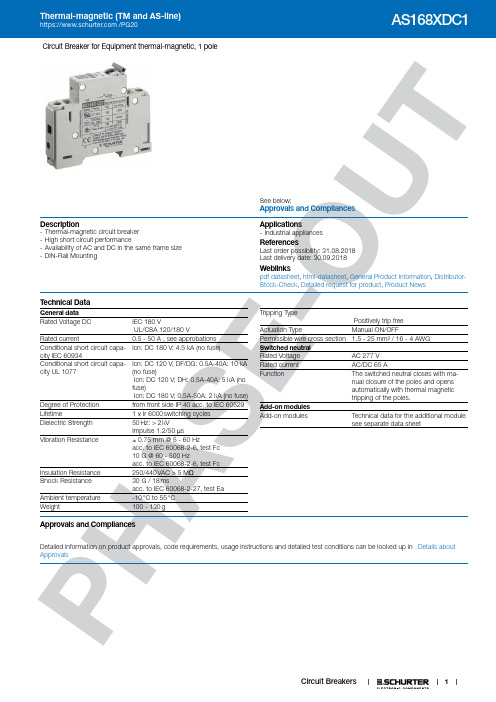
Schurter PG20 电路保护器数据手册说明书
1P HA SE -O UTCircuit Breaker for Equipment thermal-magnetic, 1 poleSee below:Approvals and Compliances Description- Thermal-magnetic circuit breaker - High short circuit performance- Availability of AC and DC in the same frame size - DIN-Rail MountingApplications - Industrial appliancesReferences Last order possibility: 31.08.2018Last delivery date: 30.09.2018Weblinkspdf datasheet , html-datasheet , General Product Information , Distributor-Stock-Check , Detailed request for product , Product NewsT echnical DataGeneral data Rated Voltage DCIEC 180 VUL/CSA 120/180 VRated current 0.5 - 50 A , see approbations Conditional short circuit capa-city IEC 60934Icn: DC 180 V: 4.5 kA (no fuse) Conditional short circuit capa-city UL 1077Icn: DC 120 V; DF/DG: 0.5A-40A: 10 kA (no fuse)Icn: DC 120 V; DH: 0.5A-40A: 5 kA (no fuse)Icn: DC 180 V; 0.5A-50A: 2 kA (no fuse)Degree of Protection from front side IP 40 acc. to IEC 60529Lifetime 1 x Ir 6000 switching cycles Dielectric Strength 50 Hz: > 2 kVImpulse 1.2/50 μsVibration Resistance ± 0.75 mm @ 5 - 60 Hzacc. to IEC 60068-2-6, test Fc 10 G @ 60 - 500 Hzacc. to IEC 60068-2-6, test FcInsulation Resistance 250/440 VAC > 5 M ΩShock Resistance 30 G / 18 msacc. to IEC 60068-2-27, test EaAmbient temperature -10 °C to 55 °C Weight 100 - 130 gTripping TypePositively trip freeActuation Type Manual ON/OFFPermissible wire cross section 1.5 - 25 mm² / 16 - 4 AWG Switched neutral Rated Voltage AC 277 V Rated current AC/DC 65 A Function The switched neutral closes with ma-nual closure of the poles and opensautomatically with thermal magnetic tripping of the poles.Add-on modules Add-on modules Technical data for the additional modulesee separate data sheetApprovals and CompliancesDetailed information on product approvals, code requirements, usage instructions and detailed test conditions can be looked up in Details about Approvals2P HA SE -O U TApprovalsThe approval mark is used by the testing authorities to certify compliance with the safety requirements placed on electronic products. Approval Reference T ype: AS168XApproval LogoCertificates Certification Body DescriptionVDE Approvals VDEVDE Certificate Number: 40005743UL Approvals UL UL File Number: E216629 / E71572UL Approvals ULUL File Number: E216629 / E71572CQC ApprovalsCQCCCC Certificate Number: 2013010307594187Product standardsProduct standards that are referencedOrganizationDesignStandardDescriptionDesigned according to IEC 60934Circuit-breakers for equipment (CBE)Designed according to UL 1077Standard for Supplementary Protectors for Use in Electrical Equipment Designed according toCSA C22.2Supplementary Protectors Application standardsApplication standards where the product can be usedOrganizationDesignStandardDescriptionDesigned for applications acc.IEC/UL 60950IEC 60950-1 includes the basic requirements for the safety of information technologyequipment.CompliancesThe product complies with following Guide LinesIdentificationDetailsInitiatorDescriptionCE declaration of conformitySCHURTER AG The CE marking declares that the product complies with the applicable requirements laid down in the harmonisation of Community legislation onits affixing in accordance with EU Regulation 765/2008.RoHSSCHURTER AGEU Directive RoHS 2011/65/EUChina RoHS SCHURTER AG The law SJ / T 11363-2006 (China RoHS) has been in force since 1 March2007. It is similar to the EU directive RoHS.REACHSCHURTER AGOn 1 June 2007, Regulation (EC) No 1907/2006 on the Registration, Evaluation, Authorization and Restriction of Chemicals 1 (abbreviated as "REACH") entered into force.PDimension [mm]AS168X 1 poleA) 35 mm DIN rail EN 50022B) Max. torqueWire crosssection Max. torque1.5 ... 10 mm22.5 Nm16 ... 25 mm2 3.1 NmAWG #16 ... 8 20 ... 22 lb–inAWG #6 ... 4 26 ... 28 lb–inAS168X 1 pole and switched neutral poleA) 35 mm DIN rail EN 50022B) Max. torqueWire crosssection Max. torque1.5 ... 10 mm22.5 Nm16 ... 25 mm2 3.1 NmAWG #16 ... 8 20 ... 22 lb–inAWG #6 ... 4 26 ... 28 lb–in34PHS-U Diagrams AS168X-CB1...AS168X-CB1...NAS168X-CB1... / AS168X-ACBH1AS168X-CB1... / AS168X-ACBH2AS168X-CB1... / AS168X-ACBS1AS168X-CB1... / AS168X-ACBS2AS168X-CB1... / AS168X-ACBA5P-U Effect of ambient temperatureAC-breaker are calibrated for an ambient temperature of +40°C, DC-breakers for +23°C. To determine the rated current for a lower or Time-Current-Curves Version DF / Magnetic 4.5-8 xl nT i m e i n S e c o n d snMultiple of Rated Current InReference Temperature +23°Version DG / Magnetic 9-16 xl nT i m e i n S e c o n d snMultiple of Rated Current InReference Temperature +23°6A-O U TVersion DH / Magnetic 18-32 xl nT i m e i n S e c o n d sn0,1ms1ms10ms0,1s1s10s100sMultiple of Rated Current InReference Temperature +23°Config. CodeAS168X-CB 1DG |200|N |The characters are placeholders for the correspondingly keys of selections from the key tables.AS168X-CB 1 DG |200|N | = Number of PolesAS168X-CB |1| DG |200|N | = Tripping characteristicsAS168X-CB |1|DG | 200 |N | = Rated currentAS168X-CB |1|DG |200| N | = Switched neutral7P HA SE -O U VariantsPackaging Unit 1 PcsThe specifications, descriptions and illustrations indicated in this document are based on currentinformation. All content is subject to modifications and amendments. Information furnished is believed 19.02.2018。
HIP4084中文资料
CAUTION: These devices are sensitive to electrostatic discharge; follow proper IC Handling Procedures.1-888-INTERSIL or 321-724-7143Intersil (and design) is a registered trademark of Intersil Americas Inc.File NumberTRUTH TABLEINPUT OUTPUTALI, BLI, CLI, DLI AHI, BHI, CHI, DHI UVLO/EN R DEL ALO, BLO,CLO, DLOAHO, BHO,CHO, DHOX X0X00 1X1>100mV10 001X01 011X00 101<100mV11 NOTE:X signifies that input can be either a “1” or “0”.Pin DescriptionsPINNUMBER SYMBOL DESCRIPTION2 27 17 14AHBBHBCHBDHB(xHB)High-side Bootstrap supplies. One external bootstrap diode and one capacitor are required for each. Connect cathode of bootstrap diode and positive side of bootstrap capacitor to each xHB pin.3 5 10 12AHIBHICHIDHI(xHI)High-Side Logic Level Inputs. Logic at these three pins controls the three high-side output drivers, AHO (Pin 1), BHO (Pin 26) and CHO (Pin 18) and DHO (Pin 15). When xHI is low, xHO is high. When xHI is high, xHO is low.Unless the dead time is disabled by connecting R DEL (Pin 8) to ground, the low side input of each phase will override the corresponding high side input on that phase. If R DEL is tied to ground, dead time is disabled and the outputs follow the inputs. Care must be taken to avoid shoot-through in this application. EN (Pin 9) also over-rides the high side inputs. xHI can be driven by signal levels of 0V to 15V (no greater than V DD). An internal 100µA pull-up to V DD will hold each xHI high if the pins are not driven.4 6 11 13ALIBLICLIDLI(xLI)Low-Side Logic Level Inputs. Logic at these three pins controls the three low-side output drivers ALO (Pin 24), BLO (Pin 23) and CLO (Pin 21) and DLO (Pin 20). If the upper inputs are grounded then the lower inputs controls both xLO and xHO drivers, with the dead time set by the resistor at R DEL (Pin 8). EN (Pin 9) high level input overrides xLI, forcing all outputs low. xLI can be driven by signal levels of 0V to 15V (no greater than V DD). An internal 100µA pull-up to V DD will hold xLI high if these pins are not driven.7V SS Ground. Connect the sources of the low-side power MOSFETs to this pin.8R DEL Dead Time Setting. Connect resistor from this pin to V DD to set timing current that defines the dead time be-tween drivers. All drivers turn-off with no adjustable delay, so the R DEL resistor guarantees no shoot-through bydelaying the turn-on of all drivers. When R DEL is tied to V SS, both upper and lowers can be commanded onsimultaneously. While not necessary in most applications, a decoupling capacitor of 0.1µF or smaller may beconnected between R DEL and V SS.9RUV/EN A resistor can be connected between this pin and V SS to program the under voltage set point. With this pin not connected the undervoltage setpoint is typically 6.6V. When this pin is tied to V DD, the undervoltage setpoint istypically 6.2V. With this pin tied to V SS, all six outputs are taken low, overriding all other inputs.1 26 18 15AHOBHOCHODHO(xHO)High-Side Outputs. Connect the gates of the high-side power MOSFETs to these pins.28 25 19 16AHSBHSCHSDHS(xHS)High-Side Source connection. Connect the sources of the high-side power MOSFETs to these pins. The nega-tive side of the bootstrap capacitors should also be connected to these pins.22V DD Positive supply. De-couple this pin to V SS (Pin 7).24 23 21 20ALOBLOCLODLO(xLO)Low-Side Outputs. Connect the gates of the low-side power MOSFETs to these pins.NOTE:x = A, B, C and DAbsolute Maximum Ratings T A=25o C Thermal InformationSupply Voltage, V DD . . . . . . . . . . . . . . . . . . . . . . . . . . -0.3V to 16V Logic I/O Voltages . . . . . . . . . . . . . . . . . . . . . . .-0.3V to V DD +0.3V Voltage on xHS. . . . . . . . .-6V (Transient) to +85V (-40o C to 150o C) Voltage on xHB. . . . . . . . . . . . . . . . . . . . .V xHS -0.3V to V xHS +V DD Voltage on xLO. . . . . . . . . . . . . . . . . . . . . . V SS -0.3V to V DD +0.3V Voltage on xHO . . . . . . . . . . . . . . . . . . . .V xHS -0.3V to V xHB +0.3V Phase Slew Rate . . . . . . . . . . . . . . . . . . . . . . . . . . . . . . . . . .20V/ns Operating ConditionsSupply Voltage, V DD . . . . . . . . . . . . . . . . . . . . . . . . .+7.0V to +15V Voltage on V xHS. . . . . . . . . . . . . . . . . . . . . . . . . . . . . . . . .0V to 80V Voltage on xHB. . . . . . . . . . . . . . . . . . . . . . . . . . . . . . . .V xHS + V DD Thermal Resistance (Typical, Note 1)θJA (o C/W) SOIC Package. . . . . . . . . . . . . . . . . . . . . . . . . . . . . 75o C PDIP Package. . . . . . . . . . . . . . . . . . . . . . . . . . . . . 65o C Maximum Junction Temperature. . . . . . . . . . . . . . . . . . . . . . .150o C Maximum Storage Temperature Range . . . . . . . . . .-65o C to 150o C Maximum Lead Temperature (Soldering 10s). . . . . . . . . . . . .300o C (SOIC - Lead Tips Only)Operating Ambient Temperature Range. . . . . . . . . .-40o C to 105o C Operating Junction Temperature Range . . . . . . . . .-40o C to 105o CCAUTION: Stresses above those listed in “Absolute Maximum Ratings” may cause permanent damage to the device. This is a stress only rating and operation of the device at these or any other conditions above those indicated in the operational sections of this specification is not implied.NOTES:1.θJA is measured with the component mounted on an evaluation PC board in free air.2.All voltages are relative to VSS unless otherwise specified.3.x = A, B, C, and D. For example, xHS refers to AHS, BHS, CHS, and DHS.Electrical Specifications V DD = V xHB = 12V, V SS = V xHS = 0V, R DEL = 20K, UVLO/EN = ∞, Gate Capacitance (C GATE) = 1000pFPARAMETER TEST CONDITIONST J = 25o CT J = -40o C TO150o CUNITS MIN TYP MAX MIN MAXSUPPLY CURRENTS AND UNDER VOLTAGE PROTECTIONV DD Quiescent Current xHI=5V,xLI=5V34526mA V DD Operating Current f = 20kHz, 50% Duty Cycle89.512713 mA xHB On Quiescent Current xHI = 0V-4080-100µA xHB Off Quiescent Current xHI = V DD0.60.8 1.30.5 1.4mA xHB Operating Current f = 20kHz, 50% Duty Cycle0.70.9 1.3 2.0mA Q PUMP Output Voltage No Load11.512.51410.514.5V Q PUMP Output Current V xHB = 10V-100130-140µA xHB, xHS Leakage Current V xHS = 80V, V xHB = 93V72445-50µA V DD Rising Undervoltage Threshold R UV Open 6.27.18.0 6.18.1V V DD Falling Undervoltage Threshold R UV Open 5.75 6.67.5 5.67.6V Minimum Undervoltage Threshold R UV = V DD5 6.2 6.8 4.9 6.9V INPUT PINS: ALI, BLI, CLI, DLI, AHI, BHI, CHI, DHI, AND ENLow Level Input Voltage-- 1.0-0.8V High Level Input Voltage 2.5-- 2.7-V Input Voltage Hysteresis-35---mV Low Level Input Current V IN = 0V6010013555140µA High Level Input Current V IN = 5V-1-1-1010µA GATE DRIVER OUTPUT PINS: ALO, BLO, CLO, DLO, AHO, BHO, CHO, AND DHOLow Level Output Voltage (V OUT-V SS)I SINKING = 30mA-100--200mV Peak Pulse Pullup Current V OUT 0V to 5V0.30.50.7- 1.0APeak Pulse Pulldown CurrentV OUT 12V to 4V0.71.11.50.51.7ASwitching Specifications V DD = V xHB = 12V, V SS = V xHS = 0V, R DEL = 10K, Gate Capacitance (C GATE ) = 1000pFPARAMETERTEST CONDITIONST J = 25o CT J = -40o C TO150o C UNITSMINTYPMAXMINMAXTURN ON DELAY AND PROPAGATION DELAY Dead TimeR DEL = 100K 3.8 4.5637µs R DEL = 10K0.380.50.650.30.7µs Dead Time Channel Matching R DEL = 10K -715-20%Lower Turn-Off Propagation Delay (xLI-xLO)No Load-2550-70nsUpper Turn-Off Propagation Delay (xHI-xHO)No Load -5580-100nsLower Turn-On Propagation Delay (xLI-xLO)No Load -4085-100nsUpper Turn-On Propagation Delay (xHI-xHO)No Load -75110-150nsRise Time C GATE = 1000pF -2040-50ns Fall TimeC GATE = 1000pF-1020-25ns Turn-On Input Pulse Width 50--50-ns Turn-Off Input Pulse Width50--50-ns Disable (EN) Turn-Off Propagation Delay (EN - xLO)-508090nsDisable (EN) Turn-Off Propagation Delay (EN - xHO)-75100-125nsEnable to Lower Turn-On Propagation Delay (EN - xLO)-5080-100nsEnable to Upper Turn-On Propagation Delay (EN- xHO)R DEL = 10K - 1.22-3µsRefresh Pulse Width (xLO)375580900350950µsElectrical SpecificationsV DD = V xHB = 12V, V SS = V xHS = 0V, R DEL = 20K, UVLO/EN = ∞, Gate Capacitance (C GATE ) = 1000pFPARAMETERTEST CONDITIONS T J = 25o CT J = -40o C TO150o C UNITS MIN TYP MAX MIN MAX。
HIP4082IP中文数据手册

1-888-INTERSIL or 1-888-468-3774
| Intersil (and design) is a registered trademark of Intersil Americas Inc.
Copyright Harris Corporation 1995. Copyright Intersil Americas Inc. 2003-2006. All Rights Reserved
VDD 静态电流
VDD 工作电流
AHB, BHB Off Quiescent Current AHB, BHB On Quiescent Current AHB, BHB Operating Current AHS, BHS Leakage Current
VDD Rising Undervoltage Threshold
f = 50kHz, no load 50kHz, no load, RAHI = BHI = 0V
DEL = 10K
DEL = 10kΩ
AHI = BHI = V DD
f = 50kHz, CL = 1V0A0H0SpF= V BHS = VAHB = V BHB 8=0V VDD = Not Con9n6ected
5
6.0
7
4.5 7.5
V
低电平输入电压 高电平输入电压 输入电压迟滞 低电平输入电流 高电平输入电流 TURN-ON DELAY PIN DEL
V IL
Full Operating Conditions
V IH
Full Operating Conditions
IIL
VIN = 0V, Full Operating
Hillstone山石网科多核安全网关扩展模块手册_5.0R2P1

Hillstoneဝᆀపࣶਖ਼ڔཝᆀਈ౫ᐱ模块၄ݿྟୈۈ۾:StoneOS 5.0R2P1产品中有毒有害物质或元素的名称及含量前言内容简介感谢您选用Hillstone Networks的网络安全产品。
本手册为Hillstone 山石网科多核安全网关扩展模块手册,能够帮助用户正确使用Hillstone安全网关的各种扩展模块。
本手册的内容包括:·第1章扩展模块介绍·第2章扩展模块的安装与拆卸·第3章扩展模块的配置与使用·第4章常见故障处理手册约定为方便用户阅读与理解,本手册遵循如下约定:·警告:表示如果该项操作不正确,可能会给安全网关或安全网关操作者带来极大危险。
因此操作者必须严格遵守正确的操作规程。
·注意:表示在安装和使用安全网关过程中需要注意的操作。
该操作不正确,可能影响安全网关的正常使用。
·说明:为用户提供有助于理解内容的说明信息。
内容目录第1章扩展模块介绍 (1)介绍 (1)前面板介绍 (1)接口扩展模块 (1)存储扩展模块 (3)应用扩展模块 (3)指示灯含义 (3)SWAP按键 (4)端口属性 (4)千兆电口 (4)SFP接口 (5)XFP接口 (6)第2章扩展模块的安装与拆卸 (7)介绍 (7)扩展模块的安装 (7)扩展模块的拆卸 (7)第3章扩展模块的配置与使用 (8)介绍 (8)接口扩展模块的配置与使用 (8)支持Bypass (8)查看扩展模块的信息 (8)第4章常见故障处理 (9)第1章扩展模块介绍介绍Hillstone山石网科多核安全网关的模块化平台产品支持多种扩展模块,包括接口扩展模块、应用处理扩展模块以及存储扩展模块,用户可根据需求选购。
各种扩展模块的主要功能为:·接口扩展模块:扩展接口。
·应用处理扩展模块:提高防病毒功能的性能。
使用应用处理扩展模块之前,安全网关需要安装防病毒许可证。
IW4081B Quad 2-Input AND Gate 数据手册
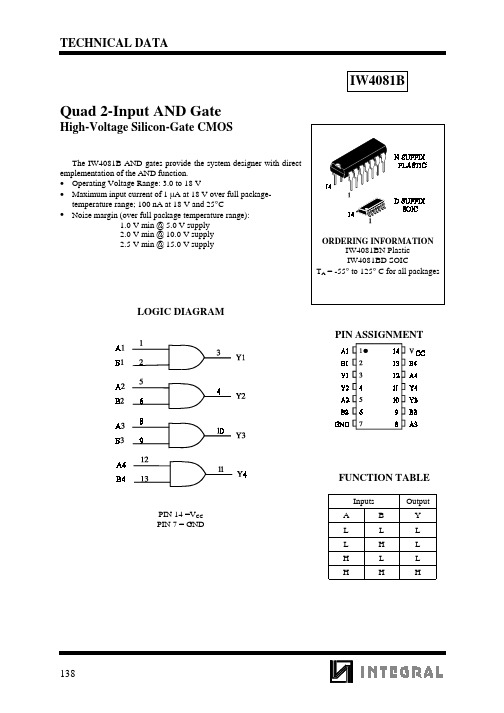
TECHNICAL DATA138Quad 2-Input AND GateHigh-Voltage Silicon-Gate CMOSThe IW4081B AND gates provide the system designer with direct emplementation of the AND function.• Operating Voltage Range: 3.0 to 18 V• Maximum input current of 1 µA at 18 V over full package-temperature range; 100 nA at 18 V and 25°C• Noise margin (over full package temperature range):********************************************************IW4081BLOGIC DIAGRAMPIN 14 =V CC PIN 7 = GNDPIN ASSIGNMENTFUNCTION TABLEInputsOutput A B Y L L L L H L H L L HHHIW4081B139MAXIMUM RATINGS *Symbol ParameterValue Unit V CC DC Supply Voltage (Referenced to GND)-0.5 to +20V V IN DC Input Voltage (Referenced to GND)-0.5 to V CC +0.5V V OUT DC Output Voltage (Referenced to GND)-0.5 to V CC +0.5V I IN DC Input Current, per Pin±10mA P D Power Dissipation in Still Air, Plastic DIP+ SOIC Package+750500mW P D Power Dissipation per Output Transistor 100mW Tstg Storage Temperature-65 to +150°C T LLead Temperature, 1 mm from Case for 10 Seconds (Plastic DIP or SOIC Package)260°C*Maximum Ratings are those values beyond which damage to the device may occur.Functional operation should be restricted to the Recommended Operating Conditions.+Derating - Plastic DIP: - 10 mW/°C from 65° to 125°CSOIC Package: : - 7 mW/°C from 65° to 125°CRECOMMENDED OPERATING CONDITIONSSymbol ParameterMin Max Unit V CC DC Supply Voltage (Referenced to GND)3.018V V IN , V OUTDC Input Voltage, Output Voltage (Referenced to GND)0V CC V T AOperating Temperature, All Package Types-55+125°CThis device contains protection circuitry to guard against damage due to high static voltages or electricfields. However, precautions must be taken to avoid applications of any voltage higher than maximum rated voltages to this high-impedance circuit. For proper operation, V IN and V OUT should be constrained to the range GND ≤(V IN or V OUT )≤V CC .Unused inputs must always be tied to an appropriate logic voltage level (e.g., either GND or V CC ).Unused outputs must be left open.IW4081B140DC ELECTRICAL CHARACTERISTICS (Voltages Referenced to GND)V CCGuaranteed Limit Symbol Parameter Test Conditions V ≥-55°C 25°C ≤125°C Unit V IHMinimum High-Level Input VoltageV OUT =0.5V or V CC - 0.5V V OUT =1.0V or V CC - 1.0V V OUT =1.5V or V CC - 1.5V5.01015 3.5711 3.5711 3.5711VV ILMaximum Low -Level Input Voltage V OUT =0.5V V OUT =1.0VV OUT =1.5V 5.01015 1.534 1.534 1.534VV OH Minimum High-Level Output Voltage V IN =V CC5.01015 4.959.9514.95 4.959.9514.95 4.959.9514.95VV OL Maximum Low-Level Output Voltage V IN =GND or V CC 5.010150.050.050.050.050.050.050.050.050.05VI IN Maximum Input Leakage Current V IN = GND or V CC 18±0.1±0.1±1.0µA I CCMaximum Quiescent Supply Current (per Package)V IN = GND or V CC5.01015200.250.51.05.00.250.51.05.07.51530150µAI OLMinimum Output Low (Sink) Current V IN = GND or V CC U OL =0.4 VU OL =0.5 V U OL =1.5 V 5.010150.641.64.20.511.33.40.360.92.4mAI OHMinimum Output High (Source) Current V IN = GND or V CC U OH =2.5 VU OH =4.6 V U OH =9.5 V U OH =13.5 V5.05.01015-2.0-0.64-1.6-4.2-1.6-0.51-1.3-3.4-1.15-0.36-0.9-2.4mAIW4081B141AC ELECTRICAL CHARACTERISTICS (C L =50pF, R L =200k Ω, Input t r =t f =20 ns)V CCGuaranteed Limit Symbol ParameterV ≥-55°C25°C ≤125°C Unit t PLH , t PHLMaximum Propagation Delay, Input A or B to Output Y (Figure 1)5.010152501209025012090500240180nst TLH , t THL Maximum Output Transition Time, Any Output (Figure 1)5.010152001008020010080400200160nsC IN Maximum Input Capacitance-7.5pFFigure 1. Switching WaveformsEXPANDED LOGIC DIAGRAM(1/4 of the Device)。
SecuriTEST IP接口数据表.pdf_1693854590.8454423说明书
Datasheet for SecuriTEST IPInterfacesEthernet port:o Ethernet 100Base-T - LAN/Network/Camera/RJ45 TDR test (1000Base-T)RJ45 port:o PoE IN - Pass-through PoE to the Ethernet port only no data pass through.o Cable test - Cable test only Not Ethernet, no network connection.Wi-Fi:o Built in Wi-Fi 802.11b/g/n (2.4GHz only) up to speed 150Mb/s client to access the network for testing. Coax port:o BNC (f) video IN/HD Coax IN – Analogue, TVI, CVI, AHD inputo BNC (f) video out – Analogue video bar outputRS485 port: RS485 male “Phoenix” type connector for PTZ control and communications testHDMI port:o HDMI IN:o HDMI supports: 720×480p /720×576p /1280×720p /1920×1080p /1024×768p/1280×1024p /1280×900p /1440×900p video formats.o Does not support HDCP copy protected video sourceso HDMI OUT: 1 channel HDMI output1280x720p, 1920x1080p user selectable.Audio port:o Audio IN: 3.5mm female socket for audio line ino Audio Out: 3.5mm female socket for audio line outDC output: 4.0x1.7mm female socket for 12V/2A DC output (centre positive polarity)USB port: Type A USB on 5V/2A DC power output only (No data transfer)SD card slot: MicroSD card readerDC input: 12V DC charge port with 5.5x2.1mm socket. Tester can operate and charge battery simultaneously. LED IndicationBattery:o ON - charging,o OFF - fully charged when charge is ON oro OFF – no charging when charge is OFFo Flash – no battery fitted (charge LED is ON)Charge: DC 12V IN is ONTx & Rx:Flash - Tx & Rx data for RS485ON – Standby (both Tx & Rx ON)Test functionsIP Camera Test:o Max video input resolution: 4K (8MP).o Codec support: MJPEG, MPEG4, H.264, H.265 (mainstream)o ONVIF support: relevant part of profile S,Q,Go IP address discovery & assign: auto discover static IP address of direct-connected camera or assign IP address to the camera with dynamic IP address setting ( from internal DHCP server) automatically.o Stream support: RTSP (Real Time Streaming Protocol)o Non ONVIF and proprietary IP camera support: manual IP address, port and model selection for non ONVIF supported cameras brand including ACTi, AIPU, APD, Axis, Aebell, Arecont Vision, BILL, BM,Bestecher, Bosch, CityTech, CYZ, Changying, Colin, Costar, Dahua , DOZENY, DVO, DVSONE, Devele,Etrovision, FOKO, FORSECU, FS, Finetida, GOLBONG, GREAT, Geovision, Grandeye, HI-SHARP, Hikvision, HISIDE, HZWS, HanbangGaoKe, HawKeye, Hitron, Honewell, HuiSun, hongben, ISEC, Infinova, JETVIEW,JOOAN, JOVISION, JUAN, Jbvideo, JieGao, JingShiKang, KEDACOM, KINPUS, KeJun, KumKang, LEFOUND, LILIN, LanDunSiAn, Longse, MaxxOne, NJBESTWAY, Neitway, OSKA, PN3D, Panasonic, Pelco, PengRunDa, Pinshi, QIDUN, Samsung, SANTACHI, SHIKO,SONY, STJIATU, STYCO, Safer, SecurityTronix, Seeyou,SongXin, Sunell, SuperSight, TBTEC, TIANDY, TP-LINK, TVT, TianLong, TruVue, Uniview,VIDIACNET,VIVOTEK, VSTON,VVS-CCTV, VideoNet, Vista, WAPA, WATCHMAN, WEISKY, Woshida,XiangWei, XinLong, YH, YIDUN, YJX, YSJ, YXAF, YueTian, YunShiAn, ZKTeco, ZLD …o PTZ, focus, aperture: Key pad and screen gesture to control of aperture, zoom, focus, pan, tilt.o Digital zoom: Up to 20 times (subject to camera availability)o Rapid video: One key discovery of active network cameras and access to camera setup and programming via ONVIF.Web browser: ChromeAnalogue (CVBS) camera test:o Video input: 1 channel analogue CVBS signal PAL & NTSC auto detectiono Video level meter: Peak video signal level, Sync signal level, Colour, Chroma level measuremento Video output: colour bar, blue or black full screen in NTSC or PAL formats.o Dual window display: CVBS floating on screen and IP camera test results at the same time for analogue and IP converter test monitoro PTZ control: Supports RS485 control, Baud 600-115200bps, Compatible with more than 30 protocols such as PELCO-D/P, Samsung, Panasonic, Bosch etc. (detail see HD Coax PTZ part) o PTZ address scan: auto detect camera’s PTZ addresso PTZ data monitoring: Captures and analyses the command data from PTZ controller. Manual transmit of hexadecimal codes in RS485 for PTZ control testing.HD Coax (TVI, CVI, AHD) camera test:o TVI: 8MP (4K) 3840 x 2160 15 fps, 5MP 2592 x 1944P 12.5/20 fps, 4MP 2688 x 1520P 15fps; 2560 x 1440P 15/25/30 fps, 3MP 2048 x 1536P 18/25/30 fps, 2MP (1080P) 1920 x 1080P 25/30 fps, 720P 1280 x 720P25/30/50/60 fps, UTC control/ call OSD menuo CVI: 8MP (4K) 3840 x 2160 12.5/15 fps, 4MP 2560x1440P 25F/30 fps, 1080p 1920 x 1080P 25/30 fps, 720p 1280 x 720P 25/30/50/60fps, UTC control d call OSD menuo AHD: 5MP 2592 x 1944P 12.5/20 fps,4MP 2560x1440P 15/25/30 fps, 3MP 2048x1536P 18/25/30 fps, 1080p 1920x1080P 25/30fps,720P 1280x720P 25/30 fps ,UTC control d call OSD menuo Images: Snapshot/view, video record/play, screenshoto PTZ control:Port type - UTC Coaxitron®:▪PTZ - Address, pan speed, tilt speed, set & recall position▪Menu - arrows control with address•Port type - RS485:▪Protocol: ALEC, AD168(M-B), Bosch OSRD, CBC, DAT-SD, DH-YTC06, Fastrax, HD600, Hikvision, Kalatel ASC, LC-NEW, LG-MULTIX, Lilin-FAST, Lilin-MLP2, Minking A01, MinkingB01, Molynx, Panasonic, Pelco D, Pelco P, Samsung, Samsung SPD, SIEMENS, SONY-EVI,Santachi, TeleEye DM2, Vcltp, Vicon, WV-CS850, YAAN, YAAN-0, YAAN-1▪Baud rate: 150, 300, 600,1200,2400,4800,9600,19200, 38400,115200▪Address, Pand & Tilt speed, Position set & Recallo Zoom: Key pad control manual & digital (5x max)Power output:o PoE: DC48V PoE/PoE+, 24W maxo DC 12V: DC12V/2A power for IP & analogue cameraso DC 5V: DC5V 2A power output via USB to charge portable devicesPoE & Voltage testo PoE IN: voltage, power and pins usedo LAN/Network: voltage, power and pin usedo12V DC IN: voltage, power consumed (operating and charging power consumption)o12V DC OUT: voltage, power consumed by attached deviceo PoE link check: PD (Powered Device) port on cable Tracer/Remote Test’s PoE status of link and pairs used with LED indicators for 12,36 or 45,78 pins.Ethernet cable test:o Twisted-pair test: Reports: – straight, crossed-pair, open, short and cross-over (MDI-MDIX) with Tracer/Remote.o RJ45 TDR test: Length 180m (max), Resolution +/-1m; estimated attenuation (dB/100m or dB/100feet) with good, poor and bad colour status; reflection %; impedance (Ω); delay skew (when connected to1000Mb/s network device only), pin number with pair length. Continuous and single test mode.o Digita l Tone generator: 4 different tone selections for cable tracing.o Cable trace: Trace and locate cables with the included Tracer/Remote. Digital tone technology eliminates electrical noise/hum associated with traditional analogue tracing probes. Eight (8) volume levels,headphone jack for use in noisy environments, non-conductive tip to prevent short circuits and integrated LED flashlight. Requires 2 x 1.5V AAA (LR03) batteries (not included).IP Network test:o Traffic monitoring: real-time upstream/downstream bandwidth histogram, tester IP address and link speed and full/half-duplex condition.o Ping: Local & destination IP address, packet size, number of ping tests and inter-packet delay.o IP Scan: Scan for active devices within selected IP address range (subnet). Scan selected IP address for available TCP/UDP port services.o Port flash: Flash the link LED on of the switch to visually identify the port to which SecuriTEST IP is connected.o DHCP Server: Fully configurable DHCP server to allow dynamically configured devices to operate when a network router is not installed. Start/stop IP address range, lease time, connected client list display.o Trace Route: Display IP address and delay time of up to 30 hops (routers) between device and target URL/IP address.o Available IP: Create list of IP addresses and to scan for availability checking. Tester will scan each address and identify if the address is available or in use by a network device. Use to find available IP addressedwhen before configuring a new device with a static address.o Network IP Scan: Cross-subnet IP scan on any linked network. Lists IP address of devices on multiple subnets compared to IP Scan function which only lists devices on the same subnet as the tester.Media playback/record applications:o Video: RTSP player, Video player, VLCo Audio: Audio recorder, Audio playerImage capture:o Capture still image from connected camera (can be attached to test reports).o Record video stream from connected camera.o Capture current tester screen.Audio:o Audio IN: 1 channel audio signal input from camera to record, listen and play via media player or audio recorder/player; 2.5 mm (1/8”) connector.o Audio OUT: 1 channel audio signal output to monitor audio from cameras with microphone; 2.5 mm (1/8”) connector.o Speaker: Internal two speakers for system indicators and audio playback from cameras or other media files.Test report (ONVIF only): PDF format witho Company/customer project details,o Tester information,•Serial number/hardware version/firmware version/software version•Date/time seto Date/time of test conductedo Camera manufacturer/model/name/software version/Date & timeo Camera network configuration,o Link speed and duplexo IP/gateway/DNS/MAC addresses, subnet masko Dynamic/static configurationo Video stream information,o Video resolutiono Frame rateo Bit rateo Encoding (CODEC) typeo Attach up to six (6) video still snapshot images,o Operator’s noteso Attach company/customer logoQuick Access Shortcut menu: Single button access to eight (8) user-selectable functionsRemote view: View tester screen on other network device using RTSP (Real Time Streaming Protocol).Results & upgradeJOBS: Shortcut to user storage area with folders for Audio/ Logos/ Photos/ Reports/ Screenshots/ Videos. Single button copy all files/directories from internal JOBS folder to external SD card.File management:o File explorer: copy, save, delete, cut, paste, transfer to internal and external SD cardo FTP: results to be accessed and managed via FTP with tester configured as a server or client.o MicroSD card: transfer results to other devices or install software updates.Upgrade: Auto & manual updates from microSD card.HelpVideo introduction: a quick video clip for basic operation introductionUser guide: Context sensitive on-line helpQuick reference guide: a quick reference guide for starting to operate the testerFAQ: a list of commonly asked questions regarding to tester operation.GeneralDisplay:o Screen: 7 inch capacitive touch screen with 1920x1200 resolution (324 ppi).o Screen locking: user password setting for secured tester access.o Screen rotation: rotating screen for ceiling camera adjustment before mounting.o Sleep timer: 1-30 min, disengage.Storage: 10GB internal SD card, 8GB external microSD card included (supports up to 16 GB).Date & Time: Date,Time & time zone selection, 24 hours format, manual and auto sync.Power: Charger: input 110-240VAC, 50/60Hz, 0.6A; output 12VDC, 2A, centre pin positive polarity; US, UK, EU, Australia AC plug adapters.Battery:o Capacity: Field user exchangeable 7.4V Lithium polymer battery, 5000mAh, 37Who Operation time: 10 hour (typical) continuous operation without external PoE/DC12V load; 4.5hours (typical) with 3.5 watt PoE camera load.o Charge time: < 8 hours from empty.Language: English, French, German, Spanish, Italian, Portuguese, ChineseLength units: meter, feetOperating Temperature: -10℃---+50℃Operating Humidity: 30%-90%Dimension 252 mm x 160 mm x 48 mm/ 10.0 in x 6.3 in x 1.9 in (approximate)Weight: 1.0 Kg/2.2 lbs (including battery)Standard complianceCE RED directive:•EN 60950-1:2006+A11:2009+A1:2010+A12:2011+A2:2013•EN 301 489-1 V1.9.2 (2011-09)•EN 301 489-17 V2.2.1 (2012-09)•EN 300 328 V1.9.1 (2015-02)•EN 62479:2010FCC:•FCC Part 15 Subpart BRoHS:•EN62321:2012•EN 14372:2004•EPA 3540:1996Tone Tracer/Remote CE directive:•EN55032:2015•EN61000-3-2:2014•EN61000-3-3:2013•EN55024:2010+A1:2015IDEAL INDUSTRIES NETWORKS DIVISIONUnit 3, Europa Court, Europa Boulevard, Warrington, Cheshire, WA5 7TN, UK. Tel. +44 (0)1925 444 446 | Fax. +44 (0)1925 445501******************** | Specification subject to change without notice. Errors & Omissions Excepted © IDEAL Networks 2018Publication No.: 171870A subsidiary ofIDEAL INDUSTRIES INC.。
HIP0082资料
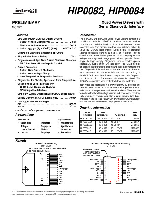
元器件交易网
HIP0082, HIP0084
Absolute Maximum Ratings TA = 25oC
Supply Voltage (Logic and Control), VCC . . . . . . . . . . . . -0.3V to 7V Power MOSFET Drain Voltage, VO (Note 3) . . . . . . -0.7 to VCLAMP Output Clamp Energy, EOK (See Note 5). . . . . . . . . . . . . . . . . 70mJ Input Voltage (Logic and Driver Inputs), VIN. . . .-0.5V to VCC +0.5V Maximum Output Current, Outputs 1 and 2 . . . . . . . . . . . . . . . . +2A Maximum Output Current, Outputs 3 and 4 . . . . . . . . . . . . . . . . +5A Maximum Total Output Current, All Outputs ON. . . . . . . . . . . . . +8A Maximum Peak Output Current, IO(MAX), (Note 4) . . . . . -5A to ISC
15
IN3
14
OUT3
13
IN1
12
OUT1
11
R/W
10
VCC
9
RST
8
GND (VSS)
HillStone最新配置手册之欧阳地创编
HillStone SA-2001配置手册1网络端口配置22防火墙设置123VPN配置144流量控制的配置244.1P2P限流244.2禁止P2P流量254.3IP流量控制284.4时间的设置294.5统计功能325基础配置35本文是基于安全网关操作系统为Version 3.5进行编写,如版本不同,配置过程有可能不一样。
1 网络端口配置SA-2001安全网关前面板有5个千兆电口、1个配置口、1个CLR按键、1个USB接口以及状态指示灯。
下图为SA-2001的前面板示意图:将网线接入到E0/0。
防火墙的ethernet0/0接口配有默认IP地址192.168.1.1/24,但该端口没有设置为DHCP服务器为客户端提供IP地址,因此需要将PC机的IP地址设置为同一网段,例如192.168.1.2/24才能连上防火墙。
通过IE打开192.168.1.1,然后输入默认的用户名和密码(均为hillstone)登录后的首页面。
可以看到CPU、内存、会话等使用情况。
很多品牌的防火墙或者路由器等,在默认情况下内网端口都是划分好并且形成一个小型交换机的,但是hillstone的产品却需要自己手工设置。
在本文档中,我们准备将E0/0划分为UNTRUST口连接互联网,E0/1~E0/4总共4个端口我们则划到一个交换机中并作为TRUST口连接内网。
在网络-接口界面中,新建一个bgroup端口,该端口是一个虚拟的端口。
因为bgroup1接口需要提供路由功能,因此需要划入到三层安全域(trust)中。
输入由集团信息中心提供的IP地址。
在管理设置中,尽量将各个管理功能的协议打开,尤其是HTTP功能。
建好bgroup1之后,对网络-接口页面中的e0/1~e0/4分别修改,依次将它们划归为bgroup1。
设置好交换机功能后,还需要设置DHCP功能,以便PC机接入时可以自动获取IP地址。
新建一个DHCP地址池根据集团信息中心提供的IP地址段设置IP地址池。
Fujitsu PSWITCH 2048 数据表 数据中心以太网连接的强大、经济高效的开关说明书
Data SheetFujitsu PSWITCH 2048Powerful, cost-efficient switch for data center EthernetconnectivityData centers continue to evolve, creating a need for an infrastructure that can support growth in virtual machines, distributed applications, data, as well as the transition to public and private cloud environments without compromising performance. Today’s networks need to support the flexible connectivity of any device from any place in a secure manner. They have to provide an automated quality of service management when assigning bandwidth to the various usage scenarios as this cannot be done fast enough on a manual basis.Fujitsu has developed a suite of top-of-rack switches that support flexible and efficient scale-out server infrastructures, especially in combination with new modular servers. This approach results in several improvements, including infrastructure efficiency for cloud computing, end-to-end virtualization andconsolidation. Close partnerships with network technology partners complement the portfolio for building complete IT infrastructures. A lot of new use cases are based on Ethernet networks, with high bandwidths and increasingly virtualized fabric architectures for building dynamic data centers. And it goes without saying that Fujitsu server and storage systems are fully compatible with our own products as well as products from our partners.PSWITCH 2048The FUJITSU PSWITCH 2048 delivers innovative technology to enhance and simplify networks. It is a 1U low-latency, Layer 2/3, Ethernet switch and provides a rich set of advanced networking features, making the PSWITCH 2048 an ideal platform for traditional Top-of-Rack (ToR) switch deployments. With support for forty-eight 10GbE BASE-T (PSWITCH 2048T) or SFP+ ports (PSWITCH 2048P) as well as six 40GbE QSFP+ ports, these switch provide the efficiency and flexibility you need to support cloud computing, virtualization and consolidation. For organizations seeking automated provisioning capabilities to improve IT agility, the PSWITCH 2048 accelerate time to production through automatic discovery of network devices. This reduces the initial efforts, ongoing maintenance time and costs. The switch is designed for the next-generation data centers with advanced features such as Data Center Bridging (DCB), Edge Virtual Bridging (EVB) and VXLAN Tunnel End Point (VTEP) to support large-scale virtualization and software-defined Networking. In order to adapt to the individual situation as best as possible, the switch can be used in various switch modes. Beside the default Layer2 switching support it provides the possibility of the end host mode (EHM) to simplify the port settings for connecting to a network in operation. This functionality can be beneficial in blade transition projects.Despite all these features, the switch offers a cost-effective solution because there are no additional license costs for the number of used ports. The PSWITCH 2048 is ideally suited for a variety of different solutions such as hyper-convergedinfrastructures, e.g. VMware VSAN , Storage Spaces Direct (S2D) scenarios or also as dedicated storage network.Features & BenefitsTechnical detailsPSWITCH 2048Connection type Ethernet ToR Switch10/40 Gbit/s Ethernet Switch, Layer2 switching support / Layer3 Service support, End Host Mode (EHM)InterfacesDown-link ports48 x 10 Gbit/s Eth (SFP+ / RJ45)Up-link ports 6 x 40 Gbit/s Eth (QSFP+)Management ports 1 x RJ45 Serial Port 1 x 10/100/1000Mbps LAN PortOrder code Application Type / mode Connector / cable LengthS26361-F3989-E600Ethernet 10 Gbit/s SFP+ Twinax Cable / active SFP+ / 2m or 5mS26361-F3989-L102Ethernet 10 Gbit/s SFP+ Twinax Cable / active SFP+ / 2mS26361-F3989-L105Ethernet 10 Gbit/s SFP+ Twinax Cable / active SFP+ / 5mS26361-F3989-L110Ethernet 10 Gbit/s SFP+ Twinax Cable / active SFP+ / 10mS26361-F3873-E500Ethernet 10 Gbit/s SFP+ Twinax Cable / active SFP+ / 3m or 5mS26361-F3986-E400Ethernet 40 Gbit/s QSFP+ Twinax Cable / passive QSFP+ / 2m or 5mTechnical specificationsLayer 2 feature Virtual LAN(IEEE802.1Q)Link Aggregation(LAG)Spanning Tree ProtocolLoop detectionLink Down RelayRemote Switch Port Analyzer(RSPAN)Unidirection Link Detection(UDLD)End Host Mode (EHM)Layer 3 feature IPv4 - ARP / ICMP / IRDPIPv6 - NDPRoutingRouting Information Protocol (RIP / RIPng)Open Shortest Path First (OSPF)Boarder Gateway Protocol 4 (BGP4)Virtual Router Redundancy Protocol (VRRP)Equal Cost Multi-Path (ECMP)UDP Relay / IP HelperDNS Client and DNS RelayLink-Local Multicast Name Resolution (LLMNR)Virtual Routing and Forwarding (VRF)Link aggregation Static LAGIEEE 802.1ax-2008 standard (LACP)support up to 48 ports in a LAGvirtual port channels (VPCs)Spanning tree Spanning Tree Protocol (STP)Rapid Spanning Tree Protocol (RSTP)Multiple Spanning Tree Protocol (MSTP)DCB features Priority Flow Control (PFC)Enhanced Transmission Selection (ETS)Congestion Notification (CN)Data Center Bridging Extensions (DCBX)Technical specificationsNetwork protocol and standards compatibility IEEE 802.1ab LLDPIEEE 802.1p Class of ServiceIEEE 802.1d Spanning Tree ProtocolIEEE 802.1Qau Congestion NotificationIEEE 802.1Qaz Enhanced Transmission Selection (ETS)IEEE 802.1Qbb Priority Flow Control (PFC)IEEE 802.1q VLANIEEE 802.1s Multiple Spanning Tree ProtocolIEEE 802.1w Rapid Spanning Tree ProtocolIEEE 802.1x Port Based Network Access ControlIEEE 802.1ax-2008 Link AggregationIEEE 802.3x Flow ControlIEEE DCBX Data Center Bridging Exchange protocol proposal for 802.1 Qaz IPv4, IPv6 and mixed IPv4/IPv6 network protocolsPerformance720Gbps switching bandwidth (1440Gbps duplex)Automatic address learning function to build the packet-forwarding information table. The table contains up to 96KMAC addresses12 MB of packet buffer memorySupport Jumbo Frame up to 9KbyteStore-Forward mode - Cut-through is available to minimize the latencIP multicast features IGMP SnoopingMLD SnoopingSnooping QuerierMulticast Static Routes (MRoutes)Internet Group Management Protocol (IGMP) v2/v3Mluticast Listerner Discovery (MLD) v1/v2Distance Vector Multicast Routing Protocol (DVMRP)Protocol Independent Multicast - Dense Mode (PIM-DM)Protocol Independent Multicast - Sparse Mode (PIM-SM)VLAN Port Based VLANMAC Based VLANProtocol Based VLANIP Subnet Based VLANPrivate VLANManagement Telnet/SSHNetwork Configuration Protocol(NETCONF)Simple Network Management Protocol(SNMP)Remote Monitoring(RMON)Open vSwitch Database(OVSDB) management protocolDimensions / WeightDimensions (W x D x H)440 x 460 x 44 mmWeight8.4 kgEnvironmental complianceOperating ambient temperature0 - 40 °COperating relative humidity10 - 90 % (relative humidity)ProductEurope CEUSA/Canada FCC Class AUL/CSAGlobal CBRoHSJapan VCCIJATERussia EACSouth Korea KCChina CCCAustralia/New Zealand AS / NZS CISPR 22Taiwan BSMISaudi Arabia SASOCompliance link https:///sites/certificatesCONTACTFUJITSU LIMITEDMies-van-der-Rohe-Straße 880807 München GermanyWebsite: 2023-08-02 INT-ENworldwide project for reducing burdens on the environment.Using our global know-how, we aim to contribute to the creation of a sustainable environment for future generations through IT.Please find further information at http://www./global/about/environmenttechnical specification with the maximum selection of components for the named system and not the detailed scope ofdelivery. The scope of delivery is defined by the selection of components at the time of ordering. The product was developed for normal business use.Technical data is subject to modification and delivery subject to availability. Any liability that the data and illustrations are complete, actual or correct is excluded. Designations may be trademarks and/or copyrights of the respective owner, the use of which by third parties for their own purposes may infringe the rights of such owner.More informationAll rights reserved, including intellectual property rights. Designations may be trademarks and/or copyrights of therespective owner, the use of which by third parties for their own purposes may infringe the rights of such owner. For further information see /emeia/resources/navigation/terms-of-use.html Copyright 2020 FUJITSU LIMITED。
HIPERFACE协议说明书(中文版)
缺点是这些编码器系统不仅自身成本较高,三个系统的安装及布线都会产生较高成本,同时组件数量 过多也意味着发生故障的可能性提高。
应用紧凑型低功率控制器的并考虑以下几个方面,可潜在地降低成本: • 具有霍尔传感器的换向编码器设计。 • 如无必要,可省去最终定位器。 • 使用“无传感器控制”软件来代替测速发电机。
因此,两个不同的位置数据片的重叠数位始终采用相同的价位,从而形成位置值差异。如果两个位置 值指向不同的周期,则具有较低分辨率的位置值将向较小差异的方向调整 ± 1 周期。
图6
正交_计数器 模拟_角度
多圈
12 位圈
高分辨率绝对位置、 12 位圈
单圈(周期)
周期/圈
周期/圈
同步
正交_计数器:分辨率为 4* 周期数的控制器内位置值。 模拟_角度:一个周期内的模拟信号所计算的角度 绝对_位置:从参数通道读取的绝对位置
电源电压 乍看之下,在控制器内生成额外的、不寻常的 8 V 电压似乎是一个该系统的缺陷,但是这一点能够
确保向 HIPERFACE® 电机反馈系统提供充足的电源电压(即使驱动器和电机反馈系统之间的距离较长)。 这样就无需使用额外的电源(例如带电压反馈电缆的电源)。
RS485 接口 RS485 接口毫无疑问可称为行业标准。该物理接口需要一个 130 Ω 的终端电阻、两个偏压电阻器及
绝对型编码器始终可传输完整的位置数据,因此非常适用于位置控制应用。位置数据的数字传输需要 电缆具备较高的传输带宽,并且仅在一定条件下才可实时启用。此外,由于传统的绝对型编码器需要投入 大量劳动,所以相对较贵。传统型可读取位于玻璃盘上的二进制数据代码,因此需要对每个二进制数字进 行相应的光学扫描,所有的扫描都必须进行调整,以避免发生读取错误。
SHR-4081P-chn-2

SHR-4081P
-
10-23
G
G
G
10-24
G
SHR-4081P
G
G
G
1
2
3
4
!
10-25
©
©
©
@
“
” “ “ ” © © © “ “ ” © © ” © © ” ©
10-26
#
$
G
2 5 8 7 3 6
1 4 9
! @ # $ % ^ & * (
10-27
G
SHR-4081P
2 1 3
4
! @ # $ % ^ &
SHR-4081P
SHR-4081P
10-44
G
!
SHR-4081P
@
4081N/P
SHR-4081P
#
SHR-4081P
G
!
4081N/P
10-45
G
-
SHR-4081P 5 30
G
OSD
G
G
SHR-4081P SHR-4081P
G
-
10-46
SHR-4081P SHR-4081P
3
1
2
!@ #
45
1
2
3
4
10-20
!
a a
b b c c
!
@ # $
@#$
@ @ #
# $ @
$
#
$
10-21
G
1
!
1 2 3
! @ #
10-22
8
G
SHR-4081P
1
3 2
- 1、下载文档前请自行甄别文档内容的完整性,平台不提供额外的编辑、内容补充、找答案等附加服务。
- 2、"仅部分预览"的文档,不可在线预览部分如存在完整性等问题,可反馈申请退款(可完整预览的文档不适用该条件!)。
- 3、如文档侵犯您的权益,请联系客服反馈,我们会尽快为您处理(人工客服工作时间:9:00-18:30)。
-
µA
6.8 7.6 8.25 6.5 8.5
V
6.5 7.1 7.8 6.25 8.1
V
0.17 0.4 0.75 0.15 0.90
V
AHB, BHB Undervoltage Threshold INPUT PINS: ALI, BLI, AHI, BHI, & DIS
VHBUV
Referenced to AHS & BHS
VDD Falling Undervoltage Threshold
欠压滞后
IDD
IDDO
IAHBL , BHBL
I
IAHBH , BHBH
I
IAHBO , BHBO
I
I
HLK
V DDUV+ V DDUVUVHYS
All inputs = 0V, R DEL = 100K
All inputs = 0V, R
2注0:V/所ns有的电压都是相对V
SS 除非另有规定.
热阻
SOIC封装. . . . . . . . . . . . . . . . . . . . . . . . . .D.IP. .封装. . . . . . . . . . . . . . . . . . . . . . . . . 最大. .功. .率. 耗散. . . . . . . . . . . . . . . . . . . . . . . .见 曲存线储温度范围. . . . . . . . . . . . . . . . . .-65°C至 +操1作50最°C大.结温. . . . . . . . . . . . . . . . . . +焊1接50温°C度(10秒). . . . . . . . . . . . . . . . . . . . +3(00对°C于SOIC - 铅针头))
5
6.0
7
4.5 7.5
V
低电平输入电压 高电平输入电压 输入电压迟滞 低电平输入电流 高电平输入电流 TURN-ON DELAY PIN DEL
V IL
Full Operating Conditions
V IH
Full Operating Conditions
IIL
VIN = 0V, Full Operating
工作条件
电源电压,V
DD . . . . . . . . . . . . . . . . . . . . . . . . . +8.5 V到
对V电压
SS . . . . . .+.1.5. .V. . . . . . . . . . . . . . . . . . . . -1.0V至
电压AHB,BHB. . .+.1..0. .V.
VDD 静态电流
VDD 工作电流
AHB, BHB Off Quiescent Current AHB, BHB On Quiescent Current AHB, BHB Operating Current AHS, BHS Leakage Current
VDD Rising Undervoltage Threshold
®
数据表
2006年1月3日
HIP4082
FN3676.4
80V,1.25A峰值电流H桥 FET驱动器
HIP4082是一个中频,中压 H桥N沟道MOSFET驱动IC,在16引脚塑料SOIC(N)和DIP封装.
专门针对PWM控制电机和UPS应用,桥梁基础的设计变得简单 ,灵活与HIP4082 H桥驱动器.与运行在高达80V,器件最适合 于中等功率水平的应用.
1.2 2.3 3.5 0.85 4
mA
2.2 4.0 5.5 1.9 6.0
mA
1.5 2.6 4.0 1.1 4.2
mA
2.5 4.0 6.4 2.1 6.6
mA
0.5 1.0 1.5 0.4 1.6
mA
65 145 240 40 250
µA
.65 1.1 1.8 .45 2.0
mA
-
-
1.0
-
引脚
HIP4082 (PDIP,SOIC)
顶视图
BHB 1
BHI 2
BLI 3
ALI 4
DEL 5
V
6
AHI 7
DIS 8
16 BHO 15 BHS 14 BLO 13 ALO 12 V 11 AHS 10 AHO 9 AHB
1
CAUTION: These devices are sensitive to electrostatic discharge; follow proper IC Handling Procedures.
IIH
VIN C= o5nVd,itFiounllsOperating
Conditions
-
-
1.0
-
0.8
V
2.5
-
-
2.7
V
-
35
-
-
-
mV
-145 -100 -60 -150 -50
µA
-1
-
+1 -10 +10
µA
死区时间
T DEAD
R DEL = 100K R DEL =
10K
2.5 4.5 8.0 2.0 8.5
DD +0.3V
1电5压0°ACH)S,BHS. . . . . -6V(瞬态)至70V(-55°C至
1电5压0°ACH)B,BHB. . . . . . . .
AHS, BHS -0.3V到V AHS, BHS +V DD
V电压ALO,BLO. . . . . . . . . . . . . . . . .
DRIVER
V
13 ALO
BLO 14
DRIVER
TURN-ON DELAY
2
FN3676.4
January 3, 2006
Typical Application (PWM Mode Switching)
HIP4082
12V PWM INPUT DELAY RESISTOR
DIS
1 BHB 2 BHI 3 BLI 4 ALI 5 DEL 6V 7 AHI 8 DIS
BHO 16
BHS 15
BLO 14
ALO 13
V
12V 12
AHS 11
AHO 10
AHB 9
FROM OPTIONAL OVERCURRENT
LATCH
GND R
TO OPTIONAL
+
CURRENT CONTROLLER OR
-
OVERCURRENT LATCH
80V LOAD
R GND
3
FN3676.4
device at these or any other conditions above those indicated in the operational sections of this specification is not implied.
θJA (°C / 1W1)5 90
电气规格
参数
相似的HIP4081,它有一个灵活的输入协议 驾驶每一个可能的开关组合除外 这将导致一个贯通的条件.该 HIP4082的降低驱动电流允许使用更小的包装,它有一个更广泛的 可编程死区时间(0.1〜4.5µs),使其成为理想的开关频率高达 200kHz.HIP4082不包含内部电荷泵,但不包括上部驱动电路的非闭锁电 平转换的翻译器.
V
12
DETECTOR UNDERVOLTAGE
ALI 4 DEL 5 BLI 3
V
6
U/V
LEVEL SHIFT
TURN-ON DELAY
DRIVER
9 AHB BHB 10 AHO BHO 16
1 DRIVER
11 AHS
BHS 15
LEVEL SHIFT
U/V
TURN-ON DELAY
TURN-ON DELAY
All other trademarks mentioned are the property of their respective owners.
应用框图
12V
BHO
BHS
BHI
BLO
BLI HIP4082
ALI
ALO
AHI
AHS
AHO
GND
HIP4082
80V LOAD
GND
功能框图
BHI 2 AHI 7 DIS 8
这组功能和规格进行了优化应用对尺寸和成本是重要的.对于需要 更高的驱动能力的HIP4080A和HIP4081A建议.
订购信息
PART 数
PART
TEMP.
标记范围(℃)
包装
HIP4082IB* HIP4082IB
HIP4082IBZ* 4(0注82)IBZ
-55到+125 16 Ld为 S-5O5到IC(+1N25)1M61L6d.1为5 SOIC(Ny 3, 2006
HIP4082
绝对最大额定值
热信息
电源电压,V
DD . . . . . . . . . . . . . . . . . . . . . . . . . . . -0.3V
逻辑I / O电压. . . . . . . . .至. .1.6.V. . . . . . . . . . 0电.3压VA到HVS,BHS. . . . . -6V(瞬态)至80V(25°C至
1-888-INTERSIL or 1-888-468-3774