M5M5V408BTP-85L中文资料
MAX485中文资料
{ UBRR1H=0; UBRR1L=103; UCSR1B=(1<<RXCIE1)|(1<<RXEN1)|(1<<TXEN1); //发送接收使能,使用中断方式, UCSR1C=(1<<UCSZ10)|(1<<UCSZ11); //0x06 8 位数据,1 位停止位,无校验
SIGNAL(SIG_UART1_RECV)//serial port 1 {
if(UCSR1A&(1<<RXC1)) {
rec1buff=UDR1; rec1_flag=1; } }
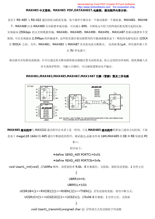
MAX481,MAX483,MAX485,MAX487,MAX1487 引脚(管脚)图及工作电路
MAX485 通讯程序与 MAX232 通讯程序在本质上是一样的,只是 MAX485 通讯程序需要加上通讯方向控制。下面 是基于 mega128 16AU 的 485 通信中断接收的程序,调试通过,晶振为外部 16M,MAX485 的 DE 和 RE 短接连 PC
Generated by Foxit PDF Creator © Foxit Software For evaluation only. MAX485 中文资料,MAX485 PDF,DATASHEET,电路图,通讯程序内容介绍: 是用于 RS-485 与 RS-422 通信的低功耗收发器,每个器件中都具有一个驱动器和一个接收器。MAX483、MAX48 7、MAX488 以及 MAX489 具有限摆率驱动器,可以减小 EMI,并降低由不恰当的终端匹配电缆引起的反射, 实现最高 250kbps 的无差错数据传输。MAX481、MAX485、MAX490、MAX491、MAX1487 的驱动器摆率不受 限制,可以实现最高 2.5Mbps 的传输速率。这些收发器在驱动器禁用的空载或满载状态下,吸取的电源电流在 120(A 至 500(A 之间。另外,MAX481、MAX483 与 MAX487 具有低电流关断模式, 仅消耗 0.1µA。所有器件都工作 在 5V 单电源下。 驱动器具有短路电流限制,并可以通过热关断电路将驱动器输出置为高阻状态,防止过度的功率损耗。接收器输入具 有失效保护特性,当输入开路时,可以确保逻辑高电平输出。
M80C85资料
GENRAL DESCRIPTIONThe MSM80C85AH is a complete 8-bit parallel; central processor implemented in silicon gate C-MOS technology and compatible with MSM80C85A.It is designed with higher processing speed (max.5 MHz) and lower power consumption compared with MSM80C85A and power down mode is provided, thereby offering a high level of system integration.The MSM80C85AH uses a multiplexed address/data bus. The address is split between the 8-bit address bus and the 8-bit data bus. The on-chip address latch : of a MSM81C55-5 memory product allows a direct interface with the MSM80C85AH.FEATURES•Power down mode (HALT-HOLD)•Low Power Dissipation: 50mW(Typ)•Single + 3 to + 6 V Power Supply•–40 to + 85°C, Operating Temperature •Compatible with MSM80C85A •0.8 m s instruction Cycle (V CC = 5V)•On-Chip Clock Generator (with External Crystal)•On-Chip System Controller; Advanced Cycle Status Information Available for Large System Control•Bug operation in MSM80C85AH is fixed•Four Vectored interrupt (One is non-maskable) Plus the 8080A-compatible interrupt.•Serial, In/Serial Out Port•Decimal, Binary and Double Precision Arithmetic •Addressing Capability to 64K Bytes of Memory •TTL Compatible•40-pin Plastic DIP(DIP40-P-600-2.54): (Product name: MSM80C85AHRS)•44-pin Plastic QFJ(QFJ44-P-S650-1.27): (Product name: MSM80C85AHJS)•44-pin Plastic QFP(QFP44-P-910-0.80-2K): (Product name: MSM80C85AHGS-2K)MSM80C85AHRS/GS/JS8-Bit CMOS MICROPROCESSORE2O0009-27-X2元器件交易网FUNCTIONAL BLOCK DIAGRAMINTR INTA 5.5 6.57.5TRAP SID SODRSTX1X2CLK OUT READY RD WR ALE S0S1IO / M HOLD HLDA RESET IN RESET OUT A15 - A8Address BusAD7- ADAddress/Data BusPIN CONFIGURATION (TOP VIEW)40 pin Plastic DIPA 8HOLD HLDA CLK(OUT)RESET IN READY IO/M S 1RD WR ALE S 0A 15A 14A 13A 12A 11A 10A 9V CC 39383736353433READY IO/M S 1RD WR NC ALE TRAP RST7.5RST6.5RST5.5INTR NC INTA 18192021222324A D 4N C A D 5A D 6A D 7G N D A 865432144S I DS O DR E S E T X 2X 1N C7891011121332313029S 0A 15A 14AD 0AD 1AD 2AD 314151617A 13V C C25262728A 9A 10A 11A 1243424140H O L D H L D AC L K (O R E S E T I NTRAP RST7.5RST6.5RST5.5INTR INTA AD 0A D 4A D 5A D 6A D 7G N D V C C A 8AD 1AD 2AD 3NC A 9A 10A 11N CMSM80C85AH FUNCTIONAL PIN DEFINITIONThe following describes the function of each pin:A 0 - A 7(Input/Output)3-state A 8 - A 15(Output, 3-state)Multiplexed Address/Data Bus: Lower 8-bits of the memory address (or I/O address) appear on the bus during the first clock cycle (T state) of a machine cycle. It then becomes the data bus during the second and third clock cycles.Address Bus: The most significant 8-bits of the memory address or the 8-bits of the I/O address, 3-stated during Hold and Halt modes and during RESET.Symbol FunctionALE (Output)Address Latch Enable: It occurs during the first clock state of a machine cycle and enables address to get latched into the on-chip latch peripherals. The falling edge of ALE is set to guarantee setup and hold times for the address information. The falling edge ALE can also be used to strobe the status information ALE is never 3-state.S 0 , S 1 , IO/M (Output)Machine cycle status:IO/M S 1 S 0 States S 1 can be used as an advanced R/W status. IO/M , S 0 and S 1 become valid at the beginning ofa machine cycle and remain stable throughout the cycle. The falling edge of ALE may be used to latch the state of these lines.RD(Output, 3-state)READ control: A low level on RD indicates the selected memory or I/O device is to be read thatthe Data Bus is available for the data transfer, 3-stated during Hold and Halt modes and during RESET.WR(Output, 3-state)WRITE control: A low level on WR indicates the data on the Data Bus is to be written into the selected memory or I/O location. Data is set up at the trailing edge of WR , 3-stated during Hold and Halt modes and during RESET.READY (Input)If READY is high during a read or write cycle, it indicates that the memory or peripheral is ready to send or receive data. If READY is low, the cpu will wait an integral number of clock cycles for READY to go high before completing the read or write cycle READY must conform to specified setup and hold times.HOLD (Input)HLDA (Output)HOLD ACKNOWLEDGE: Indicates that the cpu has received the HOLD request and that it will relinquish the bus in the next clock cycle. HLDA goes low after the Hold request is removed. The cpu takes the bus one half clock cycle after HLDA goes low.HOLD indicates that another master is requesting the use of the address and data buses.The cpu, upon receiving the hold request, will relinquish the use of the bus as soon as the completion of the current bus transfer. Internal processing can continue. The processor can regain the bus only after the HOLD is removed. When the HOLD is acknowledged, the Address, Data, RD , WR , and IO/M lines are 3-stated. And status of power down is controlled by HOLD.INTR (Output)INTERRUPT REQUEST: Is used as a general purpose interrupt. It is sampled on during the next to the last clock cycle of an instruction and during Hold and Halt states. If it is active, the Program Counter (PC) will be inhibited from incrementing and an INTA will be issued. During this cycle a RESTART or CALL instruction can be inserted to jump to the interrupt service routine. The INTR is enabled and disabled by software. It is disabled by Reset and immediately after an interrupt is accepted. Power down mode is reset by INTR.INTA (Output)INTERRUPT ACKNOWLEDGE: Is used instead of (and has the same timing as) RD during the instruction cycle after an INTR is accepted.RST 5.5RST 6.5RST 7.5(Input)RESTART INTERRUPTS: These three inputs have the same timing as INTR except they cause an internal RESTART to be automatically inserted.The priority of these interrupts is ordered as shown in Table 1. These interrupts have a higher priority than INTR. In addition, they may be individually masked out using the SIM instruction. Power down mode is reset by these interrupts.TRAP (Input)Trap interrupt is a nonmaskable RESTART interrupt. It is recognized at the same timing as INTR or RST 5.5 - 7.5. It is unaffected by any mask or Interrupt Disable. It has the highest priority of any interrupt. (See Table 1.) Power down mode is reset by input of TRAP.001100101110101Memory write Memory read I/O write I/O readOpcode fetchIO/M S 1 S 0 States 1...10¥¥10¥¥Interrupt Acknowledge Halt = 3-stateHold (high impedance)Reset ¥ = unspecifiedName Address Branched To (1)When Interrupt OccursType TriggerRST 7.53CH 34H Rising edge (latched).High level unitl sampled.RST 6.5RST 5.52CH (2)High level until sampled.High level until sampled.INTRTRAP Priority 2345124H Rising edge and high level unit sampled.Table 1 Interrupt Priority, Restart Address, and SensitivityNotes:(1)The processor pushes the PC on the stack before branching to the indicatedaddress.(2)The address branched to depends on the instruction provided to the cpuwhen the interrupt is acknowledged.RESET IN (Input)Sets the Program Counter to zero and resets the Interrupt Enable and HLDA flip-flops and release power down mode. The data and address buses and the control lines are 3-stated during RESET and because of the asynchronous nature of RESET IN, the processor's internal registers and flags may be altered by RESET with unpredictable results. RESET IN is a Schmitt-triggered input, allowing connection to an R-C network for power-on RESET delay. The cpu is held in the reset condition as long as RESET IN is applied.Symbol FunctionRESET OUT (Output)Indicated cpu is being reset. Can be used as a system reset. The signal is synchronized to the processor clock and lasts an integral number of clock periods.X 1, X 2(Input)X 1 and X 2 are connected to a crystal to drive the internal clock generator. X 1 can also be an external clock input from a logic gate. The input frequency is divided by 2 to give the processor's internal operating frequency.SID (Input)Serial input data line. The data on this line is loaded into accumulator bit 7 whenever a RIM instruction is executed.SOD (Output)Serial output data line. The output SOD is set or reset as specified by the SIM instruction.V CC + 5 Volt supply GNDGround Reference.CLK (Output)Clock Output for use as a system clock. The period of CLK is twice the X 1, X 2 input period.FUNCTIONAL DESCRIPTIONThe MSM80C85AH is a complete 8-bit parallel central processor. It is designed with silicon gate C-MOS technology and requires a single +5 volt supply. Its basic clock speed is 5 MHz, thus improving on the present MSM80C85A's performance with higher system speed and power down mode. Also it is designed to fit into a minimum system of two IC's: The CPU (MSM80C85AH), and a RAM/IO (MSM81C55-5)The MSM80C85AH has twelve addressable 8-bit register pairs. Six others can be used interchangeably as 8-bit registers or 16-bit register pairs. The MSM80C85AH register set is as follows:PC 16-bit address 8-bit ¥ 6 or 16-bits ¥ 3BC, DE, HL SP 16-bit address 5 flags (8-bit space)Flags or FProgram CounterACC or A 8-bits Accumulator Mnemonic ContentsRegisterGeneral-Purpose Registers; data pointer (HL)Stack Pointer Flag RegisterThe MSM80C85AH uses a multiplexed Data Bus. The address is spilt between the higher 8-bit Address Bus and the lower 8-bit Address/Data Bus. During the first T state (clock cycle) of a machine cycle the low order address is sent out on the Address/Data Bus. These lower 8-bits may be latched externally by the Address Latch Enable signal (ALE). During the rest of the machine cycle the data bus is used for mamory or I/O data.The MSM80C85AH provides RD , WR , S 0, S 1, and IO/M signals for bus control. An Interrupt Acknowledge signal (INTA ) is also provided. Hold and all Interrupts are synchronized with the processor's internal clock. The MSM80C85AH also provides Serial Input Data (SID) and Serial Output Data (SOD) lines for a simple serial interface.In addition to these features, the MSM80C85AH has three maskable, vector interrupt pins, one nonmaskable TRAP interrupt and power down mode with HALT and HOLD.INTERRUPT AND SERIAL I/OThe MSM80C85AH has 5 interrupt inputs: INTR, RST 5.5 RST 6.5, RST 7.5, and TRAP. INTR is identical in function to the 8080A INT. Each of the three RESTART inputs, 5.5, 6.5, and 7.5, has a programmable mask. TRAP is also a RESTART interrupt but it is nonmaskable.The three maskable interrupts cause the internal execution of RESTART ( saving the program counter in the stack branching to the RESTART address) it the interrupts are enable and if the interrupt mask is not set. The nonmaskable TRAP causes the internal execution of a RESTART vector independent of the state of the interrupt enable or masks. (See Table 1.)There are two different types of inputs in the restart interrupt. RST 5.5 and RST 6.5 are high level-sensitive like INTR (and INT on the 8080A) and are recognized with the same timing as INTR. RST 7.5 is rising edge-sensitive.For RST 7.5, only a pulse is required to set an internal flip-flop which generates the internal interrupt request. The RST 7.5 request flip-flop remains set until the request is serviced. Then it is reset automatically, This flip-flop may also be reset by using the SIM instruction or by issuing a RESET␣IN to the MSM80C85AH. The RST 7.5 internal flip-flop will be set by a pulse on the RST 7.5 pin even when the RST 7.5 interrupt is masked out.The interrupts are arranged in a flixed priority that determines which interrupt is to be recognized if more than one is pending, as follows: TRAP-highest priority, RST 7.5, RST 6.5, RST 5.5, INTR-lowest priority. This priority scheme does not take into account the priority of a routine that was started by a higher priority interrupt. RST 5.5 can interrupt an RST 7.5 routine if the interrupt are re-enabled before the end of the RST 7.5 routine.The TRAP interrupt is useful for catastrophic evens such as power failure or bus error. The TRAP input is recognized just as any other interrupt but has the highest priority. It is not affected by any flag or mask. The TRAP input is both edge and level sensitive. The TRAP input must go high and remain high until it is acknowledged. It will not be recognized again until it goes low, then high again. This avoids any false triggering due to noise or logic glitches. Figure 3 illustrates the TRAP interrupt request circuitry within the MSM80C85AH. Note that the servicing of any interrupt (TRAP, RST 7.5, RST 6.5, RST 5.5,INTR) disables all future interrupts (except TRAPs) until an El instruction is executed.The TRAP interrupt is special in that it disables interrupts, but preserves the previous interrupt enable status. Performing the first RIM instruction following a TRAP interrupt allows you to determine whether interrupts were enabled or disabled prior to the TRAP. All subsequent RIM instructions provide current interrupt enable status. Performing a RIM instruction following INTR or RST 5.5-7.5 will provide current interrupt Enable status, revealing that Interrupts are disabled.The serial I/O system is also controlled by the RIM and SIM instructions. SID is read by RIM, and SIM sets the SOD data.AcknowledgeFigure 3 Trap and RESET IN CircuitDRIVING THE X 1 AND X 2 INPUTSYou may drive the clock inputs of the MSM80C85AH with a crystal, or an external clock source.The driving frequency must be at least 1 MHz, and must be twice the desired internal clock frequency; hence, the MSM80C85AH is operated with a 6 MHz crystal (for 3 MHz clock). If a crystal is used, it must have the following characteristics:Parallel resonance at twice the clock frequency desired C L (load capacitance) £ 30 pF C S (shunt capacitance) £ 7 pFR S (equivalent shunt resistance) £ 75 ohms Drive level: 10 mWFrequency tolerance: ±0.05% (suggested)Note the use of the capacitors between X 1, X 2 and ground. These capacitors are required to assure oscillator startup at the correct frequency.Figure 4 shows the recommended clock driver circuits. Note in B that a pull-up resistor is required to assure that the high level voltage of the input is at least 4 V.For driving frequencies up to and including 6 MHz you may supply the driving signal to X, and leave X 2 open-circuited (Figure 4B). To prevent self-oscillation of the MSM80C85AH, be sure that X 2 is not coupled back to X 1 through the driving circuit.Note:Since the constant values may vary depending on oscillator, consult the manufacturer of the oscillator used when designing a circuit.Figure 4 Clock Driver Circuits* X 2 Left Floating33 pF Capacitor required for crystal frequency 10 to 6.25 MHz 50 pF Capacitor required for crystal frequency 6.25 to 4 MHz 100 pF Capacitor required for crystal frequency <4 MHzA. Quartz Crystal Clock DriverB. 1 - 10 MHz Input Frequency External Clock Drive CircuitBASIC SYSTEM TIMINGThe MSM80C85AH has a multiplexed Data Bus. ALE is used as a strobe to sample the lower 8-bits of address on the Data Bus. Figure 5 shows an instruction fetch, memory read and I/O write cycle (as would occur during processing of the OUT instruction). Note that during the I/ O write and read cycle that the I/O port address is copied on both the upper and lower half of the address.There are seven possible types of machine cycles. Which of these seven takes place is defined by the status of the three status lines (IO/M, S1, S0) and the three control signals (RD, WR,and INTA). (See Table 2.) The status line can be used as advanced controls (for device selection, for example), since they become active at the T1 state, at the outset of each machine cycle. Control lines RD and WR become active later, at the time when the transfer of data is to take place, so are used as command lines.A machine cycle normally consists of three T states, with the exception of OPCODE FETCH, which normally has either four or six T states (unless WAIT or HOLD states are forced by the receipt of READY or HOLD inputs). Any T state must be one of ten possible states, shown in Table 3.Table 2 MSM80C85AH Machine Cycle ChartTable 3 MSM80C85AH Machine State Chart0= Logic "0"1= Logic "1"TS = High Impedance ¥= UnspecifiedNotes:(1) ALE not generated during 2nd and 3rd machine cycles of DAD instruction.(2) IO/M = 1 during T 4 - T 6 of INA machine cycle.A AD IO/Figure 5 MSM80C85AH Basic System TimingPOWER DOWN ModeThe MSM80C85AH is compatible with the MSM80C85A in function and POWER DOWN mode. This reduces power consumption further.There are two methods available for starting this POWER DOWN mode. One is through software control by using the HALT command and the other is under hardware control by using the pin HOLD. This mode is released by the HOLD, RESET, and interrupt pins (TRAP, RST7.5, RST6.5 RST5.5, or INTR). (See Table 4.)Since the sequence of HALT, HOLD, RESET, and INTERRUPT is compatible with MSM80C85A, every the POWER DOWN mode can be used with no special attention.Start by means of Halt command Start by means of HOLD pin Released by using pins RESET and INTERRUPT (not by pin HOLD) Released by using RESET and HOLD pins (not by interrupt pins)Table 4 POWER DOWN Mode Releasing Method(1) Start by means of HALT command (See Figures 6 and 7.)The POWER DOWN mode can be started by executing the HALT command.At this time, the system is put into the HOLD status and therefore the POWER DOWN mode cannot be released even when the HOLD is released later.In this case, the POWER DOWN mode can be released by means of the RESET or interrupt.(2) Start by means of HOLD pin (See Figure 8.)During the execution of commands other than the HALT, the POWER DOWN mode is started when the system is put into HOLD status by means of the HOLD pin.Since no interrupt works during the execution of the HOLD, the POWER DOWN mode cannot be released by means of interrupt pins. In this case, the POWER DOWN mode can be released either by means of the RESET pin or by releasing the HOLD status by means of HOLD pin.CLK (OUT)ALEAD 0-7CPU MODE RESET INFigure 6 Started by HALT and Released by RESET INCLK (OUT)ALEHOLD CPU MODEHLDAFigure 8 Started and Released by HOLDCLK (OUT)ALECPU MODERST5.5Figure 7 Started by HALT and Released by RST5.5ABSOLUTE MAXIMUM RATINGS–55 - +150MSM80C85AHRS Power Supply Voltage V CC –0.5 - 7V Input Voltage V IN –0.5 - V CC +0.5V Output Voltage V OUT –0.5 - V CC +0.5V Storage Temperature T STG °CPower DissipationP D0.7WParameter Units Symbol With respect to GND—Ta = 25°CCondition LimitsMSM80C85AHGS MSM80C85AHJS1.01.0OPERATING RANGELimits Power Supply Voltage V CC 3 - 6V Operating TemperatureT OP–40 - +85°CParameterUnit Symbol RECOMMENDED OPERATING CONDITIONSDC CHARACTERISTICS"L"V ILR —–0.3+0.8Typ.Power Supply Voltage V CC 5V T OP +25"L" Input Voltage V IL —"H" Output Voltage V IH —Min.4.5–40–0.32.2Max.5.5+85+0.8V CC +0.3ParameterUnit Symbol °C V V Operating Temperature V V IHR—3.0V CC +0.3VRESET IN Input Voltage "H"RESET IN Input VoltageTyp.Max."L" Output Voltage V OL —0.4V "H" Output Voltage V OH ——V ——V Parameter Unit Symbol Min.—3.0V CC - 0.4I OL = 2.5 mA I OH = –2.5 mA I OH = –100 m A ConditionsV CC = 4.5 V - 5.5 V Ta = –40°C - +85°C Input Leak Current I LI —10m A Output Leak CurrentI LO—10m A –10–100 £ V IN £ V CC 0 £ V OUT £ V CC T cyc = 200 ns C L = 0 pF at reset Operating SupplyCurrentI CC1020mA 510mA——T cyc = 200 nsC L = 0 pF at power down modeAC CHARACTERISTICSParameter Symbol Condition Min.Max.UnitCLY Cycle Period t CYCt CYC=200 nsCL=150 pF 2002000nsCLY Low Time t140—ns CLY High Time t270—ns CLY Rise and Fall Time t r, t f—30nsX1 Rising to CLK Rising t XKR25120nsX1 Rising to CKK Falling t XKF30150nsA8~15 Valid to Leading Edge of Control (1)t AC115—ns AD0~7 Valid to Leading Edge of Control t ACL115—ns AD0~15 Valid Data in t AD—350ns Address Float After Leading Edge of RD INTA t AFR—0nsA8~15 Valid Before Trailing Edge of ALE (1)t AL50—ns AD0~7 Valid Before Trailing Edge of ALE t ALL50—ns READY Valid from Address Valid t ARY—100ns Address (A8~15) Valid After Control t CA60—ns Width of Control Law (RD, WR, INTA)t CC230—ns Trailing Edge of Control to Leading Edges of ALE t CL25—ns Data Valid to Trailing Edge of WR t DW230—ns HLDA to Bus Enable t HABE—150ns Bus Float After HLDA t HABF—150ns HLDA Valid to Trailing Edge of CLK t HACK40—ns HOLD Hold Time t HDH0—ns HOLD Step Up Time to Trailing Edge of CLK t HDS120—ns INTR Hold Time t INH0—ns INTR, RST and TRAP Setup Time to Falling Edge of CLK t INS150—ns Address Hold Time After ALE t LA50—ns Trailing Edge of ALE to Leading Edge of Control t LC60—ns ALE Low During CLK High t LCK50—ns ALE to Valid Data During Read t LDR—270ns ALE to Valid Data During Write t LDW—140ns ALE Width t LL80—ns ALE to READY Stable t LRY—30ns Trailing Edge of RD to Re-enabling of Address t RAE90—ns RD (or INTA) to Valid Data t RD—150ns Control Trailing Edge to Leading Edge of Next Control t RV220—ns Data Hold Time After RD INTA (7)t RDH0—ns READY Hold Time t RYH0—ns READY Setup Time to Leading Edge of CLK t RYS100—ns Data Valid After Trailing Edge of WR t WD60—ns LEADING Edge of WR to Data Vaild t WDL—20ns(Ta = –40°C ~ 85°C, V CC = 4.5 V ~ 5.5 V)Notes:(1)A 8 - A 15 address Specs apply to IO/M , S 0 and S 1.(2)Test condition: t CYC =200 ns C L =150 pF(3)For all output timing where C L =150 pF use the following correction factors:25 pF £ C L < 150 pF : –0.10ns/pF 150 pF < C L £ 200 pF : +0.30ns/pF(4)Output timings are measured with purely capacitive load.(5)All timings are measured to output voltage V L =0.8 V, V H =2.2 V, and 1.5 Vwith 10 ns rise and fall time on inputs.(6)To calculate timing specifications at other values of t CYC use Table 7.(7)Data hold time is guaranteed under all loading conditions.2.40.45Input Waveform for A.C. Tests:(1/2)T - 50t AL Min (Ta = -40°C - +85°C, V CC = 4.5 V - 5.5 V, C L = 150 pF)(1/2)T - 50t LA Min (1/2)T - 20t LL Min (1/2)T - 50t LCK Min (1/2)T - 40t LC Min (5/2+N)T - 150t AD Max (3/2+N)T - 150t RD Max (1/2)T - 10t RAE Min (1/2)T - 40t CA Min (3/2+N)T -70t DW Min (1/2)T - 40t WD Min (3/2+N)T - 70t CC Min (1/2)T - 75t CL Min (3/2)T - 200t ARY Max (1/2)T - 60t HACK Min (1/2)T + 50t HABF Max (1/2)T + 50(2/2)T - 85t HABE Max t AC Min (1/2)T - 60t 1Min (1/2)T - 30t 2Min (3/2)T - 80t RV Min t LDRMax——————————————————————MSM80C85AH Table 7 Bus Timing Specification as a T CYC DependentNote:N is equal to the total WAIT states.T = t CYC(2+N)T -130X1 INPUTCLKOUTPUTFigure 6 Clock Timing Waveform READ OPERATIONCLKA8-A15 AD0-AD7ALE RD / INTA T1T2T3T1WRITE OPERATIONCLK T1A8-A15AD0-AD7ALEWRT2T3T1CLKA 8~A 15AD 0~AD 7ALERD / INTAREADYT 1T 2T WAIT T 3T 1Note: READY must remain stable during setup and hold times.Figure 7 MSM80C85AH Bus Timing, With and Without WaitRead operation with Wait Cycle (Typical)–same READY timing applies to WRITE operationCLK HOLDHLDA BUSFigure 8 MSM80C85AH Hold TimingHOLD OPERATIONNOTE: (1) IO/M is also floating during this time.Figure 9 MSM80C85AH Interrupt and Hold TimingMOVE, LOAD, AND STORE MOVr1 r2MOV M r MOV r M MVI r MVI M LXI B LXI D LXI H LXI SP STAX B STAX D LDAX B LDAX D STA LDA SHLD LHLD XCHG MnemonicDescriptionInstruction Code (1)Clock (2)Cycles000000000000000001111000000000000001D 1D D 10011000011111D 1D D 10101010111000D 0D D 00000001101011S S 1110000000000000S S 1110000111111111S S 0001111000000001D 7D 6D 5D 4D 3D 2D 1D 0477710101010107777131316164Move register to register Move register to memory Move memory to register Move immediate register Move immediate memory Load immediate register Pair B & C Load immediate register Pair D & E Load immediate register Pair H & L Load immediate stack pointer Store A indirect Store A indirect Load A indirect Load A indirect Store A direct Load A direct Store H & L direct Load H & L direct Exchange D & E H & L registers STACK OPS PUSH B PUSH D PUSH H PUSH PSW POP B POP D POP H POP PSW XTHL SPHL 111111111111111111110011001111010101010100000000011111000000000000001011111111111212121210101010166Push register Pair B & C on stack Push register Pair D & E on stack Push register Pair H & L on stack Push A and Flags on stackPop register Pair B & C off stack Pop register Pair D & E off stack Pop register Pair H & L off stack Pop A and Flags off stack Exchange top of stack H & L H & L to stack pointer JUMP JMP JC JNC JZ JNZ JP JM JPE JPO PCHL 11111111111111111111000001111101100110000101001101000000000011111111101000000001107/107/107/107/107/107/107/107/106Jump unconditional Jump on carry Jump on no carry Jump on zero Jump on no zero Jump on positive Jump on minus Jump on parity even Jump on parity oddH & L to program counter CALL CALL CC CNC CZ CNZ CP CM CPE CPO111111111111111111000001111011001100110100110111111111000000000100000000189/189/189/189/189/189/189/189/18Call unconditional Call on carry Call on no carry Call on zero Call on no zero Call on positive Call on minus Call on parity even Call on parity oddTable 8 Instruction Set SummaryRETURN RET RC RNC RZ RNZ RP RM RPE RPO Mnemonic DescriptionInstruction Code (1)Clock (2)Cycles 111111111111111111000001111011001100110100110000000000000000000100000000D 7D 6D 5D 4D 3D 2D 1D 0106/126/126/126/126/126/126/126/12ReturnReturn on carry Return on no carry Return on zero Return on no zero Return on positive Return on minus Return on parity even Return on parity odd RESTART RST11A A A 11112Restart INPUT/OUTPUT IN OUT11110011100011111010Input OutputINCREMENT AND DECREMENT INR r DCR r INR M DCR M INX B INX D INX H INX SP DCX B DCX D DCX H DCX SP 000000000000000000000000D D 1100110011D D 1101010101D D 000000111111110000000000001111111101011111111144101066666666Increment register Decrement register Increment memory Decrement memory Increment B & C registers Increment D & E registers Increment H & L registers Increment stack pointer Decrement B & C Decrement D & E Decrement H & L Decrement stack pointer ADD ADD r ADC r ADD M ADC M ADI ACI DAD B DAD D DAD H DAD SP 11111100000000110000000000001100000001010101011111S S 11110000S S 11110000S S 0000111144777710101010Add register to AAdd register to A with carry Add memory to AAdd memory to A with carry Add immediate to AAdd immediate to A with carry Add B & C to H & L Add D & E to H & L Add H & L to H & LAdd stack pointer to H & LSUBTRACT SUB r SBB r SUB M SBB M SUI SBI111111000011000000111111010101S S 1111S S 1111S S 0000447777Subtract register from ASubtract register from A with borrow Subtract memory from ASubtract memory from A with borrow Subtract immediate from ASubtract immediate from A with borrowTable 8 Instruction Set Summary cont'd。
MAX485CPA+中文资料
For pricing, delivery, and ordering information,please contact Maxim/Dallas Direct!at 1-888-629-4642, or visit Maxim’s website at .General DescriptionThe MAX481, MAX483, MAX485, MAX487–MAX491, and MAX1487 are low-power transceivers for RS-485 and RS-422 communication. Each part contains one driver and one receiver. The MAX483, MAX487, MAX488, and MAX489feature reduced slew-rate drivers that minimize EMI and reduce reflections caused by improperly terminated cables,thus allowing error-free data transmission up to 250kbps.The driver slew rates of the MAX481, MAX485, MAX490,MAX491, and MAX1487 are not limited, allowing them to transmit up to 2.5Mbps.These transceivers draw between 120µA and 500µA of supply current when unloaded or fully loaded with disabled drivers. Additionally, the MAX481, MAX483, and MAX487have a low-current shutdown mode in which they consume only 0.1µA. All parts operate from a single 5V supply.Drivers are short-circuit current limited and are protected against excessive power dissipation by thermal shutdown circuitry that places the driver outputs into a high-imped-ance state. The receiver input has a fail-safe feature that guarantees a logic-high output if the input is open circuit.The MAX487 and MAX1487 feature quarter-unit-load receiver input impedance, allowing up to 128 MAX487/MAX1487 transceivers on the bus. Full-duplex communi-cations are obtained using the MAX488–MAX491, while the MAX481, MAX483, MAX485, MAX487, and MAX1487are designed for half-duplex applications.________________________ApplicationsLow-Power RS-485 Transceivers Low-Power RS-422 Transceivers Level TranslatorsTransceivers for EMI-Sensitive Applications Industrial-Control Local Area Networks__Next Generation Device Features♦For Fault-Tolerant ApplicationsMAX3430: ±80V Fault-Protected, Fail-Safe, 1/4Unit Load, +3.3V, RS-485 TransceiverMAX3440E–MAX3444E: ±15kV ESD-Protected,±60V Fault-Protected, 10Mbps, Fail-Safe, RS-485/J1708 Transceivers♦For Space-Constrained ApplicationsMAX3460–MAX3464: +5V, Fail-Safe, 20Mbps,Profibus RS-485/RS-422 TransceiversMAX3362: +3.3V, High-Speed, RS-485/RS-422Transceiver in a SOT23 PackageMAX3280E–MAX3284E: ±15kV ESD-Protected,52Mbps, +3V to +5.5V, SOT23, RS-485/RS-422,True Fail-Safe ReceiversMAX3293/MAX3294/MAX3295: 20Mbps, +3.3V,SOT23, RS-855/RS-422 Transmitters ♦For Multiple Transceiver ApplicationsMAX3030E–MAX3033E: ±15kV ESD-Protected,+3.3V, Quad RS-422 Transmitters ♦For Fail-Safe ApplicationsMAX3080–MAX3089: Fail-Safe, High-Speed (10Mbps), Slew-Rate-Limited RS-485/RS-422Transceivers♦For Low-Voltage ApplicationsMAX3483E/MAX3485E/MAX3486E/MAX3488E/MAX3490E/MAX3491E: +3.3V Powered, ±15kV ESD-Protected, 12Mbps, Slew-Rate-Limited,True RS-485/RS-422 TransceiversMAX481/MAX483/MAX485/MAX487–MAX491/MAX1487Low-Power, Slew-Rate-Limited RS-485/RS-422 Transceivers______________________________________________________________Selection Table19-0122; Rev 8; 10/03Ordering Information appears at end of data sheet.M A X 481/M A X 483/M A X 485/M A X 487–M A X 491/M A X 1487Low-Power, Slew-Rate-Limited RS-485/RS-422 Transceivers 2_______________________________________________________________________________________ABSOLUTE MAXIMUM RATINGSSupply Voltage (V CC ).............................................................12V Control Input Voltage (RE , DE)...................-0.5V to (V CC + 0.5V)Driver Input Voltage (DI).............................-0.5V to (V CC + 0.5V)Driver Output Voltage (A, B)...................................-8V to +12.5V Receiver Input Voltage (A, B).................................-8V to +12.5V Receiver Output Voltage (RO).....................-0.5V to (V CC +0.5V)Continuous Power Dissipation (T A = +70°C)8-Pin Plastic DIP (derate 9.09mW/°C above +70°C)....727mW 14-Pin Plastic DIP (derate 10.00mW/°C above +70°C)..800mW 8-Pin SO (derate 5.88mW/°C above +70°C).................471mW14-Pin SO (derate 8.33mW/°C above +70°C)...............667mW 8-Pin µMAX (derate 4.1mW/°C above +70°C)..............830mW 8-Pin CERDIP (derate 8.00mW/°C above +70°C).........640mW 14-Pin CERDIP (derate 9.09mW/°C above +70°C).......727mW Operating Temperature RangesMAX4_ _C_ _/MAX1487C_ A...............................0°C to +70°C MAX4__E_ _/MAX1487E_ A.............................-40°C to +85°C MAX4__MJ_/MAX1487MJA...........................-55°C to +125°C Storage Temperature Range.............................-65°C to +160°C Lead Temperature (soldering, 10sec).............................+300°CDC ELECTRICAL CHARACTERISTICS(V CC = 5V ±5%, T A = T MIN to T MAX , unless otherwise noted.) (Notes 1, 2)Stresses beyond those listed under “Absolute Maximum Ratings” may cause permanent damage to the device. These are stress ratings only, and functional operation of the device at these or any other conditions beyond those indicated in the operational sections of the specifications is not implied. Exposure to absolute maximum rating conditions for extended periods may affect device reliability.V V IN = -7VV IN = 12V V IN = -7V V IN = 12V Input Current (A, B)I IN2V TH k Ω48-7V ≤V CM ≤12V, MAX487/MAX1487R INReceiver Input Resistance -7V ≤V CM ≤12V, all devices except MAX487/MAX1487R = 27Ω(RS-485), Figure 40.4V ≤V O ≤2.4VR = 50Ω(RS-422)I O = 4mA, V ID = -200mV I O = -4mA, V ID = 200mV V CM = 0V-7V ≤V CM ≤12V DE, DI, RE DE, DI, RE MAX487/MAX1487,DE = 0V, V CC = 0V or 5.25VDE, DI, RE R = 27Ωor 50Ω, Figure 4R = 27Ωor 50Ω, Figure 4R = 27Ωor 50Ω, Figure 4DE = 0V;V CC = 0V or 5.25V,all devices except MAX487/MAX1487CONDITIONSk Ω12µA ±1I OZRThree-State (high impedance)Output Current at ReceiverV 0.4V OL Receiver Output Low Voltage 3.5V OH Receiver Output High Voltage mV 70∆V TH Receiver Input Hysteresis V -0.20.2Receiver Differential Threshold Voltage-0.2mA 0.25mA-0.81.01.55V OD2Differential Driver Output (with load)V 2V 5V OD1Differential Driver Output (no load)µA±2I IN1Input CurrentV 0.8V IL Input Low Voltage V 2.0V IH Input High Voltage V 0.2∆V OD Change in Magnitude of Driver Common-Mode Output Voltage for Complementary Output States V 0.2∆V OD Change in Magnitude of Driver Differential Output Voltage for Complementary Output States V 3V OC Driver Common-Mode Output VoltageUNITS MINTYPMAX SYMBOL PARAMETERMAX481/MAX483/MAX485/MAX487–MAX491/MAX1487Low-Power, Slew-Rate-Limited RS-485/RS-422 Transceivers_______________________________________________________________________________________3SWITCHING CHARACTERISTICS—MAX481/MAX485, MAX490/MAX491, MAX1487(V CC = 5V ±5%, T A = T MIN to T MAX , unless otherwise noted.) (Notes 1, 2)DC ELECTRICAL CHARACTERISTICS (continued)(V CC = 5V ±5%, T A = T MIN to T MAX , unless otherwise noted.) (Notes 1, 2)ns 103060t PHLDriver Rise or Fall Time Figures 6 and 8, R DIFF = 54Ω, C L1= C L2= 100pF ns MAX490M, MAX491M MAX490C/E, MAX491C/E2090150MAX481, MAX485, MAX1487MAX490M, MAX491MMAX490C/E, MAX491C/E MAX481, MAX485, MAX1487Figures 6 and 8, R DIFF = 54Ω,C L1= C L2= 100pF MAX481 (Note 5)Figures 5 and 11, C RL = 15pF, S2 closedFigures 5 and 11, C RL = 15pF, S1 closed Figures 5 and 11, C RL = 15pF, S2 closed Figures 5 and 11, C RL = 15pF, S1 closed Figures 6 and 10, R DIFF = 54Ω,C L1= C L2= 100pFFigures 6 and 8,R DIFF = 54Ω,C L1= C L2= 100pF Figures 6 and 10,R DIFF = 54Ω,C L1= C L2= 100pF CONDITIONS ns 510t SKEW ns50200600t SHDNTime to ShutdownMbps 2.5f MAX Maximum Data Rate ns 2050t HZ Receiver Disable Time from High ns 103060t PLH 2050t LZ Receiver Disable Time from Low ns 2050t ZH Driver Input to Output Receiver Enable to Output High ns 2050t ZL Receiver Enable to Output Low 2090200ns ns 134070t HZ t SKD Driver Disable Time from High |t PLH - t PHL |DifferentialReceiver Skewns 4070t LZ Driver Disable Time from Low ns 4070t ZL Driver Enable to Output Low 31540ns51525ns 31540t R , t F 2090200Driver Output Skew to Output t PLH , t PHL Receiver Input to Output4070t ZH Driver Enable to Output High UNITS MIN TYP MAX SYMBOL PARAMETERFigures 7 and 9, C L = 100pF, S2 closed Figures 7 and 9, C L = 100pF, S1 closed Figures 7 and 9, C L = 15pF, S1 closed Figures 7 and 9, C L = 15pF, S2 closedM A X 481/M A X 483/M A X 485/M A X 487–M A X 491/M A X 1487Low-Power, Slew-Rate-Limited RS-485/RS-422 Transceivers 4_______________________________________________________________________________________SWITCHING CHARACTERISTICS—MAX483, MAX487/MAX488/MAX489(V CC = 5V ±5%, T A = T MIN to T MAX , unless otherwise noted.) (Notes 1, 2)SWITCHING CHARACTERISTICS—MAX481/MAX485, MAX490/MAX491, MAX1487 (continued)(V CC = 5V ±5%, T A = T MIN to T MAX , unless otherwise noted.) (Notes 1, 2)3001000Figures 7 and 9, C L = 100pF, S2 closed Figures 7 and 9, C L = 100pF, S1 closed Figures 5 and 11, C L = 15pF, S2 closed,A - B = 2VCONDITIONSns 40100t ZH(SHDN)Driver Enable from Shutdown toOutput High (MAX481)nsFigures 5 and 11, C L = 15pF, S1 closed,B - A = 2Vt ZL(SHDN)Receiver Enable from Shutdownto Output Low (MAX481)ns 40100t ZL(SHDN)Driver Enable from Shutdown toOutput Low (MAX481)ns 3001000t ZH(SHDN)Receiver Enable from Shutdownto Output High (MAX481)UNITS MINTYP MAX SYMBOLPARAMETERt PLH t SKEW Figures 6 and 8, R DIFF = 54Ω,C L1= C L2= 100pFt PHL Figures 6 and 8, R DIFF = 54Ω,C L1= C L2= 100pFDriver Input to Output Driver Output Skew to Output ns 100800ns ns 2000MAX483/MAX487, Figures 7 and 9,C L = 100pF, S2 closedt ZH(SHDN)Driver Enable from Shutdown to Output High2502000ns2500MAX483/MAX487, Figures 5 and 11,C L = 15pF, S1 closedt ZL(SHDN)Receiver Enable from Shutdown to Output Lowns 2500MAX483/MAX487, Figures 5 and 11,C L = 15pF, S2 closedt ZH(SHDN)Receiver Enable from Shutdown to Output Highns 2000MAX483/MAX487, Figures 7 and 9,C L = 100pF, S1 closedt ZL(SHDN)Driver Enable from Shutdown to Output Lowns 50200600MAX483/MAX487 (Note 5) t SHDN Time to Shutdownt PHL t PLH , t PHL < 50% of data period Figures 5 and 11, C RL = 15pF, S2 closed Figures 5 and 11, C RL = 15pF, S1 closed Figures 5 and 11, C RL = 15pF, S2 closed Figures 5 and 11, C RL = 15pF, S1 closed Figures 7 and 9, C L = 15pF, S2 closed Figures 6 and 10, R DIFF = 54Ω,C L1= C L2= 100pFFigures 7 and 9, C L = 15pF, S1 closed Figures 7 and 9, C L = 100pF, S1 closed Figures 7 and 9, C L = 100pF, S2 closed CONDITIONSkbps 250f MAX 2508002000Maximum Data Rate ns 2050t HZ Receiver Disable Time from High ns 25080020002050t LZ Receiver Disable Time from Low ns 2050t ZH Receiver Enable to Output High ns 2050t ZL Receiver Enable to Output Low ns ns 1003003000t HZ t SKD Driver Disable Time from High I t PLH - t PHL I DifferentialReceiver SkewFigures 6 and 10, R DIFF = 54Ω,C L1= C L2= 100pFns 3003000t LZ Driver Disable Time from Low ns 2502000t ZL Driver Enable to Output Low ns Figures 6 and 8, R DIFF = 54Ω,C L1= C L2= 100pFns 2502000t R , t F 2502000Driver Rise or Fall Time ns t PLH Receiver Input to Output2502000t ZH Driver Enable to Output High UNITS MIN TYP MAX SYMBOL PARAMETERMAX481/MAX483/MAX485/MAX487–MAX491/MAX1487Low-Power, Slew-Rate-Limited RS-485/RS-422 Transceivers_______________________________________________________________________________________530002.5OUTPUT CURRENT vs.RECEIVER OUTPUT LOW VOLTAGE525M A X 481-01OUTPUT LOW VOLTAGE (V)O U T P U T C U R R E N T (m A )1.515100.51.02.0203540450.90.1-50-252575RECEIVER OUTPUT LOW VOLTAGE vs.TEMPERATURE0.30.7TEMPERATURE (°C)O U T P U TL O W V O L T A G E (V )500.50.80.20.60.40100125-20-41.5 2.0 3.0 5.0OUTPUT CURRENT vs.RECEIVER OUTPUT HIGH VOLTAGE-8-16M A X 481-02OUTPUT HIGH VOLTAGE (V)O U T P U T C U R R E N T (m A )2.5 4.0-12-18-6-14-10-203.54.5 4.83.2-50-252575RECEIVER OUTPUT HIGH VOLTAGE vs.TEMPERATURE3.64.4TEMPERATURE (°C)O U T P UT H I G H V O L T A G E (V )0504.04.63.44.23.83.01001259000 1.0 3.0 4.5DRIVER OUTPUT CURRENT vs.DIFFERENTIAL OUTPUT VOLTAGE1070M A X 481-05DIFFERENTIAL OUTPUT VOLTAGE (V)O U T P U T C U R R E N T (m A )2.0 4.05030806040200.5 1.5 2.53.5 2.31.5-50-2525125DRIVER DIFFERENTIAL OUTPUT VOLTAGEvs. TEMPERATURE1.72.1TEMPERATURE (°C)D I F FE R E N T I A L O U T P U T V O L T A G E (V )751.92.21.62.01.8100502.4__________________________________________Typical Operating Characteristics(V CC = 5V, T A = +25°C, unless otherwise noted.)NOTES FOR ELECTRICAL/SWITCHING CHARACTERISTICSNote 1:All currents into device pins are positive; all currents out of device pins are negative. All voltages are referenced to deviceground unless otherwise specified.Note 2:All typical specifications are given for V CC = 5V and T A = +25°C.Note 3:Supply current specification is valid for loaded transmitters when DE = 0V.Note 4:Applies to peak current. See Typical Operating Characteristics.Note 5:The MAX481/MAX483/MAX487 are put into shutdown by bringing RE high and DE low. If the inputs are in this state for lessthan 50ns, the parts are guaranteed not to enter shutdown. If the inputs are in this state for at least 600ns, the parts are guaranteed to have entered shutdown. See Low-Power Shutdown Mode section.M A X 481/M A X 483/M A X 485/M A X 487–M A X 491/M A X 1487Low-Power, Slew-Rate-Limited RS-485/RS-422 Transceivers 6___________________________________________________________________________________________________________________Typical Operating Characteristics (continued)(V CC = 5V, T A = +25°C, unless otherwise noted.)120008OUTPUT CURRENT vs.DRIVER OUTPUT LOW VOLTAGE20100M A X 481-07OUTPUT LOW VOLTAGE (V)O U T P U T C U R R E N T (m A )6604024801012140-1200-7-5-15OUTPUT CURRENT vs.DRIVER OUTPUT HIGH VOLTAGE-20-80M A X 481-08OUTPUT HIGH VOLTAGE (V)O U T P U T C U R R E N T (m A )-31-603-6-4-2024-100-40100-40-60-2040100120MAX1487SUPPLY CURRENT vs. TEMPERATURE300TEMPERATURE (°C)S U P P L Y C U R R E N T (µA )20608050020060040000140100-50-2550100MAX481/MAX485/MAX490/MAX491SUPPLY CURRENT vs. TEMPERATURE300TEMPERATURE (°C)S U P P L Y C U R R E N T (µA )257550020060040000125100-50-2550100MAX483/MAX487–MAX489SUPPLY CURRENT vs. TEMPERATURE300TEMPERATURE (°C)S U P P L Y C U R R E N T (µA )257550020060040000125MAX481/MAX483/MAX485/MAX487–MAX491/MAX1487Low-Power, Slew-Rate-Limited RS-485/RS-422 Transceivers_______________________________________________________________________________________7______________________________________________________________Pin DescriptionFigure 1. MAX481/MAX483/MAX485/MAX487/MAX1487 Pin Configuration and Typical Operating CircuitM A X 481/M A X 483/M A X 485/M A X 487–M A X 491/M A X 1487__________Applications InformationThe MAX481/MAX483/MAX485/MAX487–MAX491 and MAX1487 are low-power transceivers for RS-485 and RS-422 communications. The MAX481, MAX485, MAX490,MAX491, and MAX1487 can transmit and receive at data rates up to 2.5Mbps, while the MAX483, MAX487,MAX488, and MAX489 are specified for data rates up to 250kbps. The MAX488–MAX491 are full-duplex trans-ceivers while the MAX481, MAX483, MAX485, MAX487,and MAX1487 are half-duplex. In addition, Driver Enable (DE) and Receiver Enable (RE) pins are included on the MAX481, MAX483, MAX485, MAX487, MAX489,MAX491, and MAX1487. When disabled, the driver and receiver outputs are high impedance.MAX487/MAX1487:128 Transceivers on the BusThe 48k Ω, 1/4-unit-load receiver input impedance of the MAX487 and MAX1487 allows up to 128 transceivers on a bus, compared to the 1-unit load (12k Ωinput impedance) of standard RS-485 drivers (32 trans-ceivers maximum). Any combination of MAX487/MAX1487 and other RS-485 transceivers with a total of 32 unit loads or less can be put on the bus. The MAX481/MAX483/MAX485 and MAX488–MAX491 have standard 12k ΩReceiver Input impedance.Low-Power, Slew-Rate-Limited RS-485/RS-422 Transceivers 8_______________________________________________________________________________________Figure 2. MAX488/MAX490 Pin Configuration and Typical Operating CircuitFigure 3. MAX489/MAX491 Pin Configuration and Typical Operating CircuitMAX483/MAX487/MAX488/MAX489:Reduced EMI and ReflectionsThe MAX483 and MAX487–MAX489 are slew-rate limit-ed, minimizing EMI and reducing reflections caused by improperly terminated cables. Figure 12 shows the dri-ver output waveform and its Fourier analysis of a 150kHz signal transmitted by a MAX481, MAX485,MAX490, MAX491, or MAX1487. High-frequency har-monics with large amplitudes are evident. Figure 13shows the same information displayed for a MAX483,MAX487, MAX488, or MAX489 transmitting under the same conditions. Figure 13’s high-frequency harmonics have much lower amplitudes, and the potential for EMI is significantly reduced.MAX481/MAX483/MAX485/MAX487–MAX491/MAX1487Low-Power, Slew-Rate-Limited RS-485/RS-422 Transceivers_______________________________________________________________________________________9_________________________________________________________________Test CircuitsFigure 4. Driver DC Test Load Figure 5. Receiver Timing Test LoadFigure 6. Driver/Receiver Timing Test Circuit Figure 7. Driver Timing Test LoadM A X 481/M A X 483/M A X 485/M A X 487–M A X 491/M A X 1487Low-Power, Slew-Rate-Limited RS-485/RS-422 Transceivers 10_______________________________________________________Switching Waveforms_________________Function Tables (MAX481/MAX483/MAX485/MAX487/MAX1487)Figure 8. Driver Propagation DelaysFigure 9. Driver Enable and Disable Times (except MAX488 and MAX490)Figure 10. Receiver Propagation DelaysFigure 11. Receiver Enable and Disable Times (except MAX488and MAX490)Table 1. TransmittingTable 2. ReceivingLow-Power Shutdown Mode (MAX481/MAX483/MAX487)A low-power shutdown mode is initiated by bringing both RE high and DE low. The devices will not shut down unless both the driver and receiver are disabled.In shutdown, the devices typically draw only 0.1µA of supply current.RE and DE may be driven simultaneously; the parts are guaranteed not to enter shutdown if RE is high and DE is low for less than 50ns. If the inputs are in this state for at least 600ns, the parts are guaranteed to enter shutdown.For the MAX481, MAX483, and MAX487, the t ZH and t ZL enable times assume the part was not in the low-power shutdown state (the MAX485/MAX488–MAX491and MAX1487 can not be shut down). The t ZH(SHDN)and t ZL(SHDN)enable times assume the parts were shut down (see Electrical Characteristics ).It takes the drivers and receivers longer to become enabled from the low-power shutdown state (t ZH(SHDN ), t ZL(SHDN)) than from the operating mode (t ZH , t ZL ). (The parts are in operating mode if the –R —E –,DE inputs equal a logical 0,1 or 1,1 or 0, 0.)Driver Output ProtectionExcessive output current and power dissipation caused by faults or by bus contention are prevented by two mechanisms. A foldback current limit on the output stage provides immediate protection against short cir-cuits over the whole common-mode voltage range (see Typical Operating Characteristics ). In addition, a ther-mal shutdown circuit forces the driver outputs into a high-impedance state if the die temperature rises excessively.Propagation DelayMany digital encoding schemes depend on the differ-ence between the driver and receiver propagation delay times. Typical propagation delays are shown in Figures 15–18 using Figure 14’s test circuit.The difference in receiver delay times, | t PLH - t PHL |, is typically under 13ns for the MAX481, MAX485,MAX490, MAX491, and MAX1487 and is typically less than 100ns for the MAX483 and MAX487–MAX489.The driver skew times are typically 5ns (10ns max) for the MAX481, MAX485, MAX490, MAX491, and MAX1487, and are typically 100ns (800ns max) for the MAX483 and MAX487–MAX489.MAX481/MAX483/MAX485/MAX487–MAX491/MAX1487Low-Power, Slew-Rate-Limited RS-485/RS-422 Transceivers______________________________________________________________________________________1110dB/div0Hz5MHz500kHz/div10dB/div0Hz5MHz500kHz/divFigure 12. Driver Output Waveform and FFT Plot of MAX481/MAX485/MAX490/MAX491/MAX1487 Transmitting a 150kHz SignalFigure 13. Driver Output Waveform and FFT Plot of MAX483/MAX487–MAX489 Transmitting a 150kHz SignalM A X 481/M A X 483/M A X 485/M A X 487–M A X 491/M A X 1487Low-Power, Slew-Rate-Limited RS-485/RS-422 Transceivers 12______________________________________________________________________________________V CC = 5V T A = +25°CV CC = 5V T A = +25°CV CC = 5V T A = +25°CV CC = 5V T A = +25°CFigure 14. Receiver Propagation Delay Test CircuitFigure 15. MAX481/MAX485/MAX490/MAX491/MAX1487Receiver t PHLFigure 16. MAX481/MAX485/MAX490/MAX491/MAX1487Receiver t PLHPHL Figure 18. MAX483, MAX487–MAX489 Receiver t PLHLine Length vs. Data RateThe RS-485/RS-422 standard covers line lengths up to 4000 feet. For line lengths greater than 4000 feet, see Figure 23.Figures 19 and 20 show the system differential voltage for the parts driving 4000 feet of 26AWG twisted-pair wire at 110kHz into 120Ωloads.Typical ApplicationsThe MAX481, MAX483, MAX485, MAX487–MAX491, and MAX1487 transceivers are designed for bidirectional data communications on multipoint bus transmission lines.Figures 21 and 22 show typical network applications circuits. These parts can also be used as line repeaters, with cable lengths longer than 4000 feet, as shown in Figure 23.To minimize reflections, the line should be terminated at both ends in its characteristic impedance, and stub lengths off the main line should be kept as short as possi-ble. The slew-rate-limited MAX483 and MAX487–MAX489are more tolerant of imperfect termination.MAX481/MAX483/MAX485/MAX487–MAX491/MAX1487Low-Power, Slew-Rate-Limited RS-485/RS-422 Transceivers______________________________________________________________________________________13DIV Y -V ZRO5V 0V1V0V -1V5V 0V2µs/divFigure 19. MAX481/MAX485/MAX490/MAX491/MAX1487 System Differential Voltage at 110kHz Driving 4000ft of Cable Figure 20. MAX483, MAX487–MAX489 System Differential Voltage at 110kHz Driving 4000ft of CableFigure 21. MAX481/MAX483/MAX485/MAX487/MAX1487 Typical Half-Duplex RS-485 NetworkM A X 481/M A X 483/M A X 485/M A X 487–M A X 491/M A X 1487Low-Power, Slew-Rate-Limited RS-485/RS-422 Transceivers 14______________________________________________________________________________________Figure 22. MAX488–MAX491 Full-Duplex RS-485 NetworkFigure 23. Line Repeater for MAX488–MAX491Isolated RS-485For isolated RS-485 applications, see the MAX253 and MAX1480 data sheets.MAX481/MAX483/MAX485/MAX487–MAX491/MAX1487Low-Power, Slew-Rate-Limited RS-485/RS-422 Transceivers______________________________________________________________________________________15_______________Ordering Information_________________Chip TopographiesMAX481/MAX483/MAX485/MAX487/MAX1487N.C. RO 0.054"(1.372mm)0.080"(2.032mm)DE DIGND B N.C.V CCARE * Contact factory for dice specifications.__Ordering Information (continued)M A X 481/M A X 483/M A X 485/M A X 487–M A X 491/M A X 1487Low-Power, Slew-Rate-Limited RS-485/RS-422 Transceivers 16______________________________________________________________________________________TRANSISTOR COUNT: 248SUBSTRATE CONNECTED TO GNDMAX488/MAX490B RO 0.054"(1.372mm)0.080"(2.032mm)N.C. DIGND Z A V CCYN.C._____________________________________________Chip Topographies (continued)MAX489/MAX491B RO 0.054"(1.372mm)0.080"(2.032mm)DE DIGND Z A V CCYREMAX481/MAX483/MAX485/MAX487–MAX491/MAX1487Low-Power, Slew-Rate-Limited RS-485/RS-422 Transceivers______________________________________________________________________________________17Package Information(The package drawing(s) in this data sheet may not reflect the most current specifications. For the latest package outline information go to /packages .)S O I C N .E P SM A X 481/M A X 483/M A X 485/M A X 487–M A X 491/M A X 1487Low-Power, Slew-Rate-Limited RS-485/RS-422 Transceivers 18______________________________________________________________________________________Package Information (continued)(The package drawing(s) in this data sheet may not reflect the most current specifications. For the latest package outline information go to /packages .)MAX481/MAX483/MAX485/MAX487–MAX491Low-Power, Slew-Rate-Limited RS-485/RS-422 TransceiversMaxim cannot assume responsibility for use of any circuitry other than circuitry entirely embodied in a Maxim product. No circuit patent licenses are implied. Maxim reserves the right to change the circuitry and specifications without notice at any time.Maxim Integrated Products, 120 San Gabriel Drive, Sunnyvale, CA 94086 408-737-7600 ____________________19©2003 Maxim Integrated ProductsPrinted USAis a registered trademark of Maxim Integrated Products.M A X 481/M A X 483/M A X 485/M A X 487–M A X 491/M A X 1487P D I P N .E PSPackage Information (continued)(The package drawing(s) in this data sheet may not reflect the most current specifications. For the latest package outline information go to /packages .)。
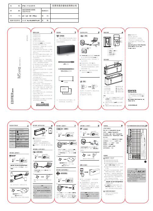
M5MK 多媒体有源音响 3.5mm-3.5mm音频线 使用说明书
3.5mm-3.5mm音频线
收纳袋
版面设计:
版本号及料号: V1.0/ 名 称: M5MKII中文说明书材 质:
尺 寸: 40×140(MM)R=8mm 校 对:批 准:
东莞市漫步者科技有限公司
USB连接线
售后服务卡
说明书
注:本说明书中的图片均为示意图,可能 与实物有偏差,请以实物为准。
③
开机、蓝牙连接/断开、电池电量低时,系统将发出提示音。
当音量调至最大时,继续按“+”键,
音响会发出“咚…”的提示音。
电池使用时间(本机充满电后,在蓝牙模式下可连续播放约12小时)因音源和音量调节会有所差异。
7
②
②
将U盘插入USB接口,连接成功后LED灯为红色。
系统自动播放U盘中的音乐(仅支持MP3/WMA格式),最大支持 32GB
的U盘。
操作指南(U盘模式)
操作指南(备用电源输出)
①
红色闪烁
红色
①
红色闪烁
80克欧维斯米黄纸折页不打钉
音响
------短按:上/下一曲
本机的USB接口可对外提供5V/最大500mA 的直流电源输出,可对小型移动设备供电、充电。
将USB连接线的一端接音箱DC OUT 接口,另一端接需充、供电设备的USB接口。
备用电源输出
U盘输入
本机具有NFC近场通讯功能,当手持蓝牙设备也有NFC功能,开启后,近距离贴近主机端面LED灯处时,会自动与主IB-100-M0005H-00 播放/暂停
------长按:上/下一目录------。
KL26P64M48SF5 中文资料
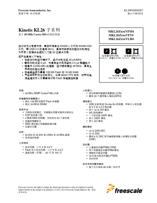
定时器 • 六通道定时器/PWM (TPM) • 两个双通道定时器/PWM 模块 • 周期性中断定时器 • 16 位低功耗定时器(LPTMR) • 实时时钟
安全性和完整性模块 • 每个芯片具有 80 位唯一标识号
Freescale reserves the right to change the detail specifications as may be required to permit improvements in the design of its products. © 2013–2014 Freescale Semiconductor, Inc. 保留
所有权利。
器件型号
MKL26Z32VFM4 MKL26Z64VFM4 MKL26Z128VFM4 MKL26Z32VFT4 MKL26Z64VFT4 MKL26Z128VFT4 MKL26Z32VLH4 MKL26Z64VLH4 MKL26Z128VLH4
Flash (KB) 32 64 128 32 64 128 32 64 128
• 在极低功耗运行模式下,运行功耗低至 40 μA/MHz • 静态功耗低至 2 μA,并具有全状态保留和 4.5 μs 唤醒能力 • 超高效 Cortex-M0+处理器,运行频率高达 48 MHz,具有业
界领先的吞吐速率 • 存储器选项为最高 128 KB Flash 和 16 KB RAM • 节能架构针对低功耗优化,采用 90nm TFS 技术、时钟和电
3 外设工作要求与特性......................................................................17 3.1 内核模块................................................................................. 17 3.1.1 SWD 电气特性 ......................................................... 17 3.2 系统模块................................................................................. 18 3.3 时钟模块................................................................................. 18 3.3.1 MCG 特性.................................................................. 18 3.3.2 振荡器电气规格........................................................ 20 3.4 存储器和存储器接口............................................................. 22 3.4.1 Flash 电气规格...........................................................22 3.5 安全性和完整性模块............................................................. 23 3.6 模拟......................................................................................... 24 3.6.1 ADC 电气规格...........................................................24 3.6.2 CMP 和 6 位 DAC 的电气规格................................ 28
HPMLDL系列服务器

HPMLDL系列服务器hpML系列服务器HP ProLiant ML110G7(C8R00A)参数规格差不多参数产品类型工作组级产品类别塔式产品结构4U处理器CPU类型奔腾双核CPU型号奔腾双核G860CPU频率3GHzHP ProLiant ML330 G6(600911-AA1)参数规格差不多参数产品类型企业级产品类别塔式产品结构5U处理器CPU类型Intel 至强5600CPU型号Xeon E5620CPU频率 2.4GHz智能加速主2.666GHz频标配CPU1颗数量最大CPU2颗数量制程工艺32nm三级缓存12MB总线规格QPI 5.86GT/sCPU核心四核HP ProLiant ML330 G6(B9D22A)参数规格差不多参数产品类型企业级产品类别塔式产品结构5U处理器CPU类型Intel 至强5600 CPU型号Xeon E5606CPU频率 2.13GHz标配CPU1颗数量最大CPU2颗数量制程工艺32nm三级缓存8MB总线规格QPI 4.8GT/sHP ProLiant ML330 G6(600911-AA1)参数规格差不多参数产品类型企业级产品类别塔式产品结构5U处理器CPU类型Intel 至强5600CPU型号Xeon E5620CPU频率 2.4GHz智能加速主2.666GHz频标配CPU1颗数量最大CPU2颗数量制程工艺32nm三级缓存12MB总线规格QPI 5.86GT/sCPU核心四核HP ProLiant ML350 G6(638180-AA1)参数规格差不多参数产品类别塔式产品结构5U处理器CPU类型Intel 至强5600CPU型号Xeon E5606CPU频率 2.13GHz标配CPU1颗数量最大CPU2颗数量制程工艺32nm三级缓存8MB总线规格QPI 4.8GT/sCPU核心四核CPU线程四线程数主板HP ProLiant ML350 G6(600431-AA5)参数规格差不多参数产品类别塔式产品结构5U处理器CPU类型Intel 至强5600CPU型号Xeon E5620CPU频率 2.4GHz智能加速主2.666GHz频标配CPU1颗数量最大CPU2颗数量制程工艺32nm三级缓存12MB总线规格QPI 5.86GT/sCPU核心四核CPU线程八线程数HP ProLiant ML350 G6(594869-AA1)参数规格差不多参数产品类别塔式产品结构5U处理器CPU类型Intel 至强5600CPU型号Xeon E5620CPU频率 2.4GHz智能加速主2.666GHz频标配CPU1颗数量最大CPU2颗数量制程工艺32nm三级缓存12MB总线规格QPI 5.86GT/sCPU核心四核CPU线程八线程数HP ProLiant ML310e Gen8(686146-AA5)参数规格差不多参数产品类型企业级产品类别塔式产品结构4U处理器CPU类型Intel 至强E3-1200 v2 CPU型号Xeon E3-1220 v2CPU频率 3.1GHz标配CPU1颗数量最大CPU4颗数量制程工艺22nm三级缓存8MB总线规格DMI 5GT/sHP ProLiant ML310e Gen8(686147-AA5)参数规格差不多参数产品类型企业级产品类别塔式产品结构4U处理器CPU类型Intel 至强E3-1200 v2 CPU型号Xeon E3-1240 v2CPU频率 3.4GHz智能加速主3.8GHz频标配CPU1颗数量最大CPU4颗数量制程工艺22nm三级缓存8MBHP ProLiant ML350e Gen8(C3Q10A)参数规格差不多参数产品类型企业级产品类别塔式产品结构5U处理器CPU类型Intel 至强E5-2400 CPU型号Xeon E5-2403CPU频率 1.8GHz标配CPU1颗数量最大CPU4颗数量制程工艺32nm三级缓存10MB总线规格QPI 6.4GT/sHP ProLiant ML350e Gen8(C3Q08A)参数规格差不多参数产品类型企业级产品类别塔式产品结构5U处理器CPU类型Intel 至强E5-2400 CPU型号Xeon E5-2407CPU频率 2.2GHz标配CPU1颗数量最大CPU4颗数量制程工艺32nm三级缓存10MB总线规格QPI 6.4GT/sHP ProLiant ML350e Gen8(C3Q09A)参数规格差不多参数产品类型企业级产品类别塔式产品结构5U处理器CPU类型Intel 至强E5-2400 CPU型号Xeon E5-2420CPU频率 1.9GHz标配CPU1颗数量最大CPU4颗数量制程工艺32nm三级缓存15MB总线规格QPI 6.4GT/sHP ProLiant ML350e Gen8(C3F91A)参数规格差不多参数产品类型企业级产品类别塔式产品结构5U处理器CPU类型Intel 至强E5-2400 CPU型号Xeon E5-2430CPU频率 2.2GHz标配CPU1颗数量最大CPU4颗数量制程工艺32nm三级缓存15MB总线规格QPI 6.4GT/sHP ProLiant ML350p Gen8(646675-AA1)参数规格差不多参数产品类别塔式产品结构5U处理器CPU类型Intel 至强E5-2600 CPU型号Xeon E5-2609CPU频率 2.4GHz标配CPU1颗数量最大CPU2颗数量制程工艺32nm三级缓存10MB总线规格QPI 6.4GT/sHP ProLiant ML350p Gen8(668271-AA5)参数规格差不多参数产品类别塔式产品结构5U处理器CPU类型Intel 至强E5-2600 CPU型号Xeon E5-2620CPU频率2GHz智能加速主2.5GHz频标配CPU1颗数量最大CPU2颗数量制程工艺32nm。
PLA 85 说明书

50119511 G1 Valid from 2018 week 46PLA 85Pos. No. Varebetegnelse Description of goods WarenbezeichnungDésignation des pièces80690085 Plasmaslange med centraltilslutning, 6m Plasma torch with central adaptor plug, 6m Plasmaschlauch mit Zentralanschluss, 6m Torche plasma avec raccordement central, 6m 1 45050101 TastTrigger Taster Gâchette 2 71610194 Monteret print PCBPlatine Circuit imprimé montée 3 80600096 VippearmTipping device Kippvorrichtung Dispositif à bascule 4 80600092 Håndtag Handle HandgriffPoignée5 80600098 Skruer for håndtag (1 sæt = 5 stk)Screw for handle (1 set = 5 pcs) Schraube für Handgriff (1 Satz = 5 Stück) Vis pour poignée (1 jeu = 5 pièces) 6 80600097 Kontaktstift Contact pin Kontaktstift Fiche de contact 7 80650005 Brænderhoved Torch body Brennerkörper Corps de torche 7a 80600018 Gasrør Gas tube Gasrohr Tubeà gaz 8 80610005 Elektrode Electrode Elektrode Electrode9 80630009 Dyse 1,2 mm Nozzle 1.2 mm Düse 1,2 mm Buse 1,2 mm 9 80630010 Dyse 1,4 mm Nozzle 1.4 mm Düse 1,4 mmBuse 1,4 mm 10 80630011 Beskyttelseskappe Protective capSchutzkappe Bague de protection 11 80600088 Afstandsfjeder Distance spring AbstandsfederRessort de distance 12 80600101 Afstandsbøjle (2 ben)Distance ring (2 legs)Distanzbügel (2 Schenkel) Dispositif de distance (2 pied)12A 80600108 Afstandsbøjle Distance ringDistanzbügel Dispositif de distance 13 24510237 NøgleKey Universalschlüssel Clef14 82034014 GasflowmeterGas flowmeter GasdurchflußmesserDébitmètre de gaz15 80680085 Slangemodul PDX 85 m/ZA, 6mHose module PDX 85 with ZA, 6mSchlauchmodul PDX 85 with ZA, 6m Module de torche PDX 85 avec ZA, 6m 16 45070007 Slangeaflastning ø35 Hose protection ø35Schlauchentlastung ø35 Douille isolate de cable ø3517 40110406 CHJ skrue M4x6CHJ screw M4x6 Zylinderkopfschraube M4x6 Vis CHJ screw M4x618 25450047 Aflastningsring Relief-ringEntlastungsringBague d’allègement 19 80200335 Møtrik til ZA, plastik Nut for ZA, plasticMutter für ZA, Plastik Écrou pour ZA, plastique 20 80300601 Centraltilslutning Central adaptor plug ZentralsteckerFiche de contact 21 80300603 Hanstik kontaktdel Male contact partKontaktteil männlich Partie de contact, mâle 21a 80300602 Hanstik til ledningMale pin for wireKontaktteil für Leitung, männlich Connecteur mâle (câble)22 80600091 Cirkelslag kompletCircle cutting device completeKreisschneide-Einrichtung komplett Support pour coupe circulaire complet 22A 80600094 Stang for cirkelslagRadius arm for circle cutting device Führungsstang für Kreisschneide-Einrichtung Bras support pour coupe circulaire 22B 80600090 Brændervogn (drejebar) Torch carriage (revolving) Brennerwagen (drehbar) Support torche (pivotant)23 80600093 Brændervogn (fast) Torch carriage (fixed)Brennerwagen (fest)Support torche (fixe)。
施耐德Modicon M258可编程控制器产品目录
M258 可编程控制器都标配 4 路电压或电流模拟量输入 (12 位分辨率)。
<பைடு நூலகம்温度控制
此外还提供2、4或6通道以及12或16位不同分辨分辨率的扩展模块。 M258可编程控制器性能强大,能够连接多达200个模拟量I/O和/或温度模块,从而减
2
少了对设备需求的限制。
模拟量控制功能
< 速度控制
最多8通道高速 计数
软件组态
所有 M258
置和编程功能旨在降低成本和优化设备性能。
SoMachine 软件支持六种 IEC 61131-3 编程语言: v IL (指令表) v LD (梯形图) v SFC (顺序功能块) v ST (结构文本) v FBD (功能块图) v CFC (连续功能图)
另外还支持 PLCopen 功能块,以管理设备的运动控制和轴控制。
4个控制器状态ledrunmsbatteryapp0app16个内置通信端口状态ledethlaethstethnsusbhostmbscomcansts用于在5对称导轨上安装卸载的锁扣两个用于通信模块的pci闲置插槽带有可插拔接线端子和锁扣显示块和标签插槽的24电源模块io模块每个模块都具有带锁扣的可插拔接线端子显示io状态的显示块和标签夹持器插槽带上锁解锁功能的锁扣的可插拔接线端子在侧面用于连接下一个模块的总线扩展连接器rtc实时时钟电池插槽连接usb存储卡用于传输程序数据或固件更新的usba连接器标记为host用于连接编程计算机的usbb微型连接器标记为pgrport用于连接以太网和或magelisxbtgt图形终端的rj45连接器标记为ethernet用于连接rs232或rs485串行链路的rj45连接器标记为mbs9芯subd公头连接器标记为can0用于连接canopen总线仅限tm258lf42dt4ltm258lf42drtm258lf66dt4l1011
01. Introduction to M580 - CN

● EtherNet/IP ● Modbus/TCP
● BME 模块的功能类似于已经在M340 PLC中使用的BMX NOC
● BME NOC 03*1 模块已经内置了网络安全功能,用来提高 在M580架构中抵御网络攻击的能力
12
远程子站适配器- BME CRA 312 10
● 与背板的双连接:
● X-Bus (1) ● 以太网 (2)
● 适配孔可以防止模块安装在BMX的老 机架上 (3)
M580 Configuration V1.0
Schneider Electric | Industry Business | Training | March 20, 2020
描述 4槽以太网背板 8槽以太网背板 12槽以太网背板
Ethernet & X-Bus 槽数 4
8
8
仅X-Bus 槽数 0 0 4
● 在M580架构中,以太网背板在任何时候都不能被用于扩展机架
M580 Configuration V1.0
Schneider Electric | Industry Business | Training | March 20, 2020
15
HART 模块 – BME AH* 0*12
● 提供2个HART 模块, 这些是应用新以太网背板的第一个新X80模块 :
● BME AHI 0812 – 8 通道模拟量输入模块 4 – 20 mA ● BME AHO 0412 – 4 通道模拟量输出模块 4 – 20 mA
电子白板
电
子
扫
描
板
产品型号
功能简介
UB8325
标准幅面(9001400)\投影白板双模式\专业投影屏\交互控制\网络会议\普通纸打印\A4纸输出\超生波、红外线定位\彩色电子笔\电子板擦\落地支架
UB-518B
标准幅面(9001400)\两屏循环\热敏打印\双面缩印\CCD感应\A4纸输出\对比度可调\8点/mm精度\多页复印\12s/页速度\33kg\笔擦套装\落地支架\金属外框\集成USB1.1电脑接口
UB-528P
标准幅面(9001400)\两屏循环\普通纸打印\双面缩印\CCD感应\A4纸输出\对比度可调\8点/mm精度\多页复印\15s/页速度\34kg\笔擦套装\落地支架\金属外框\集成USB1.1电脑接口
UB-628P
加宽幅面(9001762)\两屏循环\普通纸打印\双面缩印\CCD感应\A4纸输出\对比度可调\8点/mm精度\多页复印\15s/页速度\36kg\笔擦套装\落地支架\金属外框\集成USB1.1电脑接口
大连信开数码成都分公司
UB-618B
加宽幅面(9001762)\两屏循环\热敏打印\双面缩印\CCD感应\A4纸输出\对比度可调\8点/mm精度\多页复印\12s/页速度\37kg\笔擦套装\落地支架\金属外框\集成USB1.1电脑接口
标准幅面(9001400)\四屏循环\热敏打印\双面缩印\CCD感应\A4纸输出\对比度可调\8点/mm精度\多页复印\12s/页速度\35kg\笔擦套装\落地支架\金属外框\集成USB1.1电脑接口
UB-728P
标准幅面(9001400)\四屏循环\普通纸打印\双面缩印\CCD感应\A4纸输出\对比度可调\8点/mm精度\多页复印\15s/页速度\38kg\笔擦套装\落地支架\金属外框\集成USB1.1电脑接口
WBT-851说明书

重要提示
感谢您使用许继电气股份有限公司的产品。为了安全、正确、高效地使用本装置,请您务必注意以下重要提示:
本说明书仅适用于WBT-851微机备自投保护装置。
请仔细阅读本说明书,并按照说明书的规定调整、测试和操作。如有随机资料,请以随机资料为准。
b.冲击响应:装置能承受GB/T 14537-1993中4.2.1规定的严酷等级为I级冲击响应检验。
c.振动耐久:装置能承受GB/T 11287-2000中4.2.2规定的严酷等级为I级振动耐久检验。
d.冲击耐久:装置能承受GB/T 14537-1993中4.2.2规定的严酷等级为I级冲击耐久检验。
2.6
a.绝缘电阻:各带电的导电电路分别对地(即外壳或外露的非带电金属零件)之间,交流回路和直流回路之间,交流电流回路和交流电压回路之间,用开路电压为500V的测试仪器测试其绝缘电阻值不应小于100MΩ。
b.介质强度:装置通信回路和24V等弱电输入输出端子对地能承受50Hz、500V(有效值)的交流电压,历时1min的检验无击穿或闪络现象;其余各带电的导电电路分别对地(即外壳或外露的非带电金属零件)之间,交流回路和直流回路之间,交流电流回路和交流电压回路之间,能承受50Hz、2kV(有效值)的交流电压,历时1min的检验无击穿或闪络现象。
1
采用Nucleus Plus公司的实时多任务操作系统
装置的实时性、可靠性和运行的稳定性高
采用分层的设计方案
采用模块化设计方案,便于配置
软件的升级方便
完善的软件测试方案
1
遥测采集回路自检
开出回路自检,可以到继电器动作线圈
AD、RAM、EPROM芯片自检
玛田音箱中文文档1.0

P4玛田音响威风系列W8L是线性阵列音响系统,将革新号角负载技术与线性阵列科技融为一体,可产生强烈动感冲击力的阵列音响效果。
它是三分频全音域音响系统,无需低音单元配合也可适用于多种应用范围。
在需要低频扩伸的地方,W8L可与玛田WSX/WLX 折叠式号角的低音单元配合使用,成为完全号角负载的四分频音响配置。
W8LC是紧凑型线性阵列系统,专为演唱会、剧院和商业宣传活动提供超级新生代线性阵列音响效果而设计。
它可以满足大功率、强劲的低音冲击效果系统的需要,应用范围相当广泛,可应用于现场播音、团体活动和固定安装。
W8LC的网格结构还可根据需要进行吊挂安装或地面叠放安装。
它是全频音响系统,在许多应用情况中,不需要配合低音单元也能使用。
它还可以配合吊挂式的WLX或地面叠放式WLX/WSX低音单元使用。
P5W8LM迷你型线性阵列外围设备,专为需要阵列效果的中小型规模应用而设计。
它是用途广泛、可升级的音响系统,可用作吊挂安装或地面叠放,适用于团体活动、剧院和室内活动;同时也可作为大规模户外音响系统的声音延迟系统。
继承W8L和W8LC的恒定指向号角设计,W8LM是三分频音响系统,将创新号角技术与小型线性阵列技术融为一体,可充分发挥小型线性阵列音响的最大动感震憾效果,产生新一代音响效果。
它可与WLX号角负载的低音单元配合,吊挂安装使用。
加W8L的低频音响输出而设计。
W8LS的大小与W8L相同,并且具备相同的专用安装系统,为吊挂安装提供快捷安全的安装方案。
它具备1000瓦18“双驱动单元,磁性结构和吊挂驱动可产生最大的线性振幅,从而产生低沉浑厚的低音。
P6术。
是WSX的附属音响,WLX体积较小、重量较轻,可与W8线性阵列系统配合使用,既可吊挂安装也可于地面叠放,可以低频延展拥有高输出的音质效果。
单独特长距振幅18”(460毫米)/4”(100毫米)音圈驱动器是通过低flare rate 的双曲线号角在箱体前部负载。
驱动器后面是反射负载,可将低频输出延展低于号角的分频点。
领航者wifi性能参数

高效防火墙
提供IP与MAC地址自动扫描及绑定功能,有效遏制内网ARP病毒攻击,可有效防范各种常见的DoS攻击、扫描类攻击、ARP病毒、可疑包攻击行为。
USB灵活扩展
通过USB扩展接口,可以随时随地共享,轻松实现有线和无线打印,让您的办公发生革命性的变化,节约企业投资成本还提高工作效率。
支持3G无线上网卡(部分型号支持)。
灵活接入
支持ADSL或光纤线路接入,具有电信\联通\教育网的智能策略路由,线路智能负载均衡功能,有效提高带宽利用率。
虚拟专网(VPN)
BCM4706,600MHz
Flash/DRAM内存
16M/64M
8M/ห้องสมุดไป่ตู้4M
8M/64M
8M/128M
无线参数
2.4G,300M
2.4G,300M
2.4G/5.8G,600M
2.4G,450M
接口
1个100M自适应RJ45 WAN端口
4个100M自适应RJ45 LAN端口
1个USB2.0标准接口
1个100M自适应RJ45 WAN端口
4个100M自适应RJ45 LAN端口
1个100M自适应RJ45 WAN端口
4个100M自适应RJ45 LAN端口
1个USB2.0标准接口
1个100M自适应RJ45 WAN端口
4个100M自适应RJ45 LAN端口
1个USB2.0标准接口
产品尺寸
7寸金属壳
7寸金属壳
7寸金属壳
294*178.8*44(mm)金属壳
领航者智能WIFI营销系统WJ800/850/860/880
S500型号快速作用低断电容量电感说明书
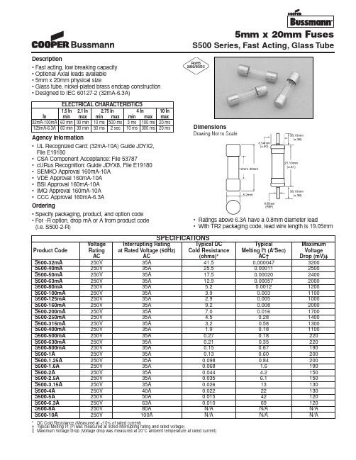
Description•Fast acting, low breaking capacity •Optional Axial leads available •5mm x 20mm physical size•Glass tube, nickel-plated brass endcap construction •Designed to IEC 60127-2 (32mA-6.3A)Agency Information•UL Recognized Card:(32mA-10A) Guide JDYX2, File E19180•CSA Component Acceptance:File 53787•cURus Recognition:Guide JDYX8, File E19180•SEMKO Approval 160mA-10A •VDE Approval 160mA-10A •BSI Approval 160mA-10A •IMQ Approval 160mA-10A •CCC Approval 160mA-6.3A Ordering•Specify packaging, product, and option code •For -R option, drop mA or A from product code (i.e.S500-2-R)•Ratings above 6.3A have a 0.8mm diameter lead•With TR2 packaging code, lead wire length is 19.05mmDimensionsDrawing Not to ScaleSPECIFICATIONSVoltage Interrupting Rating Typical DC TypicalMaximum Product Code Rating at Rated Voltage (50Hz)Cold ResistanceMelting I 2t (A 2Sec)Voltage AC AC (ohms)*AC†Drop (mV)‡S500-32mA 250V 35A 41.50.0000473200S500-40mA 250V 35A 25.50.000112500S500-50mA 250V 35A 17.50.000202400S500-63mA 250V 35A 12.90.000572000S500-80mA 250V35A 5.20.00121200S500-100mA 250V 35A 3.90.0031100S500-125mA 250V 35A 2.90.0051000S500-160mA 250V 35A 9.20.0082000S500-200mA 250V 35A 7.00.0161700S500-250mA 250V 35A 4.50.281400S500-315mA 250V 35A3.20.581300S500-400mA 250V 35A 1.90.181100S500-500mA 250V 35A 0.270.18220S500-630mA 250V 35A 0.210.35220S500-800mA 250V 35A 0.150.67190S500-1A 250V 35A 0.130.60200S500-1.25A 250V 35A 0.0980.84200S500-1.6A 250V 35A 0.068 1.6190S500-2A 250V 35A 0.0444.2150S500-2.5A 250V 35A 0.035 6.1150S500-3.15A 250V 35A 0.02613130S500-4A 250V 40A 0.02222130S500-5A 250V 50A 0.01542120S500-6.3A 250V 63A 0.01069120S500-8A 250V 80A N/A N/A N/A S500-10A250V100AN/AN/AN/A*DC Cold Resistance (Measured at <10% of rated current)†T ypical Melting I 2t (I 2t was measured at listed interrupting rating and rated voltage)‡Maximum Voltage Drop (Voltage drop was measured at 20°C ambient temperature at rated current)5mm x 20mm FusesS500 Series,Fast Acting,Glass TubeRoHS 2002/95/ECTIME CURRENT CURVEPACKAGING CODEPackaging CodeDescriptionBK 100 pieces of fuses packed into a cardboard carton BK11,000 pieces of fuses packed into a poly bagTR21,500 pieces of fuses packed into tape on a reel (19.05mm lead wire length)OPTION CODEOption CodeDescriptionV Axial leads - copper tinned wire with nickel plated brass overcaps -RRoHS compliant version5mm x 20mm FusesS500 Series,Fast Acting,Glass TubeVisit us on the web at: OC-2569 3/07©Cooper ElectronicTechnologies 2007Cooper Electronic Technologies 1225 Broken Sound Parkway NW Suite F Boca Raton, FL 33487-3533Tel: 1-561-998-4100Fax: 1-561-241-6640Toll Free: 1-888-414-2645Cooper Bussmann P .O. Box 14460St. Louis, MO 63178-4460Tel: 1-636-394-2877Fax: 1-800-544-2570Cooper Electronic Technologies Cooper (UK) Limited Burton-on-the-Wolds Leicestershire • LE12 5TH UK Tel: +44 (0) 1509 882 737Fax: +44 (0) 1509 882 786Cooper Electronic Technologies Avda. Santa Eulalia, 29008223Terrassa, (Barcelona), Spain Tel: +34 937 362 812+34 937 362 813Fax: +34 937 362 719Asia PacificCooper Electronic Technologies 1Jalan Kilang Timor#06-01 Pacific Tech Centre Singapore 159303Tel: +65 278 6151Fax: +65 270 4160North AmericaEurope。
梦派85寸教育触摸一体机

梦派85寸教育触摸一体机一、壁挂款式:二、产品参数:规格参数液晶面板参数型号85L1屏LED显示屏规格1927.99 mm×1153.31 mm×99.7 mm 分辨率3840*2160色彩16.7M亮度400cd/㎡对比度5000:1可视角度±178°反应时间5ms灯管寿命60,000(hrs)设备接口Tuner×1; HDMI接口×2;VGA in×1;USB×2;ethernet×1;wifi×1;earphone ×1;AV-out ×1;SD-card×1;YPbPr in×1;AV-in×1;UART×1;SPDIF out×1;USB(触摸) ×1;支持ATV/DTV;多媒体音视频;CVBS;支持中文简体、英文。
主板系统参数CPU MSTAR MSD6A828 四核Cortex 1.4GHZ RAM 4G/8G DDR3FLASH 8GBSD card 最大支持128GBAndroidversion5.0高清HDMI 2.0端子USB X 2PC 配置(选配)CPU支持Intel Core I3内存条DDR3 4G/8G (可选)硬盘SATA 320G/SATA500G/固态硬盘SSD(128G) (可选)接口HDMI×1,VGA×1,USB2.0×2,USB3.0×2,RJ×1,I/O接口×1,PS/2×1主板H81芯片组显卡显卡集成声卡声卡集成操作系统Windows 7/ Windows 8触摸屏触摸技术红外感应触摸技术(非外挂)书写方式手指、笔或其它任何非透明物体响应时间4ms定位精度±1.5mm分辨率4096×4096有效识别>5mm通信方式全速USB触摸点数10点三、产品特性:1、采用高质量红外触摸面板,超高透光率,抗暴能力强,耐刮耐磨。
华为4K电视85说明书
华为4K电视85说明书
1、首先接通电源之后开机,同时按下遥控器上的主页键和菜单键与华为4K电视85号完成配对。
使用华为手机扫描屏幕二维码登录华为账号(或者手动输入账号和密码登录)。
2、进入主页面后,智慧屏菜单以横置排列栏目,从左到右有【我家】、【首页】、【VIP】、【电视剧】、【电影】等分类。
进入某一个分类可以选择功能和查看影视节目,其中【我家】是可以进入AI健身、视频通话、智能家居控制等功能。
【首页】可以进入应用等功能。
3、如果您使用的是华为或荣耀带有NFC的手机,可以通过下载智慧屏APP。
把手机靠近遥控器下方的NFC触控区域实现智慧跨屏,在手机上可以实现投屏、远程控制等功能。
其他品牌手机在连接到与智慧屏同一个WiFi后,可以开启自带的投屏功能与智慧屏连接。
4、查看和控制智能设备,在智慧屏【首页】选择【全部应用】-【智能家居】,就能查看使用相同的华为帐号登录,且已添加的智能家居设备
及其工作状态,还可以使用遥控器快捷控制部分智能设备。
施耐德指导笔记

施耐德指导笔记施耐德培训笔记一、M580系列硬件简介1.M580是施耐德第一款基于全以太网技术的可编程自动化控制器(ePAC),2.M580系列硬件方面有9款不同性能CPU,型号代码为BM E P58XXYY(YY为40型号的可以接远程I/O子站,最大数量为31个)。
M580内存比较大,如果需要配置内存卡,需用施耐德提供的内存卡(M340内存卡能用于M580上)。
3.M580CPU包含三个以太网口(1个服务口,2服务口HMI等)设备口用于:①分布式I/O4.M580系列推出了新的以太网背板CRA。
以太网机架任何时候都不能用于扩展机架。
Ethernet的I/O0号槽位。
5.开始,后两位为MAC地址最后2个字节(转。
6.,只支持通讯模块和嵌入式的开关模块。
RIO或DIO)类型I/O、远程I/O、以太网I/O。
2.I/O采用总线/网络通信,性能中等,I/O远但数据交换容量小。
以太网I/O采用以太网通信,性能高,距离远,有利于分布式设备集成。
3.在使用超五类屏蔽双绞线或更好的电缆的情况下,各以太网远程I/O子站之间的距离不能超过一百米。
若子站间距离超过100米,一种方案是添加光纤中继模块BMXNRP解决此问题。
使用NRP时,必须是CRA模块与NRP模块互联。
采用光纤,通信距离可达到15公里。
另一种方案使用双环网交换机(DRS)。
三、冗余配置1.两个冗余型号M580CPU(型号中有H表示为冗余型号)2.两块电源模块及以太网背板3.同步接头(有光纤接头NAC0201或屏蔽双绞线接头NAC0100)。
同步电缆采用六类或七类线,同步速率可到1GBit。
4.在软件配置时,热备IP地址不能编辑,为主IP地址+1。
主备切换时,不会影响主备CPU的IP地址。
5.冗余CPU背后有一个旋钮开关,可以设置CPU为A端或B端或清除程序。
四、UnityPro1.变量导入导出工具:开始—>SchneiderElectric—>UnityPro—>Extras—可以方便进行大量变量的创建与导入。
无刷电机控制器
嵌入式 MCU
兼容 MCS®51 指令执行周期 63%< 3 个系统时钟 (3T) 内存大小:
12KB 闪存程序存储器 256+1 KB SRAM 数据存储器 扩展的 16 位乘/除单元 (MDU) ≤17 个通用输入/输出 (GPIO) 引脚 全双工的串行接口 (UART) I2C 接口 串行外围接口 (SPI) 三个外部中断 三个 16 位计时器 可编程 15 位看门狗计时器 (WDT) 内置上电复位 (POR) 内置时钟发生器 两级程序存储器锁定
三级过流保护 (OCP)
电源管理
空闲模式、停止模式和睡眠模式
开发支持
系统内编程 (ISP) 片上调试支持 (OCDS)
© 2013 Fairchild Rev. 1.0.0 • 4/14/14
AN-8202
应用指南
图 1.
应用模块图
8 通道 10 位 ADC
- 自动触发采样并保持 - 四个触发模式选择 - 三个前置放大器增益选择 1 通道 8 位 DAC
保护
可配置处理内核
- 采用速度积分法的无传感器 FOC - 带滑动模式的无传感器磁场定向控制 - 霍尔接口 空间向量调制 (SVM) 正弦波和方波发生器 可编程电流前沿相位控制 可编程死区时间
AN-82பைடு நூலகம்2
FCM8531 用户手册硬件说明
1. 概括
FCM8531 是一款用于电机控制的特定应用的双核心处 理器,由先进电机控制器 (AMC) 处理器和与 MCS®51 兼容型的 MCU 处理器组成。AMC 是专门为电机控制 设计的核心处理器,并且还专门集成了可配置处理内核 和外围电路以执行无传感器磁场定向控制 (FOC) 电机控 制。可通过用于不同电机应用的嵌入式 MCS®51 对系统 控制、用户界面、通信接口和输入/输出接口编程。 FCM8531 双核心处理器的优点是,这两个处理器可独 立工作且相互补充。 AMC 专用于电机控制应用,如电 机控制算法、PWM 控制、电流感测、实时过流保护和 电机相角计算。嵌入式 MCU 向 AMC 提供电机控制命 令,以通过通信接口控制电机。由于在 AMC 中执行了 复杂的电机控制算法,所以此方法可以减少软件的负担 并简化控制系统程序。Fairchild 为用户提供电机控制开 发系统 (MCDS) IDE 和 MCDS 编程套件以进行软件开 发,执行系统内编程 (ISP),并执行在线调试。 图 1 说明 FCM8531 的典型应用。 ADC 和 DAC 先进电机控制器 (AMC)
智能蓄电池内阻测试仪使用说明书

NRBT-8850 智能蓄电池内阻测试仪产品说明书武汉南瑞西高电气实业有限公司目录一、概述 (3)1.1 用途 (3)1.2 特点 (3)1.3 技术指标 (3)1.4 仪表基本功能 (4)二、操作指导 (5)2.1 仪表开机/关机 (5)2.2 主菜单 (5)2.3 电池测量功能 (5)2.3.1 单节电池测量 (5)2.3.2 成组电池测量 (6)2.4 示波器功能 (6)2.5 数据管理功能 (6)2.6 系统管理 (7)2.6.1 时间设置 (7)2.6.2 参数校准 (8)2.6.3 系统更新 (11)2.6.4 语言选择 ........................................................................................ 错误!未定义书签。
2.6.5 版本信息 ........................................................................................ 错误!未定义书签。
三、仪器结构 (13)四、仪表存储说明 (14)五、日常维护 (15)六、常见问题解答 (16)一、概述1.1 用途智能蓄电池内阻测试仪主要用来测试蓄电池内阻,通过内阻值来评估蓄电池好坏,从而作为蓄电池管理参考依据。
1.2 特点●设计小巧,重量轻,方便使用者携带及操作;●仪器功能:单节电池测量、成组电池测量、示波器;●既可以采用按键操作也可以采用触摸屏操作。
1.3 技术指标测量范围:内阻:0.0mΩ--100mΩ电压:0.000v--16v最小测量分辨率内阻:0.01 mΩ电压:1mV测量精度内阻:±2.0%rdg ±6dgt电压:±0.2%rdg ±6dgt显示屏:240×320 24bit 3.5寸TFT LCD + 触摸屏内存容量:16 M字节FLASH外部存储接口:USB (可插接U盘)工作电源:可充电锂电池,充满可工作5~6小时外接电源:AC100~240V/DC8.4V-1A 电源适配器/充电器1.4 仪表基本功能序号项目描述1 电池测量可进行单节电池、成组电池的内阻测量及性能评估。
- 1、下载文档前请自行甄别文档内容的完整性,平台不提供额外的编辑、内容补充、找答案等附加服务。
- 2、"仅部分预览"的文档,不可在线预览部分如存在完整性等问题,可反馈申请退款(可完整预览的文档不适用该条件!)。
- 3、如文档侵犯您的权益,请联系客服反馈,我们会尽快为您处理(人工客服工作时间:9:00-18:30)。
4194304-BIT (524288-WORD BY 8-BIT)CMOS STATIC RAMM5M5V408B## -85LWM5M5V408B## -10LW M5M5V408B## -85HW M5M5V408B## -10HW M5M5V408B## -85L M5M5V408B## -10L M5M5V408B## -85H M5M5V408B## -10H M5M5V408B## -85LIM5M5V408B## -10LI M5M5V408B## -85HI M5M5V408B## -10HIStandard 0 ~ +70°CW-version -20~ +85°CI-version -40 ~ +85°CVersion,Part name(## stands for "FP","TP","RT","KV"or"KR")Power SupplyAccess time max.25°C Stand-by current Icc (PD), Vcc=3.0V 85ns 2.7 ~ 3.6V 2.7 ~ 3.6V 2.7 ~ 3.6V 2.7 ~ 3.6V 2.7 ~ 3.6V 2.7 ~ 3.6V---------0.3µA 0.3µA 0.3µA ---1µA 1µA 3µA 1µA3µAtypical *---------40°C 1µA 1µA 1µA------20µA 10µA20µA 10µA 40µA 20µA 20µA 10µA 40µA 20µA70°C 85°C 25°C 40°C ---------------3µA 100ns85ns 100ns 85ns 100ns 85ns 100ns 85ns 100ns 85ns 100nsDESCRIPTION• Single +2.7~+3.6V power supply • Small stand-by current: 0.3µA(3V,typ.)• No clocks, No refresh• Data retention supply voltage=2.0V to 3.6V • All inputs and outputs are TTL compatible.• Easy memory expansion by S • Common Data I/O• Three-state outputs: OR-tie capability• OE prevents data contention in the I/O bus • Process technology: 0.25µm CMOS • Package:M5M5V408BFP: 32 pin 525 mil SOPM5M5V408BTP/RT: 32 PIN 400mil TSOP(ll)M5M5V408BKV/KR: 32 pin 8mm x13.4mm STSOPFEATURESActive current 30mA (10MHz)5mA (1MHz)Ratings (max.)Operating temperatureThe M5M5V408B is a family of low voltage 4-Mbit static RAMs organized as 524,288-words by 8-bit, fabricated by Mitsubishi's high-performance 0.25µm CMOS technology.The M5M5V408B is suitable for memory applications where a simple interfacing , battery operating and battery backup are the important design objectives.M5M5V408B is packaged in 32-pin plastic SOP, 32-pin plastic TSOP and 32-pin 8mm x 13.4mm STSOP packages. Two types of TSOPs and two types of STSOPs are available, M5M5V408BTP (normal-lead-bend TSOP), M5M5V408BRT (reverse-lead-bend TSOP), M5M5V408BKV (normal-lead-bend STSOP) and M5M5V408BKR (reverse-lead-bend STSOP). These two types TSOPs and two types STSOPs are suitable for a surface mounting on double-sided printed circuit boards.From the point of operating temperature, the family is divided into three versions; "Standard", "W -version", and "I -version". Those are summarized in the part name table below.PART NAME TABLE(3.0V, typ.)Icc1 * "typical" parameter is sampled, not 100% tested.4194304-BIT (524288-WORD BY 8-BIT)CMOS STATIC RAMA 4A 5A 6A 7A 14A 16A 17Vcc A 15A 18W A 13A 8A 9A 11A 12GND A 2A 0DQ1DQ2DQ3DQ5DQ6DQ7DQ8S A 10OEA 1A 3DQ4Outline 32P3K-CA 11A 9A 8A 13A 18A 15Vcc A 17A 16A 14A 12A 7A 6A 5A 4W A 10S DQ8DQ7DQ6DQ5DQ4GND DQ3DQ2DQ1A 0A 1A 2A 3Outline32P3K-BPIN CONFIGURATION (TOP VIEW)Outline 32P3Y-J (RT)Outline32P2M-A (FP)32P3Y-H (TP)A 9OE S A 13A8A 15DQ 6DQ 5DQ 4DQ 8DQ 7A 11W V CC A 10GNDDQ 3DQ 2DQ 1A 12A 14A 16A 18A 6A 2A 3A 5A 1A 0A 7A 4A 17A 9OE S A 13A 8A 15DQ 6DQ 5DQ 4DQ 8DQ 7A 11W V CC A 10A 17GNDDQ 3DQ 2DQ 1A 12A 14A 16A 18A 6A 2A 3A 5A 1A 0A 7A 44194304-BIT (524288-WORD BY 8-BIT)CMOS STATIC RAMFUNCTION TABLEBLOCK DIAGRAMA0 ~ A18DQ1 ~ DQ8S W OE Vcc GNDAddress input Data input / outputChip select input Write control input Output inable input Power supply Ground supplyPin Function FUNCTIONThe M5M5408BFP,TP,RT,KV,KR is organized as 524,288-words by 8-bit. These devices operate on a single +2.7~3.6V power supply, and are directly TTL compatible to both input and output. Its fully static circuit needs no clocks and no refresh, and makes it useful.A write operation is executed during the S low and W low overlap time. The address(A0~A18) must be set up before the write cycleA read operation is executed by setting W at a high level When setting S at a high level, the chips are in a non-selectable mode in which both reading and writing are disabled. In this mode, the output stage is in a high-impedance level,the output stage is in a high-impedance state, and the data bus contention problem in the write cycle is eliminated.The power supply current is reduced as low as 0.3µA(25°C,typical), and the memory data can be held at +2V power supply, enabling battery back-up operation during power failure or power-down operation in the non-selected mode.4194304-BIT (524288-WORD BY 8-BIT)CMOS STATIC RAMABSOLUTE MAXIMUM RATINGSpF810V I =GND, V I =25mVrms, f=1MHz V O =GND,V O =25mVrms, f=1MHzC IC OSymbolParameter LimitsConditionsUnitsµAmAµAmAVIcc 1Icc 2Icc 4V IH V IL I O Icc 3V OH1I OH = -0.5mA V OH2I OH = -0.05mA V OL I OL =2mA I I V I =0 ~ VccS=V IH or OE=V IH, V I/O =0 ~ VccVcc+0.3V0.62.2-0.3 *2.40.50.4±1403012Vcc-0.5V±17-HW, -HI Max TypMinDC ELECTRICAL CHARACTERISTICS+70°C +40 ~ +70°C+25~ +40°C1.20.3f= 10MHz f= 1MHz ----------Supply voltage Input voltage Output voltage Power dissipation Operating temperature Storage temperatureV mW °C °CConditionsTa=25°C 700-20~ +85-65 ~150RatingsV cc V I V O P d T a T stg-0.5* ~ +4.6-0.5* ~ Vcc + 0.50 ~ Vcc SymbolParameter Units-40~ +850~ +70Standard W-version I-versionWith respect to GND f= 10MHz f= 1MHz5403075+70~ +85°C+70~ +85°C-20~ +25°C -40~ +25°C-L, -LW, -LI-H, -HW, -HI0~ +25°C-H -HW-HI--LW, -LI --0.30.31 1.21.23.6----242448-(-L, -H)(-LW, -HW)(-LI, -HI)With respect to GND With respect to GND ( Vcc=2.7 ~ 3.6V, unless otherwise noted)High-level input voltage Low-level input voltageHigh-level output voltage 1High-level output voltage 2Low-level output voltage Input leakage current Output leakage current Active supply current( AC,MOS level )( AC,TTL level )Active supply currentStand by supply current( AC,MOS level )( AC,TTL level )Stand by supply currentS ≤0.2V Other inputs ≤0.2V or ≥Vcc-0.2V Output-openS=VILOther inputs=V IH or V ILOutput-open S=V ,Other inputs= 0 ~ VccS ≥Vcc-0.2V Other inputs=0~Vcc * -3.0V in case of AC (Pulse width ≤ 30ns)Note 1: Direction for current flowing into IC is indicated as positive (no mark)Note 2: Typical value is for Vcc=3.0V and Ta=25°CCAPACITANCE(Vcc=2.7 ~ 3.6V, unless otherwise noted)SymbolParameter ConditionsLimits MaxTyp MinUnitsInput capacitance Output capacitance* -3.0V in case of AC (Pulse width ≤ 30ns)4194304-BIT (524288-WORD BY 8-BIT)CMOS STATIC RAMOutput disable time after OE high Output enable time after S low Output enable time after OE low Output disable time after S high t CR ns t a (S) t a (OE) t dis (S) t dis (OE) t en (S) t en (OE) t V (A)t a (A) 35351007508585400055DQ8510510858545303030856007070350055t CW t w (W) t su (A) t su (A-WH) t su (S) t su (D) t h (D) t rec (W) t dis (W) t dis (OE) t en (W) t en (OE)1001051010010050353530ns ns ns ns ns ns ns nsns ns ns ns ns ns ns ns ns ns ns nsInput rise time and fall time Reference levelOutput loads2.7V~3.6VV IH =2.4V,V IL =0.4V V OH =V OL =1.5VTransition is measured ±500mV from steady state voltage.(for t en ,t dis )5nsFig.1,CL=30pFCL=5pF (for ten,tdis)AC ELECTRICAL CHARACTERISTICS (Vcc=2.7 ~ 3.6V, unless otherwise noted)(1)TEST CONDITIONS(2)READ CYCLESymbolParameterLimitsUnitsMaxMin Max MinRead cycle timeAddress access time Chip select access time Output enable access time Data valid time after address(3)WRITE CYCLESymbolParameterLimitsMaxMin Max Min UnitsWrite cycle time Write pulse width Address set up timeAddress set up time with respect to W high Chip select set up time Data set up time Data hold timeWrite recovery timeOutput disable time after W low Output disable time after OE high Output enable time after W high Output enable time after OE lowSupply voltage Input pulseFig.1 Output loadIncluding scope and jig capacitanceM5M5V408B FP,TP,RT,KV,KR-85M5M5V408B FP,TP,RT,KV,KR-10M5M5V408B FP,TP,RT,KV,KR-85M5M5V408B FP,TP,RT,KV,KR-104194304-BIT (524288-WORD BY 8-BIT)CMOS STATIC RAMDQ 1~8A 0~18DQ 1~8A 0~18OEOESWS(4)TIMING DIAGRAMSWrite cycle (W control mode )4194304-BIT (524288-WORD BY 8-BIT)CMOS STATIC RAMNote 3: Hatching indicates the state is "don't care".Note 4: A Write occurs during the overlap of a Note 5: If W goes low simultaneously with or prior to S,the output remains in the high impedance state.Note 6: Don't apply inverted phase signal externally when DQ pin is in output mode.DQ 1~8A 0~18WSWrite cycle (S control mode)4194304-BIT (524288-WORD BY 8-BIT)CMOS STATIC RAMt su (PD)trec (PD)ns 05msVccV V2.0Vcc (PD)V I (S)Icc (PD)2.0S-HW, -HI +70°C +40 ~ +70°C +25 ~ +40°C +70 ~ +85°C+70 ~ +85°C-L, -LW, -LI -H, -HW, -HI 0 ~ +25°C -LW, -LI -20~ +25°C-40~ +25°C-H -HW-HI 1010.30.30.31113----202040--------µA µA µA µA µA µA µA µAPOWER DOWN CHARACTERISTICS (1)ELECTRICAL CHARACTERISTICSSymbolParameterTest conditionsLimits Min TypMaxUnits Power down supply voltageChip select input S Power downsupply currentVcc=3.0V, S ≥Vcc-0.2V, Other inputs=0 ~ Vcc(2)TIMING REQUIREMINTSSymbolParameterTest conditionsLimitsMin TypMaxUnits Power down set up time Power down recovery time(3)TIMING DIAGRAMS control modeTypical value is for Ta=25°C4194304-BIT(524288-WORD BY8-BIT)CMOS STATIC RAMRevision HistoryRevision No.History DateK0.1e The first edition'98.3.05Preliminary K0.2e Added M5M5V408BFP/TP/RT'98.7.30Preliminary K1.0e The first product version'98.9.7M a r .’98( )M a r .’98( )M a r .’98( )M a r .’98( )M a r .’98。