VCO190-950TY中文资料
常用三极管参数大全
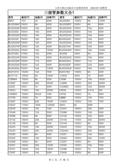
玉林万顺达电脑芯片级维修资料 2010-07-20整理玉林万顺达电脑芯片级维修资料 2010-07-20整理玉林万顺达电脑芯片级维修资料 2010-07-20整理玉林万顺达电脑芯片级维修资料 2010-07-20整理玉林万顺达电脑芯片级维修资料 2010-07-20整理玉林万顺达电脑芯片级维修资料 2010-07-20整理玉林万顺达电脑芯片级维修资料 2010-07-20整理玉林万顺达电脑芯片级维修资料 2010-07-20整理玉林万顺达电脑芯片级维修资料 2010-07-20整理玉林万顺达电脑芯片级维修资料 2010-07-20整理玉林万顺达电脑芯片级维修资料 2010-07-20整理玉林万顺达电脑芯片级维修资料 2010-07-20整理玉林万顺达电脑芯片级维修资料 2010-07-20整理玉林万顺达电脑芯片级维修资料 2010-07-20整理玉林万顺达电脑芯片级维修资料 2010-07-20整理玉林万顺达电脑芯片级维修资料 2010-07-20整理玉林万顺达电脑芯片级维修资料 2010-07-20整理玉林万顺达电脑芯片级维修资料 2010-07-20整理玉林万顺达电脑芯片级维修资料 2010-07-20整理玉林万顺达电脑芯片级维修资料 2010-07-20整理玉林万顺达电脑芯片级维修资料 2010-07-20整理玉林万顺达电脑芯片级维修资料 2010-07-20整理玉林万顺达电脑芯片级维修资料 2010-07-20整理玉林万顺达电脑芯片级维修资料 2010-07-20整理玉林万顺达电脑芯片级维修资料 2010-07-20整理玉林万顺达电脑芯片级维修资料 2010-07-20整理玉林万顺达电脑芯片级维修资料 2010-07-20整理玉林万顺达电脑芯片级维修资料 2010-07-20整理玉林万顺达电脑芯片级维修资料 2010-07-20整理玉林万顺达电脑芯片级维修资料 2010-07-20整理。
威尔士190L高级应用基础激光技术产品介绍说明书

W 190 L High Grade:Application-based Laser Tech-nology, the optimum solutionfor demanding applicationsDATASHEETD Do your customers require reli-able sensors suitable for demanding applications, using Laser Technology?WLG 190TL and WTB 190TL sen-sors are reliable, user friendly andvery accurate. The sensors havered-light laser diodes, which con-form to Protection Class 2. Theprecise visible light spot allowsfast and accurate alignment ofthe sensors even to the smallesttarget. The sensors’ fastresponse times make them idealfor most high-speed applications.Light or dark switching can beprogrammed or, if the applicationso requires, a timer function withtime delays up to 10 seconds, canbe activated. The teach-in func-tion, available at the push of a but-ton or remotely, permits simpleand highly effective sensing andrange adjustment. Menu prompt-ing is provided via the clearnumeric display. All programmingfunctions may be disabled to pre-vent unintentional adjustments.The option of a rotating M8 con-nector or 2 m cable version isavailable as standard, as is thecompact, industry-standard plastichousing which permits the use ofthe device even in harsh environ-ments.What‘s available?WTB 190TL: high resolution utilis-es CMOS technology. Ideal for thereliable detection of objects withreflective surfaces. Backgroundsuppression (BGS) or foregroundsuppression (FGS) can beprogrammed.WLG 190T: ideal for detectingtransparent objects, e.g.PET bottles.Two versions are available:for applications operating understandard conditions, e.g. foil/film,or for applications with increasedrequirements, e.g. thin-walledbottles.W 190 L High Grade, application examplesWLG 190 T (1): Edge control of transparent packaging material.Sector: Packaging industry.WTB 190 TL (2): 2-point teach-in,FGS mode, product detection, correct thickness of packs.Sector: Packaging industry.▲WTB 190TL: 2-point teach-in, FGS mode, detection of cheese slices.Sector: Food industry.▲WTB 190TL: 2-point teach-in, FGS mode, level control.Sector: Packaging industry.WTB 190TL: Position teach-in, BGS mode,checking presence.Sector: Electronic and semiconductor industry.▲WTB 190TL: 2-point teach-in, FGS mode, detection of gelatine capsules in blister packs.Sector: Pharmaceutical industry.▲▲(1)(2)▲▲WLG 190T: Transparent bottles.Sector: Bottling.▲WTB 190TL: 1-point teach-in, BGS mode, detecting or counting the IC pins.Sector: Electronics.▲WLG 190T: Detecting whether multi-part objects are assembled correctly. In this example: Is the transparent lid on the head? Sector: Packaging industry.▲WLG 190T: Ampoule syringes and breakage test.Sector: Pharmaceutical industry.WLG 190T: Detection of thin-walled glass ampoules.Sector: Pharmaceutical industry.▲W 190 L4S I C Kx x -05-2005Standard direction of the material being scanned Centre of optical axis, sender Centre of optical axis, receiver Mounting holes, Ø approx. 3.1 mm +/– button; select mode button Teach-in buttonPlug 4-pin, M8, 90°rotatable or cable 2 m, 4-wire Status indicator LED, green: Laser on Status indicator LED, yellow: output active Numerical displayL+M Q ETL+M Q ET■Laser LED, visible red light, Class 2■Scanning distance adjustment byteach-in function■Programmable background or fore-ground suppression■Programmable output: light/dark switching■Numeric display with menu prompts57894321610*)*)*) Adjustment via External Teach (ET)PNP ➞L+NPN ➞MWTB 190TL Photoelectric proximity switch, background/foreground suppression, long range, teach-inCDRHAccession Number 0 31 22 45¨S I C K 5WTB 190TL3035402025510150% o f s c a nn i n g d i s t a n c e■Operating distance ■Scanning distance,max. typical1)Object with 90% reflectance (with reference to standard white according to DIN 5033)2)Background suppression 3)Foreground suppression4)Average service life 50,000 h at T A = +25°C 5)Limit values6)Must be within V S tolerances 7)Without load12)A =V S connections reverse-polarityprotectedB =Output Q short-circuitprotected8)With resistive load9)With light/dark ratio 1:110)Do not bend below 0°C 11)Reference voltage 50 V DCDistance [mm]*)Equipment model with 5 m PVC cable or M8 plug, 3-pin on request0[mm]1002002706S I C Kx x -05-2005Standard direction of the material being scanned Centre of optical axis, sender Centre of optical axis, receiver Mounting holes, Ø approx. 3.1 mm +/– button; select mode button Teach-in buttonPlug 4-pin, M8, 90°rotatable or cable 2 m, 4-wire Status indicator LED, green: Laser on Status indicator LED, yellow: output active Numerical displayL+M Q ETL+M Q ET■Laser LED, visible red light, Class 2■Scanning distance adjustment byteach-in function■Programmable background or fore-ground suppression■Programmable output: light/dark switching■Numeric display with menu prompts57894321610*)*)*) Adjustment via External Teach (ET)PNP ➞L+NPN ➞MWTB 190TL Photoelectric proximity switch, background/foreground suppression, short range, teach-inCDRHAccession Number 0 31 22 45¨S I C K 7WTB 190TL31.522.510.5% o f s c a n n i n g d i s t a n c e(with reference to standard white according to DIN 5033)2)Background suppression 3)Foreground suppressionat T A = +25°C 5)Limit values6)Must be within V S tolerances 7)Without loadA =V S connections reverse-polarityprotectedB =Output Q short-circuitprotected9)With light/dark ratio 1:110)Do not bend below 0°C 11)Reference voltage 50 V DCDistance [mm]*)Equipment model with 5 m PVC cable or M8 plug, 3-pin on request0[mm]20406080100120■Operating distance ■Scanning distance,max. typical8S I C Kx x -05-2005WLG 190T Photoelectric reflex switch, for transparent objects, standard applications, teach-in, laserCentre of optical axisMounting holes, Ø approx. 3.1 mm +/– button; select mode buttonTeach-in buttonPlug 4-pin, M8, 90°rotatable or cable 2 m, 4-wire Status indicator LED, green: Laser on Status indicator LED, yellow: output active Numerical displayL+M Q ETL+M Q ET■Laser LED, visible red light, Class 2■Sensitivity setting by teach-in ■Precision auto-collimated optics ■Programmable output: light/dark switching■Numeric display with menu prompts57843216*)*)*) Sensitivity control via External Teach (ET)PNP ➞L+NPN ➞MCDRHAccession Number 0 31 22 45¨S I C K9WLG 190T4657123[m]100101O p e r a t i n g r e s e r v e1)Reflector P 250 F included with delivery 2)Average service life 50,000 h at T A = +25°C 3)Limit values4)Must be within V S tolerances 5)Without load6)With resistive load10)A =V S connections reverse-polarityprotectedB =Output Q short-circuitprotected7)With light/dark ratio 1:18)Do not bend below 0°C 9)Reference voltage 50 V DC0[m]1234567■Operating range■Scanning range,max. typical*)Equipment model with 5 m PVC cable or M8 plug, 3-pin on requestDistance [m]10S I C Kx x -05-2005WLG 190T Photoelectric reflex switch, for transparent objects, increased requirements, teach-in, laserMounting holes, Ø approx. 3.1 mm +/– button; select mode button Teach-in buttonPlug 4-pin, M8, 90°rotatable or cable 2 m, 4-wireCentre of optical axisStatus indicator LED, green: Laser on Status indicator LED, yellow: output active Numerical displayL+M Q ETL+M QET■Laser LED, visible red light, Class 2■Sensitivity setting by teach-in ■Precision auto-collimated optics ■Programmable output: light/dark switching■Numeric display with menu prompts57843216*)*)*) Sensitivity control via External Teach (ET)PNP ➞L+NPN ➞M¨S I C K11WLG 190T21[m]100101O p e r a t i n g r e s e r v e1)Reflector P 250 included with delivery 2)Average service life 50,000 h at T A = +25°C 3)Limit values4)Must be within V S tolerances 5)Without load6)With resistive load10)A =V S connections reverse-polarityprotectedB =Output Q short-circuitprotected7)With light/dark ratio 1:18)Do not bend below 0°C 9)Reference voltage 50 V DC0[m]0.511.52■Operating range■Scanning range,max. typical*)Equipment model with 5 m PVC cable or M8 plug, 3-pin on requestDistance [m]No TimerOn DelayStatus indicator LED, green: Laser on Status indicator LED, yellow: output active Numerical display+/– buttons; select mode buttons Teach-in buttonWTB 190TL photoelectric proximity switch, CMOS, teach-in, laserdLY Delay F-bFGS/BGS SEL Select ondON Delay oFFNo Timer oFdOFF Delay onEONE shot L dLight ON/Dark ON LonLight ON donDark ON SEnSensitivity tchTeaching type 1Pt1-point teach-in 2Pt2-point teach-in PoSPosition teach-in dSP Display onDisplay on oFFDisplay off rSt Reset noUnreset YES Reset unL UnlockFGS/Foreground suppression BGS/Background suppression On (LED yellow)On (LED green)Select-Mode buttonTeach-in buttonOffOnBlinking2 s)Background Foreground RUN ModeRUN ModeOFF Delay ONE shotTimer units/duration:3 digits = unit (ms), adjustable in 1 ms increments 1-999 ms 2 digits = unit (s), adjustable in 1 s increments 1-10 s54321Light ONDark ONDisplay ON Display OFFRUN Mode RUN ModeReset NOReset YES RUN Mode RUN ModeTeaching typeTeaching typex x -05-2005S I C K 13WTB 190TLWTB 190TL photoelectric proximity switch, CMOS, teach-in, laser14S I C K x x -05-2005When unlockWhen lock Display of switching thres-RUN ModeRUN ModeRUN ModeLock:The sensor is protected from inadvertent adjustments.Unlock:The sensor can be programmed.WTB 190TLS I C K15WTB 190TL photoelectric proximity switch, CMOS, teach-in, laserNo TimerOn DelayOffOnBlinking2 s)OFF Delay ONE shotRUN Mode RUN ModeLight ON Dark ONdLY Delay SEL Select ondON Delay oFFNo Timer oFdOFF Delay onEONE shot L dLight ON/Dark ON LonLight ON donDark ONASc/Auto sensitivity control SPdResponse time tndTresh level dSP Display onDisplay on oFFDisplay off rSt Reset noUnreset YES Reset Loc LockunL Unlock Status indicator LED, green: Laser on Status indicator LED, yellow: output active Numerical display+/– buttons; select mode buttons Teach-in buttonOn (LED yellow)On (LED green)Select-Mode buttonTeach-in button54321Timer units/duration:3 digits = unit (ms), adjustable in 1 ms increments 1-999 ms 2 digits = unit (s), adjustable in 1 s increments 1-10 sWLG 190T photoelectric reflex switch, for glass detection, teach-in, laserx x -05-2005WLG 190T photoelectric reflex switch, for glass detection, teach-in, laserx x -05-2005RUN Mode RUN ModeAuto sensitivity Auto sensitivity Reset NOReset YES NO = no reset YES = reset“YES“ selected: reset to Factory defaultSwitch levelON level OFF level Reflector level 1969210029389100When unlock When lock Display of switching thres-Lock:The sensor is protected from inadvertent adjustments.Unlock:The sensor can be programmed.WLG 190Tx x -05-2005Accessories ConnectorsContact assignment according to EN 50044Dimensional drawings and order informationø 11.6M 8x 138.4Cable diameter max. 5.0 mm423128.0116M8x112.5Cable diameter max. 5.0 mm4231SENSICK screw-in system M8, 4-pin, enclosure rating IP 67Female connector M8, 4-pin, straightTypeDOS-0804-GOrder no.6 009 974Female connector M8, 4-pin, right angleTypeDOS-0804-WOrder no.6 009 9752/wht 1/brn 4/blk3/bluø 1030.5R min 1)M 8x 13/blu626M 8x116.5ø 10R min 1)1/brn4/blk2/whtFemale connector M8, 4-pin, straightType DOL-0804-G02M DOL-0804-G05M DOL-0804-G10M Order no.6 009 8706 009 8726 010 754Cable length2 m 5 m 10 mFemale connector M8, 4-pin, right angleType DOL-0804-W02M DOL-0804-W05M DOL-0804-W10M Order no.6 009 8716 009 8736 010 755Cable length 2 m 5 m 10 m 1)Minimum bend radius in dynamic useR min = 20 x cable diameterCable diameter 5 mm, 4 x 0.25 mm 2, sheath PVCCable diameter 5 mm, 4 x 0.25 mm 2, sheath PVCx x -05-2005S I C K 2068.810204751.61061.651474.45.65Reflector, 47 x 47 mm 2Plastic design for temperatures up to 65 °C TypeP 250Order no.5 304 812 3.57.110204751.61061.651474.45.65.7Reflector, 47 x 47 mm 2micro triple, 2 hole mountingTypeP 250 FOrder no.5 308 843Dimensional drawings and order information 53.849.711.551.5152.531.3204.63.510.724Mounting bracket for W 190 L (included with delivery)TypeBEF-WK-W190Order no.5 311 362ReflectorsMounting systemsAccessories W 190 L21S I C Kx x -05-2005Contact:A u s t r a l i aPhone +61 3 9497 41001800 33 48 02 – tollfree********************.auB e l g i u m /L u x e m b o u r g Phone +32 (0)2 466 55 66******************B r a s i lPhone +55 11 5091-4900******************.br C e s k á R e p u b l i k a Phone +420 2 57 91 18 50******************C h i n aPhone +852-2763 6966******************.hk D a n m a r kPhone +45 45 82 64 00******************D e u t s c h l a n dPhone +49 (0)2 11 53 01-250******************E s p a ñaPhone +34 93 480 31 00******************F r a n c ePhone +33 1 64 62 35 00******************G r e a t B r i t a i nPhone +44 (0)1727 831121******************.uk I n d i aPhone +91 (11) 2696 7651*******************************I t a l i aPhone +39 02 27 40 93 19******************J a p a nPhone +81 (0)3 3358 1341******************K o r e aPhone +82-2 786 6321/4************************N e d e r l a n d sPhone +31 (0)30 229 25 44******************N o r g ePhone +47 67 81 50 00************************Ös t e r r e i c hPhone +43 (0)22 36 62 28 8-0********************P o l s k aPhone +48 22 837 40 50******************R e p u b l i k a S l o w e n i j a Phone +386 (0)1-47 69 990*********************R u s s i aPhone +7 95 775 05 30*****************************S c h w e i zPhone +41 41 619 29 39*********************S i n g a p o r ePhone +65 6744 3732***********************.sg S u o m iPhone +358-9-25 15 800******************S v e r i g ePhone +46 8 680 64 50******************T ür k i y ePhone +90 216 388 95 90 pbx *******************.tr T a i w a nPhone +886 2 2365-6292***********************.net U S A /C a n a d a /M éx i c o Phone +1(952) 941-67801 800-325-7425 – tollfree**********************More representatives and agencies in all major industrial nations at 8 010 553/x x -05-05 • G O /X X • P r i n t e d i n G e r m a n y (05.05) • S u b j e c t t o c h a n g e w i t h o u t p r i o r n o t i c e • T h e s p e c i f i e d p r o d u c t f e a t u r e s a n d t e c h n i c a l d a t a d o n o t r e p r e s e n t a n y g u a r a n t e e • 01 A 4-2c i n t 22SICK AG •Industrial Sensors •Waldkirch •。
TTA0001
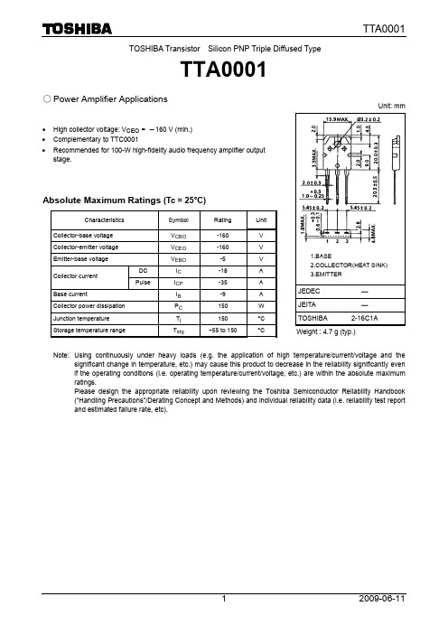
TTA0001
Unit: mm
Absolute Maximum Ratings (Tc = 25°C)
Characteristics
Symbol
Rating
Unit
Collector-base voltage Collector-emitter voltage Emitter-base voltage
• Though TOSHIBA works continually to improve Product’s quality and reliability, Product can malfunction or fail. Customers are responsible for complying with safety standards and for providing adequate designs and safeguards for their hardware, software and systems which minimize risk and avoid situations in which a malfunction or failure of Product could cause loss of human life, bodily injury or damage to property, including data loss or corruption. Before creating and producing designs and using, customers must also refer to and comply with (a) the latest versions of all relevant TOSHIBA information, including without limitation, this document, the specifications, the data sheets and application notes for Product and the precautions and conditions set forth in the “TOSHIBA Semiconductor Reliability Handbook” and (b) the instructions for the application that Product will be used with or for. Customers are solely responsible for all aspects of their own product design or applications, including but not limited to (a) determining the appropriateness of the use of this Product in such design or applications; (b) evaluating and determining the applicability of any information contained in this document, or in charts, diagrams, programs, algorithms, sample application circuits, or any other referenced documents; and (c) validating all operating parameters for such designs and applications. TOSHIBA ASSUMES NO LIABILITY FOR CUSTOMERS’ PRODUCT DESIGN OR APPLICATIONS.
上海龙整电器接近开关说明书

上海龙整电器接近开关说明书
上海龙整电器接近开关已开发为在IO链路环境中工作,在这种环境下,需要监测和记录传感性能。
由于上海龙整电器接近开关的简单和全面定制,客户可以从许多设置组合中进行选择,并满足他们的特定要求。
随着这些具有ToF技术和集成IO-Link功能的光电上海龙整电器接近开关的推出,Carlo Gavazzi通过更广泛的产品供应来加强其在市场上的地位。
具有IO链路功能的LD30激光光电上海龙整电器接近开关:IP69K不锈钢外壳或IP67塑料外壳两个独立的开关信号通道(SSC)远程背景抑制可通过电位计或IO连接在50至1000mm之间调节感应距离操作方式:单点、两点、窗口
温度报警和记录功能
逻辑门功能:AND,OR,X-OR和选通复位触发器
工作温度:-25°C至+50°C(-13°至+122°F)
延时功能:开启延迟、关闭延迟、单次前缘或后缘,值在1ms到32767分钟之间两个完全可配置的独立输出:NPN/PNP、推拉、外部输入或远程示教NO或NC 2米PVC电缆或M8插头
IO链路通信v1.1这些上海龙整电器接近开关设计用于满足工业要求,并能准确检测食品和饮料、机床、包装和包装、塑料和橡胶以及材料处理
市场中不同尺寸、形状或表面结构的物体。
MMSZ4xxxT1G系列和SZMMSZ4xxxT1G系列零点电阻电源器件的商品说明书

MMSZ4686T1G MMSZ4686T1G.MMSZ4xxxT1G Series, SZMMSZ4xxxT1G Series Zener Voltage Regulators 500 mW, Low I ZT SOD−123 Surface MountThree complete series of Zener diodes are offered in the convenient, surface mount plastic SOD−123 package. These devices provide a convenient alternative to the leadless 34−package style.Features•500 mW Rating on FR−4 or FR−5 Board•Wide Zener Reverse V oltage Range − 1.8 V to 43 V•Low Reverse Current (I ZT) − 50 m A•Package Designed for Optimal Automated Board Assembly •Small Package Size for High Density Applications•ESD Rating of Class 3 (>16 kV) per Human Body Model•SZ Prefix for Automotive and Other Applications Requiring Unique Site and Control Change Requirements; AEC−Q101 Qualified and PPAP Capable•These Devices are Pb−Free and are RoHS Compliant*Mechanical Characteristics:CASE:V oid-free, transfer-molded, thermosetting plastic case FINISH:Corrosion resistant finish, easily solderableMAXIMUM CASE TEMPERATURE FOR SOLDERING PURPOSES: 260°C for 10 SecondsPOLARITY:Cathode indicated by polarity band FLAMMABILITY RATING:UL 94 V−0MAXIMUM RATINGSRating Symbol Max Units Total Power Dissipation on FR−5 Board,(Note 1) @ T L = 75°CDerated above 75°C P D5006.7mWmW/°CThermal Resistance, (Note 2) Junction−to−Ambient R q JA340°C/WThermal Resistance, (Note 2) Junction−to−Lead R q JL150°C/WJunction and Storage Temperature Range T J, T stg−55 to+150°CStresses exceeding those listed in the Maximum Ratings table may damage the device. If any of these limits are exceeded, device functionality should not be assumed, damage may occur and reliability may be affected.1.FR−5 = 3.5 X 1.5 inches, using the minimum recommended footprint.2.Thermal Resistance measurement obtained via infrared Scan Method.*For additional information on our Pb−Free strategy and soldering details, please download the ON Semiconductor Soldering and Mounting Techniques Reference Manual, SOLDERRM/D.Cathode AnodeSee specific marking information in the device marking column of the Electrical Characteristics table on page 3 of this data sheet.DEVICE MARKING INFORMATIONSOD−123CASE 425STYLE 1Device Package Shipping†ORDERING INFORMATIONMARKING DIAGRAM†For information on tape and reel specifications, including part orientation and tape sizes, please refer to our T ape and Reel Packaging Specifications Brochure, BRD8011/D.MMSZ4xxxT1G SOD−123(Pb−Free)3,000 /Tape & ReelMMSZ4xxxT3G SOD−123(Pb−Free)10,000 /Tape & Reel xx= Device Code (Refer to page 3)M= Date CodeG= Pb−Free Package(Note: Microdot may be in either location)1SZMMSZ4xxxT1G SOD−123(Pb−Free)3,000 /Tape & ReelSZMMSZ4xxxT3G SOD−123(Pb−Free)10,000 /Tape & ReelELECTRICAL CHARACTERISTICS (T A = 25°C unless otherwise noted, V F = 0.9 V Max. @ I F = 10 mA)Symbol ParameterV Z Reverse Zener Voltage @ I ZTI ZT Reverse CurrentI R Reverse Leakage Current @ V RVR Reverse VoltageI F Forward CurrentV F Forward Voltage @ I FProduct parametric performance is indicated in the Electrical Characteristics for the listed test conditions, unless otherwise noted. Product performance may not be indicated by the Electrical Characteristics if operated under different conditions.ELECTRICAL CHARACTERISTICS (T A = 25°C unless otherwise noted, V F = 0.9 V Max. @ I F = 10 mA)Device*DeviceMarkingZener Voltage (Note 3)Leakage CurrentV Z (Volts)@ I ZT I R @ V RMin Nom Max m A m A VoltsMMSZ4678T1G CC 1.71 1.8 1.89507.51 MMSZ4679T1G CD 1.90 2.0 2.105051 MMSZ4680T1G CE 2.09 2.2 2.315041 MMSZ4681T1G CF 2.28 2.4 2.525021 MMSZ4682T1G CH 2.565 2.7 2.8355011 MMSZ4683T1G CJ 2.85 3.0 3.15500.81 MMSZ4684T1G CK 3.13 3.3 3.47507.5 1.5 MMSZ4685T1G CM 3.42 3.6 3.78507.52 MMSZ4686T1G CN 3.70 3.9 4.105052 MMSZ4687T1G CP 4.09 4.3 4.525042 SZMMSZ4687T1G CG6 4.09 4.3 4.525042 MMSZ4688T1G CT 4.47 4.7 4.9450103 MMSZ4689T1G CU 4.85 5.1 5.3650103 MMSZ4690T1G/T3G CV 5.32 5.6 5.8850104 MMSZ4691T1G CA 5.89 6.2 6.5150105 MMSZ4692T1G CX 6.46 6.87.145010 5.1 MMSZ4693T1G CY7.137.57.885010 5.7 MMSZ4694T1G CZ7.798.28.61501 6.2 MMSZ4695T1G DC8.278.79.14501 6.6 MMSZ4696T1G DD8.659.19.56501 6.9 MMSZ4697T1G DE9.501010.505017.6 MMSZ4698T1G DF10.451111.55500.058.4 MMSZ4699T1G DH11.401212.60500.059.1 MMSZ4700T1G DJ12.351313.65500.059.8 MMSZ4701T1G DK13.301414.70500.0510.6 MMSZ4702T1G DM14.251515.75500.0511.4 MMSZ4703T1G†DN15.201616.80500.0512.1 MMSZ4704T1G DP16.151717.85500.0512.9 MMSZ4705T1G DT17.101818.90500.0513.6 MMSZ4706T1G DU18.051919.95500.0514.4 MMSZ4707T1G DV19.002021.00500.0115.2 MMSZ4708T1G DA20.902223.10500.0116.7 MMSZ4709T1G DX22.802425.20500.0118.2 MMSZ4710T1G DY23.752526.25500.0119.0 MMSZ4711T1G†EA25.652728.35500.0120.4 MMSZ4712T1G EC26.602829.40500.0121.2 MMSZ4713T1G ED28.503031.50500.0122.8 MMSZ4714T1G EE31.353334.65500.0125.0 MMSZ4715T1G EF34.203637.80500.0127.3 MMSZ4716T1G EH37.053940.95500.0129.6 MMSZ4717T1G EJ40.854345.15500.0132.6 3.Nominal Zener voltage is measured with the device junction in thermal equilibrium at T L = 30°C ±1°C.*Include SZ-prefix devices where applicable.†MMSZ4703 and MMSZ4711 Not Available in 10,000/Tape & ReelTYPICAL CHARACTERISTICSV Z , T E M P E R A T U R E C O E F F I C I E N T (m V /C )°θV Z , NOMINAL ZENER VOLTAGE (V)Figure 1. Temperature Coefficients (Temperature Range −55°C to +150°C)V Z , T E M P E R A T U R E C O E F F I C I E N T (m V /C )°θ100101V Z , NOMINAL ZENER VOLTAGE (V)Figure 2. Temperature Coefficients (Temperature Range −55°C to +150°C)1.21.00.80.60.40.20T, TEMPERATURE (5C)Figure 3. Steady State Power Derating P p k, P E A K S U R G E P O W E R (W A T T S )PW, PULSE WIDTH (ms)Figure 4. Maximum Nonrepetitive Surge PowerP D , P O W E R D I S S I P A T I O N (W A T T S )V Z , NOMINAL ZENER VOLTAGEFigure 5. Effect of Zener Voltage onZener ImpedanceZ Z T , D Y N A M I C I M P E D A N C E ()ΩTYPICAL CHARACTERISTICSC , C A P A C I T A N C E (p F )V Z , NOMINAL ZENER VOLTAGE (V)Figure 6. Typical Capacitance 1000100101V Z , ZENER VOLTAGE (V)1001010.10.01I Z , Z EN E R C U R R E N T (m A )V Z , ZENER VOLTAGE (V)1001010.10.01I R , L E A K A G E C U R R E N T (A )μV Z , NOMINAL ZENER VOLTAGE (V)Figure 7. Typical Leakage Current10001001010.10.010.0010.00010.00001I Z , Z E N E R C U R R E N T (m A )Figure 8. Zener Voltage versus Zener Current(V Z Up to 12 V)Figure 9. Zener Voltage versus Zener Current(12 V to 91 V)SOD−123CASE 425−04ISSUE GDATE 07 OCT 2009SCALE 5:1NOTES:1.DIMENSIONING AND TOLERANCING PER ANSIY14.5M, 1982.2.CONTROLLING DIMENSION: INCH.DIM MIN NOM MAXMILLIMETERSINCHESA0.94 1.17 1.350.037A10.000.050.100.000b0.510.610.710.020c1.600.150.055D 1.40 1.80E 2.54 2.69 2.840.100---3.680.140L0.253.860.0100.0460.0020.0240.0630.1060.1450.0530.0040.0280.0710.1120.152MIN NOM MAX3.56H E---------0.006------------GENERICMARKING DIAGRAM**For additional information on our Pb−Free strategy and solderingdetails, please download the ON Semiconductor Soldering andMounting Techniques Reference Manual, SOLDERRM/D.SOLDERING FOOTPRINT**This information is generic. Please refer to device datasheet for actual part marking. Pb−Free indicator, “G” ormicrodot “ G”, may or may not be present.XXX= Specific Device CodeM= Date CodeG= Pb−Free Package1STYLE 1:PIN 1. CATHODE2. ANODE0.910.036ǒmminchesǓSCALE 10:1------q001010°°°°(Note: Microdot may be in either location) MECHANICAL CASE OUTLINEPACKAGE DIMENSIONSON Semiconductor and are trademarks of Semiconductor Components Industries, LLC dba ON Semiconductor or its subsidiaries in the United States and/or other countries.ON Semiconductor reserves the right to make changes without further notice to any products herein. ON Semiconductor makes no warranty, representation or guarantee regarding the suitability of its products for any particular purpose, nor does ON Semiconductor assume any liability arising out of the application or use of any product or circuit, and specifically disclaims any and all liability, including without limitation special, consequential or incidental damages. ON Semiconductor does not convey any license under its patent rights nor theON Semiconductor and are trademarks of Semiconductor Components Industries, LLC dba ON Semiconductor or its subsidiaries in the United States and/or other countries.ON Semiconductor owns the rights to a number of patents, trademarks, copyrights, trade secrets, and other intellectual property. A listing of ON Semiconductor’s product/patent coverage may be accessed at ON Semiconductor makes no warranty, representation or guarantee regarding the suitability of its products for any particular purpose, nor does ON Semiconductor assume any liability arising out of the application or use of any product or circuit, and specifically disclaims any and all liability, including without limitation special, consequential or incidental damages.PUBLICATION ORDERING INFORMATIONTECHNICAL SUPPORTNorth American Technical Support:Voice Mail: 1 800−282−9855 Toll Free USA/Canada Phone: 011 421 33 790 2910LITERATURE FULFILLMENT :Email Requests to:*******************ON Semiconductor Website: Europe, Middle East and Africa Technical Support:Phone: 00421 33 790 2910For additional information, please contact your local Sales RepresentativeMMSZ4686T1G MMSZ4686T1G.。
VCO190-2950TY资料
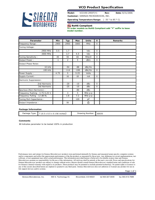
VCO Product SpecificationModel:VCO190-2950T(Y) Rev:Date:8/31/2006Customer:SIRENZA MICRODEVICES, INC.Operating Temperature Range:(-35 ° to 85 ° C)RoHS CompliantTo order models as RoHS Compliant add "Y" suffix to basemodel number.Parameter Min Typ Max Units X RemarksFrequency Range - 290029503000MHz XTuning Voltage:2900 MHz 0.5 1.7Vdc X3000 MHz 3.7 4.5Vdc XTuning Sensitivity - 455565MHz/V XOutput Power - -125dBm XOutput Phase Noise:10 kHz -94-88dBc/Hz100 kHz -114-108dBc/Hz XPower Supply - 4.755 5.25VoltsSupply Current - 1618mA XHarmonic Suppression:2nd Harmonic -20-10dBc X3rd Harmonic -25-10dBc XSpurious (Non-Harmonic) - -80dBcFrequency Pushing - 4.75-5.25 V 35MHz p-pFrequency Pulling - 12 dB RL 1.87.2MHz p-pTuning Port Capacitance - 120pFOutput Impedance - 50Package InformationPackage Type: T(0.5 x 0.5 x 0.156 inches)Drawing Number: 60035CommentsX Indicates parameter to be tested 100% in productionPerformance tests and ratings for Sirenza Microdevices'products were performed internally by Sirenza and measured using specific computer systems and/or components and reflect the approximate performance of the the products as measured by those tests.Any difference in circuit implementation,test software,or test equipment may affect actual performance.The information provided herein is believed to be reliable at press time and Sirenza Microdevices assumes no responsibility for the use of this information.All such use shall be entirely at the user's own risk.Prices and specifications for Sirenza Microdevices'products are subject to change without notice.Buyers should consult Sirenza Microdevices'standard terms and conditions of sale for Sirenza's limited warranty with regard to its products.These products may be patented or include patented technology.No patent rights or licenses to any of the circuits described herein are implied or granted to any third party.Sirenza Microdevices does not authorize or warrant any product for use in life-support devices and/or systems.Sirenza Microdevices,Inc.。
X9C102系列数字电位器

DESCRIPTIONThe Xicor X9C102/103/104/503 is a solid state nonvola-tile potentiometer and is ideal for digitally controlledresistance trimming.The X9C102/103/104/503 is a resistor array composed of 99 resistive elements. Between each element and at either end are tap points accessible to the wiper element.The position of the wiper element is controlled by the CS ,U/D , and INC inputs. The position of the wiper can be stored in nonvolatile memory and then be recalled upon a subsequent power-up operation.The resolution of the X9C102/103/104/503 is equal to the maximum resistance value divided by 99. As an example, for the X9C503 (50K Ω) each tap point repre-sents 505Ω.All Xicor nonvolatile memories are designed and tested for applications requiring extended endurance and data retention.FEATURES•Compatible with X9102/103/104/503•Low Power CMOS —V CC = 5V—Active Current, 3mA Max —Standby Current, 500µA Max •99 Resistive Elements—Temperature Compensated—± 20% End to End Resistance Range •100 Wiper Tap Points—Wiper Positioned via Three-Wire Interface —Similar to TTL Up/Down Counter —Wiper Position Stored in Nonvolatile Memory and Recalled on Power-Up•100 Year Wiper Position Data Retention •X9C102 = 1K Ω•X9C103 = 10K Ω•X9C503 = 50K Ω•X9C104 = 100K ΩE 2POT ™ Nonvolatile Digital PotentiometerX9C102/103/104/503E 2POT ™ is a trademark of Xicor, Inc.3863 FHD F01FUNCTIONAL DIAGRAML WHVX9C102/103/104/503PIN DESCRIPTIONSV H and V LThe high (V H) and low (V L) terminals of the X9C102/103/ 104/503 are equivalent to the fixed terminals of a mechanical potentiometer. The minimum voltage is –5V and the maximum is +5V. It should be noted that the terminology of V L and V H references the relative position of the terminal in relation to wiper movement direction selected by the U/D input and not the voltage potential on the terminal.V WV W is the wiper terminal, equivalent to the movable terminal of a mechanical potentiometer. The position of the wiper within the array is determined by the control inputs. The wiper terminal series resistance is typically 40Ω.Up/Down (U/D)The U/D input controls the direction of the wiper movement and whether the counter is incremented or decremented.Increment (INC)The INC input is negative-edge triggered. Toggling INC will move the wiper and either increment or decrement the counter in the direction indicated by the logic level on the U/D input.Chip Select (CS)The device is selected when the CS input is LOW. The current counter value is stored in nonvolatile memory when CS is returned HIGH while the INC input is also HIGH. After the store operation is complete the X9C102/ 103/104/503 will be placed in the low power standby mode until the device is selected once again.PIN CONFIGURATIONPIN NAMESSymbol DescriptionV H High TerminalV W Wiper TerminalV L Low TerminalV SS GroundV CC Supply VoltageU/D Up/Down InputINC Increment InputCS Chip Select InputNC No Connect3863 PGM T01V CCCSV LV W3863 FHD F02.2INCU/DV HV SS12348765X9C102/103/104/503DIP/SOICX9C102/103/104/503DEVICE OPERATIONThere are three sections of the X9C102/103/104/503: the input control, counter and decode section; the non-volatile memory; and the resistor array. The input control section operates just like an up/down counter. The output of this counter is decoded to turn on a single electronic switch connecting a point on the resistor array to the wiper output. Under the proper conditions the contents of the counter can be stored in nonvolatile memory and retained for future use. The resistor array is comprised of 99 individual resistors connected in series. At either end of the array and between each resistor is an electronic switch that transfers the potential at that point to the wiper.The INC, U/D and CS inputs control the movement of the wiper along the resistor array. With CS set LOW the X9C102/103/104/503 is selected and enabled to respond to the U/D and INC inputs. HIGH to LOW transitions on INC will increment or decrement (depending on the state of the U/D input) a seven-bit counter. The output of this counter is decoded to select one of one-hundred wiper positions along the resistive array.The wiper, when at either fixed terminal, acts like its mechanical equivalent and does not move beyond the last position. That is, the counter does not wrap around when clocked to either extreme.The value of the counter is stored in nonvolatile memory whenever CS transistions HIGH while the INC input is also HIGH.When the X9C102/103/104/503 is powered-down, the last counter position stored will be maintained in the nonvolatile memory. When power is restored, the con-tents of the memory are recalled and the counter is reset to the value last stored.OPERATION NOTESThe system may select the X9C102/103/104/503, move the wiper, and deselect the device without having to store the latest wiper, position in nonvolatile memory. The wiper movement is performed as described above; once the new position is reached, the system would the keep INC LOW while taking CS HIGH. The new wiper position would be maintained until changed by the system or until a power-down/up cycle recalled the previously stored data.This would allow the system to always power-up to a preset value stored in nonvolatile memory; then during system operation minor adjustments could be made. The adjustments might be based on user preference: system parameter changes due to temperature drift, etc...The state of U/D may be changed while CS remains LOW. This allows the host system to enable the X9C102/103/104/503 and then move the wiper up and down until the proper trim is attained.T IW/R TOTALThe electronic switches on the X9C102/103/104/503 operate in a “make before break” mode when the wiper changes tap positions. If the wiper is moved several positions, multiple taps are connected to the wiper for t IW (INC to V W change). The R TOTAL value for the device can temporarily be reduced by a significant amount if the wiper is moved several positions.R TOTAL with V CC RemovedThe end to end resistance of the array will fluctuate once V CC is removed.SYMBOL TABLEX9C102/103/104/503ABSOLUTE MAXIMUM RATINGS*Temperature under Bias..................–65°C to +135°C Storage Temperature.......................–65°C to +150°C Voltage on CS, INC, U/D and V CCwith Respect to V SS...............................–1V to +7V Voltage on V H and V LReferenced to V SS.................................–8V to +8V ∆V = |V H–V L|X9C102 (4V)X9C103, X9C503, and X9C104 (10V)Lead Temperature (Soldering, 10 seconds)....+300°C Wiper Current.....................................................±1mA *COMMENTStresses above those listed under “Absolute Maximum Ratings” may cause permanent damage to the device. This is a stress rating only and the functional operation of the device at these or any other conditions above those listed in the operational sections of this specifica-tion is not implied. Exposure to absolute maximum rating conditions for extended periods may affect device reliability.ANALOG CHARACTERISTICSElectrical CharacteristicsEnd-to-End Resistance Tolerance (20)Power Rating at 25°CX9C102.......................................................16mW X9C103, X9C503, and X9C104..................10mW Wiper Current............................................±1mA Max. Typical Wiper Resistance.........................40Ω at 1mA Typical Noise..........................< –120dB/Hz Ref: 1VResolution Resistance.............................................................1%LinearityAbsolute Linearity(1)........................................±1.0 Ml(2) Relative Linearity(3).....................................±0.2 Ml(2)Temperature Coefficient(–40°C to +85°C)X9C102......................................+600 ppm/°C Typical X9C103, X9C503, X9C104........+300 ppm/°C Typical Ratiometric Temperature Coefficient............±20 ppm Wiper AdjustabilityUnlimited Wiper Adjustment (Non-Store operation) Wiper Position Store Operations...................10,000 Data Changes Physical CharacteristicsMarking IncludesManufacturer‘s TrademarkResistance Value or CodeDate CodeTest Circuit #1Test Circuit #2Notes:(1)Absolute Linearity is utilized to determine actual wiper voltage versus expected voltage= (V w(n)(actual) – V w(n)(expected)) = ±1 Ml Maximum.(2) 1 Ml = Minimum Increment = R TOT/99.(3)Relative Linearity is a measure of the error in step size between taps = V W(n+1) – [V w(n) + Ml] = +0.2 Ml.X9C102/103/104/503 RECOMMENDED OPERATING CONDITIONSTemperature Min.Max. Commercial0°C+70°C Industrial–40°C+85°C Military–55°C+125°C3863 PGM T03.1Supply Voltage Limits X9C102/103/104/5035V ±10%D.C. OPERATING CHARACTERISTICS (Over recommended operating conditions unless otherwise specified.)LimitsSymbol Parameter Min.Typ.(4)Max.Units Test ConditionsI CC V CC Active Current13mA CS = V IL, U/D = V IL or V IH andINC = 0.4V to 2.4V @ max. t CYCI SB Standby Supply Current200500µA CS = V CC – 0.3V, U/D and INC =V SS or V CC – 0.3VI LI CS, INC, U/D Input±10µA V IN = V SS to V CCLeakage CurrentV IH CS, INC, U/D Input2V CC + 1VHIGH VoltageV IL CS, INC, U/D Input–10.8VLOW VoltageR W Wiper Resistence40100ΩMax. Wiper Current ±1mAV H VH Terminal Voltage–5+5VV L VL Terminal Voltage–5+5VC IN(5)CS, INC, U/D Input10pF V CC = 5V, V IN = V SS,Capacitance T A = 25°C, f = 1MHz3863 PGM T05.3 STANDARD PARTSPart Number Maximum Resistance Wiper Increments Minimum Resistance X9C1021KΩ10.1Ω40ΩX9C10310KΩ101Ω40ΩX9C50350KΩ505Ω40ΩX9C104100KΩ1010Ω40Ω3863 PGM T08.1 Notes:(4)Typical values are for T A = 25°C and nominal supply voltage.(5)This parameter is periodically sampled and not 100% tested.3863 PGM T04.2X9C102/103/104/503MODE SELECTIONA.C. CONDITIONS OF TESTNotes:(6)Typical values are for T A = 25°C and nominal supply voltage.(7)This parameter is periodically sampled and not 100% tested.(8)MI in the A.C. timing diagram refers to the minimum incremental change in the V W output due to a change in the wiper position.X9C102/103/104/503Typical Frequency Response for X9C102TEST CONDITIONS V CC = 5VTemp. = 25°C Wiper @ Tap 50V H = 0.5V RMSNormalized (0dB @ 1KHz)Test Circuit #1TEST CONDITIONS V CC = 5VTemp. = 25°C Wiper @ Tap 50V H = 2V RMS Test Circuit #1Typical Total Harmonic Distortion for X9C102N O R M A L I Z E D G A I N (d B )9630–3–6–9–12–15–18–210.010.101.0010.00100.001000.0010000.00FREQUENCY IN KHzT H D (%)2.01.81.61.41.21.00.80.60.40.20.00.010.101.0010.00100.001000.0010000.00FREQUENCY IN KHz3863 FHD F063863 FHD F07X9C102/103/104/503Typical Linearity for X9C102Typical Frequency Response for X9C103TEST CONDITIONS V CC = 5VTemp. = 25°C Wiper @ Tap 50V H = 0.5V RMSNormalized (0dB @ 1KHz)Test Circuit #1N O R M A L I Z E D G A I N (d B )9630–3–6–9–12–15–18–210.010.101.0010.00100.001000.00FREQUENCY IN KHz3863 FHD F09X9C102/103/104/503Typical Total Harmonic Distortion for X9C103Typical Linearity for X9C103TEST CONDITIONS V CC = 5VTemp. = 25°C Wiper @ Tap 50V H = 2V RMS Test Circuit #1T H D (%)2.01.81.61.41.21.00.80.60.40.20.00.010.101.0010.00100.001000.00FREQUENCY IN KHz3863 FHD F10X9C102/103/104/503Typical Frequency Response for X9C503Typical Total Harmonic Distortion for X9C503TEST CONDITIONS V CC = 5VTemp. = 25°C Wiper @ Tap 50V H = 2V RMS Test Circuit #1TEST CONDITIONS V CC = 5VTemp. = 25°C Wiper @ Tap 50V H = 0.5V RMSNormalized (0dB @ 1 KHz)Test Circuit #19630-3-6-9-12-15-18-210.010.101.0010.00100.00FREQUENCY IN KHzN O R M A L I Z E D G A I N (d B )1000.0091.81.61.41.21.00.80.60.40.20.00.010.101.0010.00100.00FREQUENCY IN KHzT H D (%)1000.003863 FHD F123863 FHD F13X9C102/103/104/503Typical Linearity for X9C503Typical Frequency Response for X9C104TEST CONDITIONS V CC = 5VTemp. = 25°C Wiper @ Tap 50V H = 0.5V RMSNormalized (0dB @ 1 KHz)Test Circuit #19630-3-6-9-12-15-18-210.010.101.0010.00100.001000.00FREQUENCY IN KHzN O R M A L I Z E D G A I N (d B )3863 FHD F15X9C102/103/104/503Typical Total Harmonic Distortion for X9C104Typical Linearity for X9C104TEST CONDITIONS V CC = 5VTemp. = 25°C Wiper @ Tap 50V H = 2V RMS Test Circuit #12.01.81.61.41.21.00.80.60.40.20.00.010.101.0010.00100.0010000.00FREQUENCY IN KHzT H D (%)1000.003863 FHD F16X9C102/103/104/5033926 FHD F01TYP NOTE: ALL DIMENSIONS IN INCHES (IN PARENTHESES IN MILLIMETERS)MAX.PACKAGING INFORMATION8-LEAD PLASTIC DUAL IN-LINE PACKAGE TYPE PNOTE: ALL DIMENSIONS IN INCHES (IN PARENTHESES IN MILLIMETERS)X9C102/103/104/503PACKAGING INFORMATION8-LEAD PLASTIC SMALL OUTLINE GULL WING PACKAGE TYPE SNOTE: ALL DIMENSIONS IN INCHES (IN PARENTHESIS IN MILLIMETERS)3926 FHD F22X9C102/103/104/503ORDERING INFORMATIONX9CXXX X XTemperature RangeBlank = Commercial = 0°C to +70°CI = Industrial = –40°C to +85°CM = Military = –55°C to +125°CPackageP = 8-Lead Plastic DIPS = 8-Lead SOICEnd to End Resistance102 = 1KΩ103 = 10KΩ503 = 50KΩ104 = 100KΩLIMITED WARRANTYDevices sold by Xicor, Inc. are covered by the warranty and patent indemnification provisions appearing in its Terms of Sale only. Xicor, Inc. makes no warranty, express, statutory, implied, or by description regarding the information set forth herein or regarding the freedom of the described devices from patent infringement. Xicor, Inc. makes no warranty of merchantability or fitness for any purpose. Xicor, Inc. reserves the right to discontinue production and change specifications and prices at any time and without notice.Xicor, Inc. assumes no responsibility for the use of any circuitry other than circuitry embodied in a Xicor, Inc. product. No other circuits, patents, licenses are implied.U.S. PATENTSXicor products are covered by one or more of the following U.S. Patents: 4,263,664; 4,274,012; 4,300,212; 4,314,265; 4,326,134; 4,393,481; 4,404,475;4,450,402; 4,486,769; 4,488,060; 4,520,461; 4,533,846; 4,599,706; 4,617,652; 4,668,932; 4,752,912; 4,829, 482; 4,874, 967; 4,883, 976. Foreign patents and additional patents pending.LIFE RELATED POLICYIn situations where semiconductor component failure may endanger life, system designers using this product should design the system with appropriate error detection and correction, redundancy and back-up features to prevent such an occurence.Xicor's products are not authorized for use in critical components in life support devices or systems.1.Life support devices or systems are devices or systems which, (a) are intended for surgical implant into the body, or (b) support or sustain life, and whosefailure to perform, when properly used in accordance with instructions for use provided in the labeling, can be reasonably expected to result in a significant injury to the user.2.A critical component is any component of a life support device or system whose failure to perform can be reasonably expected to cause the failure of the lifesupport device or system, or to affect its safety or effectiveness.。
LTST-C190TGKT
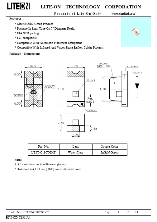
Min. Typ. Max. Unit Test Condition
Luminous Intensity
IV
C190TGKT 71.0 150.0
mcd
IF = 20mA Note 1
Viewing Angle
2θ1/2 C190TGKT
130
deg Note 2 (Fig.6)
Peak Emission Wavelength
Property of Lite-On Only
Typical Electrical / Optical Characteristics Curves (25 °C Ambient Temperature Unless Otherwise Noted)
Part No. : LTST-C190TGKT BNS-OD-C131/A4
Source Color InGaN Green
Part No. : LTST-C190TGKT BNS-OD-C131/A4
Page : 1 of 11
洸子其科技是一家从事发光管产品的研发、生产和销售公司,致 力于为国内国际市场提供高质量,低成本的各类 LED 发光二极管。
主营的产品有:SMD LED 发光二极管 色彩有:红、橙、黄、绿、 蓝、白、紫、粉红、单色双色及三色,封装有:0402、0603、0802、 0805、1204、1206、3528、5050、3020、3014、2835、3535、335、 020、正面发光及侧面发光等…
2. θ1/2 is the off-axis angle at which the luminous intensity is half the axial luminous intensity. 3. The dominant wavelength, λd is derived from the CIE chromaticity diagram and represents the
190产品说明书
目录产品特点 (1)工作环境 (1)技术参数 (1)产品介绍 (2)主机前面板 (2)主机后面板 (2)带铝基板LED老化台 (3)带铝基板LED老化台 (4)操作说明 (6)基本配置 (14)产品特点:恒流驱动每颗LED,单个LED之间不受影响,每台老化台相对独立,通过一台老化主机可以同时老化多种形状,大小和不同时间需求的LED。
老化系统具有强大的功能,五组可调节电流,带温度测试和频率输出功能,通过设定老化时间和脉冲冲击时间。
工作环境:工作电压:220V±10%工作温度:23℃±2℃相对湿度:10%-90%系统参数电流输出:0.5-1000mA功率:0-10W12电流分辨率:0.1mA电流精度:0.5-100mA :0.5±1%100mA-1000mA :±1%输出频率:1-3000Hz占空比:1:99-99:1定时时间:1000小时产品介绍:老化主机前面板介绍:(图一)1:左下方第一到第五组老化台的电流输出调节旋钮2:左上方为液晶显示界面,傍边分别是电源指示灯和运行指示灯3:键盘操作界面包括“电流”键、“温度”键、“频率”键、“时间”键、“*”键、“#”键和数字键。
各按键功能简介:(1)“电流”键:切换到电流显示界面;(2)“温度”键:切换到温度测量界面;(3)“频率”键:切换到频率输出界面;(4)“时间”键:切换到冲击测试界面;(5)“*”键和“#”键功能根据具体操作界面而不同,详见主机操作说明;(6)数字键:设置修改各项参数;4:右下方航空插头为温度探测器接口;5:右边红色开关为主机电源开关。
3老化主机后面板介绍(图二)1:主机电源插口2:第一组老化台电源输出口3:第二组老化台电源输出口4:第三组老化台电源输出口5:第四组老化台电源输出口6:第五组老化台电源输出口带铝基板的大功率老化台:(图三)4(图三)1:操作手柄(用来压紧或放松电源触点)2:正极定位销(调整电源触点与LED正极接触)3:负极定位销(调整电源触点与LED负极接触)4:正极触点(与LED的正极接触)5:负极触点(与LED的负极接触)6:转换器(老化带铝基板的LED不需要用转换器,转换器的位置调到与夹具持平)7:固定夹具8:负载输出线9:散热器不带铝基板的老化台(图四)5图四1:操作手柄(用来压紧或放松电源触点)2:正极定位销(调整电源触点与LED正极接触)3:负极定位销(调整电源触点与LED负极接触)4:正极触点(与LED的正极接触)5:负极触点(与LED的负极接触)6:转换器(转换器的位置调高)7:绝缘块(用来固定LED)8:负载输出线9:散热器67操作说明一、测试主机功能操作说明:测试前请先检查与老化台连线是否正常。
西安威克产品介绍

先进的安全技术,防爆,防火,防漏。
内置电容器芯体故障保护使故障安全隔离 特殊的工艺工程及优质环保灌注材料。
多重保护
无油,无蜡,全干式结构。 壳体采用钢板喷塑结构。
油或蜡,容易漏出。
马口铁外壳结构,容易生锈。 内置一般放电电阻。
内置放电 内置超低损耗放电电阻。
随变张力卷制
提高电容器元件端面的平整 度 。确保每只产品,都能通 过严格的过电流试验,确保 质量的稳定性.
优越的产品工艺
德威克电容器
边缘加厚 金属化薄膜镀层边缘加厚提高电容器 元件过电流的能力 。 大大增加喷金面的有效面积。 随变张力 渐进方阻 过电流试验 每只产品,都要通过严格的过电流试验, 确保质量的稳定性. 真空灌注 采用在高真空抽取元件内的水份,并注 入性能良好环保树脂。 有效提高自愈合的能力和综合电气性 能。
自愈合能力
金属化薄膜的电极采用锌铝复合 技术 击穿点使电极介质层气化分开, 产生绝缘区,电容器恢复正常工 作能力。
DWKCL滤波电抗器
概述: 德威克滤波电抗器用于电力系统低压无功补偿,与电容器串联,能有效抑制 电网谐波,改善系统的电压波形,提高系统的功率因数。 电抗器结构: 电抗器为铁芯干式结构,产品分为单相和三相。 产品型号: DWKCLS□-○/△
只有每年2000次的投切次数。 介质损耗大于0.25/Kvar。。 60000小时的寿命设计甚至更低。
极低的介质损耗,只有0.25/Kvar。。
低温升
100000小时的寿命设计。
先进的安全保护性能
德威克电容器
自愈合 三防结构 自愈合能力,自我修复,容降低
其它厂家电容器
联动保护装置
有自愈合能力,但容降大。 安全技术不过关,有可能爆裂, 起火。 油或蜡的灌注材料,容易起火。
常用三极管参数大全

玉林万顺达电脑芯片级维修资料 2010-07-20整理玉林万顺达电脑芯片级维修资料 2010-07-20整理玉林万顺达电脑芯片级维修资料 2010-07-20整理玉林万顺达电脑芯片级维修资料 2010-07-20整理玉林万顺达电脑芯片级维修资料 2010-07-20整理玉林万顺达电脑芯片级维修资料 2010-07-20整理玉林万顺达电脑芯片级维修资料 2010-07-20整理玉林万顺达电脑芯片级维修资料 2010-07-20整理玉林万顺达电脑芯片级维修资料 2010-07-20整理玉林万顺达电脑芯片级维修资料 2010-07-20整理玉林万顺达电脑芯片级维修资料 2010-07-20整理玉林万顺达电脑芯片级维修资料 2010-07-20整理玉林万顺达电脑芯片级维修资料 2010-07-20整理玉林万顺达电脑芯片级维修资料 2010-07-20整理玉林万顺达电脑芯片级维修资料 2010-07-20整理玉林万顺达电脑芯片级维修资料 2010-07-20整理玉林万顺达电脑芯片级维修资料 2010-07-20整理玉林万顺达电脑芯片级维修资料 2010-07-20整理玉林万顺达电脑芯片级维修资料 2010-07-20整理玉林万顺达电脑芯片级维修资料 2010-07-20整理玉林万顺达电脑芯片级维修资料 2010-07-20整理玉林万顺达电脑芯片级维修资料 2010-07-20整理玉林万顺达电脑芯片级维修资料 2010-07-20整理玉林万顺达电脑芯片级维修资料 2010-07-20整理玉林万顺达电脑芯片级维修资料 2010-07-20整理玉林万顺达电脑芯片级维修资料 2010-07-20整理玉林万顺达电脑芯片级维修资料 2010-07-20整理玉林万顺达电脑芯片级维修资料 2010-07-20整理玉林万顺达电脑芯片级维修资料 2010-07-20整理玉林万顺达电脑芯片级维修资料 2010-07-20整理。
UCC28950中文版技术文档资料
UCC28950中⽂版技术⽂档资料TEXAS INSTRUMENTSUCC28950—具有同步整流功能的环保型相移全桥控制器产品特点●增强型宽域谐振的零点电压开关(ZVS)能⼒●直接控制同步整流(SR)●轻载效率管理包括-猝发模式操作-不连续导电模式(DCM),可编程阈值实现动态SR开/关控制-可编程的⾃适应延时—可编程斜坡补偿可实现平均电流或峰值电流控制和电压模式控制●具备使功能控制及闭环软启动功能●可以双向同时实现编程开关频率到1MHz.●(+/-3%)逐个周期限流保护并有打嗝模式保护●150µA启动电流●V DD ⽋压锁定●温度范围-400C—1250C应⽤领域▲相移全桥变换器▲服务器与电信电源▲⼯业电源系统▲⾼密度电源架构,▲太阳能逆变器,电动车产品简介UCC28950相移控制器是在TEXAS公司的UCCx895系列相移控制器⼯业标准基础上对功能进⾏优化提⾼⽽推出的新产品,可以为当今⾼性能要求的电源系统提供最⾼的转换效率。
UCC28950应⽤了先进的全桥控制和主动的同步整流输出控制,初级信号允许编程延迟来确保在宽负载电流和输⼊电压范围内ZVS能正常运⾏,⽽负载电流⾃然地调整次级同步整流器开关延迟时间,最终实现效率达到最⼤。
UCC28950同样也具有多样的轻载管理特性包括猝发模式和动态SR开/关控制,以确保ZVS 操作向下延伸到更轻的负载。
另外,UCC28950⽀持峰值电流控制及电压控制模式,编程开关频率可达1MHz. 保护⽅式多样化,包括逐个周期限流,UVLO(⽋压锁定)和热保护关闭。
90度相移插⼊同步运⾏⼯作可以轻易在使⽤UCC28950的两电源转换器间实现。
UCC28950(采⽤TSSOP-24封装)订购信息绝对最⼤额定值⼯作环境中空⽓的温度范围(除⾮另有说明)⑴⑵⑴超过上表中标有“绝对最⼤额定值”时,设备可能会被永久性破坏。
⑵这些器件对静电敏感,遵循正确的设备处理程序。
⑶所有的电压都是与地线有关的,除⾮另有说明。
CB1 系列控制与保护开关电器(常规型)型号说明说明书

整定电流范围代号R1R2R3R4S1S2TUV额定工作电流Ie(A)123263125160整定电流Ir1范围(A)0.15~0.60.35~1.4 1.25~53~12 4.5~188~3232~6363~125125~160400V 电动机功率范围 Pe(kW)0.06~0.120.18~0.370.55~1.52.2~5.53~7.55.5~1518.5~3037~5575短路分断能力 Ics(kA/400V)50150基本保 护功能E 型控制器 短路、过载(EF 时只报警不脱扣)、断相(EF 时只报警不脱扣)、接地、瞬时大电流(短路短延时)Z 型控制器 短路、过载(ZF 时只报警不脱扣)、瞬时大电流(短路短延时)CB1系列控制与保护开关电(常规型)型号说明控制器类别产品辅助触头配置情况标配情况增选说明ZA 附加辅助触头输出功能的智能控制器辅助:3NO3NC 就绪:1NO (1)故障:1NO1NC (2)可选T024或T230,辅助变为3NO2NCZL 附加负载指示功能的智能控制器辅助:1NO1NC 就绪:1NO (1)故障:1NO1NC (2)/ZM 附加通信功能的智能控制器ZP 附加过载预报警和报警输出功能的智能控制器辅助:1NO1NC 就绪:1NO (1)故障:1NO1NC (2) 过载报警:2NO2NC 可选F21,过载报警变为1NO ZF 附加过载报警不脱扣功能的智能控制器EJ无附加功能的电子型控制器辅助:1NO1NC可选F22ES 附加就绪、故障信号输出的电子型控制器辅助:1NO1NC 就绪:1NO 故障:1NO1NC可选F22或F21+G10或F21+T024或F21+T230EF附加过载报警不脱扣功能的电子型控制器辅助:1NO1NC 过载报警:1NO可选F21或F21+B11注:(1)CB1-125时无,若需要请另外注明 (2)CB1-125时为一组带公共点的转换触头 (3)CB1-125无电子型控制器额定工作电流Ie(A): 12、32、63、125、160CB132ZAS2选配功能选配附件Z 型控制器可选功能断相保护不平衡保护接地故障保护工艺欠流保护堵转保护起动超时保护热过载预报警功能附件代号备注FKM1可逆模块,适用于控制器为ZA、ZF、ZL、ZP、EJ、EF、ES的CB1-12、CB1-32FKM1/TM 可逆模块,适用于控制器为ZM 的CB1-12、CB1-32F212NO1NC 辅助触点,EF、ZF、ZP、ES(同时选配G10或T024或T230时)可选F222NO2NC 辅助触点,EJ、ES 可选B111NO1NC 故障触点,EF 可选G101NO 过载报警触点,ES(需同时选配F21)可选T024DC24V 远程脱扣,ES (需同时选配F21)、ZA 可选T230AC230V 远程脱扣,ES (需同时选配F21)、ZA 可选CB1系列控制与保护开关电器(派生型)型号说明及选型举例电机控制方案设计符号适用规格选型举例双速控制CB1-12CB1-32CB1-63CB1-125CB1-160CB1-32/EFS2/DESS1注:高速消防型、低速基本型三速控制CB1-12CB1-32CB1-63CB1-125CB1-160CB1-63/EFT/D3ESS2/ESR4注:高速消防型,中、低速基本型星三角控制(外接)CB1-32CB1-63CB1-125CB1-160CB1-125/ZAU/J星三角控制(内接)CB1-125CB1-160CB1-125/ZAU/J2可逆控制CB1-12CB1-32CB1-63CB1-125CB1-160CB1-63/EST/N55kWM~~M30kW~M11kW/4kW注:(1)双速、三速控制时为高速控制器及电流范围代号; (2)中速、低速控制器及电流范围代号定义参照高速;(3)派生类型J 适用于32、63、125A、160A,派生类型J2适用于125A、160A。
950用户手册
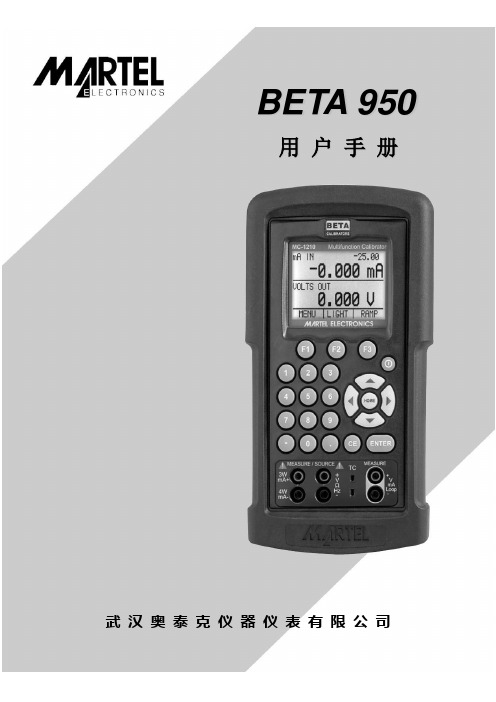
B E T A950用户手册武汉奥泰克仪器仪表有限公司1、产品简介BETA950是一种便携式、由电池供电的多功能过程校验仪,该设备可测量或模拟输出多种电信号和物理量。
BETA950具有如下功能及特点:1、具有双通道显示,显示屏上半部分的显示区域可显示电压、电流和压力的测量值,显示屏下半部分的显示区域可显示电压、电流、压力、热电阻、热电偶、频率和电阻的测量值,还可以模拟输出脉冲值。
2、热电偶输入输出端带有自动冷端温度补偿。
3、每个电信号或物理量的测量量程范围内均可设定5个递增或递减数值点。
4、互动式的使用菜单。
5、可使用自带的RS232接口进行远程控制。
6、独立的重复读数功能可校验变送器。
7、可进行开关测试。
1.1标准配置一套完整的BETA950应包括如下部分:BETA950主机,使用手册,测量导线套,橡胶外壳,NIST 证书。
1.2 安全事项请在使用BETA950时需注意以下几点:1、请勿超过额定电压,详见量程范围说明。
2、遵循一切设备安全条例。
3、当测量导线插在电流测量端时,请不要使测量头接触电压源。
4、如BETA950已损坏,请不要继续使用。
5、在使用前请检查仪器的外壳,查看是否有裂纹或缺口。
6、要特别注意连接导线的接头部位的绝缘材料是否完整。
7、测量时请选择正确的功能和量程。
8、使用前请确认电池仓的盖子是否已关严。
9、打开电池仓之前请将测量导线从BETA950上拔下。
10、检查测量导线的绝缘材料是否已经损坏或已有金属部分裸露在外,在使用BETA950前请将已坏的测量导线进行更换。
11、在使用测量导线的夹头时,手指部分请不要触摸夹头。
12、请勿非正常使用BETA950,这种行为可能会减少仪器的使用寿命。
13、在使用中如有疑问,请与我公司技术售后服务部门联系。
14、请不要在含有爆炸性气体、蒸汽或灰尘的环境中使用BETA950。
15、当外接压力模块时,请确保压力导管在连接或拆除时处于关闭和泄压状态。
产品目录介绍

厂内规范
厚度(μm) film Thickness
密度 density (g/cm3)
抗拉强度
MD
tensile strength
(MPa)
TD
断裂伸长率
MD
Elongation
(%)
TD
尺寸稳定性
MD
Dimensional
Stability (%)
TD
熔点Melting point
PP EVA
软化点Softening Point
厂内规范
1.051 59 48
110.00 100.00
2
-1
厂内规范 ASTMD 882-3 ASTMD 882-3
ASTMD 1204-78
260.00 125.00 85.00 105.00
ASTMD E 794-85
ASTMD E 794-85 23℃,60/70%RH
23.00
38℃,90%RH
160℃ 180℃ 180℃
预压时间 5~15s 10s 10s 15s 10s
成型时间 70~120s 100~180s
70s 120s 120s
TAT50-cfc阻胶离型膜规格书
项目 Item
规格 Specification
结果 Result 标准 Test Method
外观 Appearance
成型时间 70~120s 100~180s
70s 120s 120s
TAP90-cle阻胶离型膜规格书
项目 Item
规格 Specification 结果 Result 标准 Test Method
外观 Appearance
平整,颜色一致,无明显缺陷及 异物 。
- 1、下载文档前请自行甄别文档内容的完整性,平台不提供额外的编辑、内容补充、找答案等附加服务。
- 2、"仅部分预览"的文档,不可在线预览部分如存在完整性等问题,可反馈申请退款(可完整预览的文档不适用该条件!)。
- 3、如文档侵犯您的权益,请联系客服反馈,我们会尽快为您处理(人工客服工作时间:9:00-18:30)。
VCO Product Specification
Model:VCO190-950T(Y) Rev:Date:8/31/2006
Customer:SIRENZA MICRODEVICES, INC.
Operating Temperature Range:(-35 ° to 85 ° C)
RoHS Compliant
To order models as RoHS Compliant add "Y" suffix to base
model number.
Parameter Min Typ Max Units X Remarks
Frequency Range - 8409501060MHz X
Tuning Voltage:
840 MHz 1 1.5Vdc X
1060 MHz 8.510Vdc X
Tuning Sensitivity - 203050MHz/V X
Output Power - -303dBm X
Output Phase Noise:
10 kHz -106-100dBc/Hz
100 kHz -126-120dBc/Hz X
Power Supply - 11.751212.25Volts
Supply Current - 3040mA X
Harmonic Suppression:
2nd Harmonic -15-10dBc X
3rd Harmonic -20-10dBc X
Spurious (Non-Harmonic) - -90dBc
Frequency Pushing - 11.75-
14MHz p-p
12.25 V
Frequency Pulling - 12 dB RL 1.22MHz p-p
Tuning Port Capacitance - 50pF
Output Impedance - 50
Package Information
Package Type: T(0.5 x 0.5 x 0.156 inches)Drawing Number: 60035
Comments
X Indicates parameter to be tested 100% in production
Performance tests and ratings for Sirenza Microdevices'products were performed internally by Sirenza and measured using specific computer systems and/or components and reflect the approximate performance of the the products as measured by those tests.Any difference in circuit implementation,test software,or test equipment may affect actual performance.The information provided herein is believed to be reliable at press time and Sirenza Microdevices assumes no responsibility for the use of this information.All such use shall be entirely at the user's own risk.Prices and specifications for Sirenza Microdevices'products are subject to change without notice.Buyers should consult Sirenza Microdevices'standard terms and conditions of sale for Sirenza's limited warranty with regard to its products.These products may be patented or include patented technology.No patent rights or licenses to any of the circuits described herein are implied or granted to any third party.Sirenza Microdevices does not authorize or warrant any product for use in life-support devices and/or systems.
Sirenza Microdevices,Inc.。