MC9S08GW64 Single-phase single-chip energy meter
Freescale Semiconductor MC9S08QG8应用说明书

Freescale Semiconductor Application Note AN3048Rev. 1.00, 11/2005Table of Contents1Introduction The MC9S08QG8 is a small pin-count, yet feature rich, microcontroller. The properties of this MCU make it ideal for an application such as a stand-alone inter-integrated circuit (IIC) analog-to-digital converter (ADC). This document demonstrates how the MC9S08QG8 can be used as a stand-alone ADC accessed by the IIC. In this demonstration application, commands sent via IIC will select different ADC channels and set a threshold limit to be used for an alarm indicator. 1.1RequirementsTo run this demo, you need:•Two DEMO9S08QG8 demo boards•DEMO9S08QG8 Quick Start Guide (comes with demo board)•MC9S08QG8 data sheet from .•IIC driver code used in this document — available as AN3048SW.zip from .•True-Time Simulator CW3.1 with MC9S08QG8 patchUsing IIC to Read ADC Values on MC9S08QG8by Donnie GarciaApplication EngineeringMicrocontroller Division1Introduction. . . . . . . . . . . . . . . . . . . . . . . . . . . . . . 11.1Requirements . . . . . . . . . . . . . . . . . . . . . . . . 11.2IIC Features. . . . . . . . . . . . . . . . . . . . . . . . . . 21.3Implementing IIC Communication . . . . . . . . . 21.3.1Master and Slave Initialization . . . . . . . 31.4Defining the Messaging Strategy. . . . . . . . . . 31.4.1Master-to-Slave Communication . . . . . 31.4.2Slave-to-Master Communication . . . . . 32Demonstrating the Stand-Alone ADC Application. 42.1Slave Board. . . . . . . . . . . . . . . . . . . . . . . . . . 42.2Master Board. . . . . . . . . . . . . . . . . . . . . . . . . 42.3Connecting the Demo Boards . . . . . . . . . . . . 52.4Starting the Demonstration . . . . . . . . . . . . . . 53Conclusion . . . . . . . . . . . . . . . . . . . . . . . . . . . . . .6Introduction1.2IIC FeaturesThe IIC communications protocol is a standard that can be used to interface an MCU with other devices such as temperature sensors, EEPROMS, LCDs, other MCUs, and A/D or D/A devices. This protocol makes it easy to add additional devices onto an existing IIC bus because each device contains a unique slave address. All devices on the IIC bus monitor activity, but slaves only respond to messages that are addressed to them. IIC communication is accomplished through a simple two-line interface. Data is relayed through the SDA pin, and the clock is supplied by the master on the SCL pin.The MC9S08QG8 contains the standard IIC module that is in the HCS08 Family of microcontrollers. The features of this module include:•Compatibility with the IIC bus standards•Multi-master operation•Flexible baud rate generator•Interrupt-driven byte-by-byte transferThe interrupt capabilities of this peripheral provide a very important feature that allows interrupts to occur at address match, arbitration loss, and data transfers. All of these features together allow IIC communication to be handled by an interrupt service routine (ISR) that can be used for both master and slave operation.NOTEFor additional information on IIC module initialization, functionality, andregisters and control and status bits, please see the IIC chapter of theMC9S08QG8 data sheet (available from ).1.3Implementing IIC CommunicationThe IIC chapter of the MC9S08QG8 data sheet provides an “IIC Module Quick Start” figure and “Typical IIC Interrupt Routine” flow chart. These detail the most straight-forward method to implement IIC communications. Because the application described in this document uses that method, please have the IIC chapter of the MC9S08QG8 data sheet near for reference.The IIC master and slave code examples for this demonstration (AN3048SW.zip) use the documented method to create the interrupt service routine (ISR) for IIC. For example, the first decision in the “Typical IIC Interrupt Routine” flow chart is whether the device is set as a master or slave. This is accomplished in the example ISR with the code:if (IICC_MST){...} else {...}This checks the status of the MST bit in the IIC control register:•If it is set (MST = 1), the code will proceed to execute what is defined inside the curly brackets,i.e., master mode operation will be handled.•If MST is not set (MST = 0), code will execute the else statement, i.e., slave mode operation will be handled.It is important to note that not all decisions that are defined in this flow chart can be made by the status and control bits that are provided in the IIC registers. For example, when in master mode, you must know when the second-to-last byte and the last byte to be read are received. This is accomplished in the exampleIntroduction ISR by a variable, num_to_rec , which defines the number of bytes to receive. This variable is used to compare against a count variable that keeps track of the amount of data that has passed from slave tomaster. So in the example code provided, you will see that variables are used along with status and control bits to achieve the routine depicted in the IIC chapter of the MC9S08QG8 data sheet.1.3.1Master and Slave InitializationBoth master and slave can use the same ISR routine as shown in the demo code, but there is a difference in the initialization and startup sequence between these two. See the “IIC Module Quick Start” figure in the IIC chapter of the MC9S08QG8 data sheet for complete initialization sequence.As soon as the slave device is initialized, it is ready to receive IIC data. A master device must initiate communication by setting up a master transmit or a master receive. This is done in the addressing sequence because the LSB of the address is the R/W bit. So, to initiate IIC communication, the address along with the R/W bit must be written to the IIC data register by the master device.1.4Defining the Messaging StrategyThe goal of this application is to get an analog reading from a MC9S08QG8 MCU via IIC communication. The master MCU will be allowed to select the ADC channel and set a threshold value that can be used to compare against. A very important step in accomplishing this is defining the messages that will be sent and received. For this application, the following messaging strategy was used.1.4.1Master-to-Slave CommunicationTable 1 shows the messages that will pass from master to slave. All possible values are shown in the data range.1.4.2Slave-to-Master CommunicationTable 2 shows all data that will pass from slave to master. Not shown here is the address that must first pass from master to slave; all IIC communication is initiated by the master.Table 1. Master-to-Slave CommunicationByteAddress (upper 7bits) R/W(1bit)Threshold Threshold Channel Select 1234Data RangeAddress (0xFE–0x00), R/W (0x1–0x0)0x03–0x000xFF–0x000x01–0x00Description Concatenation of addressand read/write Upper byte of a 10-bit threshold Lower byte of a 10-bit threshold A/D channel to be readTable 2. Slave-to-Master CommunicationByteResult Result Alarm 123Data Range0x03-0x000xFF-0x000x01-0x00Description Upper byte of a 10-bitresult Lower byte of a 10-bit result Status of the compare to the thresholdDemonstrating the Stand-Alone ADC ApplicationWith the messaging strategy defined, software development is as simple as parsing the data that is received by the master or slave. The ISR that has been created is pre-configured to create receive arrays with the data. Both slave and master contain a receive data array that can be examined while the IIC bus is inactive. It is important to wait for the IIC bus to be inactive to ensure a valid data reading. The arrays allow easy access to the messages that have been received, and C code is used to look at individual bytes in the receive data array. For example, the Alarm byte is examined with the following code:This code accesses the Alarm byte in the receive data array using an “if”statement. The same method can be used on the other bytes in the receive array so that the application code can complete the necessary tasks.2Demonstrating the Stand-Alone ADCApplicationTo demonstrate this application, you will need to connect and configure the two MC9S08QG8 demo boards. Designate one of the boards to be the master board, and the other as the slave board.2.1Slave BoardProgram the slave code (QG_IIC_Slave.c) into the slave board. Follow the directions for programming the demo board provided by the quick start guide included with the demo board. This should guide you step-by-step through opening a project, connecting through USB, and programming a demo board. This board must be powered externally, so after you have programmed it, connect an external power supply (9V, nominally) to the power connector.2.2Master BoardThe master code should be programmed into the master board. To visualize our demonstration, we will use the True-Time Simulator interface and a visualization tool. So, after the board is programmed, we will be using the debug environment.The master board must be modified to contain pullup resistors on the SDA and SCL pins. The IIC driver code in AN3048SW.zip uses PTB6 and PTB7 as the IIC pins. This is configured in software by setting the IICPS bit in SOPT2. This is a useful feature of the MC9S08QG8 that allows the IIC pins to be switched from PTA2/PTA3 to PTB6/PTB7. For IIC communication to operate, you must connect pullups on the PTB6 and PTB7 pins.Demonstrating the Stand-Alone ADC Application 2.3Connecting the Demo BoardsAfter the pullups have been added to the PTB6 and PTB7 pins on the master board, three connections must be made, as shown in Figure 1:•PTB6, PTB7, and GND must be connected between the two boards.•GND must be connected; connect GND from J1 pin 3 to J1 pin 3 of the slave board.•PTB7 and PTB6 are J1 pins 8 and 10, respectively; connect them as shown in Figure 1.Figure 1. Connecting the Two MC9S08QG8 Demo Boards2.4Starting the Demonstration1.Turn on the slave board by moving the PWR_SEL jumpers to the VDD side.2.Press the green run arrow in the True-Time Simulator to begin the master code (see Figure 2).In the visualization tool, the LED shows the status of the ALARM indicator; the graph is a visual representation of the ADC data. You can switch between channel 1 and channel 0 by pressing the SW1 (channel 0) or SW2 (channel 1) on the master demo board:—When channel 0 is selected, the potentiometer of the slave board is being read.V ary the potentiometer to see the result on the graphical representation (Figure 2) change.—When channel 1 is selected, the photo sensor is being read.Cover the photo sensor to see the graphical representation (Figure 2) change.Master BoardSlave Board •Programmed with slave code (QG_IIC_Slave)•Must be powered externally •Uses PTB6 and PTB7 as IIC pins •Remove jumpers on LED1 and LED2•Programmed with master code (QG_IIC_Master)•Add pullup resistors on SDA and SCL pins, PTB6 and PTB7, respectively •Remove jumpers on LED1 and LED2Conclusion Figure 2. Visualization Tool in True-Time Simulator & Real-Time Debugger3ConclusionThis document and provided application code (AN3048SW.zip) demonstrate how the MC9S08QG8 is well suited for an IIC application. The provided IIC driver code and application example can be used to accelerate understanding of IIC and development time.Green ArrowConclusionHow to Reach Us: Home Page:E-mail:*********************USA/Europe or Locations Not Listed:Freescale SemiconductorTechnical Information Center, CH3701300 N. Alma School RoadChandler, Arizona 85224+1-800-521-6274 or +1-480-768-2130*********************Europe, Middle East, and Africa:Freescale Halbleiter Deutschland GmbHTechnical Information CenterSchatzbogen 781829 Muenchen, Germany+44 1296 380 456 (English)+46 8 52200080 (English)+49 89 92103 559 (German)+33 1 69 35 48 48 (French)*********************Japan:Freescale Semiconductor Japan Ltd.HeadquartersARCO Tower 15F1-8-1, Shimo-Meguro, Meguro-ku,Tokyo 153-0064Japan0120 191014 or +81 3 5437 9125***************************Asia/Pacific:Freescale Semiconductor Hong Kong Ltd.Technical Information Center2 Dai King StreetTai Po Industrial EstateTai Po, N.T., Hong Kong+800 2666 8080**************************For Literature Requests Only:Freescale Semiconductor Literature Distribution Center P.O. Box 5405Denver, Colorado 802171-800-441-2447 or 303-675-2140Fax: 303-675-2150*********************************************Information in this document is provided solely to enable system and software implementers to use Freescale Semiconductor products. There are no express or implied copyright licenses granted hereunder to design or fabricate any integrated circuits or integrated circuits based on the information in this document.Freescale Semiconductor reserves the right to make changes without further notice to any products herein. Freescale Semiconductor makes no warranty, representation or guarantee regarding the suitability of its products for any particular purpose, nor does Freescale Semiconductor assume any liability arising out of the application or use of any product or circuit, and specifically disclaims any and all liability, including without limitation consequential or incidental damages. “Typical” parameters that may be provided in Freescale Semiconductor data sheets and/or specifications can and do vary in different applications and actual performance may vary over time. All operating parameters, including “Typicals”, must be validated for each customer application by customer’s technical experts. Freescale Semiconductor does not convey any license under its patent rights nor the rights of others. Freescale Semiconductor products are not designed, intended, or authorized for use as components in systems intended for surgical implant into the body, or other applications intended to support or sustain life, or for any other application in which the failure of the Freescale Semiconductor product could create a situation where personal injury or death may occur. Should Buyer purchase or use Freescale Semiconductor products for any such unintended or unauthorized application, Buyer shall indemnify and hold Freescale Semiconductor and its officers, employees, subsidiaries, affiliates, and distributors harmless against all claims, costs, damages, and expenses, and reasonable attorney fees arising out of, directly or indirectly, any claim of personal injury or death associated with such unintended or unauthorized use, even if such claim alleges that Freescale Semiconductor was negligent regarding the design or manufacture of the part. Freescale™ and the Freescale logo are trademarks of Freescale Semiconductor, Inc. All other product or service names are the property of their respective owners.© Freescale Semiconductor, Inc. 2005. All rights reserved.。
MC9RS08KA8微控制器单元说明书

Target Applications • High-brightness LED • Lighting systems control • Toys• Small handheld devices• Space-constrained applications • Small appliances• AC line voltage monitoring • Battery charger • ASIC replacement OverviewThe MC9RS08KA8 microcontroller unit (MCU) is an extremely cost-effective and highly integrated, device intended for home appliances, health care equipment and as a general-purpose microcontroller. This device is composed of standard on-chip modules including a very small and highly efficient RS08 CPU core, 254 bytes RAM, 8K bytes flash, two 8-bit modulo timers,12-channel 10-bit ADC, 2-channel 16-bit timer/PWM, inter-integrated circuit bus module, keyboard interrupt and analog comparator. The device is available in 16- and 20-pin packages.Cost-Effective Development toolsFor more information on development tools, please refer to the Freescale Development Tool Selector Guide (SG1011).CodeWarrior ® Development Studio for Microcontrollers 6.1Complimentary*CodeWarrior Development Studio for Microcontrollers is an integrated tool suite that supports software development for Freescale’s 8-bit or 32-bit microcontrollers. Designers can further accelerate application development with the help of the Processor Expert™ tool, which is an award-winning rapid application development tool in the CodeWarrior tool suite.DEMO9RS08KA8$50 MSRPCost-effective demonstration board with potentiometer, LEDs and a built-in USB-BDM cable for debugging and programming.8-bit MicrocontrollersMC9RS08KA8/4Package OptionsPart NumberPackageTemp. Range* Subject to license agreement and registrationFreescale and the Freescale logo are trademarks or registered trademarks of Freescale Semiconductor, Inc. in the U.S. and other countries. All other product or service names are the property of their respective owners. © Freescale Semiconductor, Inc. 2008.Document Number: MC9RS08KA8/4FSREV 1。
全球主流8位MCU芯片详细解剖No.1-飞思卡尔 MC9S08AC60
全球主流8 位MCU 芯片详细解剖No.1:飞思卡尔
MC9S08AC60
相信很多人在学习MCU(单片机)的时候,都是从最基本的8 位MCU 开始的。
如今,尽管32 位MCU 甚至更多功能强大的MCU 大有下探取代之势,但是在许多工程师的记忆里以及相当一部分应用领域,8 位单片机依然是不可磨灭的一代经典!本文将结合单片机的生产厂商,带你深入了解主流8 位单片机的功能结构,引脚说明,模块分析以及具体应用等等。
飞思卡尔MC9S08AC60
简介
MC9S08AC60 系列MCU 是低成本、高性能HCS08 系列8 位微处理器单元(MCU)的成员。
这个系列的单片机均由一对引脚兼容的8 位和32 位器件组成,是Flexis 系列器件的第3 个系列产品。
Flexis 系列控制器是飞思卡尔控制器联合体的连接点,使8 位与32 位兼容性成为现实。
模块结构图
系统时钟图
引脚图
通用引脚连接
重要引脚说明
电源(VDD,VSS,VDDAD,VSSAD)。
1飞思卡尔8位单片机MC9S08JM60开发板实践教程-60页word资料

第一章搭建实验环境1、实验电路板及下载器实物图片2、实验电路图本实验图包含两大部分,分别是CPU.SCH和实验资源.SCH。
CPU采用飞思卡尔8位单片机MC9S08JM60CLD,(电路图介绍)图1-3实验资源部分电路图1-4LCD串口1602液晶电路图1-5RS232接口电路图1-6数码管显示电路图1-7发光管、ad转换以及按键电路图1-83、集成开发软件环境的建立1〉运行文件CW_MCU_V6_3_SE.EXE,在电脑C盘安装飞思卡尔8位(及简化32位)单片机集成开发环境codewarrior6.3版本2〉运行USBDM_4_7_0i_Win,这个程序会在c盘的程序文件夹下增加一个目录C:\Program Files\pgo\USBDM 4.7.0,在这个目录下a>C:\Program Files\pgo\USBDM 4.7.0\FlashImages\JMxx下的文件USBDM_JMxxCLD_V4.sx是下载器的固件文件;b>C:\Program Files\pgo\USBDM4.7.0\USBDM_Drivers\Drivers下有下载器的usb驱动.因此在插入usb下载器,电脑提示发现新的usb硬件的时候,选择手动指定驱动安装位置到以上目录即可。
3〉运行USBDM_4_7_0i_Win之后,还会在目录:C:\Program Files\Freescale\CodeWarrior for Microcontrollers V6.3\prog\gdi下增加一些文件,从修改时间上来看,增加了6个文件,这些文件是为了在codewarrior集成开发环境下对usb下载器的调试、下载的支持。
4、C语言编程基础第二章 LED闪烁程序编写过程1、新建工程运行单片机集成开发环境codewarrior IDE出现如下界面●Create New Project :创建一个新项目工程●Load Example Project :加载一个示例工程●Load Previous Project :加载以前创建过的工程●Run Getting started Tutorial:运行CodeWarrior软件帮助文档●Start Using CodeWarrior:立刻使用CodeWarrior点击Create New project按钮,以创建一个新的工程,出现选择CPU的界面如下,请选择HCS08/HCS08JM Family/MC9S08JM60,在右边的Connection窗口可以选择最后一个开源下载器HCS08 Open Source BDM。
MC9S08GBGT_Low_Power_Modes_AN2493_Chinese
低功耗模式的使用
注意常量SPMSC2st2不仅设置PPDACK位以清除PPDF标记,还将PDC和PPDC位设置为逻辑1。
这是因为它们都是一次性写入位。
如果在一次写操作中未能将这些位设置为逻辑1,那么下一个STOP (停止)指令会进入停止3模式,而不是停止2。
当然,如果需要,用户可以在这条指令中选择开启停止1或停止3,而不是停止2。
与停止1相同,POR会令系统总线时钟由内部4-MHz时钟驱动,停止恢复过程相当快,从而允许代码迅速执行以恢复寄存器设置。
稳压器恢复完全调节状态的延迟与停止1相同,大概是V DD =3 V时为50µs ,V DD = 2 V时为80µs。
停止3
停止3模式不能提供最低的I DD电流,但它功能多,而且在所有停止模式中影响最小。
只要SPMSC2的PDC位设置为0,即可进入停止3。
此外还应注意,如果在停止模式下启动了LVD,或进入背景调试模式时也启动了LVD(BDCSCR中的ENBDM位已经设定为1),则此时唯一能够进入的停止模式是停止3。
当ENBDM位设置为1后执行停止指令,背景调试逻辑的系统时钟仍然有效,因此仍能继续背景调试通信。
如果用户需要能够轻松退出的停止模式,可以采用停止3。
使用内部时钟或FLL时,停止恢复时间通
特殊低功耗模式下的I DD典型值
特殊低功耗模式下的I DD典型值
特殊低功耗模式下的I DD典型值
特殊低功耗模式下的I DD典型值
特殊低功耗模式下的I DD典型值
AN2493
Rev. 2, 11/2004
General Business Information。
MC9S08QG4芯片烧写说明文档

MC9S08QG4芯片烧写说明文档芯片烧写器材PC机;周立功SmartPRO X8编程器套件(含编程器、USB线缆、电源线及软件光盘);DIP 8-pin封装MC9S08QG4型号freescale单片机,文件名为Project.abs.s19的程序文件。
烧写步骤1、安装编程器软件SmartPRO Programmer将软件安装光盘放入光驱,如图1所示,在光盘目录下找到名为“SmartPRO_Programmer图1图2_Setup”的安装文件。
双击打开安装文件后出现如图2所示对话框,单击“Next〉”进入下一步。
在如图3所示语言选择中选择“Chinese—简体中文”,单击“Next〉”进入下一步。
图3在如图4所示用于选择编程器模式的对话框中不改动默认设置,直接单击“Next〉”进图4入下一步。
在如图5所示对话框中根据实际情况选择软件安装的目标地址。
完成后单击“Next〉”图5进行软件安装。
安装完成后单击“Finish”关闭安装程序,但不要立即取出光盘,还需安装驱动程序。
2、硬件连接及驱动安装将编程器电源连接至220V插座,用USB数据线连接PC机与编程器。
打开电源,编程图6器面板上的绿灯若长亮则表示编程器工作正常。
Windows将提示安装驱动程序。
在如图6所示对话框中选择“否,暂时不(T)”,单击“下一步(N)>”进入下一步。
图7在图7所示对话框中选中“自动安装软件(推荐)(I)”,单击“下一步(N)>”。
图8在图8对话框中选中“在这些位置上搜索最佳驱动程序(S)”及“搜索可移动媒体(软盘、CD-ROM…)(M)”,单击“下一步(N)>”。
在如图9所示硬件安装向导对话框中不改变默认设置,单击“下一步(N)>”开始进图9行驱动安装。
在驱动安装时会弹出如图10所示对话框,单击“仍然继续(C)”。
图10出现如图11所示对话框时单击“浏览”,在“<光驱盘符>:\UsbDriver\PromTec\WinXP”目录下找到名为PromTec.sys的系统文件,单击“确定”完成驱动程序安装。
MC9S08QG8数据手册(中文)

MC9S08QG8数据手册苏州大学飞思卡尔嵌入式系统研发中心翻译2009年11月MC9S08QG8/4特点8位HCS08中央处理单元(CPU)—————————————————————▪20-MHzHCS08CPU(中央处理器)▪增加了BGND指令的HC08指令集▪背景调试系统▪断点能力,允许在线调试时设置单个断点(片上调试模块可多设置2个断点)▪调试模块包括2个比较器、9种触发模式。
8个深度FIFO调试模块用于存储change-of-flow地址和event-only数据。
支持标签和强制断点▪支持多达32个中断/复位源存储器选项—————————————————————▪FLASH可在全工作电压和温度下读/编程/擦除▪MC9S08QG8-8K字节FLASH,512字节RAM MC9S08QG4-4K字节FLASH,256字节RAM节能状态—————————————————————▪一种等待状态及三种停止状态时钟源选项—————————————————————▪ICS—内部时钟源模块包括由内部或外部参考控制的锁频环(FLL);内部参考的精确调整允许整个温度和电压环境下有0.2%的分辨率和2%的偏差;支持1MHz到10MHz的总线频率▪XOSC—低电压振荡器模块带有可软件选择的晶体或者陶瓷谐振器,谐振器的频率范围为从31.25kHz到38.4kHz或者从1MHz到16MHz,并且支持高达20Mhz的外部时钟源系统保护—————————————————————▪看门狗的计算机正确运行(COP)复位可选择从专用的1kHz内部时钟源或总线时钟运行▪具有复位或中断的低电压检测▪具有复位的非法操作码检测▪具有复位的非法地址检测▪FLASH块保护外围设备—————————————————————▪ADC—8通道、10位模数转换模块,还具有自动比较功能,异步时钟源,温度传感器和内部能带隙参考源通道;ADC使用实时中断计数器来硬件触发▪ACMP—具有与内部参考源比较选项的模拟比较器模块;输出可选择连接到TPM模块▪SCI—具有13位中止能力选项的串行通讯接口模块▪SPI—串行外围接口模块▪IIC—内部集成电路总线模块▪TPM—2通道定时器/脉宽调制器;每通道能用于输入捕获,输出比较,缓冲边沿对齐PWM或者缓冲中心对齐PWM▪MTIM—带预置值的8位定时器模块▪KBI—8管脚的键盘中断模块,带有软件可选择的边沿极性和边沿/电平模式输入/输出—————————————————————▪12个通用输入/输出管脚,1个仅为输入管脚和1个仅为输出管脚;每个管脚输出10mA,每片最大输出60mA▪当用作输入时端口可软件选择上拉▪当用作输出时端口可软件选择转换率和驱动强度▪RESET和IQR管脚有内部上拉以减少用户系统费用开发支持—————————————————————▪单线的背景调试接口▪片上、在线仿真器(ICE),具有实时总线捕获功能封装选项—————————————————————▪24管脚QFN封装▪16管脚PDIP封装—仅针对MC9S08QG8▪16管脚QFN封装▪16管脚TSSOP封装▪8管脚DFN封装▪8管脚PDIP封装—仅针对MC9S08QG4▪8管脚SOIC封装修改历史为了提供最新的更新信息,互联网上文档的修订版本是最新的。
MC9S08AC16数据手册(中文)

3.1 简介..................................................................................................................................................... 21 3.2 特征..................................................................................................................................................... 21 3.3 运行模式............................................................................................................................................. 21 3.4 背景调试模式 ..................................................................................................................................... 21 3.5 等待模式............................................................................................................................................. 22 3.6 停止模式............................................................................................................................................. 22
MC9RS08KA4_8中文数据手册
3FFE
3FFF
BC(JMP 机器码)
跳转地址高字节
跳转地址低字节
飞 3.4 激活背景调试模式 背景调试功能是由 RS08 核内的 BDC 管理的。在软件开发过程中,BDC 提供了
H 一种分析 MCU 操作方法。 C 有 4 种激活背景调试的方法:
*在 POR 期间或发出背景调试强制复位命令之后,拉 BKGD/MS 引脚为低
3
北京飞锐泰克科技有限公司 tel:010-59831537 fax:010-59831536
MEMORY存储芯片NAND08GW3B2CN6E中文规格书

SYNCHRONOUS RESET (FCh)When the synchronous interface is active, the SYNCHRONOUS RESET (FCh) commandis used to put a target into a known condition and to abort command sequences in pro-gress. This command is accepted by all die (LUNs), even when they are BUSY.When FCh is written to the command register, the target goes busy for t RST. Duringt RST, the selected target (CE#) discontinues all array operations on all die (LUNs). Allpending single- and multi-plane operations are cancelled. If this command is issuedwhile a PROGRAM or ERASE operation is occurring on one or more die (LUNs), the datamay be partially programmed or erased and is invalid. The command register is clearedand ready for the next command. The data register and cache register contents are inva-lid and the synchronous interface remains active.During or after t RST, the host can poll each LUN's status register.SYNCHRONOUS RESET is only accepted while the synchronous interface is active. Itsuse is prohibited when the asynchronous interface is active.Figure 42: SYNCHRONOUS RESET (FCh) Operation Array Cycle typeDQ[7:0]R/B#Electrical SpecificationsStresses greater than those listed can cause permanent damage to the device. This is astress rating only, and functional operation of the device at these or any other condi-tions above those indicated in the operational sections of this specification is not guar-anteed. Exposure to absolute maximum rating conditions for extended periods can af-fect reliability.Table 29: Absolute Maximum Ratings by DeviceNote: 1.Voltage on any pin relative to V SS.Table 30: Recommended Operating ConditionsTable 31: Valid Blocks per LUNNote: 1.Invalid blocks are blocks that contain one or more bad bits beyond ECC. The device maycontain bad blocks upon shipment. Additional bad blocks may develop over time; how-ever, the total number of available blocks will not drop below NVB during the endur-ance life of the device. Do not erase or program blocks marked invalid from the factory.Table 10: Feature Address 01h: Timing ModeNotes: 1.Asynchronous timing mode 0 is the default, power-on value.2.If the synchronous interface is active, a RESET (FFh) command will change the timing mode and data interface bits of feature address 01h to their default values. If the asyn-chronous interface is active, a RESET (FFh) command will not change the values of the timing mode or data interface bits to their default valued.32Gb, 64Gb, 128Gb, 256Gb Asynchronous/Synchronous NAND Configuration Operations。
飞思卡尔MCU时钟模块配置

飞思卡尔(FREESCALE)低功耗模式下微控制器时钟配置应用在微控制器的低功耗应用中,对时钟的设置是很重要的一个方面。
不同类型的微控制器在低功耗模式下对时钟的配置也各有不同。
飞思卡尔公司推出的增强型8位微控制器HCS08系列具有很强的低功耗性能。
其中,HCS08系列里的MC9S08QG8在同类产品的基础上对低功耗应用下的时钟又有了进一步的改进。
1 MC9S08QG8及其内部时钟模块介绍微控制器MC9S08QG8是飞思卡尔公司新推出的一款8位增强型微控制器。
它是小封装、低功耗的产品,但这并不意味着它是“低端”的产品;相反,它是一个高度集成的、功能丰富的、适用于各种应用的低价位单片机。
MC9S08QG8采用高性能、低功耗的HCS08内核,具有很高的集成度,还包括更长的电池寿命(即使工作电压低至1.8V,也能发挥最大效能)、业界领先的Flash技术以及创新的开发支持。
MC9S08QG8集成了背景调试系统(BDM)以及可进行实时总线捕捉的内置在线仿真(ICE)功能,具有单线的调试及仿真接口。
MC9S08QG8微控制器的运行模式有很多种,包括正常运行模式、等待模式、背景调试模式以及停止模式。
其中,与低功耗应用关系密切的停止模式又分为3个阶段:停止模式l——内部电路全部断电,以最大限度地节省电源;停止模式2——可选择部分断电,RAM内容保持;停止模式3——内部电路都可快速恢复运行,RAM、Flash内容保持。
MC9S08QG8内部时钟模块由4个子模块组成:锁频环、内部参考时钟、外部振荡器、时钟选择逻辑模块,如图l所示。
锁频环的输出频率为参考时钟频率的512倍,包括3个主要部分:参考频率选择、数字控制振荡器和用于比较这两个部分输出的滤波器。
锁频环是通过比较数字控制振荡器时钟与参考时钟的频率来工作的。
锁频环对一个参考时钟周期内的数字控制振荡器时钟脉冲边沿数进行计数,因此,对于512倍的倍频器,锁频环应该在参考时钟的每两个上升沿之间得到512个数字控制振荡器输出的上升沿。
chap2_Freescale_MC9S08

S08 CPU寄存器
条件代码寄存器(CCR) 8位条件代码寄存器存放中断屏蔽 位(I)和5个刚执行指令结果的标志。
V
1
1
H
I
N
Z
C
CCR 进位标志:1有进位 零标志:1运算结果0 负标志:1结果为负 中断屏蔽控制:1禁中断 半进位标志位:1有进位 溢出标志位:1有溢出
第5和第6位永远置位。
位名称
7 V 4 H 3 I
2 N 1 Z
0 C
进/借标志—加法第7位产生进位,或减法需要借位,则置本位为1。一些指令——如 位测试和分支,移位和旋转也会影响进/借标志.
2.外围模块
4K–60K byte FLASH or ROM memory 128–4K byte Static RAM Asynchronous serial I/O (SCI)异步串行口 Synchronous serial I/O (SPI and IIC)同步异步串行口 Timer/PWM modules (TPM)定时器/脉宽调制模块 Keyboard interrupts (KBI)键盘中断 Analog to digital converter (ADC) Clock generation modules时钟模块 Debug module with nine trigger modes and bus capture FIFO(DBG)
S08 CPU寄存器
堆栈指针(SP) 该16位指针总是指向堆栈中下一个可使用的单元。堆栈可以位于64K空间中任何有 RAM的地方,大小在RAM范围内任意。堆栈用于中断过程中的CPU寄存器的自动保护, 也可用于局部变量。AIS指令给SP加一个8位有符号立即数,该指令常用于在堆栈中为 局部变量分配存储空间。为与M68HC05兼容,SP复位值为0x00FF。HCS08系列MCU 一般会在程序开始将SP修改到RAM的最高地址处。指令RSP(复位堆栈指针)只是为了 与M68HC05兼容,在HCS08中很少用到,该指令只影响SP的低8位数值。 程序计数器(PC) 程序计数器是个16位的寄存器,存放取出的下一个指令或操作数的地址。正常的 程序执行期间,每一次取出指令或者操作数时,程序计数器自动加一指向后续的存储器位 置.跳转、分支、中断和返回操作,程序计数器加载的是一个地址,而不是下一个后续 位置。 复位期间,程序计数器加载位于$FFFE和$FFFF处存放的地址。 ( $FFFE:$FFFF )存放的地址处对应的指令,是复位后被执行的第一条指令。
飞思卡半导体 微控制器系列MC9S08QE128 8位 產品說明書

目標應用• 健康監測儀器• 中央空調及樓宇控制 • 煤氣表、水錶及暖氣表• 監控攝像機 • 數碼相機• 測量設備概述Flexis TM 系列控制器是“飛思卡爾控制器聯合體”(Freescale Controller Continuum)中的連接點,它使8位和32位產品的兼容成為現實。
Flexis系列包括可相互替換的8位S08和32位ColdFire ® V1微控制器系列產品,它們采用相同的外圍設備和開發工具,從而可以提供最大的移植靈活性。
QE系列產品由一對器件組成,它們管腳兼容,一個是8位,另一個是32位;它是Flexis系列中的首個產品族。
S08QE128器件拓展了8位微處理器的性能,達到128KB的閃存和24通道的12位模數轉換器(ADC)。
S08QE128還有高達3.6V的電源電壓、50 MHz的CPU內核和三個定時器,可改善電機控制性能,非常適用于健康監測儀器及其他電子產品,如數碼相機和網絡攝像頭等。
8位的S08QE128在管腳、外圍設備和工具等各方面都與32位的MCF51QE128互相兼容,這為它們的各方面性能都提供了前所未有的設計自由度。
Flexis TM 微控制器系列MC9S08QE1288位產品說明書使用外圍設備長電池使用壽命• 新的ULP電源等待模式• Stop3模式下6 µs的典型喚醒時間• 由內部或外部參考時鐘控制,包含鎖頻環(FLL)的內部時鐘源(ICS)模塊• 無需使用外部時鐘源。
這將從根本上降低系統開發成本。
• 閉環控制皮爾斯振蕩器(OSC);31.25 kHz到38.4kHz或1 MHz到16 MHz的晶振或陶瓷振蕩器• 具有在低功耗模式下提供精確時基的超低功耗振蕩器Freescale TM 和Freescale標識是飛思卡爾半導體公司的注冊商標。
所有其它產品和服務的名稱均為各自所有者的財產。
©飛思卡爾半導體公司2007年版權所有。
文件編號:MC9S08QE128FSREV 0• • 相同的硬件連接器• 斷點設置• 在線調試過程中可設置一個斷點設置(外加內置調試模塊中的另三個斷點)• 包含三個比較器和九種觸發方式的ICE調試模塊。
freescale MC9S08AC60 48 32 8位微控制器 说明书
USBMULTILINKBDM
$99* 通用的在線仿真器和調試器,能夠進行閃存 編程,還可用于HCS08和HCS12產品。具有 標準的USB-PC接口。
面向微控制器的CodeWarrior® Development Studio 6.1版
免費贈送**
面向微控制器的CodeWarrior Development Studio是 一 個 集 成 的 工 具 套 件 , 支 持 飛思卡爾8位和32位微控制器的軟件開發。 借助Processor Expert™工具,設計人員 可以進一步加快應用的開發,該工具是 CodeWarrior工具套件中獲獎的快速應用開 發工具。
8位微控制器
MC9S08AC60/48/32 8位微控制器
目標應用 • 通用工業應用
電機控制 建築控制 空調系統 • 家用電器應用 洗碗機 洗衣機 烘干機 電冰箱
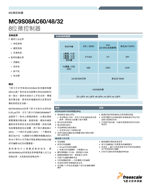
AC60結構框圖
實時中斷
6通道, 16位 2通道, 16位 2通道, 16位
定時器
16通道, 10位 ADC
ICE + BDM
ICG (20 MHz總線頻率)
如需其他信息,請參考飛思卡爾開發工具選擇指南(SG1011)。 * 顯示的價格為MSRP ** 須遵守許可協議
更多詳情: 如需瞭解關于AC系列的更多信息,請訪問:
/8-bit。
飛思卡爾™, Freescale™ and the Freescale logo are trademarks or registered trademarks of Freescale Semiconductor, Inc. in the U.S. and other countries. All other product or service names are the property of their respective owners. © Freescale Semiconductor, Inc. 2008. 文件編號: AC60FS REV 0
关于MC9S12系列用户手册

MC9S12系列器件说明MC9S12系列的名称定义(以MC9S12DJ64CFU为例):MC9S12:Controller Family 该控制器系列统称9:代表FLASHS12:内核型号DJ64:Device Title 器件名称64:64K的FLASHC:Temperature Options 温度选择FU:Package Option 封装结构选择温度选择表定义(Temperature Option):C = -40°C to 85°CV = -40°C to 105°CM = -40°C to 125°C封装结构选择定义(Package Options)FU = 80QFPPV = 112LQFP使用该系列芯片需遵循如下规则:寄存器:在不使用CAN0的情况下禁止读写CAN0寄存器(系统复位后地址范围:$0140 - $017F)。
在不使用BDLC的情况下禁止读写BDLC寄存器(系统复位后地址范围:$00E8 - $00EF)。
FAQ:BDLC?Byte Data Link Controller中断:在不使用CAN0的情况下,根据你的对未使用中断的编码方式,填满CAN0中断向量($FFB0 - $FFB7)。
在不使用BDLC的情况下,根据你的对未使用中断的编码方式,填满BDLC中断向量($FFC2, $FFC3)。
接口:在不使用CAN0的情况下,CAN0带TXCAN0, RXCAN0功能的引脚在PJ7, PJ6, PM5,PM4, PM3, PM2, PM1 和PM0接口上无效。
在不使用BDLC的情况下,BDLC功能引脚TXB, RXB在PM1和 PM0接口上无效。
FAQ:各引脚功能应该先有个介绍?在不使用CAN0的情况下,禁止写Module Routing Register的MODRR1 和MODRR0位。
MC9S12DJ64特征:·HCS12 核心:FAQ:HCS12?16-bit HCS12 CPUMEBI多路复用外部总线接口 (Multiplexed External Bus Interface)MMC模块映射控制 (Module Mapping Control)INT中断控制 (Interrupt control)BKP 断点(Breakpoints)BDM 后台调试模式(Background Debug Mode)·CRG (low current Colpitts or Pierce oscillator, PLL, reset, clocks, COP watchdog, real time interrupt, clock monitor)·8位和4位的带中断功能的接口:-数字滤波-可编程边缘触发(上升沿/下降沿)·存储器:-64K Flash EEPROM-1K byte EEPROM-4K byte RAM·2个八通道的数字/模拟转换器:-精度达到10bit-外部转换触发功能·1M bit/每秒,CAN2.0 A,B软件兼容模块:-5个接受和3个发送缓冲单元-Flexible identifier filter programmable as 2x32 bit, 4x16bit or 8x8bitFAQ:什么意思?-4个独立的中断通道,分别对应Rx, Tx, error 和 wake-up-低通滤波器唤醒功能-自测工作回送功能(Loop-back for self test operation)·增强了的捕捉时钟功能(Enhanced Capture Timer)-16位主计数器(7-bit prescaler)FAQ:prescaler?预定标器-8个可编程输入捕捉通道/输出比较通道-4个8位/2个16位脉冲累加器(pulse accumulator)·8个PWM通道:-周期和占空比系数可编程控制-8位八通道/16位4通道-独立的单个脉冲宽度和占空比控制-Center-aligned or left-aligned outputsFAQ:什么意思?-频率范围很广的可编程时钟选择逻辑单元-快速紧急关闭输入-可作为中断输入·串行接口:-2个异步SCI(Serial Communications Interfaces)-同步SPI(Serial Peripheral Interface)·Byte Data Link Controller(BDLC):-SAE J1850 Class B数据通信网络接口兼容,兼容应用于低速串行数据通信的ISO (SAEJ1850ClassBDataCommunicationsNetworkInterfaceCompatibleandISOCompatiblefor Low-Speed (<125 Kbps) Serial Data Communications in Automotive Applications)FAQ:什么意思?·Inter-IC Bus (IIC):I2总线标准-兼容C-多路控制工作(Multi-master operation)-软件可编程256个不同的串行始终频率·112引脚封装/80引脚封装-带驱动能力的5VI/O线路-5V A/D转换-50MHz工作频率,相当于25MHz总线速度-支持开发应用-单线程后台调试模块Obackground debug TM mode (BDM) -片上硬件断点调试(On-chip hardware breakpoints)模块框图:内存映射:图1-1与1-2芯片复位后的内存地址映射,1K的EEPROM被映射放大2倍分配到2K的地址空间里。
mc9s08fl8cbmDM60s芯片中文资料

mc9s08fl8cbmDM60s芯片中文资料MC9S08FL8CB芯片是由美国环球微电子公司生产的8位低功耗的HCS08微控制器,它的功能强大,配置高,节能性好,采用了目前芯片市场上最新的技术,功耗极低,寿命长,是一款非常受用户欢迎和青睐的芯片。
MC9S08FL8CB芯片采用先进的CMOS工艺技术,最高时钟频率可达20MHz,拥有多达64KBytes的Flash存储器,它处理速度快、运算能力强,可以满足复杂多变的应用环境需求,具有30个I/O口、可实现多种数据信号通讯、定时/多个模式及4个中断功能等等,同时具有PWM和UART模块,可实现各种多种控制和数字模拟互换功能,可以实现复杂的时序和控制操作。
MC9S08FL8CB芯片还具有采用智能温度监控电压管理技术的功率管理能力,可实现低功率运行,从而降低温度,降低功耗,适合有空间、能耗要求的精密设备的应用。
此外,它采用5V、3V电源设计,可实现范围内具有最佳兼容性和容错性以及高稳定性能。
MC9S08FL8CB芯片具有在各种工业控制、家用电器、消费产品和汽车电子领域有广泛用途,适用于有严格要求的低成本应用程序如家用小家电、安全显示仪器、汽车电子应用、医疗检测系统和各种紧凑型便携系统等。
基于其良好的高效性和功率低的特点,可以帮助设计人员实现数据的处理和转换,同时能够实现采用频谱效率最高的无线功耗要求。
总之,MC9S08FL8CB芯片具有低功耗、小尺寸、高性能、可靠、易于使用等特点,在低成本应用和工业系统设计中有着极大的用处。
环球微电子公司的MC9S08FL8CB芯片为现有系统的更新改造提供了更大的选择空间,为低成本的系统抗冲击提供了卓越的通用性和可靠性。
MC9S08JM60中文手册USB部分
第17章通用串行总线设备控制器 (S08USBV1)17.1 介绍这一章描述了通用串行总线设备控制器 (S08USBV1) 模块,它基于通用串行总线规格版本2.0。
该USB 总线设计目的是替代已经存在的用于PC 机外围设备的RS-232, PS/2, 和 IEEE 1284 总线。
这种S08USBV1 模块提供单片全速(12 Mbps)USB 设备应用的解决方案,而且集成了必需的带有串行接口引擎(SIE )的收发器,3.3-V 调节器, 端点RAM 和其他控制逻辑。
17.1.1 时钟要求S08USBV1需要两个时钟源,一个是24 MHz 总线时钟和一个48 MHz 基准时钟。
它的48 MHz 时钟是直接来自MCGOUT 。
为了获得48 MHz 的时钟速率, MCG 必需被恰当地配置成PLL 使能的外部(PEE) 模式,外接一晶振。
对于USB 操作,例如MCG 配置使用PEE 模式包括: • 2 MHz 晶振 – RDIV = 000 , VDIV = 0110 • 4 MHz 晶振 – RDIV = 001 , VDIV = 011017.1.2 在USB 挂起模式的电流消耗在USB 挂起模式,USB 设备的电流消耗被限制在500 μA 。
当USB 设备进入挂起模式,为了符合USB 挂起模式的电流消耗要求,固件通常进入停止3模式。
注意:允许LVD 将增加在停止模式3下的电流消耗。
因此,为了能满足USB 挂起模式的要求,在进入停止模式3前要禁止LVD 。
F RE E-TE C H飞锐泰克17.1.3 内部3.3V 稳压器如果使用一个外部3.3-V 调节器作为输入给V USB33 (仅仅当USBVREN = 0), 供应电压,V DD , 必须不能低于输入给V USB33引脚的电压。
如果使用内部3.3-V 调节器 (USBVREN = 1), 确保不要把外部供应电压连接到V USB33 引脚。
Freescale Semiconductor MC9S08QG8 4 8-bit 微控制器简介说明
OverviewThe MC9S08QG8/4 extends the advantages of FreescaleSemiconductor's HCS08 core to low pin count, small-package 8-bitmicrocontrollers. QG devices are low voltage with on-chip in-circuit Flash memory programmable down to 1.8V,and afford the standard features of all HCS08 MCUs includingwait mode and multiple stop modes.The functionality is completed with strong analog capabilities, a complete set of serial modules, a temperature sensor and robust memory options.Target Applications> Wireless sensor applications including SMAC > Watchdog coprocessors > Small appliances> Handheld devices > Secure boot coprocessors > Security systems 8-bit HCS08 Central Processor Unit (CPU)> Up to 10 MHz (bus frequency) HCS08 CPU (central processor unit) at >2.1V operation for 100 ns minimum instruction time and 8 MHz bus frequency at <2.1V operation> HC08 instruction set with added BGND instruction> Support for up to 32 interrupt/reset sources> Offering high performance, even at low voltage levels for battery-operated applications> Backward object-code compatibility with 68HC08and 68HC05 so existing code libraries can still be used > Allows for efficient, compact module coding in assembly or C compiler> Allows for software flexibility and optimization for real-time applicationsIntegrated Third-Generation Flash Memory and RAM> Provides users a single solution for multiple platforms or a single platform that is field reprogrammable in virtually any environment> Does not require additional pin or power supply for Flash programming, simplifying the interface for in-line programming and allowing for more GPIO pins> Helps reduce production programming costs through ultra-fast programming, as well as lowering system power consumption due to shorter writes> Allows EEPROM emulation, reducing system costs and board real estate> Internal clock source module (ICS) containing a frequency-locked loop (FLL) controlled by internal or external reference > Precision trimming of internal reference allows typical 0.1 percent resolution and +0.5 percent to -1 percent deviation over operating temperature and voltage > Internal reference can be trimmed from 31.25 kHz to 39.065 kHz, allowing for 8 MHz to 10 MHz FLL output> Low-power oscillator module (XOSC) with software selectable crystal or ceramic resonator range, 31.25 kHz to 38.4 kHz or 1MHz to 16 MHz, and supports external clock source input up to 20 MHz Flexible Clock Options> Can eliminate the cost of all external clock components, reduce board space and increase system reliability > Provides one of the most accurate internal clock sources on the market for the money> Can use trimming to adjust bus clocks for optimal serial communication baud rates and/or timer intervals > 32 kHz oscillator provides low power option for systems requiring time-keeping functionality (i.e., time and date) while in low power modes12 Bidirectional Input/Output (I/O) Lines; One Input Only and One Output Only Line> High-current I/O allows direct drive of LED and other circuits to virtually eliminate external drivers and reduce system costs > Reduces customer system cost by eliminating need for external resistors > Can configure ports for slower slew rate and weaker drive to minimize noise emissions from the MCU> Keyboard scan with programmable pull-ups/pull-downs virtually eliminate external glue logic wheninterfacing to simple keypads> Outputs 10 mA each; 60 mA max for package> Software selectable pull-ups on ports when used as input; internal pull-up on RESET and IRQ pin > Software selectable slew rate control and drive strength on ports when used as output> 8-pin keyboard interrupt module with software selectable polarity on edge or edge/level modes > Embedded Flash that is in-application reprogrammable over the full operating voltage and temperature range with a single power supply > Extremely fast, byte-writable programming; as fast as 20 us/byte > Up to 100,000 write/erase cycles at typical voltage and temperature (10k minimum write/erase); 100 years typical data retention (15 years minimum)Learn More: For more information about Freescale products, please visit .Freescale™ and the Freescale logo are trademarks of Freescale Semiconductor, Inc. All other product or service names are the property of their respective owners.These products incorporate SuperFlash technology licensed from SST.© Freescale Semiconductor, Inc. 2005MC9S08Q684FS REV 0Cost-Effective Development Tools For more information on development tools,please refer to the Freescale Development Tool Selector Guide (SG1011).DEMO9S08QG8 $50*Cost-effective demonstration board with potentiometer, LEDs, serial port and built-in USB-BDM cable for debugging and programming.M68CYCLONEPRO $99*HC08/HCS08/HC12/HCS12 stand-alone Flash programmer or in-circuit emulator,debugger, Flash programmer; USB, serial or Ethernet interface BMULTILINKBDM $99*Universal HC08 in-circuit debugger and Flash programmer; USB PC interface.CWX-H08-SE Free**CodeWarrior™ Special Edition for HC(S)08MCUs; includes integrated development environment (IDE), linker, debugger,unlimited assembler, Processor Expert™auto-code generator, full-chip simulation and 16 KB C compiler.Data SheetsMC9S08QG8Data Sheet for QG8/QG4Integrated Analog Peripherals> Easy interface to analog inputs, such as sensors > Used to set conversion complete and generate interrupt only when result matches condition> Can be used to run ADC when MCU clocks are off, such as in STOP3 low-power mode> Calculates temperature without any external components and saves an ADC input channel for other use > Constant voltage source for calibrating ADC results requires no external components> Takes periodic measurements without CPU involvement; can be used in STOP3 with compare function to take measurement and wake MCU from STOP3 only when compare level is reached> Flexible configuration to meet high performance and low power requirements> Requires only single pin for input signal> Allows other components in system to see results of comparator with minimal delay> Can be used for single slope ADC and RC time constant measurements> 8-channel, 10-bit analog-to-digital converter (ADC)• Automatic compare function, software programmable for greater than/equal to or less than conditions• Asynchronous clock source • Temperature sensor• Internal bandgap reference channel • Hardware triggerable using the RTI counter• Low-power and high-speed options> Analog comparator module (ACMP)• Option to compare to internal reference• Option to route comparator output directly to pin • Output can be optionally routed to TPM module as input capture triggerTwo Timer Modules> Programmable 16-bit timer/PWM module (TPM)> 8-bit modulo timer module (MTIM) with 8-bit prescalerSystem Protection> Resets device in instance of runaway or corrupted code, and independent clock source provides additional protection in case of loss of clock > Allows system to write/save important variables beforevoltage drops to low> Can hold device in reset until reliable voltage levels are reapplied to the part> Resets device in instance of runaway or corrupted code > Secures code sections so that it cannot be accidentally corrupted by runaway code > Option to protect various block sizes> Option to put bootloader code in protected space and clear Flash for reprogramming> Prevents unauthorized access to memory to protect a customer's valuable software IP> Significantly reduces risk of code runaway due to brownout situations> Watchdog computer operating properly (COP) reset with option to run from dedicated 1 kHz internal clock source or bus clock > Low-voltage detection with reset or interrupt> Illegal opcode detection with reset > Flexible block protection> Security feature for Flash and RAM > Always-on POR circuitry> SCI—serial communications interface module withoption for 13-bit break capabilities and double-buffered transmit and receive> SPI—serial peripheral interface module > I 2C—inter-integrated circuit bus moduleMultiple Serial Communication Options> All serial peripherals available for use in parallel on 16-pin devices> On-chip in-circuit emulation (ICE)Background Debugging System and On-Chip In-Circuit Emulation (ICE) with Real-Time Bus Capture> Provides single wire debugging and emulation interface; eliminates need for expensive emulation tools > Provides circuit emulation without the need for additional, expensive development hardware> One of the most flexible timer modules for the money; each channel can be independently programmable for input capture, output compare or buffered edge-aligned pulse width modulation (PWM) or buffered center-aligned PWM> Timer overflow interrupt can be enabled to generate periodic interrupts for time-based software loops*Prices indicated are MSRP.**Subject to license agreement and registration.Package OptionsPart Number Package Temp. Range MC9S08QG4CPAE 8-pin DIP -40°C to +85°C MC9S08QG4CDNE 8-pin SOIC-NB -40°C to +85°CMC9S08QG4CFQE 8-pin DFN -40°C to +85°C MC9S08QG4CDTE 16-pin TSSOP -40°C to +85°C MC9S08QG4CFFE 16-pin QFN -40°C to +85°C MC9S08QG8CDNE 8-pin SOIC-NB -40°C to +85°CMC9S08QG8CFQE 8-pin DFN -40°C to +85°C MC9S08QG8CPBE 16-pin DIP -40°C to +85°C MC9S08QG8CFFE 16-pin QFN -40°C to +85°C MC9S08QG8CDTE16-pin TSSOP-40°C to +85°CMC9S08QG Family available at -40°C to +125°C in 2H, 2006。
基于MC9S08SH4和AD7705的智能传感器系统设计

基于 MC S 8 H 9 0 S 4和 A 7 5的智 能传 感 器 系 统设 计 D70
王 艳 春 ,罗 少 轩
: l :
( 蚌埠 学 院 机 械 与 电子工 程 系 , 安徽 蚌 埠 2 3 3 ) 3 0 0
W ANG Ya Ch n un,LUO S a h o Xua n
( e a m n f Me h nc la d Ee t n n ier g e g u C l g , e g u 2 3 3 , hn ) D p r e to c a i n l r i E g e n ,B n b o e e B n b 3 0 0 C ia t a co c n i l
sf a rm r ie .F nt n u h a otae zr dute t l an aa poes g ot r f e ae gvn u ci s sc s sf r eo ajs n,f t g dt rcsi ,mut nds m aue e ta d R 一 w e a o w m oi n l - oe esrm n n S i
抗 干扰 能 力强 等优 点 。
关 键 词 :MC S 8 H 9 O S 4;AD 7 5;智 能 传 感 器 ;R 一 8 70 S 45
中 图 分 类 号 :T 2 2 P 1 文 献 标 识 码 :B
De in o n e lg n e s r s se b s d o sg f i t l e t s n o y t m a e n MC9 0 S n i S 8 H4 a d AD7 0 7 5
MC9S08QG8单片机的EEPROM虚拟技术
MC9S08QG8单片机的EEPROM虚拟技术引言MC9S08QG8(以下简称QG8)是Freeseale 公司于2006 年推出的一款HCS08 系列MCU。
HCS08 系列MCU 是HC08 系列的升级,具有更高的总线频率和更低的工作电压。
QG8 总线频率可以达到10 MHz,工作电压可以低至1.8 V,尤其是QG 系列MCU 采用了新型的Flash 存储器(HCS08 系列MCU 的典型型号为MC9S08GB/GT 系列MCU,Flash 编程擦除可使用2.7 V 电压,QG 系列MCU 工作在1.8 V 时即可以对Flash 进行操作)。
同时低功耗也是QG 系列MCU 的一大特点。
通过降低主频,在总线频率为1 MHz、供电电压2 V、温度125℃的情况下正常工作,典型的芯片电流仅有370μA。
而如果进入待机模式,典型的芯片电流则低于1 μA,这些特点使得QG8 非常适合使用在电池供电的设备中。
EEPROM 是Flash 存储技术成熟之前常用的存储器,它与Flash 均可作为程序存储器和数据存储器。
但由于EEPROM 本身容量和成本的限制,目前大多数MCU 都采用Flash 作为存储器。
用户可以在Flash 中存储设置参数、校准参数、保密数据等信息。
由于Flash 存储区的最小擦除单位是页(QG8 一页为512 字节),若存储数据长度小于一页,则每次写入或修改数据都必须进行一次页擦除操作,该页中没有用到的空间就浪费了。
相对而言,EEPROM 就不存在这个问题,它可以基于字节进行写入和擦除。
部分HC08 系列MCU(如MC68HC908JL8)为了解决这个问题,在其监控ROM 中提供了虚拟EEP 一ROM 的例程供用户使用。
但是QG8 不具有监控ROM,也就无法提供类似的功能,本文在QG8 擦除/写入Flash 的基础上,给出虚拟EEPROM 的实现机制和用户接口,实现按字节“写”Flash存储区的功能,提高Flash 存储器的使用效率及寿命。
- 1、下载文档前请自行甄别文档内容的完整性,平台不提供额外的编辑、内容补充、找答案等附加服务。
- 2、"仅部分预览"的文档,不可在线预览部分如存在完整性等问题,可反馈申请退款(可完整预览的文档不适用该条件!)。
- 3、如文档侵犯您的权益,请联系客服反馈,我们会尽快为您处理(人工客服工作时间:9:00-18:30)。
Reference Design OverviewMC9S08GW64Single-phase single-chip energy meterOverviewThe MC9S08GW is a low-power 8-bitmicrocontroller family, based on the provenS08 core, and used in gas or water flowmeters, as well as single-phase electricmeters. Two independent 16-bit SAR ADCswith a programmable delay block and a pulsecounter with automatic sensor decoding forgas and water flow meters make this familyideal for electric metering applications. Inaddition, the flexible LCD controller enablesit to be highly integrated. The MC9S08GWfamily comes with a full suite of hardware andsoftware tools to make development quick andeasy, including a cost-effective Tower modulefor rapid development.Feature list of MC9S08GW64• 8-bit HCS08 central processor unit (CPU)New, low power version of S08 core withsame performance as traditional S08Up to 20 MHz CPU at 3.6V to 2.1V and upto 10 MHz CPU at 2.1V to 1.8V, across atemperature range of -40°C to +85°CHC08 instruction set with added BGNDinstructionSupport for up to 48 interrupt/reset sources• On-chip memoryFlash read/program/erase over fulloperating voltage and temperatureRandom-access memory (RAM)Security circuitry to prevent unauthorizedaccess to RAM and flash contents• Clock source optionsOscillator (XOSC1): Loop-control Pierceoscillator, crystal or ceramic resonator of32.768 kHz, dedicated clock source foriRTC and optional for ICSOscillator (XOSC2): Loop-control Pierceoscillator, crystal or ceramic resonatorrange of 31.25 kHz to 38.4 kHz or 1 MHzto 16 MHz, optional clock source for ICS • System protectionWatchdog computer operating properly(COP) reset with option to run fromdedicated 1 kHz internal clock source orbus clockLow-voltage warning with interruptLow-voltage detection with reset orinterruptIllegal opcode and illegal addressdetection with resetFlash block protection• PeripheralsLCD: Up to 4 x 40 or 8 x 36 LCD driverwith internal charge pump and optionto provide an internally regulated LCDreference that can be trimmed forcontrast controlTwo analog-to-digital converters(ADCs): 16-bit resolution, one dedicateddifferential per ADC, up to 16-ch, upto 2.5 μs conversion time for 12-bitmode, automatic compare function,hardware averaging, calibration registers,temperature sensor, internal band gapreference channel, operation in stop3,fully functional from 3.6V to 1.8VThree rail to rail programmable referenceanalog comparators (PRACMP): Up toeight inputs, on-chip programmablereference generator output, selectableinterrupt on rising, falling, or either edgeof comparator output, operation in stop3 9S08GW 64/32 Block DiagramS08 Core LCD(1–8) x (43–36)Freescale and the Freescale logo are trademarks or registered trademarks of Freescale Semiconductor, Inc.,Reg. U.S. Pat. & Tm. Off. SMARTMOS is a trademark of Freescale Semiconductor, Inc. All other product or service names are the property of their respective owners. © 2010, Freescale Semiconductor, Inc.Document Number: SNGLPHSMTRRFFS / REV 0SCI: Four full duplex non-return to zero (NRZ), LIN master extended break generation, LIN slave extended break detection, wakeup on active edge, SCI0 designed for AMR operation, TxD of SCI1 and SCI2 can be modulated with timers and RxD can recieved through PRACMP SPI: Three full-duplex or single-wire bi-directional, double-buffered transmit and receive, master or slave mode, MSB-first or LSB-first shifting, SPI0 designed for AMR operationI 2C: Up to 100 kbps with maximum bus loading, multi-master operation, programmable slave address, interrupt driven byte-by-byte data transfer, supporting broadcast mode and 10-bit addressing, supporting SM BUS functionality, can wake up from STOP3FTM: 2-channel FTMs, selectable input capture, output compare, or buffered edge- or center-aligned PWM on each channelIndependent real-time clock (IRTC): Independent power domain, 32 bytes RAM, 32.768 kHz input clock optional output to ICS, hardware calendar, hardware compensation due to crystal or temperature characteristics, tamper detection and indicator 16/32-bit programmable cyclic redundancy check (PCRC): For high-speed CRC calculationMTIM: Two 8-bit and one 16-bit timers, configurable clock inputs and interrupt generation on overflowProgrammable delay block: Optimized for scheduling ADC conversionsPosition counter: Working in stop3 mode without waking CPU, can be used to generate timer waveforms • Input/output57 GPIOs including one output-only pin Eight KBI interrupts with selectable polarityHysteresis and configurable pull up device on all input pins, configurable slew rate and drive strength on all output pins • Package options80-pin LQFP , 64-pin LQFPOverviewThis reference design is suitable for energy or electricity meters which measure and display active energy (kWh) and apparent energy (kVAh). It also measures and displays voltage, current, frequency, power factor, active power (kW), reactive power (kVAr), apparent power (kVA), maximum demand in kW as well as time and date. All of the electrical parameters of the meter can be read using the optical port, which is based on the IEC62056. The meter can be calibrated and configured in different modes using the optical interface.Design Features• Based on MC9S08GW64• Supports IEC 62053-21, 62053-22 and IEC 620533-23• Shunt sensor for single phase, CT for detecting neutral missing tamper• Box-open tamper feature built in • Based on capacitive supply, meets 4 VA requirement• Measures and displays the following:RMS voltage (accuracy ±1% of full scale)RMS currents (accuracy ±1% of full scale)Net active power (accuracy ±1% of full scale)Net apparent power (accuracy ±1% of full scale)Power factor (accuracy ± 0.1 PF or better)Line frequency (accuracy ± 0.5 Hz or better)Tamper countActive energy: Class 1 or better Time and Date Maximum demand• Operating frequency range of 50 Hz ±3 Hz (230V , 5–30A model)• Measurement and storage of kWhMC9S08GW64 Single-Phase Electricity Meter Reference Design Block DiagramFreescale TechnologyOptional。
