HT7136A中文资料
HT7144A中文资料

HT71XXHigh Voltage RegulatorSelection TablePart No.Output VoltageToleranceHT7130 3.0V ±5%HT7133 3.3V ±5%HT7136 3.6V ±5%HT7144 4.4V ±5%HT71505.0V±5%1August 8,2000Features·Low power consumption ·Low voltage drop·Low temperature coefficient·High input voltage (up to 24V)·TO-92and SOT-89packagesApplications·Battery-powered equipment ·Communication equipment·Audio/Video equipmentGeneral DescriptionThe HT71XX series is a set of three-terminal low power high voltage regulators implemented in CMOS technology.They allow input voltages as high as 24V.They are available with several fixed output voltages ranging from 3.0V to 5.0V.CMOS technology ensures low voltage drop and low quiescent current.Although designed primarily as fixed voltage regulators,these devices can be used with ex-ternal components to obtainvariable voltages and currents.Block DiagramPin AssignmentPad Assignment Pad CoordinatesUnit:m m Pad No.X Y 1-480.00-451.50287.50-444.503482.00-444.50Chip size:1374´1294(m m)2*The IC substrate should be connected to VDD in the PCB layout artwork.2August 8,2000Absolute Maximum RatingsSupply Voltage..............................-0.3V to28V Storage Temperature................-50°C to125°C Power Consumption.............................200mW Operating Temperature.................0°C to70°CNote:These are stress ratings only.Stresses exceeding the range specified under Absolute Maxi-mum Ratings may cause substantial damage to the device.Functional operation of this de-vice at other conditions beyond those listed in the specification is not implied and prolonged exposure to extreme conditions may affect device reliability.Electrical CharacteristicsHT7130,+3.0V output typeHT7133,+3.3V output type Ta=25°C3August8,2000HT7144,+4.4V output type Ta=25°C4August8,2000Application CircuitsBasic circuits5August8,2000High output current positive voltage regulatorShort-Circuit protection by Tr1Circuit for increasing output voltageV V (1+R2R1)I R2OUT XX SS =+HT71XX6August 8,2000Circuit for increasing output voltageV OUT=V XX+V D1 Constant current regulatorI VR IOUTXXA SS=+Dual supply7August8,20008August 8,2000Copyright Ó2000by HOLTEK SEMICONDUCTOR INC.The information appearing in this Data Sheet is believed to be accurate at the time of publication.However,Holtek assumes no responsibility arising from the use of the specifications described.The applications mentioned herein are used solely for the purpose of illustration and Holtek makes no warranty or representation that such applications will be suitable without further modification,nor recommends the use of its products for application that may pres-ent a risk to human life due to malfunction or otherwise.Holtek reserves the right to alter its products without prior notification.For the most up-to-date information,please visit our web site at .Holtek Semiconductor Inc.(Headquarters)No.3Creation Rd.II,Science-based Industrial Park,Hsinchu,Taiwan,R.O.C.Tel:886-3-563-1999Fax:886-3-563-1189Holtek Semiconductor Inc.(Taipei Office)5F,No.576,Sec.7Chung Hsiao E.Rd.,Taipei,Taiwan,R.O.C.Tel:886-2-2782-9635Fax:886-2-2782-9636Fax:886-2-2782-7128(International sales hotline)Holtek Semiconductor (Hong Kong)Ltd.RM.711,Tower 2,Cheung Sha Wan Plaza,833Cheung Sha Wan Rd.,Kowloon,Hong Kong Tel:852-2-745-8288Fax:852-2-742-8657。
S7136中文资料

Equivalent Circuit
1. Vcc
1.27 Typ. 2.54±0.1.
3. OUT
1
0.7 Typ.
2
3
0.42 Typ.
3.0±0.1 3.8 Min.
2. GND
KSI-9036-000
1
元器件交易网
S7136AM
Absolute maximum ratings
Unit
V ㎽ ℃ ℃
Electrical Characteristics
Characteristic
Detecting voltage Low Level Output voltage Output Leakage Current Hysteresis Voltage Detecting Voltage Temperature Coefficient Circuit current at on Time Circuit current at off Time Threshold Operating Voltage 'L' Transmission Delay Time 'H' Transmission Delay Time Output Current at on Time I Output Current at on Time II
2
元器件交易网
S7136AM
Electrical Characteristic Curves
Fig. 1 VOUT –VCC Fig. 2 ICC -VCC
Fig. 3 ICCH-Temp
Fig. 4 IOL -RL
KSI-9036-000
3
Characteristic
HT71系列微功耗稳压器中文资料
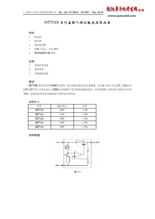
应用
y 电池供电设备 y 通讯设备 y 音频视频设备
概述
HT71XX 系列是采用 COMS 技术的三端口的低功耗高电压调整器 允许输入电压可达 24V 能输出从 3.0V-5.0V 的几个固定电压 COMS 技术确保了低压降和低静态电流 尽管检测器主要是设计成固定电压的 调整 但通过外围元件也能获得可变的电压和电流
引脚分布
图 1-2
广州周立功单片机发展有限公司 Tel 020 38730916 38730917 Fax 38730925
焊点分布
焊点坐标
表 1-2
芯片尺寸 1317 1294 um 22 工艺上 IC 衬底与 PCB 上的 VDD 相连
图 1-3
极限参数
注 这是极限参数 超出这些范围可导致设备内部损坏 其功能地实现 上述并未提到 下面将会有
详细的说明 在极限条件长时间运行会影响设备的可靠性
电气特性
HT7130,+3.0V 输出 表 1-3
பைடு நூலகம்
符号
参数 VIN
VOUT IOUT
VOUT
输出电压 5V 输出电流 5V 负载调节 5V
VDIF ISS
VOUT VIN× VOUT
最小
4.18 20 ― ― ―
―
―
―
典型值 4.4 30 60 100
0.2 ― ±0.7
最大 4.62
100 ― 7.5 ― 24 ―
单位 V mA mV mV uA %V
mV/
广州周立功单片机发展有限公司 Tel 020 38730916 38730917 Fax 38730925
增加输出电压电路
图 1-6
增加输出电压电路
HT7133A中文资料
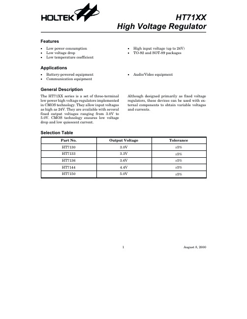
HT71XXHigh Voltage RegulatorSelection TablePart No.Output VoltageToleranceHT7130 3.0V ±5%HT7133 3.3V ±5%HT7136 3.6V ±5%HT7144 4.4V ±5%HT71505.0V±5%1August 8,2000Features·Low power consumption ·Low voltage drop·Low temperature coefficient·High input voltage (up to 24V)·TO-92and SOT-89packagesApplications·Battery-powered equipment ·Communication equipment·Audio/Video equipmentGeneral DescriptionThe HT71XX series is a set of three-terminal low power high voltage regulators implemented in CMOS technology.They allow input voltages as high as 24V.They are available with several fixed output voltages ranging from 3.0V to 5.0V.CMOS technology ensures low voltage drop and low quiescent current.Although designed primarily as fixed voltage regulators,these devices can be used with ex-ternal components to obtainvariable voltages and currents.Block DiagramPin AssignmentPad Assignment Pad CoordinatesUnit:m m Pad No.X Y 1-480.00-451.50287.50-444.503482.00-444.50Chip size:1374´1294(m m)2*The IC substrate should be connected to VDD in the PCB layout artwork.2August 8,2000Absolute Maximum RatingsSupply Voltage..............................-0.3V to28V Storage Temperature................-50°C to125°C Power Consumption.............................200mW Operating Temperature.................0°C to70°CNote:These are stress ratings only.Stresses exceeding the range specified under Absolute Maxi-mum Ratings may cause substantial damage to the device.Functional operation of this de-vice at other conditions beyond those listed in the specification is not implied and prolonged exposure to extreme conditions may affect device reliability.Electrical CharacteristicsHT7130,+3.0V output typeHT7133,+3.3V output type Ta=25°C3August8,2000HT7144,+4.4V output type Ta=25°C4August8,2000Application CircuitsBasic circuits5August8,2000High output current positive voltage regulatorShort-Circuit protection by Tr1Circuit for increasing output voltageV V (1+R2R1)I R2OUT XX SS =+HT71XX6August 8,2000Circuit for increasing output voltageV OUT=V XX+V D1 Constant current regulatorI VR IOUTXXA SS=+Dual supply7August8,20008August 8,2000Copyright Ó2000by HOLTEK SEMICONDUCTOR INC.The information appearing in this Data Sheet is believed to be accurate at the time of publication.However,Holtek assumes no responsibility arising from the use of the specifications described.The applications mentioned herein are used solely for the purpose of illustration and Holtek makes no warranty or representation that such applications will be suitable without further modification,nor recommends the use of its products for application that may pres-ent a risk to human life due to malfunction or otherwise.Holtek reserves the right to alter its products without prior notification.For the most up-to-date information,please visit our web site at .Holtek Semiconductor Inc.(Headquarters)No.3Creation Rd.II,Science-based Industrial Park,Hsinchu,Taiwan,R.O.C.Tel:886-3-563-1999Fax:886-3-563-1189Holtek Semiconductor Inc.(Taipei Office)5F,No.576,Sec.7Chung Hsiao E.Rd.,Taipei,Taiwan,R.O.C.Tel:886-2-2782-9635Fax:886-2-2782-9636Fax:886-2-2782-7128(International sales hotline)Holtek Semiconductor (Hong Kong)Ltd.RM.711,Tower 2,Cheung Sha Wan Plaza,833Cheung Sha Wan Rd.,Kowloon,Hong Kong Tel:852-2-745-8288Fax:852-2-742-8657。
QX7136中文版规格书
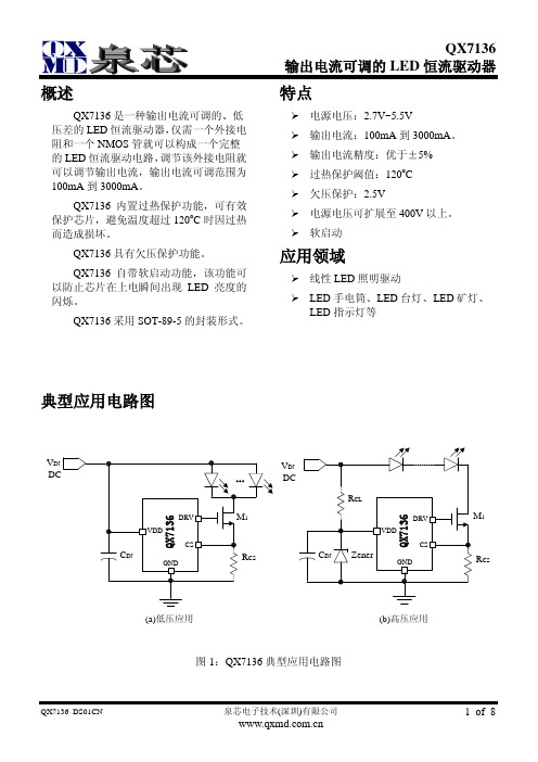
典型应用电路图DCR CS1V IN (a)低压应用V IN (b)高压应用图1:QX7136典型应用电路图概述QX7136是一种输出电流可调的、低压差的LED 恒流驱动器,仅需一个外接电阻和一个NMOS 管就可以构成一个完整的LED 恒流驱动电路,调节该外接电阻就可以调节输出电流,输出电流可调范围为100mA 到3000mA 。
QX7136内置过热保护功能,可有效保护芯片,避免温度超过120oC 时因过热而造成损坏。
QX7136具有欠压保护功能。
QX7136自带软启动功能,该功能可以防止芯片在上电瞬间出现LED 亮度的闪烁。
QX7136采用SOT-89-5的封装形式。
特点电源电压:2.7V~5.5V输出电流:100mA 到3000mA 。
输出电流精度:优于±5% 过热保护阈值:120o C欠压保护:2.5V电源电压可扩展至400V 以上。
软启动 应用领域线性LED 照明驱动LED 手电筒、LED 台灯、LED 矿灯、LED 指示灯等订货信息产品型号QX7136丝印7136XXXX批号年份封装及管脚分配SOT-89-57136 XXXX13254CSGND VDDDRV NC管脚定义内部电路方框图VDDCSDRVGND图2:QX7136的内部电路方框图极限参数(注1)注1:超过上表中规定的极限参数会导致器件永久性损坏。
而工作在以上极限条件下可能会影响器件的可靠性。
电特性除非特别说明,V IN =5V,T A =25o C电特性(接上一页)除非特别说明,V IN =5V , T A =25o C典型曲线除非特别说明,V IN =5V ,T A =25o C ,NMOS 管型号为AP2306。
应用指南工作原理QX7136是一种低静态电流、低压差的LED线性降压恒流驱动器。
通过采样输出电流作为负反馈来形成整个工作环路的稳定工作。
QX7136采用5.0V工艺制作,正常工作电压为3.0V到5.5V,当电源电压高过5.5V时通过外部的钳位电路使芯片工作电压钳位在5.5V即可满足高压大电流恒流LED驱动。
HT7150A中文资料

HT71XXHigh Voltage RegulatorSelection TablePart No.Output VoltageToleranceHT7130 3.0V ±5%HT7133 3.3V ±5%HT7136 3.6V ±5%HT7144 4.4V ±5%HT71505.0V±5%1August 8,2000Features·Low power consumption ·Low voltage drop·Low temperature coefficient·High input voltage (up to 24V)·TO-92and SOT-89packagesApplications·Battery-powered equipment ·Communication equipment·Audio/Video equipmentGeneral DescriptionThe HT71XX series is a set of three-terminal low power high voltage regulators implemented in CMOS technology.They allow input voltages as high as 24V.They are available with several fixed output voltages ranging from 3.0V to 5.0V.CMOS technology ensures low voltage drop and low quiescent current.Although designed primarily as fixed voltage regulators,these devices can be used with ex-ternal components to obtainvariable voltages and currents.Block DiagramPin AssignmentPad Assignment Pad CoordinatesUnit:m m Pad No.X Y 1-480.00-451.50287.50-444.503482.00-444.50Chip size:1374´1294(m m)2*The IC substrate should be connected to VDD in the PCB layout artwork.2August 8,2000Absolute Maximum RatingsSupply Voltage..............................-0.3V to28V Storage Temperature................-50°C to125°C Power Consumption.............................200mW Operating Temperature.................0°C to70°CNote:These are stress ratings only.Stresses exceeding the range specified under Absolute Maxi-mum Ratings may cause substantial damage to the device.Functional operation of this de-vice at other conditions beyond those listed in the specification is not implied and prolonged exposure to extreme conditions may affect device reliability.Electrical CharacteristicsHT7130,+3.0V output typeHT7133,+3.3V output type Ta=25°C3August8,2000HT7144,+4.4V output type Ta=25°C4August8,2000Application CircuitsBasic circuits5August8,2000High output current positive voltage regulatorShort-Circuit protection by Tr1Circuit for increasing output voltageV V (1+R2R1)I R2OUT XX SS =+HT71XX6August 8,2000Circuit for increasing output voltageV OUT=V XX+V D1 Constant current regulatorI VR IOUTXXA SS=+Dual supply7August8,20008August 8,2000Copyright Ó2000by HOLTEK SEMICONDUCTOR INC.The information appearing in this Data Sheet is believed to be accurate at the time of publication.However,Holtek assumes no responsibility arising from the use of the specifications described.The applications mentioned herein are used solely for the purpose of illustration and Holtek makes no warranty or representation that such applications will be suitable without further modification,nor recommends the use of its products for application that may pres-ent a risk to human life due to malfunction or otherwise.Holtek reserves the right to alter its products without prior notification.For the most up-to-date information,please visit our web site at .Holtek Semiconductor Inc.(Headquarters)No.3Creation Rd.II,Science-based Industrial Park,Hsinchu,Taiwan,R.O.C.Tel:886-3-563-1999Fax:886-3-563-1189Holtek Semiconductor Inc.(Taipei Office)5F,No.576,Sec.7Chung Hsiao E.Rd.,Taipei,Taiwan,R.O.C.Tel:886-2-2782-9635Fax:886-2-2782-9636Fax:886-2-2782-7128(International sales hotline)Holtek Semiconductor (Hong Kong)Ltd.RM.711,Tower 2,Cheung Sha Wan Plaza,833Cheung Sha Wan Rd.,Kowloon,Hong Kong Tel:852-2-745-8288Fax:852-2-742-8657。
3.6V稳压IC方案HT7136规格书

Features·Complete Data Transmission on Power Line functions·High Maximum Input Voltage:30V·Integrated Low Dropout Voltage Regulator·Integrated Voltage Detector for Power Supply Monitoring·Open drain NMOS drivers for flexible interfacing·Power and Reset Protection Features·8-pin SOP package type·Minimal external component requirementsGeneral DescriptionIn systems where a master controller controls a number of individual interconnected subsystems suchas found in smoke detector systems,water metering systems,solar energy system etc.,the cost of thelengthy interconnecting cabling can be a major factor.By sending data along the power supply lines,the interconnecting cables can be reduced to a simple two line type,thus greatly reducing both cableand installation costs.With a the addition of a few external components,this power line data transceiver device contains allthe internal components required to provide users with a system for power line data transmission andreception.Data is modulated onto the power line by the simple reduction of the power line voltage fora specific period of time.Power supply voltage changes can be initiated by the master controller fordata reception or initiated by the HT71D0x devices for data transmission.An internal voltageregulator within the device ensures that a constant voltage power supply is provided to theinterconnected subsystem units while an internal voltage detector monitors the power line voltagelevel.Selection GuideRev.1.001June30,2010Block DiagramPin AssignmentRev.1.002June 30,2010HT71D02/HT71D04Power Line DataTransceiverVINCNCP/TDCXCDLYVOVSS/TSPin DescriptionCP and TD share the same pinAbsolute Maximum RatingsMaximum Input Supply V oltage..................................................................................................33V Operating Temperature................................................................................................-40°C to 85°C Storage Temperature .................................................................................................-55°C to 150°C Maximum Junction Temperature..............................................................................................150°CNote:These are stress ratings only.Stresses exceeding the range specified under ²Absolute Maximum Ratings ²may cause substantial damage to the device.Functional operation of this device at other conditions beyond those listed in the specification is not implied and prolonged exposure to extreme conditions may affect device reliability.D.C.CharacteristicsTa=25°CHT71D02/HT71D04Power Line Data TransceiverRev.1.003June 30,2010Note:1.D V OUT is calculated as the difference between the output voltage under testing and the output voltage which is measured at I OUT =10mA.2.V IO specification is design guaranteed.Rev.1.004June 30,2010HT71D02/HT71D04Power Line Data TransceiverFunctional DescriptionThese devices provide a way to transmit and receive data on the common power lines of an interconnected array of microcontroller based subsystems.By having one of these devices inside each subsystem,the shared power and data cabling can be reduced to a simple two line type,offering major installation cost reductions.Shared Power LineAll microcontroller based subsystems are connected together via the same two line power connection.The ground line is hardwired to each subsystem while the positive power line is connected to the VIN pin on each of the HT71D0x devices.An internal Low Dropout V oltage Regulator within the HT71D0x devices,converts this input power supply voltage to a fixed voltage level which is supplied to the subsystem microcontroller and other circuit components.In this way when the power line voltage is changed due to the transmission or reception of data the subsystem circuits still continue to receive a regulated power supply.HT71D02/HT71D04Power Line Data TransceiverRev.1.005June 30,2010System Block DiagramData TransmissionRefer to the application circuit when reading the following description.Data information can be transmitted onto the positive power line by reducing the voltage level for a short time duration.As the devices include a voltage regulator which is used as the power supply to the subsystem units,then the subsystem power supply voltage will not be affected as long as the regulator minimum dropout voltage is maintained.However a reduction in the power supply will be detected by the C1internal comparators.The output of this comparator is connected to an open drain NMOS transistor,Q1,whose open drain output on pin CX can be connected to a microcontroller input for use as a data signal.Data ReceptionRefer to the application circuit when reading the following description.The individual subsystems can transmit data to the master controller along the power supply line by using one of its I/O lines to reduce the positive power line supply line voltage level for a short time duration.An output line on the subsystem microcontroller should be connected to the TG pin.An internal comparator,C2,whose positive input is connected to an internal voltage reference,will detect if this pin is pulled low.The comparator output is connected to an internal open drain NMOS transistor,Q4,which will pull the CP/TD line low.By connecting a suitable value resistor between the CP/TD pin and the power supply line,the correct value of power supply voltage reduction can be implemented.Protection CircuitsThe devices include an internal V oltage Detector function which monitors the power supply input voltage.Should the input power supply voltage fall below a safe level specified by the voltage detector level,then the voltage detector output will change state and disable the internal regulator thus removing the power supply source to the subsystem circuits.An internal NMOS transistor whose drain is connected to the output power supply line,VO will also turn on keeping the VO level close to zero.This ensures that the subsystem microcontroller receives the proper power on reset conditions.When power is applied an external capacitor,connected to pin CDLY ,together with an internal resistor,RPU1,implement a power on delay time for the internal LDO.Rev.1.006June 30,2010HT71D02/HT71D04Power Line DataTransceiverPower Line Data ReceptionApplication ConsiderationsIt is envisaged that the devices will be used together with microcontroller based subsystems which willbe required to provide two I/O pins for data transmission and reception.The MCU pin connected to theTG pin must be setup as an output while the MCU pin connected to the CX pin must be setup as aninput.The power supply impedence will play an important role in applications using these devices and mustbe well defined for reliable data transmission and reception.The external components connected to the CP/TD pin must be chosen carefully to ensure that anadequate pulse duration on pin CX is generated.The usual decoupling precautions must be taken to ensure reliable operation.Application CircuitsThe following application circuit shows the device used in conjunction with a microcontroller.Rev.1.007June30,2010Package Information8-pin SOP(150mil)Outline DimensionsMS-012Rev.1.008June30,2010Reel DimensionsSOP8NRev.1.009June30,2010Carrier Tape DimensionsSOP8NRev.1.0010June30,2010HT71D02/HT71D04Power Line Data TransceiverRev.1.0011June30,2010。
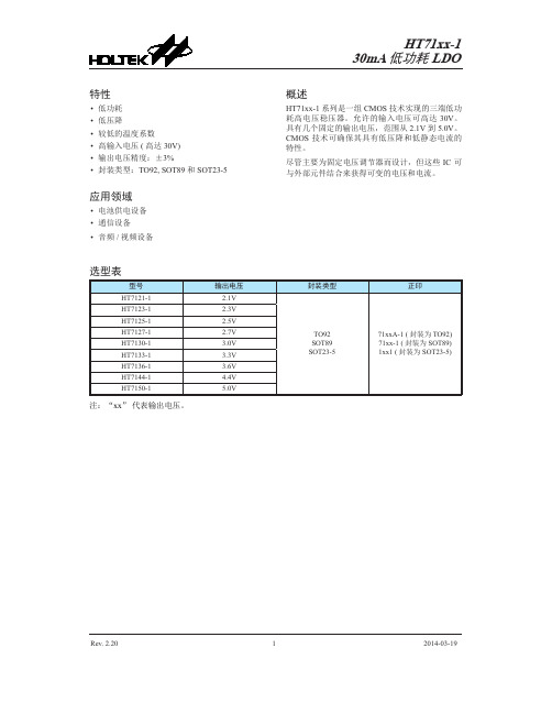
HT7133规格书
—
35
55
mV
ISS
D V OUT D V IN ´ V O U T
耗电流 输入电压调节率
5.3V 无负载
—
2.5
4.0
— 4.3V ≤ VIN ≤ 30V, IOUT=1mA
—
0.1
0.2
µA %/V
VIN
输入电压
—
—
—
—
30
V
D V OUT D T a´ V O U T
温度系数
5.3V IOUT=10mA, -40°C<Ta<85°C
5.6V 1mA ≤ IOUT ≤ 30mA — IOUT=1mA, ∆ VOUT=2% 5.6V 无负载
— 4.6V ≤ VIN ≤ 30V, IOUT=1mA
—
—
5.6V IOUT=10mA, -40°C<Ta<85°C
—
15
45
mV
—
35
55
mV
—
2.5
4.0
µA
—
0.1
0.2
%/V
—
—
30
V
Rev. 2.20
6
2014-03-19
HT71xx-1
HT7150-1, +5.0V 输出类型
Ta=25°C
符号
参数
测试条件
VIN
条件最小Biblioteka 典型 最大单位VOUT
输出电压
7V IOUT=10mA
4.850 5.00 5.150
V
IOUT
输出电流
7V
—
20
30
—
mA
∆ VOUT
HT7136-1中文资料

HT71XX-130mA Voltage RegulatorSelection TablePart No.Output VoltageTolerance PackageMarkingHT7130-1 3.0V ±3%TO-92SOT-89SOT-2571XXA-1(for TO-92)71XX-1(for SOT-89)1XX1(for SOT-25)HT7133-1 3.3V ±3%HT7136-1 3.6V ±3%HT7144-1 4.4V ±3%HT7150-15.0V±3%Note:²XX ²stands for output voltages.Block DiagramRev.1.101August 22,2002Features·Low power consumption ·Low voltage drop·Low temperature coefficient·High input voltage (up to 24V)·Output voltage accuracy:tolerance ±3%·TO-92,SOT-89and SOT-25packageApplications·Battery-powered equipment ·Communication equipment·Audio/Video equipmentGeneral DescriptionThe HT71XX-1series is a set of three-terminal low power high voltage regulators implemented in CMOS technology.They allow input voltages as high as 24V.They are available with several fixed output voltages ranging from 3.0V to 5.0V.CMOS technology ensures low voltage drop and low quiescent current.Although designed primarily as fixedvoltage regulators,these devices can be used with external components to obtain variable voltages and currents.VOUTVINGNDV refPin AssignmentPad Assignment Pad Coordinates Unit:m mPad No.X Y1-429.00-401.002123.50-401.003416.00-401.00Chip size:1111´1051(m m)2*The IC substrate should be connected to VDD in the PCB layout artwork.Absolute Maximum RatingsSupply Voltage.........................................-0.3V to26V Storage Temperature...........................-50°C to125°C Power Consumption(*1)..................................200mW Operating Temperature..............................0°C to70°C Power Consumption(*2)...................................150mWNote:These are stress ratings only.Stresses exceeding the range specified under²Absolute Maximum Ratings²may cause substantial damage to the device.Functional operation of this device at other conditions beyond those listed in the specification is not implied and prolonged exposure to extreme conditions may affect device reliabil-ity.*1:applied to SOT-89and TO-92*2:applied to SOT-25Rev.1.102August22,2002Electrical CharacteristicsHT7130-1,+3.0V output type Ta=25°CHT7133-1,+3.3V output type Ta=25°CHT7136-1,+3.6V output type Ta=25°CRev.1.103August22,2002HT7144-1,+4.4V output type Ta=25°CHT7150-1,+5.0V output type Ta=25°CApplication CircuitsBasic circuitsRev.1.104August22,2002High output current positive voltage regulatorShort-Circuit protection by Tr1Circuit for increasing output voltageV V(1+R2R1)I R2OUT XX SS=+Rev.1.105August22,2002Circuit for increasing output voltageV OUT=V XX+V D1 Constant current regulatorIOUTXXA SSV R I=+Dual supplyRev.1.106August22,2002Package Information3-pin TO-92outline dimensionsSymbolDimensions in milMin.Nom.Max.A170¾200B170¾200C500¾¾D11¾20E90¾110F45¾55G45¾65H130¾160I8¾18a4°¾6°Rev.1.107August22,2002SymbolDimensions in milMin.Nom.Max.A173¾181B64¾72C90¾102D35¾47E155¾167F14¾19G17¾22H¾59¾I55¾63J14¾17Rev.1.108August22,2002SymbolDimensions in mmMin.Nom.Max.A 1.00¾ 1.30A1¾¾0.10A20.70¾0.90b0.35¾0.50C0.10¾0.25D 2.70¾ 3.10E 1.40¾ 1.80e¾ 1.90¾H 2.60¾3L0.37¾¾q1°¾9°Rev.1.109August22,2002Product Tape and Reel SpecificationsTO-92reel dimensions(Unit:mm)Rev.1.1010August22,2002SOT-89Symbol Description Dimensions in mmA Reel Outer Diameter180±1.0B Reel Inner Diameter62±1.5C Spindle Hole Diameter12.75+0.15D Key Slit Width 1.9±0.15T1Space Between Flange12.4+0.2T2Reel Thickness17-0.4SOT-25Symbol Description Dimensions in mmA Reel Outer Diameter178±1.0B Reel Inner Diameter62±1.0C Spindle Hole Diameter13.0±0.2D Key Slit Width 2.5±0.25T1Space Between Flange 8.4+1.5-0.0T2Reel Thickness11.4+1.5Rev.1.1011August22,2002TO-92Symbol Description Dimensions in mm I1Taped Lead Length(2.5)P Component Pitch12.7±1.0P0Perforation Pitch12.7±0.3P2Component to Perforation(Length Direction) 6.35±0.4F1Lead Spread 2.5+0.4-0.1F2Lead Spread 2.5+0.4-0.1D h Component Alignment0±0.1W Carrier Tape Width 18.0+1.0-0.5W0Hold-down Tape Width 6.0±0.5W1Perforation Position9.0±0.5W2Hold-down Tape Position(0.5)H0Lead Clinch Height16.0±0.5H1Component Height Less than24.7D0Perforation Diameter 4.0±0.2t Taped Lead Thickness0.7±0.2H Component Base Height19.0±0.5Note:Thickness less than0.38±0.05mm~0.5mmP0Accumulated pitch tolerance:±1mm/20pitches.()Bracketed figures are for consultation onlyRev.1.1012August22,2002SOT-89&SOT-25carrier tape dimensionsSOT-89Symbol Description Dimensions in mmW Carrier Tape Width 12.0+0.3-0.1P Cavity Pitch8.0±0.1E Perforation Position 1.75±0.1F Cavity to Perforation(Width Direction) 5.5±0.05D Perforation Diameter 1.5+0.1D1Cavity Hole Diameter 1.5+0.1P0Perforation Pitch 4.0±0.1P1Cavity to Perforation(Length Direction) 2.0±0.10A0Cavity Length 4.8±0.1B0Cavity Width 4.5±0.1K0Cavity Depth 1.8±0.1t Carrier Tape Thickness0.30±0.013C Cover Tape Width9.3SOT-25Symbol Description Dimensions in mmW Carrier Tape Width 8.0+0.3-0.3P Cavity Pitch 4.0E Perforation Position 1.75F Cavity to Perforation(Width Direction) 3.5±0.05D Perforation Diameter 1.5+0.1D1Cavity Hole Diameter 1.5+0.1P0Perforation Pitch 4.0P1Cavity to Perforation(Length Direction) 2.0A0Cavity Length 3.15B0Cavity Width 3.2K0Cavity Depth 1.4t Carrier Tape Thickness0.20±0.03C Cover Tape WidthRev.1.1013August22,2002Holtek Semiconductor Inc.(Headquarters)No.3,Creation Rd.II,Science-based Industrial Park,Hsinchu,TaiwanTel:886-3-563-1999Fax:886-3-563-1189Holtek Semiconductor Inc.(Sales Office)11F,No.576,Sec.7Chung Hsiao E.Rd.,Taipei,TaiwanTel:886-2-2782-9635Fax:886-2-2782-9636Fax:886-2-2782-7128(International sales hotline)Holtek Semiconductor(Shanghai)Inc.7th Floor,Building2,No.889,Yi Shan Rd.,Shanghai,ChinaTel:021-6485-5560Fax:021-6485-0313Holtek Semiconductor(Hong Kong)Ltd.RM.711,Tower2,Cheung Sha Wan Plaza,833Cheung Sha Wan Rd.,Kowloon,Hong KongTel:852-2-745-8288Fax:852-2-742-8657Holmate Semiconductor,Inc.48531Warm Springs Boulevard,Suite413,Fremont,CA94539Tel:510-252-9880Fax:510-252-9885CopyrightÓ2002by HOLTEK SEMICONDUCTOR INC.The information appearing in this Data Sheet is believed to be accurate at the time of publication.However,Holtek as-sumes no responsibility arising from the use of the specifications described.The applications mentioned herein are used solely for the purpose of illustration and Holtek makes no warranty or representation that such applications will be suitable without further modification,nor recommends the use of its products for application that may present a risk to human life due to malfunction or otherwise.Holtek reserves the right to alter its products without prior notification.For the most up-to-date information,please visit our web site at .Rev.1.1014August22,2002。
H-1-3-6TV-B型铝箔智能测试仪使用说明书

跟着是RS-232 接口我们只利于了其中的3 根线RXD TXD GND 管脚排列如上图所示 管脚号 信号 2 ---RXD 3--- TXD 5--- GND
四、操作说明
硬件部分
1.1 仪器接收检查:
-10℃ ~+ 40℃
20%~85%
A 型系列电流手动调节,电压、电流的采样和控制全部 自动(面板带电流控制电位器)适合 TV 测试
B 型系列电压、电流的采样和控制全部自动(取消面板 电流电位器),增加漏电流,电解液等测试功能
C 型系列在 B 型系列基础上增加了阶梯电压等元器件耐 压检测功能。可以借助仪器测试电容、三极管等元器件的极限 参数、鉴别元器件的好坏等。
7
输入电压
8
环境温度
9
相对湿度
10
控制方式
11
放电时间
12
放电电压
13
产品保修
14
通讯方式
15
数据库
16
数据查询
17
数据打印
18
扩展功能
19
定制产品
20
通用产品
30V-1000V(1‰)中高压(订货时需注 高压任意组合。 明)
0-10mA(1‰) 如 >10mA 可定制 5.7 寸液晶屏 AC220±10%,50Hz±10%
1.1 光盘放入 CDROM 中,打开光盘,再双击右边图标, 将在您的计算机上安装“铝箔测试仪”软件,请根据提示完成本 软件的安装。(为保障不同系统数据畅通,如果您的机器未安装 VB6.0,请安装光盘上的 微型版 VB6.0)
SH7133线性稳压器LDO完全兼容HT7133

4.850
5.0 5.150 V
输出电流
IOUT
VIN=VOUT+2.0V
100
150
— mA
负载调整率 低压差
△VOUT VDIF
VIN=VOUT+2.0V 1mA≤IOUT≤70mA
IOUT=1mA,△VOUT=2%
—
25
60 mV
—
25
55 mV
静态电流
ISS
无负载
—
1.5
3.0 μA
线性调整率
最大额定值
参数说明
符号
数值范围
单位
工作电压
VIN
-0.3~+28
V
贮存温度
TSTG
-50~+125
℃
工作温度
TA
-40~+85
℃
注意:如果器件运行条件超过上述各项最大额定值,可能对器件造成永久性损坏。上述参数仅是运
行条件的极大值,我们不建议器件在该规范范围外运行。如果器件长时间工作在绝对最大极限条件
IOUT=1mA,△VOUT=2%
—
25
60 mV
—
25
55 mV
静态电流
ISS
无负载
—
1.5
3.0 μA
线性调整率
△VOUT/ VOUT* △VIN
VOUT+1.0V≤VIN≤24V, IOUT=1mA
—
—
0.2 %/V
输入电压
VIN
—
—
—
24
V
温度系数
△VOUT/ △TA*VOUT
VIN= VOUT+2.0V,IOUT=10mA, -40℃≤TA≤85℃
TDA7056A中文资料

THERMAL RESISTANCE 55 K/W 10 K/W
Note to the thermal resistance
VP = 12 V; RL = 16 Ω; The maximum sine-wave dissipation is = 1.8 W. The Rth vj-a of the package is 55 K/W; Tamb (max) = 150 − 55 x 1.8 = 51 °C
EXTENDED TYPE NUMBER
TDA7056A
PINS 9
Note 1. SOT110-1; 1996 August 21.
PIN POSITION SIL
PACKAGE MATERIAL plastic
CODE SOT110
July 1994
2
元器件交易网
Philips Semiconductors
3 W BTL mono audio output amplifier with DC volume control
Product specificiation
TDA7056A
handbook, full pagewidth
n.c.
1
n.c.
9
positive input
3
5 DC volume control
7 power ground
8 negative output
9 not connected
handbook, halfpage
n.c. 1
VP 2 VI 3 GND1 4
VC 5 TDA7056A
OUT+ 6
GND2 7
OUT− 8
n.c. 9
TC7136CKW资料

Typical Segment Input V+ 0.5mA Segment Output LCD 2mA
DS21461B-page 4
Internal Digital Ground
Functional Block Diagram
TC7136/A
RINT VREFCREF- VBUFF V 28 Integrator – + –
D2
34 G1
TC7136CPL TC7136ACPL
C2 10 10's B2 11 A2 12
ANALOG 9 COMMON VIN+ 10 VIN- 11 CAZ VBUFF VINT VG2 C3 A3 12 13 14 15 16 17 18
TC7136RCPL TC7136ARCPL
33 E1 32 D2 31 C2 30 B2 29 A2 28 F2 10's
F2 13 E2 14
27 E2 26 D3 25 B3 24 F3 100's
D3 15 100's B3 16
F3 17 E3 18 19
23 E3 22 AB4 1000's
1000's
AB4
G3 19 BP 20 (Backplane)
POL 20 (MINUS SIGN)
21 POL (Minus Sign)
6.2V
ANALOG COMMON
32
DE (+)
+
V+
AZ & DE (±) 26 V40 OSC1 39 OSC2 ROSC 38 OSC3 COSC
VINInternal Digital Ground VTH = 1V 500Ω
7136数显温度计

在这里,我向大家介绍LCD数显温度计的制作。
它用二极管IS1588做温度传感器,测温范围在+150°C到-20°C之间,如采用集成电路温度传感器S800,测温范围在+100到-40°C之间。
这里我们介绍用二极管IS1588做温度传感电路接线图注:橄榄绿颜色的线表示连线在元件侧。
R4 (绿)为附加的元件。
红色的线为附加的小数点连线。
粉红色的线表示外接器件。
工作原理介绍下面的将用提问的方式来解释这款数显温度计的工作原理。
但愿这样可能让人更容易理解其原理。
为什么可以用二极管来测量温度?我们知道,硅二极管有个特性是:当环境温度改变时,其PN结的正向电压降Vf以-2mV/°C 改变(如右图示)。
通常,20°C时,其Vf约600mV。
当环境温度增加100°C时,既从20°C变化到120°C时,这时其正向电压降Vf约为400mV(600mV-(2mV/°C*100°C))。
这里介绍的温度计,就是检测二极管Vf电压的变化来实现温度检测。
由此可以看出,电路的测温范围取决于二极管许可的工作范围。
不同的二极管测温范围不同,但大多数的二极管可以测量的范围在-20°C到150°C左右。
还有,由于的二极管的一般都有玻璃或塑料材料封装,所以但环境温度变化时,二极管的Vf不会很快改变。
iICL7136是什么样的集成电路?ICL7136 是一种用于测量输入电压的CMOS型集成电路。
它内部包含驱动LCD(Liquid Crystal Display)液晶显示屏电路。
测量电压范围在±200 mV 到±2 V之间。
另外,另一种功能类似集成电路ICL7137可以直接驱动LED数码显示管。
LCD的控制信号是频率为60 Hz(48KHz/800)、电压为5.5Vp-p的方波信号。
测量的输入电压被转换成一定时间下的电能(即电容的放电时间)。
XH716A说明书(1600)
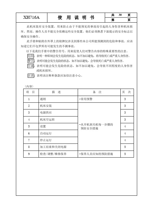
〈内容〉 项 1 2 3 4 5 6 7 8 9 目 通则 机床安装 电源供应 机床空运转 设置 自动运行 停止运行 加工结束和关闭电源 检查/调整/维修保养 -保养人员应知的预防措施 -从开机到关机每一步骤的 预防安全措施 描 述 -常用预警 备 注 页 3 3 3 3 4 4 4 5 5 次
XH716A
共 第
30
页 页
1. 产品型号、名称、外观图
XH716A 立式加工中心是一种中大型规格、高效通用自动化机床。该机床配有先进的 FANUC-OIMB 数控系统,具有 CNC 标准功能,主传动采用αp30 可换档的交流伺服主轴电 机,经 1:1 的主电机带轮和主轴带轮及 8YU 园弧齿形带传动,主轴低速扭矩可达 249Nm。该机床大件采用稠筋封闭式框架结构,刚性高、抗震性好。三向导轨采用淬硬精 磨与 Turcite-B 贴塑导轨副,导轨接触精度高,无低速爬行现象,并具有良好的耐磨性 和精度保持性。三向进给采用零间隙预负荷精密滚珠丝杆副和预拉伸安装方式,进给系 统采用全数字交流伺服电机,并装有同轴编码器,构成位置及速度信息反馈半闭环伺服 控制系统,保证了机床加工时的定位精度和工作精度。机床配装 24 把刀的圆盘式刀库, 机械手换刀以满足切削时快速换刀的需要。 该机床为机电一体化三轴立式加工中心(可加第四轴)。用途广泛,功能齐全,对 零件的适应性强, 可进行铣削、镗削、钻削、铰孔、攻丝等多种切削加工;由于主轴低 速扭矩大,特别适合于加工余量大且具有复杂外形或型腔的中大型工件和模具以及凸 轮、样板等各种机械零件的加工。 3. 机床的主要规格参数 3.1 工作台 工作台面………………………………………………………1600×630mm T 型槽数及宽度………………………………………………………5×18H8mm T 型槽间距…………………………………………………………………100mm 工作台允许最大承重………………………………………………………1500kg 3.2 主轴 主轴孔锥度………………………………………………BT50 (ISO50# 7:24) 主轴转速范围………………………………………………………50~5000rpm 3.3 机械极限行程 纵向(X 向)………………………………………………………………1300mm 横向(Y 向)………………………………………………………………650mm 垂向(Z 向)…………………………………………………………710mm 主轴端面至工作台面距离…………………………………………120~830mm 主轴中心至立柱导轨面距离……………………………………………680mm 3.4 进给速度 进给速度范围……………………………………………………1~5000mm/min
HT7144-1资料

HT71XX-130mA Voltage RegulatorSelection TablePart No.Output VoltageTolerance PackageMarkingHT7130-1 3.0V ±3%TO-92SOT-89SOT-2571XXA-1(for TO-92)71XX-1(for SOT-89)1XX1(for SOT-25)HT7133-1 3.3V ±3%HT7136-1 3.6V ±3%HT7144-1 4.4V ±3%HT7150-15.0V±3%Note:²XX ²stands for output voltages.Block DiagramRev.1.101August 22,2002Features·Low power consumption ·Low voltage drop·Low temperature coefficient·High input voltage (up to 24V)·Output voltage accuracy:tolerance ±3%·TO-92,SOT-89and SOT-25packageApplications·Battery-powered equipment ·Communication equipment·Audio/Video equipmentGeneral DescriptionThe HT71XX-1series is a set of three-terminal low power high voltage regulators implemented in CMOS technology.They allow input voltages as high as 24V.They are available with several fixed output voltages ranging from 3.0V to 5.0V.CMOS technology ensures low voltage drop and low quiescent current.Although designed primarily as fixedvoltage regulators,these devices can be used with external components to obtain variable voltages and currents.VOUTVINGNDV refPin AssignmentPad Assignment Pad Coordinates Unit:m mPad No.X Y1-429.00-401.002123.50-401.003416.00-401.00Chip size:1111´1051(m m)2*The IC substrate should be connected to VDD in the PCB layout artwork.Absolute Maximum RatingsSupply Voltage.........................................-0.3V to26V Storage Temperature...........................-50°C to125°C Power Consumption(*1)..................................200mW Operating Temperature..............................0°C to70°C Power Consumption(*2)...................................150mWNote:These are stress ratings only.Stresses exceeding the range specified under²Absolute Maximum Ratings²may cause substantial damage to the device.Functional operation of this device at other conditions beyond those listed in the specification is not implied and prolonged exposure to extreme conditions may affect device reliabil-ity.*1:applied to SOT-89and TO-92*2:applied to SOT-25Rev.1.102August22,2002Electrical CharacteristicsHT7130-1,+3.0V output type Ta=25°CHT7133-1,+3.3V output type Ta=25°CHT7136-1,+3.6V output type Ta=25°CRev.1.103August22,2002HT7144-1,+4.4V output type Ta=25°CHT7150-1,+5.0V output type Ta=25°CApplication CircuitsBasic circuitsRev.1.104August22,2002High output current positive voltage regulatorShort-Circuit protection by Tr1Circuit for increasing output voltageV V(1+R2R1)I R2OUT XX SS=+Rev.1.105August22,2002Circuit for increasing output voltageV OUT=V XX+V D1 Constant current regulatorIOUTXXA SSV R I=+Dual supplyRev.1.106August22,2002Package Information3-pin TO-92outline dimensionsSymbolDimensions in milMin.Nom.Max.A170¾200B170¾200C500¾¾D11¾20E90¾110F45¾55G45¾65H130¾160I8¾18a4°¾6°Rev.1.107August22,2002SymbolDimensions in milMin.Nom.Max.A173¾181B64¾72C90¾102D35¾47E155¾167F14¾19G17¾22H¾59¾I55¾63J14¾17Rev.1.108August22,2002SymbolDimensions in mmMin.Nom.Max.A 1.00¾ 1.30A1¾¾0.10A20.70¾0.90b0.35¾0.50C0.10¾0.25D 2.70¾ 3.10E 1.40¾ 1.80e¾ 1.90¾H 2.60¾3L0.37¾¾q1°¾9°Rev.1.109August22,2002Product Tape and Reel SpecificationsTO-92reel dimensions(Unit:mm)Rev.1.1010August22,2002SOT-89Symbol Description Dimensions in mmA Reel Outer Diameter180±1.0B Reel Inner Diameter62±1.5C Spindle Hole Diameter12.75+0.15D Key Slit Width 1.9±0.15T1Space Between Flange12.4+0.2T2Reel Thickness17-0.4SOT-25Symbol Description Dimensions in mmA Reel Outer Diameter178±1.0B Reel Inner Diameter62±1.0C Spindle Hole Diameter13.0±0.2D Key Slit Width 2.5±0.25T1Space Between Flange 8.4+1.5-0.0T2Reel Thickness11.4+1.5Rev.1.1011August22,2002TO-92Symbol Description Dimensions in mm I1Taped Lead Length(2.5)P Component Pitch12.7±1.0P0Perforation Pitch12.7±0.3P2Component to Perforation(Length Direction) 6.35±0.4F1Lead Spread 2.5+0.4-0.1F2Lead Spread 2.5+0.4-0.1D h Component Alignment0±0.1W Carrier Tape Width 18.0+1.0-0.5W0Hold-down Tape Width 6.0±0.5W1Perforation Position9.0±0.5W2Hold-down Tape Position(0.5)H0Lead Clinch Height16.0±0.5H1Component Height Less than24.7D0Perforation Diameter 4.0±0.2t Taped Lead Thickness0.7±0.2H Component Base Height19.0±0.5Note:Thickness less than0.38±0.05mm~0.5mmP0Accumulated pitch tolerance:±1mm/20pitches.()Bracketed figures are for consultation onlyRev.1.1012August22,2002SOT-89&SOT-25carrier tape dimensionsSOT-89Symbol Description Dimensions in mmW Carrier Tape Width 12.0+0.3-0.1P Cavity Pitch8.0±0.1E Perforation Position 1.75±0.1F Cavity to Perforation(Width Direction) 5.5±0.05D Perforation Diameter 1.5+0.1D1Cavity Hole Diameter 1.5+0.1P0Perforation Pitch 4.0±0.1P1Cavity to Perforation(Length Direction) 2.0±0.10A0Cavity Length 4.8±0.1B0Cavity Width 4.5±0.1K0Cavity Depth 1.8±0.1t Carrier Tape Thickness0.30±0.013C Cover Tape Width9.3SOT-25Symbol Description Dimensions in mmW Carrier Tape Width 8.0+0.3-0.3P Cavity Pitch 4.0E Perforation Position 1.75F Cavity to Perforation(Width Direction) 3.5±0.05D Perforation Diameter 1.5+0.1D1Cavity Hole Diameter 1.5+0.1P0Perforation Pitch 4.0P1Cavity to Perforation(Length Direction) 2.0A0Cavity Length 3.15B0Cavity Width 3.2K0Cavity Depth 1.4t Carrier Tape Thickness0.20±0.03C Cover Tape WidthRev.1.1013August22,2002Holtek Semiconductor Inc.(Headquarters)No.3,Creation Rd.II,Science-based Industrial Park,Hsinchu,TaiwanTel:886-3-563-1999Fax:886-3-563-1189Holtek Semiconductor Inc.(Sales Office)11F,No.576,Sec.7Chung Hsiao E.Rd.,Taipei,TaiwanTel:886-2-2782-9635Fax:886-2-2782-9636Fax:886-2-2782-7128(International sales hotline)Holtek Semiconductor(Shanghai)Inc.7th Floor,Building2,No.889,Yi Shan Rd.,Shanghai,ChinaTel:021-6485-5560Fax:021-6485-0313Holtek Semiconductor(Hong Kong)Ltd.RM.711,Tower2,Cheung Sha Wan Plaza,833Cheung Sha Wan Rd.,Kowloon,Hong KongTel:852-2-745-8288Fax:852-2-742-8657Holmate Semiconductor,Inc.48531Warm Springs Boulevard,Suite413,Fremont,CA94539Tel:510-252-9880Fax:510-252-9885CopyrightÓ2002by HOLTEK SEMICONDUCTOR INC.The information appearing in this Data Sheet is believed to be accurate at the time of publication.However,Holtek as-sumes no responsibility arising from the use of the specifications described.The applications mentioned herein are used solely for the purpose of illustration and Holtek makes no warranty or representation that such applications will be suitable without further modification,nor recommends the use of its products for application that may present a risk to human life due to malfunction or otherwise.Holtek reserves the right to alter its products without prior notification.For the most up-to-date information,please visit our web site at .Rev.1.1014August22,2002。
APW7136

1
THERMAL SHUTDOWN
Thermal Shutdown Threshold
150
Thermal Shutdown Hysteresis
50
Unit
mA Ω µA MHz %
V
V µA
V V µA
oC oC
Copyright © ANPEC Electronics Corp.
3
Rev. P.2 - Jun., 2007
Symbol
Parameter
Test Conditions
APW7136A/B/C Unit
Min. Typ. Max.
INPUT SUPPLY VOLTAGE AND CURRENT
VIN Input Supply Voltage VIN Undervoltage Lockout Threshold VIN Rising UVLO Hysteresis
260 °C/W
130
Note 2: The maximum allowable power dissipation at any TA (ambient temperature) is calculated using: PD (max) = (TJ – TA) / θJA; TJ = 125°C. Exceeding the maximum allowable power dissipation will result in excessive die temperature.
Thermal Characteristics (Note 2)
Symbol
Parameter
Rating
Unit
θJA
Junction to Ambient Thermal Resistance SOT-23-6
- 1、下载文档前请自行甄别文档内容的完整性,平台不提供额外的编辑、内容补充、找答案等附加服务。
- 2、"仅部分预览"的文档,不可在线预览部分如存在完整性等问题,可反馈申请退款(可完整预览的文档不适用该条件!)。
- 3、如文档侵犯您的权益,请联系客服反馈,我们会尽快为您处理(人工客服工作时间:9:00-18:30)。
HT71XX
High Voltage Regulator
Selection Table
Part No.Output Voltage
Tolerance
HT7130 3.0V ±5%HT7133 3.3V ±5%HT7136 3.6V ±5%HT7144 4.4V ±5%HT7150
5.0V
±5%
1August 8,2000
Features
·Low power consumption ·Low voltage drop
·
Low temperature coefficient
·High input voltage (up to 24V)·TO-92and SOT-89packages
Applications
·Battery-powered equipment ·
Communication equipment
·Audio/Video equipment
General Description
The HT71XX series is a set of three-terminal low power high voltage regulators implemented in CMOS technology.They allow input voltages as high as 24V.They are available with several fixed output voltages ranging from 3.0V to 5.0V.CMOS technology ensures low voltage drop and low quiescent current.
Although designed primarily as fixed voltage regulators,these devices can be used with ex-ternal components to obtain
variable voltages and currents.
Block Diagram
Pin Assignment
Pad Assignment Pad Coordinates
Unit:m m Pad No.
X Y 1-480.00-451.50287.50-444.503
482.00
-444.50
Chip size:1374´1294(m m)2
*The IC substrate should be connected to VDD in the PCB layout artwork.
2August 8,2000
Absolute Maximum Ratings
Supply Voltage..............................-0.3V to28V Storage Temperature................-50°C to125°C Power Consumption.............................200mW Operating Temperature.................0°C to70°C
Note:These are stress ratings only.Stresses exceeding the range specified under Absolute Maxi-mum Ratings may cause substantial damage to the device.Functional operation of this de-vice at other conditions beyond those listed in the specification is not implied and prolonged exposure to extreme conditions may affect device reliability.
Electrical Characteristics
HT7130,+3.0V output type
HT7133,+3.3V output type Ta=25°C
3August8,2000
HT7144,+4.4V output type Ta=25°C
4August8,2000
Application Circuits
Basic circuits
5August8,2000
High output current positive voltage regulator
Short-Circuit protection by Tr1
Circuit for increasing output voltage
V V (1+
R2
R1
)I R2OUT XX SS =+HT71XX
6August 8,
2000
Circuit for increasing output voltage
V OUT=V XX+V D1 Constant current regulator
I V
R I
OUT
XX
A SS
=+
Dual supply
7August8,2000
8August 8,2000
Copyright Ó2000by HOLTEK SEMICONDUCTOR INC.
The information appearing in this Data Sheet is believed to be accurate at the time of publication.However,Holtek assumes no responsibility arising from the use of the specifications described.The applications mentioned herein are used solely for the purpose of illustration and Holtek makes no warranty or representation that such applications will be suitable without further modification,nor recommends the use of its products for application that may pres-ent a risk to human life due to malfunction or otherwise.Holtek reserves the right to alter its products without prior notification.For the most up-to-date information,please visit our web site at .
Holtek Semiconductor Inc.(Headquarters)
No.3Creation Rd.II,Science-based Industrial Park,Hsinchu,Taiwan,R.O.C.Tel:886-3-563-1999Fax:886-3-563-1189
Holtek Semiconductor Inc.(Taipei Office)
5F,No.576,Sec.7Chung Hsiao E.Rd.,Taipei,Taiwan,R.O.C.Tel:886-2-2782-9635Fax:886-2-2782-9636
Fax:886-2-2782-7128(International sales hotline)
Holtek Semiconductor (Hong Kong)Ltd.
RM.711,Tower 2,Cheung Sha Wan Plaza,833Cheung Sha Wan Rd.,Kowloon,Hong Kong Tel:852-2-745-8288Fax:852-2-742-8657。
