74LCX16373_低电压16位透明锁存器与5V容限输入和输出
PI74LCX16373中文资料
12345678901234567890123456789012123456789012345678901234567890121234567890123456789012345678901212345678901234567890123456789012123456789012 12345678901234567890123456789012123456789012345678901234567890121234567890123456789012345678901212345678901234567890123456789012123456789012 12345678901234567890123456789012123456789012345678901234567890121234567890123456789012345678901212345678901234567890123456789012123456789012
∆t/∆V
3
PS2089C
06/27/03
元器件交易网
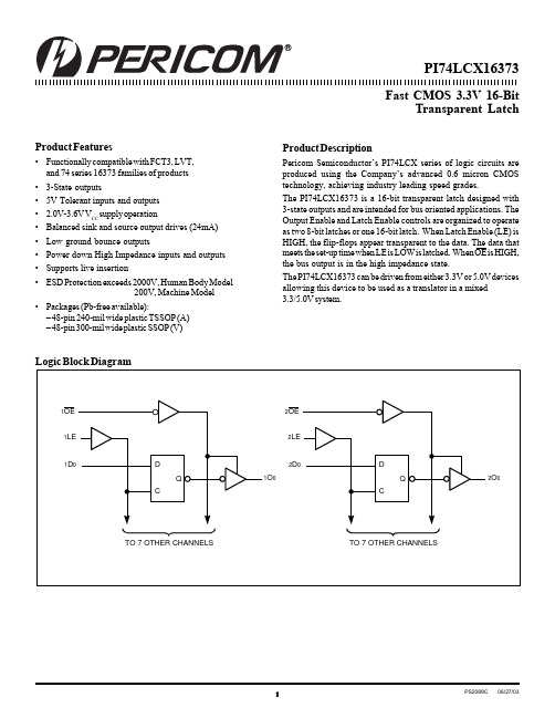
PI74LCX16373 3.3V 16-Bit Transparent Latch 12345678901234567890123456789012123456789012345678901234567890121234567890123456789012345678901212345678901234567890123456789012123456789012
Pin Name xOE
XLE XDX XO X
Truth Table(1)
Inputs ( 1 ) xOE L L H L xLE H H X L xDx H L X X Outputs ( 1 ) xOx H L Z O0
常用电平转化方案
常用的电平转换方案(74HC245、74LVC4245等)(2009-04-04 15:34:54)转载▼标签: 杂谈 分类: 电子世界
1) 晶体管+上拉电阻法
就是一个双极型三极管或 MOSFET,C/D极接一个上拉电阻到正电源,输入电平很灵活,输出电平大致就是正电源电平。
(2) OC/OD 器件+上拉电阻法
跟 1) 类似。适用于器件输出刚好为 OC/OD 的场合。
(3) 74xHCT系列芯片升压 (3.3V→5V)
凡是输入与 5V TTL 电平兼容的 5V CMOS 器件都可以用作 3.3V→5V 电平转换。
——这是由于 3.3V CMOS 的电平刚好和5V TTL电平兼容(巧合),而 CMOS 的输出电平总是接近电源电平的。
(6) 电阻分压法
最简单的降低电平的方法。5V电平,经1.6k+3.3k电阻分压,就是3.3V。
(7) 限流电阻法
如果嫌上面的两个电阻太多,有时还可以只串联一个限流电阻。某些芯片虽然原则上不允许输入电平超过电源,但只要串联一个限流电阻,保证输入保护电流不超过极限(如 74HC 系列为 20mA),仍然是安全的。
例如,74AHC/VHC 系列芯片,其 datasheets 明确注明"输入电压范围为0~5.5V",如果采用 3.3V 供电,就可以实现 5V→3.3V 电平转换。
(5) 专用电平转换芯片
最著名的就是 164245,不仅可以用作升压/降压,而且允许两边电源不同步。这是最通用的电平转换方案,但是也是很昂贵的 (俺前不久买还是¥45/片,虽是零售,也贵的吓人),因此若非必要,最好用前两个方案。
(8) 无为而无不为法
74hc74中文资料
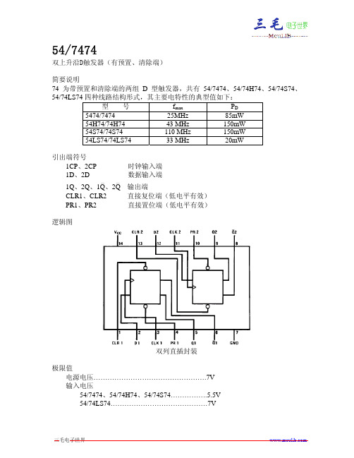
双上升沿D触发器(有预置、清除端)
简要说明
74 为带预置和清除端的两组 D 型触发器,共有 54/7474、54/74H74、54/74S74、
54/74LS74 四种线路结构形式,其主要电特性的典型
5474/7474
25MHz
85mW
54H74/74H74
43 MHz
VI=5.5V(‘LS74 为 PR,CLR
1
1
1
0.2
7V)
IIH 输 入 高 电 平 电 流
Vcc=最大
VIH=2.4V(‘S74 和’LS74 为 2.7V)
D CLR PR CP
40
50
50
120
150
150
80
100
100
80
100
100
20
40 40
uA
20
IIL输入低电平电 流
Vcc=最大 VIL=0.4V(‘S74 为
三毛电子世界
13.5
40
tPLH CP-Q
tPHL
_
CP-Q
25
15
9
25 ns
40
20
9
40
[2]:fmax-最大时钟频率,tPLH输出由低到高传输延迟时间,tPHL输出由高到低传输延迟时间
[3]:测tPHL(PR-Q_ ,CLR-Q),CP(H)时tPHL最大值为 13.5ns,CP(L)时tPHL最大值为 8ns
三毛电子世界
工作环境温度 54XXX …………………………………. -55~125℃ 74XXX …………………………………. 0~70℃
存储温度 ………………………………………….-65~150℃
数管三位电压表电路0-100v

数管三位电压表电路0-100v
数显三位电压表是一种用于测量直流电压的电子仪器,其电路可以实现 0-100V 的电压测量范围,并通过数码管显示测量结果。
以下是一个简单的数显三位电压表电路的设计:
1. 电路原理图
该电路主要由 ADC 转换器、数码管驱动电路、数码管显示电路和电源电路等组成。
- ADC 转换器:采用 ADC0809 芯片,将输入的模拟电压信号转换为数字信号。
- 数码管驱动电路:采用 74HC595 芯片,将 ADC 输出的数字信号转换为数码管显示所需的段码。
- 数码管显示电路:采用三位共阳数码管,显示测量结果。
- 电源电路:采用 LM7805 芯片,将输入的 12V 直流电压转换为 5V 直流电压,为整个电路提供电源。
2. 电路工作原理
当输入电压信号接入电路时,ADC 转换器将模拟电压信号转换为数字信号,并将数字信号输出到数码管驱动电路。
数码管驱动电路将数字信号转换为数码管显示所需的段码,并将段码输出到数码管显示电路。
数码管显示电路根据段码显示测量结果。
3. 电路调试与测试
在电路设计完成后,需要进行调试和测试,以确保电路的正常工作。
可以使用示波器和万用表等仪器对电路进行测试,检查 ADC 转换器的转换精度、数码管的显示效果和电源电路的输出电压等。
以上是一个简单的数显三位电压表电路的设计,仅供参考。
具体的电路设计需要根据实际需求进行调整和优化。
74374中文资料
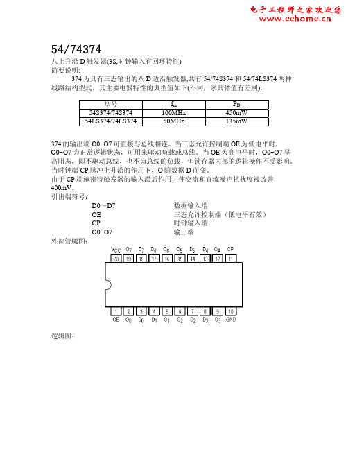
54/74374八上升沿D触发器(3S,时钟输入有回环特性)简要说明:374为具有三态输出的八D边沿触发器,共有54/74S374和54/74LS374两种线路结构型式,其主要电器特性的典型值如下(不同厂家具体值有差别):型号f m P D54S374/74S374 100MHz 450mW54LS374/74LS374 50MHz 135mW374的输出端O0~O7可直接与总线相连。
当三态允许控制端OE为低电平时,O0~O7为正常逻辑状态,可用来驱动负载或总线。
当OE为高电平时,O0~O7呈高阻态,即不驱动总线,也不为总线的负载,但锁存器内部的逻辑操作不受影响。
当时钟端CP脉冲上升沿的作用下,O随数据D而变。
由于CP端施密特触发器的输入滞后作用,使交流和直流噪声抗扰度被改善400mV。
引出端符号:D0~D7 数据输入端OE 三态允许控制端(低电平有效)CP 时钟输入端O0~O7 输出端外部管腿图:逻辑图:真值表:极限值:电源电压 (7V)输入电压5.5V54/74S374…………………………….………….7V 54/74LS374…………………………………….输出高阻态时高电平电压 …………………………. 5.5V工作环境温度54XXX ………………………………….-55~125℃0~70℃74XXX ………………………………….存储温度 …………………………………………. -65~150℃推荐工作条件:54/74374 54/74LS374单位最小额定最大最小额定最大54 4.5 5 5.5 4.5 5 5.5V 电源电压Vcc74 4.75 5 5.25 4.75 5 5.25输入高电平电压V iH 2 2 V54 0.8 0.7V输入低电平电压V iL74 0.8 0.854 -2 -1mA输出高电平电流I OH74 -6.5 -2.654 20 12mA输出低电平电流I OL74 20 24CP(H) 6 15ns脉冲宽度t wCP(L) 7.3 15保持时间t H D 2↓0↓ns建立时间t set D 5↓20↓ns静态特性(TA 为工作环境温度范围)S374 LS374 参 数 测 试 条 件【1】最小 最大 最小 最大单位V IK 输入嵌位电压 Vcc=最小,I ik =-18mA-1.5 -1.5 V V OH 输出高电平电压 Vcc =最小,V IL =最大,V IH =2V ,I OH =最大2.4 2.4 V 54 0.5 0.4 V OL 输出低电平电压 Vcc=最小,V IL =最大,V IH =2V,I OL =最大74 0.5 0.5 V V I =5.5V 1 I I 最大输入电压时输入电流Vcc =最大 V I =7V 0.1 mA V IL =0.5V -0.25 I IL 输入低电平电流 Vcc =最大, V IL =0.4V -0.4mA I IH输入高电平电流 Vcc =最大,V IH =2.7V50 20 uA I OS 输出短路电流 Vcc =最大-40 -100 -30 -130 mA Icc 电源电流 Vcc =最大,OE 接4.5V140 40 mA V 0=2.4V 50 I OZH 输出高阻态时高电平电流 Vcc =最大,V IH =2V V 0=2.7V20 mA V 0=0.5V -50 I OZL 输出高阻态时低电平电流 Vcc =最大,V IH =2V V 0=0.4V-20 mA [1]: 测试条件中的“最小”和“最大”用推荐工作条件中的相应值。
完整word版74HC573功能说明原创编辑
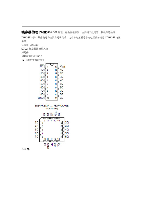
1锁存器的功74CH5774LS37原理一样数据锁存器。
主要用于数码管、按键等等的控74HC57个脚,数据的进和出没有逻辑关系,这个芯片主要是看高电压激活还是274HC57电压激活是低电压激活芯D7D2~脚是数据的输入脚脚是接1脚是高电压激活芯112~1脚是数据的输出是电20121.真值表意思如下:74HC573真值表,1时,输出端数据等于输入端数据;、LE==?第一行/第二行:当OE0 时,输出端保持不变;=、LE0?第三行:当OE=0 为何,输出端为高阻态;Dn、LE 第四行:当OE=1是无论? 2. 高阻态在这种状态下,可以多而是高阻抗的状态;就是输出既不是高电平,也不是低电平,这些芯片中只能有一个处于非高阻态状态,否则会将芯片烧毁。
高个芯片并联输出;但是,通讯中还可以用到。
RS422 阻态的概念在RS232和数据锁存3.数据仍然保持;这个概念在并行数据扩展中当输入的数据消失时,在芯片的输出端, 经常使用到。
4. 数据缓冲加强驱动能力:74LS244/74LS245/74LS373/74LS573都具备数据缓冲的能力。
,输出使能;:output_enable? OE 是锁存的意思;atch:latch_enable,数据锁存使能,LE?路输入数据;:第n ?Dn 路输出数据;On :第n?23在实际应用的时候是这样做的:74HC573波形图,;OE=0a.;先将数据从单片机的口线上输出到Dnb.从0->1->0 ;c.再将LE 这时,你所需要输出的数据就锁存在On上了,输入的数据在变化也影响不到输d.……单出的数据了;实际上,单片机现在在忙着干别的事情,串行通信、扫描键盘片机的资源有限啊。
这条方式进行并行数据的扩展时RAM,使用movx @dptr, A在单片机按照指令时,这些时序是由单片机来实现的。
因为这些参数都是几后面的表格中还有需要时间的参数,你不需要去管它,的情况下,完12M下的每个指令周期最小是1us十ns级别的,对于单片机在全可以实现;如果是你自己来实现这个逻辑,类似的指令如下:MOV P0,A ; //将数据输出到并行数据端口LE CLRSETB LE的波形从LE ; //上面三条指令完成LE0->1->0的变化CLR数据输入和,,74LS37374LS573跟逻辑上完全一样只不过是管脚定义不一样输出端.3。
74HC245详细中文资料

74HC245详细中文资料74HC245是一款高速CMOS器件,74HC2 45引脚兼容低功耗肖特基TTL(LSTTL)系列。
74HC245译码器可接受3位二进制加权地址输入(A0, A1和A2),并当使能时,提供8个互斥的低有效输出(Y0至Y7)。
74HC245特有3个使能输入端:两个低有效(E1和E2)和一个高有效(E3)。
除非E1和E2置低且E3置高,否则74HC138将保持所有输出为高。
利用这种复合使能特性,仅需4片7 4HC245芯片和1个反相器,即可轻松实现并行扩展,组合成为一个1-32(5线到32线)译码器。
任选一个低有效使能输入端作为数据输入,而把其余的使能输入端作为选通端,则74HC245亦可充当一个8输出多路分配器,未使用的使能输入端必须保持绑定在各自合适的高有效或低有效状态。
74HC245与74HC 238逻辑功能一致,只不过74HC138为反相输出。
功能CD74HC245 ,CD74HC238和CD74HCT245, CD74HCT238是高速硅栅CMO S解码器,适合内存地址解码或数据路由应用。
74HC245作用原理于高性能的存贮译码或要求传输延迟时间短的数据传输系统,在高性能存贮器系统中,用这种译码器可以提高译码系统的效率。
将快速赋能电路用于高速存贮器时,译码器的延迟时间和存贮器的赋能时间通常小于存贮器的典型存取时间,这就是说由肖特基钳位的系统译码器所引起的有效系统延迟可以忽略不计。
HC138 按照三位二进制输入码和赋能输入条件,从8 个输出端中译出一个低电平输出。
两个低电平有效的赋能输入端和一个高电平有效的赋能输入端减少了扩展所需要的外接门或倒相器,扩展成24 线译码器不需外接门;扩展成32 线译码器,只需要接一个外接倒相器。
在解调器应用中,赋能输入端可用作数据输入端。
特性复合使能输入,轻松实现扩展兼容JEDEC标准no.7A 存储器芯片译码选择的理想选择低有效互斥输出 ESD保护 HBM EIA/JESD22-A114-C超过2000 V MM EIA/JESD22-A115-A超过200 V 温度范围 -40~+85 ℃ -40~+125 ℃多路分配功能74HC245是一款高速CMOS器件,74HC245引脚兼容低功耗肖特基T TL(LSTTL)系列。
74HC165中文资料
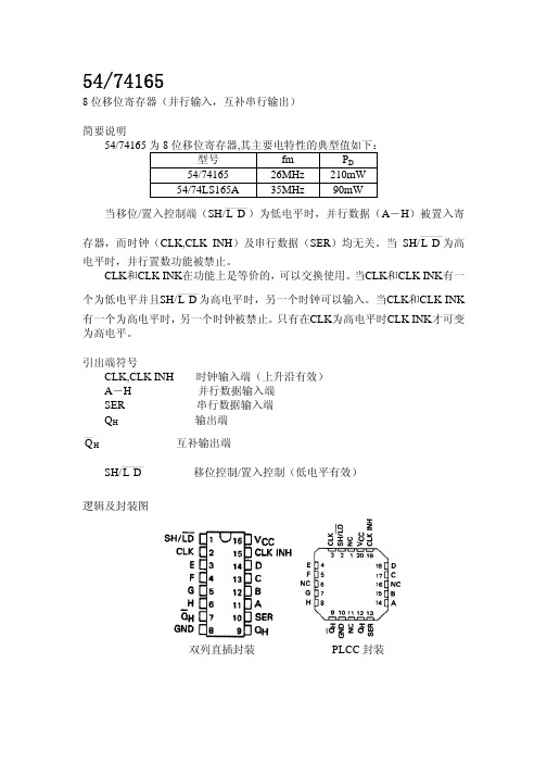
54/741658位移位寄存器(并行输入,互补串行输出)简要说明54/74165为8位移位寄存器,其主要电特性的典型值如下:型号 fmP D210mW54/74165 26MHz54/74LS165A 35MHz 90mW 当移位/置入控制端(SH/L__D__)为低电平时,并行数据(A-H)被置入寄存器,而时钟(CLK,CLK INH)及串行数据(SER)均无关。
当 SH/L__D__为高电平时,并行置数功能被禁止。
CLK和CLK INK在功能上是等价的,可以交换使用。
当CLK和CLK INK有一个为低电平并且SH/L__D__为高电平时,另一个时钟可以输入。
当CLK和CLK INK 有一个为高电平时,另一个时钟被禁止。
只有在CLK为高电平时CLK INK才可变为高电平。
引出端符号CLK,CLK INH 时钟输入端(上升沿有效)A-H 并行数据输入端SER 串行数据输入端Q H输出端Q__H互补输出端SH/L__D__移位控制/置入控制(低电平有效)逻辑及封装图双列直插封装 PLCC封装极限值电源电压 (7V)输入电压………………………………… 5.5VSH/L__D_与CLK INK间电压…………………… 5.5V工作环境温度54164…………………………………… -55~125℃74164…………………………………… -0~70℃储存温度…………………………………… -65℃~150℃真值表H-高电平L-低电平X-任意电平↑-低到高电平跳变时序图推荐工作条件:54/74165最小额定最大单位54 4.555.5电源电压V CC74 4.7555.25V 输入高电平电压V iH 2 V输入低电平电压V iL0.8V 输出高电平电流I OH-400uA 输出低电平电流I OL8mA 时钟频率fcp 0 25MHzCLK 25 ns 脉冲宽度T WL__D_15 nsCLK INK 30 nsA-H 10 nsSER 20 ns 建立时间tsetSH 45 ns 保持时间t H0 ns静态特性(TA为工作环境温度范围)‘165参数测试条件【1】最小最大单位V IK输入嵌位电压 Vcc=最小,V IK=-12mA -1.5 VV OH输出高电平电压Vcc=最小V IH =2V V IL=0.8V, I OH=-800µA2.4 VV OL 输出低电平电压 Vcc=最小,V IH =2V , V IL =0.8V ,I OL =16mA 0.4 V I I 最大输入电压时输入电流 Vcc =最大 V I =5.5V 1 mA SH/L __D _80 I IH 输入高电平电流 其余输入40 µA SH/L __D _ -3.2 I IL 输入低电平电流其余输入Vcc =最大,V IL =0.4V-1.6mA 54 -20 -55 I OS 输出短路电流 Vcc =最大74 -18 -55mA I CC 电源电流Vcc =最大CLK 和CLK INK 接4.5V ,SH/L __D _加脉冲,D 先接4.5V 后接地63 mA[1]: 测试条件中的“最小”和“最大”用推荐工作条件中的相应值。
(完整版)数字电子技术基础习题及答案

数字电子技术基础试题一、填空题 : (每空1分,共10分)1. (30.25) 10 = ( ) 2 = ( ) 16 。
2 . 逻辑函数L = + A+ B+ C +D = 。
3 . 三态门输出的三种状态分别为:、和。
4 . 主从型JK触发器的特性方程= 。
5 . 用4个触发器可以存储位二进制数。
6 . 存储容量为4K×8位的RAM存储器,其地址线为条、数据线为条。
二、选择题: (选择一个正确的答案填入括号内,每题3分,共30分 )1.设图1中所有触发器的初始状态皆为0,找出图中触发器在时钟信号作用下,输出电压波形恒为0的是:()图。
图 12.下列几种TTL电路中,输出端可实现线与功能的电路是()。
A、或非门B、与非门C、异或门D、OC门3.对CMOS与非门电路,其多余输入端正确的处理方法是()。
A、通过大电阻接地(>1.5KΩ)B、悬空C、通过小电阻接地(<1KΩ)D、通过电阻接V CC4.图2所示电路为由555定时器构成的()。
A、施密特触发器B、多谐振荡器C、单稳态触发器D、T触发器5.请判断以下哪个电路不是时序逻辑电路()。
图2A、计数器B、寄存器C、译码器D、触发器6.下列几种A/D转换器中,转换速度最快的是()。
图2A、并行A/D转换器B、计数型A/D转换器C、逐次渐进型A/D转换器D、双积分A/D转换器7.某电路的输入波形 u I 和输出波形 u O 如图 3所示,则该电路为()。
图3A、施密特触发器B、反相器C、单稳态触发器D、JK触发器8.要将方波脉冲的周期扩展10倍,可采用()。
A、10级施密特触发器B、10位二进制计数器C、十进制计数器D、10位D/A转换器9、已知逻辑函数与其相等的函数为()。
A、B、C、D、10、一个数据选择器的地址输入端有3个时,最多可以有()个数据信号输出。
A、4B、6C、8D、16三、逻辑函数化简(每题5分,共10分)1、用代数法化简为最简与或式Y= A +2、用卡诺图法化简为最简或与式Y= + C +A D,约束条件:A C + A CD+AB=0四、分析下列电路。
LT1637 1637FD 微型电源操场类型电阻电压输出电流输入电阻说明书
100µs/DIV1637 TA01b1231637fdInput Offset Voltage Drift (Note 9)N8, S8 Packages, –40°C ≤ T A ≤ 85°C ●13µV/°C MS8 Package, –40°C ≤ T A ≤ 85°C ●26µV/°C DDPackage, –40°C ≤ T A ≤ 85°C ●26µV/°C I OSInput Offset Current●0.4 6.0nA V CM = 44V (Note 5)● 2.5µA I BInput Bias Current●2050nA V CM = 44V (Note 5)●2360µA V S = 0V0.1nA Input Noise Voltage0.1Hz to 10Hz 0.6µV P-P e n Input Noise Voltage Density f = 1kHz 27nV/√Hz i n Input Noise Current Density f = 1kHz0.08pA/√Hz R IN Input Resistance Differential1 2.6M ΩCommon Mode, V CM = 0V to 44V0.7 1.4M ΩC IN Input Capacitance 4pF Input Voltage Range●044V CMRR Common Mode Rejection Ratio V CM = 0V to (V CC – 1V)●88110dB (Note 5)V CM = 0V to 44V (Note 8)●8098dB A VOLLarge-Signal Voltage GainV S = 3V, V O = 500mV to 2.5V, R L = 10k 150400V/mV V S = 3V, 0°C ≤ T A ≤ 70°C ●100V/mV V S = 3V, –40°C ≤ T A ≤ 85°C●75V/mV V S = 5V, V O = 500mV to 4.5V, R L = 10k 300800V/mV V S = 5V, 0°C ≤ T A ≤ 70°C ●200V/mV V S = 5V, –40°C ≤ T A ≤ 85°C●150V/mVV OLOutput Voltage Swing LOWNo Load ●38mV I SINK = 5mA●325700mV V S = 5V, I SINK = 10mA ●5801300mV V OHOutput Voltage Swing HIGHV S = 3V, No Load● 2.94 2.975V V S = 3V, I SOURCE = 5mA ● 2.25 2.67V V S = 5V, No Load● 4.94 4.975V V S = 5V, I SOURCE = 10mA●3.804.45V I SCShort-Circuit Current (Note 2)V S = 3V, Short Output to Ground 1014mA V S = 3V, Short Output to V CC 1545mA V S = 5V, Short Output to Ground 1522mA V S = 5V, Short Output to V CC1560mA PSRRPower Supply Rejection Ratio V S = 3V to 12.5V, V CM = V O = 1V●9098dBMinimum Supply Voltage ● 2.7V Reverse Supply VoltageI S = –100µA●2540V I SSupply Current 190250µA (Note 6)●295µA Supply Current, SHDNV PIN5 = 2V, No Load (Note 6)●312µA I SHDNShutdown Pin CurrentV PIN5 = 0.3V, No Load (Note 6)●0.215nA V PIN5 = 2V, No Load (Note 5)● 1.05µA V PIN5 = 3.3V 2.5µA V PIN5 = 5V4.3µA Output Leakage Current, SHDN V PIN5 = 2V, No Load (Note 6)●0.021µALT1637C/LT1637I SYMBOLPARAMETERCONDITIONSMIN TYP MAXUNITS The ● denotes the specifications which apply over the full operating temperature range of –40°C ≤ T A ≤ 85°C, otherwisespecifications are at T A = 25°C. V S = 3V, 0V; V S = 5V, 0V; V SHDN = V –,V CM = V OUT = half supply unless otherwise specified. (Note 4)3V 5V A D ELECTRICAL CHARACTERISTICS41637fdLT1637C/LT1637I SYMBOL PARAMETER CONDITIONS MIN TYP MAXUNITS V OSInput Offset VoltageN8, S8 Packages 100450µV 0°C ≤ T A ≤ 70°C ●650µV –40°C ≤ T A ≤ 85°C ●800µV MS8 Package 100450µV 0°C ≤ T A ≤ 70°C ●800µV –40°C ≤ T A ≤ 85°C ●1150µV DD Package 125650µV 0°C ≤ T A ≤ 70°C ●1000µV –40°C ≤ T A ≤ 85°C●1150µV Input Offset Voltage Drift (Note 9)N8, S8 Packages, –40°C ≤ T A ≤ 85°C ●13µV/°C MS8 Package, –40°C ≤ T A ≤ 85°C ●26µV/°C DD Package, –40°C ≤ T A ≤ 85°C●26µV/°C I OS Input Offset Current ●16nA I B Input Bias Current ●1750nA Input Noise Voltage 0.1Hz to 10Hz 0.6µV P-P e n Input Noise Voltage Density f = 1kHz 27nV/√Hz i n Input Noise Current Density f = 1kHz0.08pA/√Hz R IN Input Resistance Differential13M ΩCommon Mode, V CM = –15V to 14V2200M ΩC IN Input Capacitance 4pFInput Voltage Range●–1529V CMRR Common Mode Rejection Ratio V CM = –15V to 29V ●80110dB A VOLLarge-Signal Voltage GainV O = ±14V, R L = 10k 100400V/mV 0°C ≤ T A ≤ 70°C ●75V/mV –40°C ≤ T A ≤ 85°C ●50V/mVV OLOutput Voltage Swing LOWNo Load ●–14.997–14.95V I SINK = 5mA ●–14.680–14.25V I SINK = 10mA ●–14.420–13.65VThe ● denotes the specifications which apply over the full operating temperature range of –40°C ≤ T A ≤85°C, otherwise specifications are at T A = 25°C. V S = ±15V, V CM = 0V, V OUT = 0V, V SHDN = V – unless otherwise specified. (Note 4)±15V ELECTRICAL CHARACTERISTICSThe ● denotes the specifications which apply over the full operating temperature range of –40°C ≤ T A ≤85°C, otherwisespecifications are at T A = 25°C. V S = 3V, 0V; V S = 5V, 0V; V SHDN = V –, V CM = V OUT = half supply unless otherwise specified. (Note 4)3V 5V A D ELECTRICAL CHARACTERISTICSLT1637C/LT1637I SYMBOL PARAMETERCONDITIONSMIN TYP MAXUNITS Maximum Shutdown Pin Current V PIN5 = 32V, No Load (Note 5)●20150µA t ON Turn-On Time V PIN5 = 5V to 0V, R L = 10k 45µs t OFF Turn-Off Time V PIN5 = 0V to 5V, R L = 10k 3µs t SETTLING Settling Time0.1% A V = 1, ∆V O = 2V 9µs GBWGain-Bandwidth Product f = 10kHz6501000kHz (Note 5)0°C ≤ T A ≤ 70°C ●550kHz –40°C ≤ T A ≤ 85°C ●500kHz SR Slew Rate A V = –1, R L = ∞0.2100.35V/µs (Note 7)0°C ≤ T A ≤ 70°C ●0.185V/µs –40°C ≤ T A ≤ 85°C●0.170V/µs51637fdV OHOutput Voltage Swing HIGHNo Load●14.914.967V I SOURCE = 5mA ●14.214.667V I SOURCE = 10mA ●13.714.440V I SCShort-Circuit Current (Note 2)Short Output to GND ±25±31.7mA 0°C ≤ T A ≤ 70°C ●±20mA –40°C ≤ T A ≤ 85°C ●±15mA PSRR Power Supply Rejection Ratio V S = ±1.5V to ±22V●90115dBMinimum Supply Voltage ●±1.35V I SSupply Current230300µA ●370µA Positive Supply Current, SHDNV PIN5 = –20V, V S = ±22V, No Load ●640µA I SHDNShutdown Pin Current V PIN5 = –21.7V, V S = ±22V, No Load ●0.315nA V PIN5 = –20V, V S = ±22V, No Load ●0.98µA Maximum Shutdown Pin Current V PIN5 = 32V, V S = ±22V●20150µA Output Leakage Current, SHDNV PIN5 = –20V, V S = ±22V, No Load ●0.022µA V L Shutdown Pin Input Low Voltage V S = ±22V ●–21.7–21.6V V H Shutdown Pin Input High Voltage V S = ±22V●–20.8–20.0V t ON Turn-On Time V PIN5 = –10V to –15V, R L = 10k 35µs t OFF Turn-Off Time V PIN5 = –15V to –10V, R L = 10k 3µs GBWGain-Bandwidth Productf = 10kHz7501100kHz 0°C ≤ T A ≤ 70°C ●650kHz –40°C ≤ T A ≤ 85°C●600kHz SR Slew Rate A V = –1, R L = ∞, V O = ±10V, Measure at V O = ±5V 0.2250.4V/µs 0°C ≤ T A ≤ 70°C ●0.200V/µs –40°C ≤ T A ≤ 85°C●0.180V/µsThe ● denotes the specifications which apply over the full operating temperature range of –40°C ≤ T A ≤85°C, otherwise specifications are at T A = 25°C. V S = ±15V, V CM = 0V, V OUT = 0V, V SHDN = V – unless otherwise specified. (Note 4)LT1637C/LT1637I SYMBOL PARAMETERCONDITIONS MIN TYP MAX UNITS±15V ELECTRICAL CHARACTERISTICS61637fdLT1637H/LT1637MP SYMBOL PARAMETER CONDITIONSMIN TYP MAXUNITS V OSInput Offset Voltage100450µV●3mV Input Offset Voltage Drift (Note 9)●310µV/°C I OS Input Offset Current●15nA V CM = 44V (Note 5)●10µA I BInput Bias Current●150nA V CM = 44V (Note 5)●100µA Input Voltage Range●0.344V CMRR Common Mode Rejection Ratio V CM = 0.3V to (V CC – 1V)●72dB (Note 5)V CM = 0.3V to 44V●74dBA VOLLarge-Signal Voltage GainV S = 3V, V O = 500mV to 2.5V, R L = 10k150400V/mV ●20V/mV V S = 5V, V O = 500mV to 4.5V, R L = 10k300800V/mV ●35V/mVV OLOutput Voltage Swing LOWNo Load ●15mV I SINK = 5mA●900mV V S = 5V, I SINK = 10mA ●1500mV V OHOutput Voltage Swing HIGHV S = 3V, No Load● 2.90V V S = 3V, I SOURCE = 5mA ● 2.05V V S = 5V, No Load● 4.90V V S = 5V, I SOURCE = 10mA● 3.50V PSRR Power Supply Rejection Ratio V S = 3V to 12.5V, V CM = V O = 1V ●80dB Minimum Supply Voltage ●2.7V Reverse Supply VoltageI S = –100µA ●23VI SSupply Current (Note 6)190250µA ●400µA Supply Current, SHDNV PIN5 = 2V, No Load (Note 6)●15µA I SHDNShutdown Pin Current V PIN5 = 0.3V, No Load (Note 6)●200nA V PIN5 = 2V, No Load (Note 5)●7µA Output Leakage Current, SHDN V PIN5 = 2V, No Load (Note 6)●5µA Maximum Shutdown Pin CurrentV PIN5 = 32V, No Load (Note 5)●200µA GBW Gain-Bandwidth Product f = 10kHz (Note 5)6501000kHz ●350kHz SRSlew RateA V = –1, R L = ∞ (Note 7)0.2100.35V/µs ●0.1V/µsThe ● denotes the specifications which apply over the full operating temperature range of –40°C ≤ T A ≤125°C for LT1637H and –55°C ≤ T A ≤ 125°C for LT1637MP. V S = 3V, 0V; V S = 5V, 0V; V CM = V OUT = half supply unless otherwise specified. (Note 4)3V 5V A UD ELECTRICAL CHARACTERISTICSThe ● denotes the specifications which apply over the full operating temperature range of –40°C ≤ T A≤125°C for LT1637H and–55°C ≤ T A≤ 125°C for LT1637MP. V S = ±15V, V CM = 0V, V OUT = 0V, V SHDN = V–, unless otherwise specified. (Note 4)±15V ELECTRICAL CHARACTERISTICSLT1637H/LT1637MPSYMBOL PARAMETER CONDITIONS MIN TYP MAX UNITS V OS Input Offset Voltage100550µV● 3.4mVInput Offset Voltage Drift (Note 9)●311µV/°C I OS Input Offset Current●25nA I B Input Bias Current●250nA CMRR Common Mode Rejection Ratio V CM = –14.7V to 29V●72dBA VOL Large-Signal Voltage Gain V O = ±14V, R L = 10k100400V/mV●4V/mV V O Output Voltage Swing No Load●±14.8VI OUT = ±5mA●±14.0VI OUT= ±10mA●±13.4V PSRR Power Supply Rejection Ratio V S = ±1.5V to 22V●84dB Minimum Supply Voltage●±1.35VI S Supply Current230300µA●500µAPositive Supply Current, SHDN V PIN5 = –20V, V S = ±22V, No Load●60µA I SHDN Shutdown Pin Current V PIN5 = –21.7V, V S = ±22V, No Load●200nAV PIN5 = –20V, V S = ±22V, No Load●10µA Maximum Shutdown Pin Current V PIN5 = 32V, V S = ±22V●200µA Output Leakage Current, SHDN V PIN5 = –20V, V S = ±22V, No Load●100µA V L Shutdown Pin Input Low Voltage V S = ±22V●–21.7V V H Shutdown Pin Input High Voltage V S = ±22V●–20V GBW Gain-Bandwidth Product f = 10kHz7501100kHz●400kHz SR Slew Rate A V = –1, R L = ∞, V O = ±10V,0.2250.4V/µsMeasure at V O = ±5V●0.1V/µsNote 1: Stresses beyond those listed under Absolute Maximum Ratings may cause permanent damage to the device. Exposure to any Absolute Maximum Rating condition for extended periods may affect device reliability and lifetime.Note 2: A heat sink may be required to keep the junction temperature below absolute maximum. The θJA specified for the DD package is with minimal PCB heat spreading metal. Using expanded metal area on all layers of a board reduces this value.Note 3: The LT1637C and LT1637I are guaranteed functional over the operating temperature range of –40°C to 85°C. The LT1637H is guaranteed functional over the operating temperature range of –40°C to 125°C. The LT1637MP is guaranteed functional over the operating temperature range –55°C to 125°C.Note 4: The LT1637C is guaranteed to meet specified performance from 0°C to 70°C. The LT1637C is designed, characterized and expected to meet specified performance from –40°C to 85°C but is not tested or QA sampled at these temperatures. The LT1637I is guaranteed to meet specified performance from –40°C to 85°C. The LT1637H is guaranteed to meet specified performance from –40°C to 125°C and the LT1637MP is guaranteed to meet specified performance from –55°C to 125°C.Note 5: V S = 5V limits are guaranteed by correlation to V S = 3V andV S = ±15V or V S = ±22V tests.Note 6: V S = 3V limits are guaranteed by correlation to V S = 5V andV S = ±15V or V S = ±22V tests.Note 7: Guaranteed by correlation to slew rate at V S = ±15V and GBW at V S = 3V and V S = ±15V tests.Note 8: This specification implies a typical input offset voltage of 650µV at V CM = 44V and a maximum input offset voltage of 5.4mV at V CM = 44V. Note 9: This parameter is not 100% tested.71637fd8TIME (s)081637 G0724619357109100V 10V OUTPUT VOLTAGE (5V/DIV)C1637 G241637 G25A: R L = 2k B: R L = 10k C: R L = 50k1637 G26AB–10V V S = ±15VV S = ±15V A V = –1V S = ±15V A V = 1A B C111637fdSupply VoltageThe positive supply pin of the LT1637 should be bypassed with a small capacitor (about 0.01µF) within an inch of the pin. When driving heavy loads an additional 4.7µF electro-lytic capacitor should be used. When using split supplies,the same is true for the negative supply pin.The LT1637 is protected against reverse battery voltages up to 25V. In the event a reverse battery condition occurs,the supply current is typically less than 1nA.When operating the LT1637 on total supplies of 30V or more, the supply must not be brought up faster than 1µs.This is especially true if low ESR bypass capacitors are used. A series RLC circuit is formed from the supply lead inductance and the bypass capacitor. 5Ω of resistance in the supply or the bypass capacitor will dampen the tuned circuit enough to limit the rise time.InputsThe LT1637 has two input stages, NPN and PNP (see the Simplified Schematic), resulting in three distinct operat-ing regions as shown in the Input Bias Current vs Common Mode typical performance curve.For input voltages about 0.9V or more below V +, the PNP input stage is active and the input bias current is typically –20nA. When the input voltage is about 0.5V or less from V +, the NPN input stage is operating and the input bias current is typically 80nA. Increases in temperature will cause the voltage at which operation switches from the PNP stage to the NPN stage to move towards V +. The input offset voltage of the NPN stage is untrimmed and is typically 600µV.A Schottky diode in the collector of each NPN transistor of the NPN input stage allows the LT1637 to operate with either or both of its inputs above V +. At about 0.3V above V + the NPN input transistor is fully saturated and the input bias current is typically 23µA at room temperature. The input offset voltage is typically 600µV when operating above V +. The LT1637 will operate with its input 44V above V – regardless of V +.APPLICATIO S I FOR ATIOW UUU The inputs are protected against excursions as much as 22V below V – by an internal 1.3k resistor in series with each input and a diode from the input to the negative supply. There is no output phase reversal for inputs up to 5V below V –. There are no clamping diodes between the inputs and the maximum differential input voltage is 44V.OutputThe output voltage swing of the LT1637 is affected by input overdrive as shown in the typical performance curves. When monitoring input voltages within 100mV of V +, gain should be taken to keep the output from clipping.The output of the LT1637 can be pulled up to 25V beyond V + with less than 1nA of leakage current, provided that V +is less than 0.5V.The normally reverse biased substrate diode from the output to V – will cause unlimited currents to flow when the output is forced below V –. If the current is transient and limited to 100mA, no damage will occur.The LT1637 is internally compensated to drive at least 200pF of capacitance under any output loading condi-tions. A 0.22µF capacitor in series with a 150Ω resistor between the output and ground will compensate these amplifiers for larger capacitive loads, up to 4700pF, at all output currents.DistortionThere are two main contributors of distortion in op amps:output crossover distortion as the output transitions from sourcing to sinking current and distortion caused by nonlinear common mode rejection. Of course, if the op amp is operating inverting there is no common mode induced distortion. When the LT1637 switches between input stages there is significant nonlinearity in the CMRR.Lower load resistance increases the output crossover distortion, but has no effect on the input stage transition distortion. For lowest distortion the LT1637 should be operated single supply, with the output always sourcing current and with the input voltage swing between ground and (V + – 0.9V). See the Typical Performance Character-istics curves.121314Information furnished by Linear Technology Corporation is believed to be accurate and reliable. However, no responsibility is assumed for its use. Linear Technology Corporation makes no represen-tation that the interconnection of its circuits as described herein will not infringe on existing patent rights.1516Linear Technology Corporation1630 McCarthy Blvd., Milpitas, CA 95035-7417(408) 432-1900 ● FAX: (408) 434-0507 ● © LINEAR TECHNOLOGY CORPORA TION 2007LT 0107 REV D • PRINTED IN USA。
74HC373

74HC373简介74HC373 是一款高速 CMOS 8 位透明锁存器,适用于数据存储和数据传输应用。
它采用了 CMOS 技术,工作电源范围为2V 至 6V,具有低功耗特性。
74HC373 具有以下特性:•具有 8 位并行数据输入和 8 位并行数据输出端口•可对数据进行锁存,并且锁存的数据可以通过并行输出端口进行读取•提供了 OE (输出使能) 输入端口,可以用来控制并行输出的打开和关闭•具有 3-state 输出,可以通过输出使能端口控制输出的高阻态和有效态之间的切换•提供了 3V 至 6V 的输出电压范围引脚描述74HC373 的引脚描述如下:序号引脚名称描述1OE输出使能输入端口2LE锁存使能输入端口3D0数据输入端口 0 4D1数据输入端口 1 5D2数据输入端口 2 6D3数据输入端口 3 7D4数据输入端口 4 8D5数据输入端口 59D6数据输入端口 6 10D7数据输入端口 7 11GND地12Q0数据输出端口 0 13Q1数据输出端口 1 14Q2数据输出端口 2 15Q3数据输出端口 3 16Q4数据输出端口 4 17Q5数据输出端口 518Q6数据输出端口 619Q7数据输出端口 720VCC电源输入功能描述74HC373 作为一个透明锁存器,可以通过锁存使能输入端口(LE)来控制数据的锁存和透明传输。
当 LE 为高电平时,数据输入端口的数据将被锁存,锁存后的数据可以通过数据输出端口(Q)进行读取。
当 LE 为低电平时,数据输入端口的数据将直接透明传输到数据输出端口。
除了锁存使能输入端口,74HC373 还提供了输出使能输入端口(OE),用于控制输出的打开和关闭。
工作原理74HC373 的工作原理如下:1.当锁存使能输入端口(LE)为高电平时,数据输入端口(D0-D7)的数据将被锁存。
2.锁存的数据可以通过数据输出端口(Q0-Q7)进行读取。
3.当锁存使能输入端口(LE)为低电平时,数据输入端口的数据将直接透明传输到数据输出端口。
74LCX16373G中文资料
© 2005 Fairchild Semiconductor Corporation DS012002February 1994Revised May 200574LCX16373 Low Voltage 16-Bit Transparent Latch with 5V Tolerant Inputs and Outputs74LCX16373Low Voltage 16-Bit Transparent Latch with 5V Tolerant Inputs and OutputsGeneral DescriptionThe LCX16373 contains sixteen non-inverting latches with 3-STATE outputs and is intended for bus oriented applica-tions. The device is byte controlled. The flip-flops appear transparent to the data when the Latch Enable (LE) is HIGH. When LE is LOW, the data that meets the setup time is latched. Data appears on the bus when the Output Enable (OE) is LOW. When OE is HIGH, the outputs are in a high impedance state.The LCX16373 is designed for low voltage (2.5V or 3.3V)V CC applications with capability of interfacing to a 5V signal environment.The LCX16373 is fabricated with an advanced CMOS tech-nology to achieve high speed operation while maintaining CMOS low power dissipation.Featuress 5V tolerant inputs and outputs s 2.3V–3.6V V CC specifications provided s 5.4 ns t PD max (V CC 3.3V), 20 P A I CC max s Power down high impedance inputs and outputs s Supports live insertion/withdrawal (Note 1)s r 24 mA output drive (V CC 3.0V)s Uses patented noise/EMI reduction circuitry s Latch-up performance exceeds 500 mA s ESD performance:Human body model ! 2000V Machine model ! 200Vs Also packaged in plastic Fine-Pitch Ball Grid Array (FBGA)Note 1: To ensure the high-impedance state during power up or down, OE should be tied to V CC through a pull-up resistor: the minimum value or the resistor is determined by the current-sourcing capability of the driver.Ordering Code:Note 2: Ordering code “G ” indicates Trays.Note 3: Devices also available in Tape and Reel. Specify by appending the suffix letter “X ” to the ordering code.Logic SymbolOrder Number Package NumberPackage Description74LCX16373G (Note 2)(Note 3)BGA54A 54-Ball Fine-Pitch Ball Grid Array (FBGA), JEDEC MO-205, 5.5mm Wide 74LCX16373MEA (Note 3)MS48A 48-Lead Small Shrink Outline Package (SSOP), JEDEC MO-118, 0.300" Wide 74LCX16373MTD (Note 3)MTD4848-Lead Thin Shrink Small Outline Package (TSSOP), JEDEC MO-153, 6.1mm Wide 274L C X 16373Connection DiagramsPin Assignment for SSOP and TSSOPPin Assignment for FBGA(Top Thru View)Pin DescriptionsFBGA Pin AssignmentsTruth TablesH HIGH Voltage Level L LOW Voltage Level X ImmaterialZ High ImpedanceO 0 Previous O 0 before HIGH-to-LOW transition of Latch EnablePin Names DescriptionOE n Output Enable Input (Active LOW)LE n Latch Enable Input I 0–I 15Inputs O 0–O 15Outputs NCNo Connect123456A O 0NC OE 1LE 1NC I 0B O 2O 1NC NC I 1I 2C O 4O 3V CC V CC I 3I 4D O 6O 5GND GND I 5I 6E O 8O 7GND GND I 7I 8F O 10O 9GND GND I 9I 10G O 12O 11V CC V CC I 11I 12H O 14O 13NC NC I 13I 14JO 15NCOE 2LE 2NCI 15InputsOutputs LE 1OE 1I 0–I 7O 0–O 7XH X Z H L L L H L H H LL XO 0InputsOutputs LE 2OE 2I 8–I 15O 8–O 15X H X Z H L L L H L H H LLX O 074LCX16373Functional DescriptionThe LCX16373 contains sixteen D-type latches with 3-STATE standard outputs. The device is byte controlled with each byte functioning identically, but independent of the other. Control pins can be shorted together to obtain full 16-bit operation. The following description applies to each byte. When the Latch Enable (LE n ) input is HIGH, data on the I n enters the latches. In this condition the latches are transparent, i.e. a latch output will change state each timeits I input changes. When LE n is LOW, the latches store information that was present on the I inputs a setup time preceding the HIGH-to-LOW transition of LE n . The 3-STATE standard outputs are controlled by the Output Enable (OE n ) input. When OE n is LOW, the standard out-puts are in the 2-state mode. When OE n is HIGH, the stan-dard outputs are in the high impedance mode but this does not interfere with entering new data into the latches.Logic DiagramsPlease note that this diagram is provided only for the understanding of logic operations and should not be used to estimate propagation delays. 474L C X 16373Absolute Maximum Ratings (Note 4)Recommended Operating Conditions (Note 6)Note 4: The Absolute Maximum Ratings are those values beyond which the safety of the device cannot be guaranteed. The device should not be operated at these limits. The parametric values defined in the Electrical Characteristics tables are not guaranteed at the Absolute Maximum Ratings. The “Recom-mended Operating Conditions ” table will define the conditions for actual device operation.Note 5: I O Absolute Maximum Rating must be observed.Note 6: Unused inputs must be held HIGH or LOW. They may not float.DC Electrical CharacteristicsSymbol ParameterValueConditionsUnits V CC Supply Voltage 0.5 to 7.0V V I DC Input Voltage 0.5 to 7.0VV O DC Output Voltage 0.5 to 7.0Output in 3-STATEV 0.5 to V CC 0.5Output in HIGH or LOW State (Note 5)I IK DC Input Diode Current 50V I GND mA I OK DC Output Diode Current 50V O GND mA 50V O ! V CCI O DC Output Source/Sink Current r 50mA I CC DC Supply Current per Supply Pin r 100mA I GND DC Ground Current per Ground Pin r 100mAT STGStorage Temperature65 to 150q CSymbol ParameterMin Max Units V CC Supply Voltage Operating 2.0 3.6V Data Retention1.5 3.6V I Input Voltage 0 5.5V V O Output Voltage HIGH or LOW State0V CC V3-STATE5.5I OH /I OLOutput CurrentV CC 3.0V 3.6V r 24mAV CC 2.7V 3.0V r 12V CC 2.3V 2.7Vr 8T AFree-Air Operating Temperature4085q C 't/'VInput Edge Rate, V IN 0.8V –2.0V, V CC 3.0V10ns/VSymbol ParameterConditionsV CC T A 40q C to 85q C Units (V)Min MaxV IH HIGH Level Input Voltage 2.3 2.7 1.7V 2.7 3.6 2.0V IL LOW Level Input Voltage 2.3 2.70.7V2.73.60.8V OHHIGH Level Output VoltageI OH 100 P A 2.3 3.6V CC 0.2VI OH 8 mA 2.3 1.8I OH 12 mA 2.7 2.2I OH 18 mA 3.0 2.4I OH 24 mA3.0 2.2V OLLOW Level Output VoltageI OL 100 P A 2.3 3.60.2V I OL 8 mA 2.30.6I OL 12 mA 2.70.4I OL 16 mA 3.00.4I OL 24 mA3.00.55I I Input Leakage Current 0 d V I d 5.5V 2.3 3.6r 5.0P A I OZ 3-STATE Output Leakage 0 d V O d 5.5V 2.3 3.6r 5.0P A V I V IH or V IL I OFFPower-Off Leakage CurrentV I or V O 5.5V10P A74LCX16373DC Electrical Characteristics (Continued)Note 7: Outputs disabled or 3-STATE only.AC Electrical CharacteristicsNote 8: Skew is defined as the absolute value of the difference between the actual propagation delay for any two separate outputs of the same device. The specification applies to any outputs switching in the same direction, either HIGH-to-LOW (t OSHL ) or LOW-to-HIGH (t OSLH ). Parameter guaranteed by design.Dynamic Switching CharacteristicsCapacitanceSymbol ParameterConditionsV CC T A 40q C to 85q C Units (V)MinMax I CC Quiescent Supply Current V I V CC or GND2.33.620P A 3.6V d V I , V O d 5.5V (Note 7) 2.3 3.6r 20'I CCIncrease in I CC per InputV IH V CC 0.6V2.33.6500P ASymbolParameterT A 40q C to 85q C, R L 500:UnitsV CC 3.3V r 0.3VV CC 2.7V V CC 2.5V r 0.2VC L 50 pF C L 50 pF C L 30 pF MinMax Min Max Min Max t PHL Propagation Delay 1.5 5.4 1.5 5.9 1.5 6.5ns t PLH I n to O n1.5 5.4 1.5 5.9 1.5 6.5t PHL Propagation Delay 1.5 5.5 1.5 6.4 1.5 6.6ns t PLH LE to O n1.5 5.5 1.5 6.4 1.5 6.6t PZL Output Enable Time1.5 6.1 1.5 6.5 1.57.9ns t PZH 1.5 6.1 1.5 6.5 1.57.9t PLZ Output Disable Time 1.5 6.0 1.5 6.3 1.57.2ns t PHZ 1.5 6.01.5 6.31.57.2t S Setup Time, I n to LE 2.5 2.5 3.0ns t H Hold Time, I n to LE 1.5 1.5 2.0ns t W LE Pulse Width3.03.03.5ns t OSHL Output to Output Skew (Note 8) 1.0ns t OSLH1.0Symbol ParameterConditionsV CC T A 25q C Units (V)Typical V OLP Quiet Output Dynamic Peak V OL C L 50 pF, V IH 3.3V, V IL 0V 3.30.8V C L 30 pF, V IH 2.5V, V IL 0V 2.50.6V OLVQuiet Output Dynamic Valley V OLC L 50 pF, V IH 3.3V, V IL 0V 3.3 0.8VC L 30 pF, V IH 2.5V, V IL 0V2.50.6Symbol ParameterConditionsTypical Units C IN Input Capacitance V CC Open, V I 0V or V CC 7pF C OUT Output CapacitanceV CC 3.3V, V I 0V or V CC8pF C PDPower Dissipation CapacitanceV CC 3.3V, V I 0V or V CC , f 10 MHz20pF 674L C X 16373AC LOADING and WAVEFORMS Generic for LCX FamilyFIGURE 1. AC Test Circuit (C L includes probe and jig capacitance)Waveform for Inverting and Non-Inverting FunctionsPropagation Delay. Pulse Width and t rec Waveforms3-STATE Output Low Enable andDisable Times for Logic3-STATE Output High Enable andDisable Times for LogicSetup Time, Hold Time and Recovery Time for Logict rise and t fallFIGURE 2. Waveforms(Input Characteristics; f =1MHz, t r = t f = 3ns)Test Switch t PLH , t PHL Opent PZL , t PLZ 6V at V CC 3.3 r 0.3V, and 2.7V V CC x 2 at V CC 2.5 r 0.2Vt PZH , t PHZGNDSymbol V CC3.3V r 0.3V2.7V 2.5V r 0.2V V mi 1.5V 1.5V V CC /2V mo 1.5V 1.5V V CC /2V x V OL 0.3V V OL 0.3V V OL 0.15V V yV OH 0.3VV OH 0.3VV OH 0.15V74LCX16373 Schematic DiagramGeneric for LCX Family 874L C X 16373Physical Dimensionsinches (millimeters) unless otherwise noted54-Ball Fine-Pitch Ball Grid Array (FBGA), JEDEC MO-205, 5.5mm WidePackage Number BGA54A74LCX16373 Physical Dimensions inches (millimeters) unless otherwise noted (Continued)48-Lead Small Shrink Outline Package (SSOP), JEDEC MO-118, 0.300" WidePackage Number MS48A1074L C X 16373 L o w V o l t a g e 16-B i t T r a n s p a r e n t L a t c h w i t h 5V T o l e r a n t I n p u t s a n d O u t p u t sPhysical Dimensions inches (millimeters) unless otherwise noted (Continued)48-Lead Thin Shrink Small Outline Package (TSSOP), JEDEC MO-153, 6.1mm WidePackage Number MTD48Fairchild does not assume any responsibility for use of any circuitry described, no circuit patent licenses are implied and Fairchild reserves the right at any time without notice to change said circuitry and specifications.LIFE SUPPORT POLICYFAIRCHILD ’S PRODUCTS ARE NOT AUTHORIZED FOR USE AS CRITICAL COMPONENTS IN LIFE SUPPORT DEVICES OR SYSTEMS WITHOUT THE EXPRESS WRITTEN APPROVAL OF THE PRESIDENT OF FAIRCHILD SEMICONDUCTOR CORPORATION. As used herein:1.Life support devices or systems are devices or systems which, (a) are intended for surgical implant into the body, or (b) support or sustain life, and (c) whose failure to perform when properly used in accordance with instructions for use provided in the labeling, can be rea-sonably expected to result in a significant injury to the user. 2. A critical component in any component of a life support device or system whose failure to perform can be rea-sonably expected to cause the failure of the life support device or system, or to affect its safety or effectiveness.。
74ls373中文资料
型号
tPd
54S373/74S373
7ns
54LS373/74LS373
17ns
PD 525mW 120mW
373 的输出端 O0~O7 可直接与总线相连。
当三态允许控制端 OE 为低电平时,O0~O7 为正常逻辑状态,可用来驱动负载或总
线。当 OE 为高电平时,O0~O7 呈高阻态,即不驱动总线,也不为总线的负载,但
ic中文-17IC中文资料网 - IC中文资料-IC渠道网 IC中文资料 - 电源 - 嵌入式 - 电路图 - 单片机 - 应用方案 - 技术文章
首 页 IC库存 电子资讯 技术资料
IC
非IC
求购信息
PDF 资料
IC库存搜索: 请输入IC型号
搜索
最新搜索: VN2406LZL1 MAX881REUB+T IC42S16400-6TG LTC2230IUP MSR320 HLMP-2700 GS-R405S EPF10K10LI84 …
IC中文资料
型号A开头
型号B 开头
型号C开头
·MCP1316中文资料MCP1317应用MCP1318 MCP1319封装图MC... ·MCP111 中文资料 MCP112 应用 pdf 封装图 管脚说明... ·MCP102中文资料MCP103应用MCP111 MCP121封装图MCP131... ·MCP41010 中文资料 MCP41050 应用 pdf MCP41100 封... ·MCP40D17中文资料 MCP40D18应用 pdf MCP40D19 封装图... ·DS12R885 中文资料 DS12CR887 应用 pdf DS12R887封... ·MAX6972ATJ 中文资料 MAX6973ATJ 应用 pdf 封装图 管脚... ·MCP14E3中文资料MCP14E4 应用 pdf 封装图 MCP14E5管脚说... ·MCP6V06中文资料 MCP6V07应用 pdf 封装图 MCP6V08管脚说... ·MCP6V01中文资料MCP6V02应用 pdf 封装图MCP6V03 管脚说明...
74ls373和74hc573有什么区别
74ls373和74hc573有什么区别74ls373和74hc573都是八D锁存器(三态)。
74ls373是TTL电路,电源电压是5V。
74hc573是cmos电路,电源电压工作范围是2V ~ 6V。
74ls373和74hc573的引脚编排不一样。
一、锁存器74hc57374HC573是拥有八路输出的透明锁存器,输出为三态门,是一种高性能硅栅CMOS器件。
SL74HC573跟LS/AL573的管脚一样。
器件的输入是和标准CMOS 输出兼容的,加上拉电阻他们能和LS/ALSTTL输出兼容。
当锁存使能端LE为高时,这些器件的锁存对于数据是透明的(也就是说输出同步)。
当锁存使能变低时,符合建立时间和保持时间的数据会被锁存。
I/O输出能直接接到CMOS,NMOS 和TTL 接口上工作电压范围:2.0V~6.0V最低输入电流:1.0uA器件的高噪声抵抗特性三态总线驱动输出置数全并行存取缓冲控制输入使能输入有改善抗扰度的滞后作用编程时:1.使能端置1,此时输出数据和输入数据一致;2.使能端清0,输出端保持原有值,使得输出的数据锁定,防止误操作。
真值表及功能:二、74ls37374LS373是一款常用的地址锁存器芯片,由八个并行的、带三态缓冲输出的D 触发器构成。
在单片机系统中为了扩展外部存储器,通常需要一块74LS373芯片。
(1).1脚是输出使能(OE),是低电平有效,当1脚是高电平时,不管输入3、4、7、8、13、14、17、18如何,也不管11脚(锁存控制端,G)如何,输出2(Q0)、5(Q1)、6(Q2)、9(Q3)、12(Q4)、15(Q5)、16(Q6)、19(Q7)全部呈现高阻状态(或者叫。
74ls373
74LS373中文资料2010年12月13日星期一 17:1254/74373八D锁存器(3S,锁存允许输入有回环特性)简要说明:373为三态输出的八D透明锁存器,共有54/74S373和54/74LS373两种线路结构型式。
373为三态输出的8 D透明锁存器, 373的输出端O0-O7可直接与总线相连。
当三态允许控制端OE为低电平时,O0-O7为正常逻辑状态,可用来驱动负载或总线。
当OE为高电平时,O0-O7呈高阻态,即不驱动总线,也不为总线的负载,但锁存器内部的逻辑操作不受影响。
当锁存允许端LE为高电平时,O 随数据D而变。
当LE为低电平时,O被锁存在已建立的数据电平。
当LE端施密特触发器的输入滞后作用,使交流和直流噪声抗扰度被改善400mV。
373引出端符号:D0~D7-----数据输入端 OE-----三态允许控制端(低电平有效)LE-----锁存允许端 O0-O7-----输出端373外部管腿图、真值表:(1).1脚是输出使能(OE),是低电平有效,当1脚是高电平时,不管输入3、4、7、8、13、14、17、18如何,也不管11脚(锁存控制端,G)如何,输出2(Q0)、5(Q1)、6(Q2)、9(Q3)、12(Q4)、15(Q5)、16(Q6)、19(Q7)全部呈现高阻状态(或者叫浮空状态);(2).当1脚是低电平时,只要11脚(锁存控制端,G)上出现一个下降沿,输出2(Q 0)、5(Q1)、6(Q2)、9(Q3)、12(Q4)、15(Q5)、16(Q6)、19(Q7)立即呈现输入脚3、4、7、8、13、14、17、18的状态.锁存端LE 由高变低时,输出端8 位信息被锁存,直到LE 端再次有效。
当三态门使能信号OE为低电平时,三态门导通,允许Q0~Q7输出,OE为高电平时,输出悬空。
当74LS373用作地址锁存器时,应使OE为低电平,此时锁存使能端C为高电平时,输出Q0~Q7 状态与输入端D1~D7状态相同;当C发生负的跳变时,输入端D0~D7 数据锁入Q0~Q7。
74hc74的中文资料

D(L) 20*
保持时间tH
5*
*表示以 CP 上升沿为参考
54H74/74H74 最小 额定 最大
4.5
5
5.5
4.75 5 5.25
2
0.8
0.8
-1000
20 20
0
35
15 13.5 25
10* 15*
5*
54S74/74S74 最小 额定 最大
4.5 5
5.5
4.75 5
5.25
2 0.8
0.5V)
D CLR PR CP
-1.6
-2
-3.2
-4
-1.6
-2
-3.2
-4
-2
-0.4
-6 -4
-0.8 -0.8
mA
-4
-0.4
IOS输出短路电流
Vcc=最大
54 74
-20 -18
-57 -57
-40 -40
-100 -100
-40 -40
-100 -100
-20 -20
-100 -100
VI=5.5V(‘LS74 为 PR,CLR
1
1
1
0.2
7V)
IIH 输 入 高 电 平 电 流
Vcc=最大
VIH=2.4V(‘S74 和’LS74 为 2.7V)
D CLR PR CP
40
50
50
120
150
150
80
100
100
80
100
100
20
40 40
uA
20
IIL输入低电平电 流
Vcc=最大 VIL=0.4V(‘S74 为
数字电子技术_三江学院中国大学mooc课后章节答案期末考试题库2023年
数字电子技术_三江学院中国大学mooc课后章节答案期末考试题库2023年1.触发器是一种()。
答案:双稳态电路2.二输入与非门中,一个输入端接高电平1,另外一个输入端接方波信号,则输出应为()。
答案:与输入方波信号反相3.以下常用于总线应用的是()。
答案:三态门4.下列关于多余输入端的处理的描述,正确的是()答案:与门和与非门的多余输入端可以接高电平5.以下不属于组合逻辑电路的是()。
答案:计数器6.二-十进制编码器的输入编码信号应有()个。
答案:107.15的8421BCD码是()答案:000101018.下列说法错误的是()。
答案:CMOS门电路的优点是静态功耗小、噪声容限低,输入电阻高。
9.将边沿D触发器的端与D端相连,则触发器Q端输出脉冲的频率为时钟脉冲CP的( )。
答案:1/210.由两个模数分别为M和N的计数器级联成的计数器,其最大模数为( ).答案:M*N11.一个三进制计数器和一个八进制计数器串接起来后的最大计数值是( ).答案:2412.利用集成计数器的同步置数功能构成N进制计数器时,写二进制代码的数是( ).答案:N-113.利用集成计数器的异步清零功能构成N进制计数器时,写二进制代码的数是( ).答案:N14.由4个触发器构成的计数器,状态利用率最高的是( ).答案:二进制计数器15.在由双向移位寄存器74LS194组成的扭环形计数器中,若4位(1~4)移位寄存器的第3个输出端通过非门加到串行数码输入端上,则可构成( )分频电路。
答案:616.倒T型电阻网络DA转换器中,电阻网络中的电阻值只有R、2R两种,各节点对地的等效电阻均为()。
答案:R17.在AD转换器中,量化单位是指数字信号最低位为()时所对应的模拟电压。
答案:118.AD转换中,取样脉冲的频率应大于等于输入模拟信号频谱中最高频率的()倍。
答案:219.R-2R电阻网络DA转换器中的阻值为()。
答案:R和2R20.具有N个输出端的译码器,其输入信号应该至少是()位。
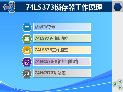
二74LS373引脚功能74LS373锁存器工作原理5
74LS373锁存器工作原理 3
二 74LS373引脚功能
74LS373是数据锁存器,锁存器大大缓解处理器的压力,主要用于 解决驱动及扩展问题,它与74HC573功能基本一致。
OUTPUT ENABLE: 三态允许控制端
当锁存允许端 LE 为高电平时,O 随数据 D 而变。当 LE 为低电平时, Q被锁存在已建立的数据电平。当LE端施密特触发器的输入滞后作用, 使交流和直流噪声抗扰度被改善 400mV。
74LS373锁存器工作原理 5
四 74HC573逻辑控制电路
74LS373锁存器工作原理 6
五 74HC573功能表
D0~D7:数 据输入引脚Leabharlann Q0~Q7:数 据输出引脚
CLOCK:存储 使能端
74LS373锁存器工作原理 4
三 74LS373工作原理
当三态允许控制端 OE 为低 电平时,Q0~Q7 为正常逻 辑状态,可用来驱动负载或 总线。当 OE 为高电平时, Q0~Q7 呈高阻态,即不驱 动总线,也不为总线的负载, 但锁存器内部的逻辑操作不 受影响。
输出控制 G D
1
0
1
0
0
0x
1
xx
输出 1 0 Qn
高阻
74LS373锁存器工作原理 1
一 认识锁存器 二 74LS373引脚功能 三 74LS373工作原理 四 74HC573逻辑控制电路 五 74HC573功能表
74LS373锁存器工作原理 2
一 认识锁存器
锁存器:由若干个电平触发的D触发器构成的一次能存储多位二进制 代码的时序逻辑电路,叫作锁存器。
74123中文资料
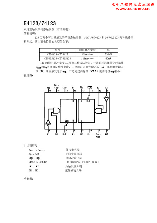
【4】 :tPLH-输出由低到高电平传输延迟时间 tPHL-输出由高到低电平传输延迟时间 tWQ-Q 端输出脉冲宽度
外接电容端 正脉冲输出端 负脉冲输出端 直接清除端(低电平有效) 负触发输入端 正触发输入端
说明:1.外接电容接在 Cext(正)和 Rext/Cext(正)之间 2.为了改善脉冲宽度的精度和重复性,可在 Rext/Cext 和 Vcc 之间接外接电阻。 3.为了得到可变脉冲宽度,可在 Rext/Cext 和 Vcc 之间接 接可变电阻。 H-高电平 L-低电平 X-任意 ↑-低到高电平跳变 ↓-高到低电平跳变 -一个高电平脉冲 -一个低电平脉冲 极限值 电源电压------------------------------------------------7V 输入电压 54/74123-----------------------------------------5.5V 54/74LS123--------------------------------------7V 工作环境温度 54×××------------------------------ -55~125℃ 74×××------------------------------------0~70℃ 贮存温度-------------------------------------- -65~150℃ 逻辑图(1/2)
54 74 54 74
2.4 2.4 0.4 0.4 1 40 80 -1.6
2.5 V 2.7 0.4 0.5 0.1 20 20 -0.4 mA -3.2 -0.4 -20 -100 20 mA mA mA μA V
VOL 输出低电平电压 II 最大输入电压时输入电流 IIH 输入高 电平电流 VIH 输 入 低电平电 流 CLR IOS 输出短路电流 Icc 电源电流 A,B CLR A,B
74573引脚图

8D数据锁存器和373一样
74573引脚图
三态总线驱动输出
·置数全并行存取
·缓冲控制输入
·使能输入有改善抗扰度的滞后作用
原理:74LS573 的八个锁存器都是透明的D 型锁存器,当使能(G)为高时,Q 输出将随数据(D)输入而变。
当使能为低时,输出将锁存在已建立的数据电平上。
输出控制不影响锁存器的内部工作,即老数据可以保持,甚至当输出被关闭时,新的数据也可以置入。
这种电路可以驱动大电容或低阻抗负载,可以直接与系统总线接口并驱动总线,而不需要外接口。
特别适用于缓冲寄存器,I/O 通道,双向总线驱动器和工作寄存器。
真值表:
输出enable
Latch
ENABLE启
用
D
输出
O
L H H H L H L L L L X QO H X X Z
H=高电平 L=低电平×=不定 Z=高阻态QO=建立稳态输入条件前Q的电平
引脚功能表:
Operating Conditions 操作条件。
- 1、下载文档前请自行甄别文档内容的完整性,平台不提供额外的编辑、内容补充、找答案等附加服务。
- 2、"仅部分预览"的文档,不可在线预览部分如存在完整性等问题,可反馈申请退款(可完整预览的文档不适用该条件!)。
- 3、如文档侵犯您的权益,请联系客服反馈,我们会尽快为您处理(人工客服工作时间:9:00-18:30)。
© 2005 Fairchild Semiconductor Corporation DS012002February 1994Revised May 200574LCX16373 Low Voltage 16-Bit Transparent Latch with 5V Tolerant Inputs and Outputs74LCX16373Low Voltage 16-Bit Transparent Latch with 5V Tolerant Inputs and OutputsGeneral DescriptionThe LCX16373 contains sixteen non-inverting latches with 3-STATE outputs and is intended for bus oriented applica-tions. The device is byte controlled. The flip-flops appear transparent to the data when the Latch Enable (LE) is HIGH. When LE is LOW, the data that meets the setup time is latched. Data appears on the bus when the Output Enable (OE) is LOW. When OE is HIGH, the outputs are in a high impedance state.The LCX16373 is designed for low voltage (2.5V or 3.3V)V CC applications with capability of interfacing to a 5V signal environment.The LCX16373 is fabricated with an advanced CMOS tech-nology to achieve high speed operation while maintaining CMOS low power dissipation.Featuress 5V tolerant inputs and outputs s 2.3V–3.6V V CC specifications provided s 5.4 ns t PD max (V CC 3.3V), 20 P A I CC max s Power down high impedance inputs and outputs s Supports live insertion/withdrawal (Note 1)s r 24 mA output drive (V CC 3.0V)s Uses patented noise/EMI reduction circuitry s Latch-up performance exceeds 500 mA s ESD performance:Human body model ! 2000V Machine model ! 200Vs Also packaged in plastic Fine-Pitch Ball Grid Array (FBGA)Note 1: To ensure the high-impedance state during power up or down, OE should be tied to V CC through a pull-up resistor: the minimum value or the resistor is determined by the current-sourcing capability of the driver.Ordering Code:Note 2: Ordering code “G ” indicates Trays.Note 3: Devices also available in Tape and Reel. Specify by appending the suffix letter “X ” to the ordering code.Logic SymbolOrder Number Package NumberPackage Description74LCX16373G (Note 2)(Note 3)BGA54A 54-Ball Fine-Pitch Ball Grid Array (FBGA), JEDEC MO-205, 5.5mm Wide 74LCX16373MEA (Note 3)MS48A 48-Lead Small Shrink Outline Package (SSOP), JEDEC MO-118, 0.300" Wide 74LCX16373MTD (Note 3)MTD4848-Lead Thin Shrink Small Outline Package (TSSOP), JEDEC MO-153, 6.1mm Wide 274L C X 16373Connection DiagramsPin Assignment for SSOP and TSSOPPin Assignment for FBGA(Top Thru View)Pin DescriptionsFBGA Pin AssignmentsTruth TablesH HIGH Voltage Level L LOW Voltage Level X ImmaterialZ High ImpedanceO 0 Previous O 0 before HIGH-to-LOW transition of Latch EnablePin Names DescriptionOE n Output Enable Input (Active LOW)LE n Latch Enable Input I 0–I 15Inputs O 0–O 15Outputs NCNo Connect123456A O 0NC OE 1LE 1NC I 0B O 2O 1NC NC I 1I 2C O 4O 3V CC V CC I 3I 4D O 6O 5GND GND I 5I 6E O 8O 7GND GND I 7I 8F O 10O 9GND GND I 9I 10G O 12O 11V CC V CC I 11I 12H O 14O 13NC NC I 13I 14JO 15NCOE 2LE 2NCI 15InputsOutputs LE 1OE 1I 0–I 7O 0–O 7XH X Z H L L L H L H H LL XO 0InputsOutputs LE 2OE 2I 8–I 15O 8–O 15X H X Z H L L L H L H H LLX O 074LCX16373Functional DescriptionThe LCX16373 contains sixteen D-type latches with 3-STATE standard outputs. The device is byte controlled with each byte functioning identically, but independent of the other. Control pins can be shorted together to obtain full 16-bit operation. The following description applies to each byte. When the Latch Enable (LE n ) input is HIGH, data on the I n enters the latches. In this condition the latches are transparent, i.e. a latch output will change state each timeits I input changes. When LE n is LOW, the latches store information that was present on the I inputs a setup time preceding the HIGH-to-LOW transition of LE n . The 3-STATE standard outputs are controlled by the Output Enable (OE n ) input. When OE n is LOW, the standard out-puts are in the 2-state mode. When OE n is HIGH, the stan-dard outputs are in the high impedance mode but this does not interfere with entering new data into the latches.Logic DiagramsPlease note that this diagram is provided only for the understanding of logic operations and should not be used to estimate propagation delays. 474L C X 16373Absolute Maximum Ratings (Note 4)Recommended Operating Conditions (Note 6)Note 4: The Absolute Maximum Ratings are those values beyond which the safety of the device cannot be guaranteed. The device should not be operated at these limits. The parametric values defined in the Electrical Characteristics tables are not guaranteed at the Absolute Maximum Ratings. The “Recom-mended Operating Conditions ” table will define the conditions for actual device operation.Note 5: I O Absolute Maximum Rating must be observed.Note 6: Unused inputs must be held HIGH or LOW. They may not float.DC Electrical CharacteristicsSymbol ParameterValueConditionsUnits V CC Supply Voltage 0.5 to 7.0V V I DC Input Voltage 0.5 to 7.0VV O DC Output Voltage 0.5 to 7.0Output in 3-STATEV 0.5 to V CC 0.5Output in HIGH or LOW State (Note 5)I IK DC Input Diode Current 50V I GND mA I OK DC Output Diode Current 50V O GND mA 50V O ! V CCI O DC Output Source/Sink Current r 50mA I CC DC Supply Current per Supply Pin r 100mA I GND DC Ground Current per Ground Pin r 100mAT STGStorage Temperature65 to 150q CSymbol ParameterMin Max Units V CC Supply Voltage Operating 2.0 3.6V Data Retention1.5 3.6V I Input Voltage 0 5.5V V O Output Voltage HIGH or LOW State0V CC V3-STATE5.5I OH /I OLOutput CurrentV CC 3.0V 3.6V r 24mAV CC 2.7V 3.0V r 12V CC 2.3V 2.7Vr 8T AFree-Air Operating Temperature4085q C 't/'VInput Edge Rate, V IN 0.8V –2.0V, V CC 3.0V10ns/VSymbol ParameterConditionsV CC T A 40q C to 85q C Units (V)Min MaxV IH HIGH Level Input Voltage 2.3 2.7 1.7V 2.7 3.6 2.0V IL LOW Level Input Voltage 2.3 2.70.7V2.73.60.8V OHHIGH Level Output VoltageI OH 100 P A 2.3 3.6V CC 0.2VI OH 8 mA 2.3 1.8I OH 12 mA 2.7 2.2I OH 18 mA 3.0 2.4I OH 24 mA3.0 2.2V OLLOW Level Output VoltageI OL 100 P A 2.3 3.60.2V I OL 8 mA 2.30.6I OL 12 mA 2.70.4I OL 16 mA 3.00.4I OL 24 mA3.00.55I I Input Leakage Current 0 d V I d 5.5V 2.3 3.6r 5.0P A I OZ 3-STATE Output Leakage 0 d V O d 5.5V 2.3 3.6r 5.0P A V I V IH or V IL I OFFPower-Off Leakage CurrentV I or V O 5.5V10P A74LCX16373DC Electrical Characteristics (Continued)Note 7: Outputs disabled or 3-STATE only.AC Electrical CharacteristicsNote 8: Skew is defined as the absolute value of the difference between the actual propagation delay for any two separate outputs of the same device. The specification applies to any outputs switching in the same direction, either HIGH-to-LOW (t OSHL ) or LOW-to-HIGH (t OSLH ). Parameter guaranteed by design.Dynamic Switching CharacteristicsCapacitanceSymbol ParameterConditionsV CC T A 40q C to 85q C Units (V)MinMax I CC Quiescent Supply Current V I V CC or GND2.33.620P A 3.6V d V I , V O d 5.5V (Note 7) 2.3 3.6r 20'I CCIncrease in I CC per InputV IH V CC 0.6V2.33.6500P ASymbolParameterT A 40q C to 85q C, R L 500:UnitsV CC 3.3V r 0.3VV CC 2.7V V CC 2.5V r 0.2VC L 50 pF C L 50 pF C L 30 pF MinMax Min Max Min Max t PHL Propagation Delay 1.5 5.4 1.5 5.9 1.5 6.5ns t PLH I n to O n1.5 5.4 1.5 5.9 1.5 6.5t PHL Propagation Delay 1.5 5.5 1.5 6.4 1.5 6.6ns t PLH LE to O n1.5 5.5 1.5 6.4 1.5 6.6t PZL Output Enable Time1.5 6.1 1.5 6.5 1.57.9ns t PZH 1.5 6.1 1.5 6.5 1.57.9t PLZ Output Disable Time 1.5 6.0 1.5 6.3 1.57.2ns t PHZ 1.5 6.01.5 6.31.57.2t S Setup Time, I n to LE 2.5 2.5 3.0ns t H Hold Time, I n to LE 1.5 1.5 2.0ns t W LE Pulse Width3.03.03.5ns t OSHL Output to Output Skew (Note 8) 1.0ns t OSLH1.0Symbol ParameterConditionsV CC T A 25q C Units (V)Typical V OLP Quiet Output Dynamic Peak V OL C L 50 pF, V IH 3.3V, V IL 0V 3.30.8V C L 30 pF, V IH 2.5V, V IL 0V 2.50.6V OLVQuiet Output Dynamic Valley V OLC L 50 pF, V IH 3.3V, V IL 0V 3.3 0.8VC L 30 pF, V IH 2.5V, V IL 0V2.50.6Symbol ParameterConditionsTypical Units C IN Input Capacitance V CC Open, V I 0V or V CC 7pF C OUT Output CapacitanceV CC 3.3V, V I 0V or V CC8pF C PDPower Dissipation CapacitanceV CC 3.3V, V I 0V or V CC , f 10 MHz20pF 674L C X 16373AC LOADING and WAVEFORMS Generic for LCX FamilyFIGURE 1. AC Test Circuit (C L includes probe and jig capacitance)Waveform for Inverting and Non-Inverting FunctionsPropagation Delay. Pulse Width and t rec Waveforms3-STATE Output Low Enable andDisable Times for Logic3-STATE Output High Enable andDisable Times for LogicSetup Time, Hold Time and Recovery Time for Logict rise and t fallFIGURE 2. Waveforms(Input Characteristics; f =1MHz, t r = t f = 3ns)Test Switch t PLH , t PHL Opent PZL , t PLZ 6V at V CC 3.3 r 0.3V, and 2.7V V CC x 2 at V CC 2.5 r 0.2Vt PZH , t PHZGNDSymbol V CC3.3V r 0.3V2.7V 2.5V r 0.2V V mi 1.5V 1.5V V CC /2V mo 1.5V 1.5V V CC /2V x V OL 0.3V V OL 0.3V V OL 0.15V V yV OH 0.3VV OH 0.3VV OH 0.15V 74LCX16373Schematic DiagramGeneric for LCX Family 874L C X 16373Physical Dimensionsinches (millimeters) unless otherwise noted54-Ball Fine-Pitch Ball Grid Array (FBGA), JEDEC MO-205, 5.5mm WidePackage Number BGA54A 74LCX16373Physical Dimensions inches (millimeters) unless otherwise noted (Continued)48-Lead Small Shrink Outline Package (SSOP), JEDEC MO-118, 0.300" WidePackage Number MS48A1074L C X 16373 L o w V o l t a g e 16-B i t T r a n s p a r e n t L a t c h w i t h 5V T o l e r a n t I n p u t s a n d O u t p u t sPhysical Dimensions inches (millimeters) unless otherwise noted (Continued)48-Lead Thin Shrink Small Outline Package (TSSOP), JEDEC MO-153, 6.1mm WidePackage Number MTD48Fairchild does not assume any responsibility for use of any circuitry described, no circuit patent licenses are implied and Fairchild reserves the right at any time without notice to change said circuitry and specifications.LIFE SUPPORT POLICYFAIRCHILD ’S PRODUCTS ARE NOT AUTHORIZED FOR USE AS CRITICAL COMPONENTS IN LIFE SUPPORT DEVICES OR SYSTEMS WITHOUT THE EXPRESS WRITTEN APPROVAL OF THE PRESIDENT OF FAIRCHILD SEMICONDUCTOR CORPORATION. As used herein:1.Life support devices or systems are devices or systems which, (a) are intended for surgical implant into the body, or (b) support or sustain life, and (c) whose failure to perform when properly used in accordance with instructions for use provided in the labeling, can be rea-sonably expected to result in a significant injury to the user. 2. A critical component in any component of a life support device or system whose failure to perform can be rea-sonably expected to cause the failure of the life support device or system, or to affect its safety or effectiveness.。