呼吸机专用mos管 AP15P06D -15A -60V TO-252
呼吸机专用mos管 AP20N03D 20A 30V TO-252
1The AP20N03D uses advanced trench technology to provide excellent R DS(ON), low gate charge and operation with gate voltages as low as 4.5V. This device is suitable for use as aBattery protection or in other Switching application.V DS = 30V I D =20AR DS(ON) < 25m Ω@ V GS =10VBattery protection Load switchUninterruptible power supplyPackage Marking and Ordering InformationDescription General Features ApplicationElectrical Characteristics (T C=25℃unless otherwise specified)=10A=15V , V1.The data tested by surface mounted on a 1 inch2 FR-4 board with 2OZ copper.2The data tested by pulsed , pulse width .The EAS data shows Max. rating .3he test condition is V≦ 300us , duty cycle DD=25≦V,V 2%GS =10V,L=0.1mH,I AS=12.7A4.The power dissipation is limited by 150℃ junction temperature5.The data is theoretically the same as I D and I DM , in real applications , should be limited by total power dissipation.23Typical Characteristics Fig.2 On-Resistance vs. Gate-Source Fig.3 Forward Characteristics Of Reverse Fig.4 Gate-Charge CharacteristicsFig.5 Normalized V vs. T4VI ASV GS BV DSSV DDEAS=12L x I AS 2 x BV DSSBV DSS -V DDFig.8 Safe Operating AreaFig.9 Normalized Maximum Transient Thermal Impedance Fig.7 Capacitance Fig.10 Switching Time Waveform Fig.11 Unclamped Inductive Switching Waveform5Package Mechanical DataDimensionsMillimeters Inches Ref.Min.Typ.Max.Min.Typ.Max.A A2B C DE G H LV1V22.1000.660.40 2.500.100.860.600.08300.0260.0160.0980.0040.0340.0246.409.5010.700.3740.4210.0530.0655.906.30L20°6°0.2320.2486.800.2520.2684.47 4.670.1760.1841.09 1.210.0430.0487°1.351.650°6°7°B2 5.18 5.480.2020.216C20.440.580.0170.023D1E15.30REF4.630.1820.209REFDETAIL ATO-252Reel Spectification-TO-252ABBDimensionsMillimeters Inches Ref.Min.Typ.Max.Min.Typ.Max.W E F D0D1P0P1P2A0B0K0T t115.901.657.401.4016.101.857.601.600.6260.0650.2910.0550.6340.0730.2990.0631.40 1.607.9010.4510.600.4110.4170.240.270.0090.0110.0550.0633.90 4.106.900.27110P00.1540.1618.100.3110.3191.90 2.100.0750.0830.100.00440.001.5752.780.10916.001.757.501.501.504.008.002.0010.500.6300.0690.2950.0590.0590.1570.3150.0790.4136.857.002.68 2.880.2700.2760.1050.11339.8040.201.5671.583Attention1,Any and all APM Microelectronics products described or contained herein do not have specificationsthat can handle applications that require extremely high levels of reliability, such as life support systems, aircraft's control systems, or other applications whose failure can be reasonably expected to result inserious physical and/or material damage. Consult with your APM Microelectronics representative nearestyou before using any APM Microelectronics products described or contained herein in such applications.2,APM Microelectronics assumes no responsibility for equipment failures that result from using productsat values that exceed, even momentarily, rated values (such as maximum ratings, operating condition ranges, or other parameters) listed in products specifications of any and all APM Microelectronicsproducts described or contained herein.3, Specifications of any and all APM Microelectronics products described or contained here instipulate the performance, characteristics, and functions of the describ ed products in the independent state, and arenot guarantees of the performance, characteristics, and functions of the described products as mountedin the customer’s products or equipment. To verify symptoms and states that cannot be evaluated in an independent device, the customer should always evaluate and test devices mounted in the customer’s products or equipment.4, APM Microelectronics Semiconductor CO., LTD. strives to supply high quality high reliability products. However, any and all semiconductor products fail with some probability. It is possible that theseprobabilistic failures could give rise to accidents or events that could endanger human lives that couldgive rise to smoke or fire, or that could cause damage to other property. When designing equipment,adopt safety measures so that these kinds of accidents or events cannot occur. Such measures includebut are not limited to protective circuits and error prevention circuits for safe design, redundantdesign,and structural design.5,In the event that any or all APM Microelectronics products(including technical data, services) describedor contained herein are controlled under any of applicable local export control laws and regulations, such products must not be exported without obtaining the export license from the authorities concerned in accordance with the above law.6, No part of this publication may be reproduced or transmitted in any form or by any means,electronic or mechanical, including photocopying and recording, or any information storage or retrieval system, or otherwise, without the prior written permission of APM Microelectronics Semiconductor CO., LTD.7, Information (including circuit diagrams and circuit parameters) herein is for example only; it is not guaranteed for volume production. APM Microelectronics believes information herein is accurate andreliable, but no guarantees are made or implied regarding its use or any infringements of intellectualproperty rights or other rights of third parties.8, Any and all information described or contained herein are subject to change without notice due toproduct/technology improvement,etc. When designing equipment, refer to the "Delivery Specification" forthe APM Microelectronics product that you Intend to use.6。
呼吸机专用mos管 AP3N06I 3A 60V SOT23
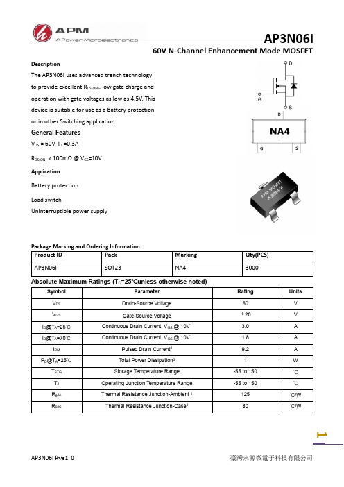
1DescriptionThe AP3N06I uses advanced trench technologyto provide excellent R DS(ON), low gate charge and operation with gate voltages as low as 4.5V. This device is suitable for use as a Battery protection or in other Switching application.General FeaturesV DS = 60V I D =0.3A R DS(ON) < 100m Ω @ V GS =10VApplicationBattery protection Load switchUninterruptible power supplyAbsolute Maximum Ratings (T =25℃unless otherwise noted),=15V , VNote :1.The data tested by surface mounted on a 1 inch2 FR-4 board with 2OZ copper.2.The data tested by pulsed , pulse width ≦300us , duty cycle ≦2%3.The power dissipation is limited by 150℃junction temperature.4.The data is theoretically the same as I D and I DM , in real applications , should be limited by total power dissipation.23150Typical CharacteristicsFig.1 Typical Output Characteristics Fig.2 On-Resistance v.s Gate-SourceFig.3 Forward Characteristics of Reverse Fig.4 Gate-Charge CharacteristicsFig.5 Normalized V v.s TFig.8 Safe Operating AreaFig.9 Normalized Maximum Transient Thermal ImpedanceFig.7 CapacitanceFig.10 Switching Time Waveform Fig.11 Gate Charge Waveform4Package Mechanical Data-SOT235Attention1,Any and all APM Microelectronics products described or contained herein do not have specificationsthat can handle applications that require extremely high levels of reliability, such as life support systems, aircraft's control systems, or other applications whose failure can be reasonably expected to result inserious physical and/or material damage. Consult with your APM Microelectronics representative nearestyou before using any APM Microelectronics products described or contained herein in such applications.2,APM Microelectronics assumes no responsibility for equipment failures that result from using productsat values that exceed, even momentarily, rated values (such as maximum ratings, operating condition ranges, or other parameters) listed in products specifications of any and all APM Microelectronicsproducts described or contained herein.3, Specifications of any and all APM Microelectronics products described or contained here instipulate the performance, characteristics, and functions of the describ ed products in the independent state, and arenot guarantees of the performance, characteristics, and functions of the described products as mountedin the customer’s products or equipment. To verify symptoms and states that cannot be evaluated in an independent device, the customer should always evaluate and test devices mounted in the customer’s products or equipment.4, APM Microelectronics Semiconductor CO., LTD. strives to supply high quality high reliability products. However, any and all semiconductor products fail with some probability. It is possible that theseprobabilistic failures could give rise to accidents or events that could endanger human lives that couldgive rise to smoke or fire, or that could cause damage to other property. When designing equipment,adopt safety measures so that these kinds of accidents or events cannot occur. Such measures includebut are not limited to protective circuits and error prevention circuits for safe design, redundantdesign,and structural design.5,In the event that any or all APM Microelectronics products(including technical data, services) describedor contained herein are controlled under any of applicable local export control laws and regulations, such products must not be exported without obtaining the export license from the authorities concerned in accordance with the above law.6, No part of this publication may be reproduced or transmitted in any form or by any means,electronic or mechanical, including photocopying and recording, or any information storage or retrieval system, or otherwise, without the prior written permission of APM Microelectronics Semiconductor CO., LTD.7, Information (including circuit diagrams and circuit parameters) herein is for example only; it is not guaranteed for volume production. APM Microelectronics believes information herein is accurate andreliable, but no guarantees are made or implied regarding its use or any infringements of intellectualproperty rights or other rights of third parties.8, Any and all information described or contained herein are subject to change without notice due toproduct/technology improvement,etc. When designing equipment, refer to the "Delivery Specification" forthe APM Microelectronics product that you Intend to use.67。
呼吸机专用mos管APG60N10D 60A 100V TO-252

General DescriptionAPG60N10D use advanced SGT MOSFET technology toprovide low RDS(ON), low gate charge, fast switchingand excellent avalanche characteristics.This device is specially designed to get better ruggednessand suitable to use inFeaturesLow RDS(on) & FOMExtremely low switching lossExcellent stability and uniformity or InvertorsApplicationsConsumer electronic power supplyMotor controlSynchronous-rectificationIsolated DCSynchronous-rectification applicationsProduct ID Pack Marking Qty(PCS)APG60N10D TO-252-3APG60N10D XXX YYYY2500at T j=25℃ unless otherwise notedParameter Symbol Value UnitDrain source voltage V DS100 VGate source voltage V GS±20 V Continuous drain current1), T C=25 ℃I D60 APulsed drain current2), T C=25 ℃I D, pulse180 APower dissipation3), T C=25 ℃P D125 WSingle pulsed avalanche energy5)E AS100 mJ Operation and storage temperature T stg,T j-55 to 150 ℃ Thermal resistance, junction-case RθJC 1 ℃/WThermal resistance, junction-ambient4)RθJA62 ℃/W1Electrical Characteristics at T j=25 ℃ unless otherwise specified1)Calculated continuous current based on maximum allowable junction temperature.2)Repetitive rating; pulse width limited by max. junction temperature.3)Pd is based on max. junction temperature, using junction-case thermal resistance.4)The value of RθJA is measured with the device mounted on 1 in 2 FR-4 board with 2oz. Copper, in a stillair environment with T a=25 ℃.5)V DD=50 V, R G=25 Ω, L=0.3 mH, starting T j=25 ℃.23Electrical Characteristics DiagramsV , Drain-source voltage (V) DSFigure 1, Typ. output characteristicsFigure 2, Typ. transfer characteristicsDS45 Test circuits and waveformsFigure 4, Diode reverse recovery test circuit & waveformsFigure 1 , G ate c h arge t e st c i rcuit & w a veformFigure , 2 S w itching t ime t e st c i rcuit & w a veformsFigure , 3 Unclamped i n ductive s w itching (UIS) t e st c i rcuit & w a veforms6Package Mechanical DataDimensionsMillimeters Inches Ref.Min.Typ.Max.Min.Typ.Max.A A2B C DE G H LV1V22.1000.660.40 2.500.100.860.600.08300.0260.0160.0980.0040.0340.0246.409.5010.700.3740.4210.0530.0655.906.30L20°6°0.2320.2486.800.2520.2684.47 4.670.1760.1841.09 1.210.0430.0487°1.351.650°6°7°B2 5.18 5.480.2020.216C20.440.580.0170.023D1E15.30REF4.630.1820.209REFDETAIL ATO-252Reel Spectification-TO-252ABBDimensionsMillimeters Inches Ref.Min.Typ.Max.Min.Typ.Max.W E F D0D1P0P1P2A0B0K0T t115.901.657.401.4016.101.857.601.600.6260.0650.2910.0550.6340.0730.2990.0631.40 1.607.9010.4510.600.4110.4170.240.270.0090.0110.0550.0633.90 4.106.900.27110P00.1540.1618.100.3110.3191.90 2.100.0750.0830.100.00440.001.5752.780.10916.001.757.501.501.504.008.002.0010.500.6300.0690.2950.0590.0590.1570.3150.0790.4136.857.002.68 2.880.2700.2760.1050.11339.8040.201.5671.583APG60N10D100V N-SGT Enhancement Mode MOSFETAttention1,Any and all APM Microelectronics products described or contained herein do not have specificationsthat can handle applications that require extremely high levels of reliability, such as life support systems, aircraft's control systems, or other applications whose failure can be reasonably expected to result inserious physical and/or material damage. Consult with your APM Microelectronics representative nearestyou before using any APM Microelectronics products described or contained herein in such applications.2,APM Microelectronics assumes no responsibility for equipment failures that result from using productsat values that exceed, even momentarily, rated values (such as maximum ratings, operating condition ranges, or other parameters) listed in products specifications of any and all APM Microelectronicsproducts described or contained herein.3, Specifications of any and all APM Microelectronics products described or contained here instipulate the performance, characteristics, and functions of the describ ed products in the independent state, and arenot guarantees of the performance, characteristics, and functions of the described products as mountedin the customer’s products or equipment. To verify symptoms and states that cannot be evaluated in an independent device, the customer should always evaluate and test devices mounted in the customer’s products or equipment.4, APM Microelectronics Semiconductor CO., LTD. strives to supply high quality high reliability products. However, any and all semiconductor products fail with some probability. It is possible that theseprobabilistic failures could give rise to accidents or events that could endanger human lives that couldgive rise to smoke or fire, or that could cause damage to other property. When designing equipment,adopt safety measures so that these kinds of accidents or events cannot occur. Such measures includebut are not limited to protective circuits and error prevention circuits for safe design, redundantdesign,and structural design.5,In the event that any or all APM Microelectronics products(including technical data, services) describedor contained herein are controlled under any of applicable local export control laws and regulations, such products must not be exported without obtaining the export license from the authorities concerned in accordance with the above law.6, No part of this publication may be reproduced or transmitted in any form or by any means,electronic or mechanical, including photocopying and recording, or any information storage or retrieval system, or otherwise, without the prior written permission of APM Microelectronics Semiconductor CO., LTD.7, Information (including circuit diagrams and circuit parameters) herein is for example only; it is not guaranteed for volume production. APM Microelectronics believes information herein is accurate and reliable, but no guarantees are made or implied regarding its use or any infringements of intellectualproperty rights or other rights of third parties.8, Any and all information described or contained herein are subject to change without notice due toproduct/technology improvement,etc. When designing equipment, refer to the "Delivery Specification" forthe APM Microelectronics product that you Intend to use.7。
呼吸机专用mos管APG12N10D 12A 100V TO-252.

1General DescriptionAPG12N10D use advanced SGT MOSFET technology to provide low RDS(ON), low gate charge, fast switching and excellent avalanche characteristics.This device is specially designed to get better ruggednessand suitable to use inFeaturesLow RDS(on) & FOMExtremely low switching lossExcellent stability and uniformity or InvertorsApplicationsConsumer electronic power supply Motor controlSynchronous-rectification Isolated DCSynchronous-rectification applicationsat T j =25℃ unless otherwise notedElectrical Characteristics at T j=25 ℃ unless otherwise specified23Electrical Characteristics DiagramsV DS , Drain-source voltage (V)Figure 3, Typ. capacitancesFigure 4, Typ. gate chargeFigure 5, Drain-source breakdown voltageFigure 6, Drain-source on-state resistanceRD S (O N ) , O n -r e s i s t a n c e ( m Ω )Figure 1, Typ. output characteristics I D , D r a i n c u r r e n t (A )V DS , Drain-source voltage (V)I D , D r a i n c u r r e n t (A )4Figure 9, Drain currentFigure 10, Safe operation area T C =25 ℃Figure 7, Forward characteristic of body diode Figure 8, Drain-source on-state resistanceI S , S o u r c e c u r r e n t (A )V SD , Source-Drain voltage (V)I D , Drain current(A)R D S (O N ), O n -r e s i s t a n c e (Ω)I ASV GSBV DSSV DDEAS=12L x I AS 2 x BV DSS BV DSS -V DDFig.11 Switching Time WaveformFig.12 Unclamped Inductive Switching Waveform5Package Mechanical Data-TO-252-3LDimensionsMillimeters Inches Ref.Min.Typ.Max.Min.Typ.Max.A A2B C DE G H LV1V22.1000.660.40 2.500.100.860.600.08300.0260.0160.0980.0040.0340.0246.409.5010.700.3740.4210.0530.0655.906.30L20°6°0.2320.2486.800.2520.2684.47 4.670.1760.1841.09 1.210.0430.0487°1.351.650°6°7°B2 5.18 5.480.2020.216C20.440.580.0170.023D1E15.30REF4.630.1820.209REFDETAIL ATO-252Reel Spectification-TO-252ABBDimensionsMillimeters Inches Ref.Min.Typ.Max.Min.Typ.Max.W E F D0D1P0P1P2A0B0K0T t115.901.657.401.4016.101.857.601.600.6260.0650.2910.0550.6340.0730.2990.0631.40 1.607.9010.4510.600.4110.4170.240.270.0090.0110.0550.0633.90 4.106.900.27110P00.1540.1618.100.3110.3191.90 2.100.0750.0830.100.00440.001.5752.780.10916.001.757.501.501.504.008.002.0010.500.6300.0690.2950.0590.0590.1570.3150.0790.4136.857.002.68 2.880.2700.2760.1050.11339.8040.201.5671.583Attention1,Any and all APM Microelectronics products described or contained herein do not have specificationsthat can handle applications that require extremely high levels of reliability, such as life support systems, aircraft's control systems, or other applications whose failure can be reasonably expected to result inserious physical and/or material damage. Consult with your APM Microelectronics representative nearestyou before using any APM Microelectronics products described or contained herein in such applications.2,APM Microelectronics assumes no responsibility for equipment failures that result from using productsat values that exceed, even momentarily, rated values (such as maximum ratings, operating conditionranges, or other parameters) listed in products specifications of any and all APM Microelectronicsproducts described or contained herein.3, Specifications of any and all APM Microelectronics products described or contained here instipulate the performance, characteristics, and functions of the describ ed products in the independent state, and arenot guarantees of the performance, characteristics, and functions of the described products as mountedin the customer’s products or equipment. To verify symptoms and states that cannot be evaluated in an independent device, the customer should always evaluate and test devices mounted in the customer’s products or equipment.4, APM Microelectronics Semiconductor CO., LTD. strives to supply high quality high reliability products. However, any and all semiconductor products fail with some probability. It is possible that theseprobabilistic failures could give rise to accidents or events that could endanger human lives that couldgive rise to smoke or fire, or that could cause damage to other property. When designing equipment,adopt safety measures so that these kinds of accidents or events cannot occur. Such measures includebut are not limited to protective circuits and error prevention circuits for safe design, redundantdesign,and structural design.5,In the event that any or all APM Microelectronics products(including technical data, services) describedor contained herein are controlled under any of applicable local export control laws and regulations, such products must not be exported without obtaining the export license from the authorities concerned in accordance with the above law.6, No part of this publication may be reproduced or transmitted in any form or by any means,electronic or mechanical, including photocopying and recording, or any information storage or retrieval system, or otherwise, without the prior written permission of APM Microelectronics Semiconductor CO., LTD.7, Information (including circuit diagrams and circuit parameters) herein is for example only; it is not guaranteed for volume production. APM Microelectronics believes information herein is accurate andreliable, but no guarantees are made or implied regarding its use or any infringements of intellectualproperty rights or other rights of third parties.8, Any and all information described or contained herein are subject to change without notice due toproduct/technology improvement,etc. When designing equipment, refer to the "Delivery Specification" forthe APM Microelectronics product that you Intend to use.6Copyright Attribution“APM-Microelectronice”7。
呼吸机专用mos管APG130N06PT 130A 60V TO-220 TO-23
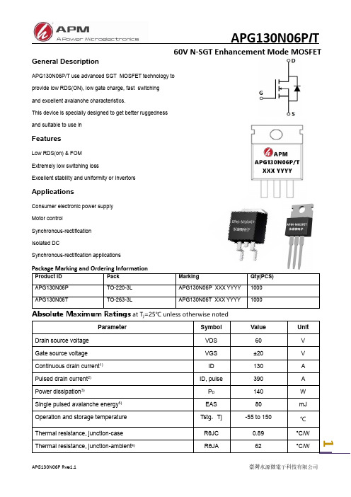
1General DescriptionAPG130N06P/T use advanced SGT MOSFET technology to provide low RDS(ON), low gate charge, fast switching and excellent avalanche characteristics.This device is specially designed to get better ruggednessand suitable to use inFeaturesLow RDS(on) & FOMExtremely low switching lossExcellent stability and uniformity or InvertorsApplicationsConsumer electronic power supply Motor controlSynchronous-rectification Isolated DCSynchronous-rectification applicationsProduct ID Pack MarkingQty(PCS) APG130N06P TO-220-3L APG130N06P XXX YYYY 1000 APG130N06TTO-263-3LAPG130N06T XXX YYYY1000at T j =25℃ unless otherwise notedParameterSymbol Value Unit Drain source voltage VDS 60 V Gate source voltage VGS ±20 V Continuous drain current 1) ID 130 A Pulsed drain current 2) ID, pulse 390 A Power dissipation 3)P D 140 W Single pulsed avalanche energy 5) EAS 80 mJ Operation and storage temperature Tstg ,Tj -55 to 150 ℃ Thermal resistance, junction-case RθJC 0.89 °C/WThermal resistance, junction-ambient 4)RθJA62°C/W2Electrical Characteristics at T j =25 ℃ unless otherwise specifiedParameterSymbol Min. Typ. Max. Unit Test condition Drain-source breakdown voltage BV DSS 60 V V GS =0 V, I D =250 μA Gate threshold voltage V GS(th) 1.0 2.5 V V DS =V GS , I D =250 μA Drain-source on-state resistance R DS(ON) 3.0 3.5 mΩ V GS =10 V, I D =20 A Drain-source on-state resistance R DS(ON) 3.5 4.5 mΩV GS =4.5 V, I D =10 A Gate-source leakage current I GSS100 nA V GS =20 V-100 V GS =-20 V Drain-source leakage current I DSS 1 μA V DS =60 V, V GS =0 VInput capacitance C iss 5377 pF V GS =0 V, V DS =25 V, ƒ=100 kHz Output capacitance C oss 1666 pF Reverse transfer capacitance C rss 77.7 pF Turn-on delay time t d(on) 22.5 ns V GS =10 V, V DS =30 V, R G =2 Ω, I D =25 ARise time t r 6.7 ns Turn-off delay time t d(off) 80.3 ns Fall time t f 26.8 ns Total gate charge Q g 66.1 nC I D =25 A, V DS =30 V, V GS =10 V Gate-source charge Q gs 10.7 nC Gate-drain charge Q gd 10.9 nC Gate plateau voltage V plateau 2.9 VDiode forward current I S 130 A V GS <V th Pulsed source current I SP 390 Diode forward voltage V SD 1.3 V I S =20 A, V GS =0 V Reverse recovery time t rr 68.3 ns I S =25 A, di/dt=100 A/μsReverse recovery charge Q rr 73.0 nC Peak reverse recovery currentI rrm1.9AElectricalCharacteristicsDiagrams34Test circuits and waveformsFigure 1,G ate c h arge t e st c i rcuit & w a veformFigure , 2S w itching t ime t e st c i rcuit & w a veformsFigure , 3Unclamped i n ductive s w itching (UIS) t e st c i rcuit & w a veformsFigure 4, Diode reverse recovery test circuit & waveforms56Attention1,Any and all APM Microelectronics products described or contained herein do not have specificationsthat can handle applications that require extremely high levels of reliability, such as life support systems, aircraft's control systems, or other applications whose failure can be reasonably expected to result inserious physical and/or material damage. Consult with your APM Microelectronics representative nearestyou before using any APM Microelectronics products described or contained herein in such applications.2,APM Microelectronics assumes no responsibility for equipment failures that result from using productsat values that exceed, even momentarily, rated values (such as maximum ratings, operating condition ranges, or other parameters) listed in products specifications of any and all APM Microelectronicsproducts described or contained herein.3, Specifications of any and all APM Microelectronics products described or contained here instipulate the performance, characteristics, and functions of the describ ed products in the independent state, and arenot guarantees of the performance, characteristics, and functions of the described products as mountedin the customer’s products or equipment. To verify symptoms and states that cannot be evaluated in an independent device, the customer should always evaluate and test devices mounted in the customer’s products or equipment.4, APM Microelectronics Semiconductor CO., LTD. strives to supply high quality high reliability products. However, any and all semiconductor products fail with some probability. It is possible that theseprobabilistic failures could give rise to accidents or events that could endanger human lives that couldgive rise to smoke or fire, or that could cause damage to other property. When designing equipment,adopt safety measures so that these kinds of accidents or events cannot occur. Such measures includebut are not limited to protective circuits and error prevention circuits for safe design, redundantdesign,and structural design.5,In the event that any or all APM Microelectronics products(including technical data, services) describedor contained herein are controlled under any of applicable local export control laws and regulations, such products must not be exported without obtaining the export license from the authorities concerned in accordance with the above law.6, No part of this publication may be reproduced or transmitted in any form or by any means,electronic or mechanical, including photocopying and recording, or any information storage or retrieval system, or otherwise, without the prior written permission of APM Microelectronics Semiconductor CO., LTD.7, Information (including circuit diagrams and circuit parameters) herein is for example only; it is not guaranteed for volume production. APM Microelectronics believes information herein is accurate andreliable, but no guarantees are made or implied regarding its use or any infringements of intellectualproperty rights or other rights of third parties.8, Any and all information described or contained herein are subject to change without notice due toproduct/technology improvement,etc. When designing equipment, refer to the "Delivery Specification" forthe APM Microelectronics product that you Intend to use.7。
呼吸机专用mos管 AP5N50D 5A 500V TO-252

Gate-Source Voltage
Single Pulse Avalanche Energy
Avalanche Current
Repetitive Avalanche Energy
Power Dissipation (TC = 25ºC)
Operating Junction and Storage Temperature Range
ID, Drain Current (A)
3
AP5N50D Rve1.0
臺灣永源微電子科技有限公司
AP5N50D
500V N-Channel Enhancement Mode MOSFE
103
10
Ciss
8
VDD = 400V
VDD = 250V
102
C oss
6
VDD = 100V
101
Crss
V(BR)DSS IDSS IGSS VGS(th)
Drain-Source Breakdown Voltage Zero Gate Voltage Drain Current Gate-Source Leakage Gate-Source Threshold Voltage
VGS = 0V, ID = 250µA
-- 13.5 --
Qgs
Gate-Source Charge
Qgd
Gate-Drain Charge
VDD = 400V, ID = 5A, VGS = 10V
--
2
--
nC
--
6
--
td(on)
Turn-on Delay Time
tr
Turn-on Rise Time
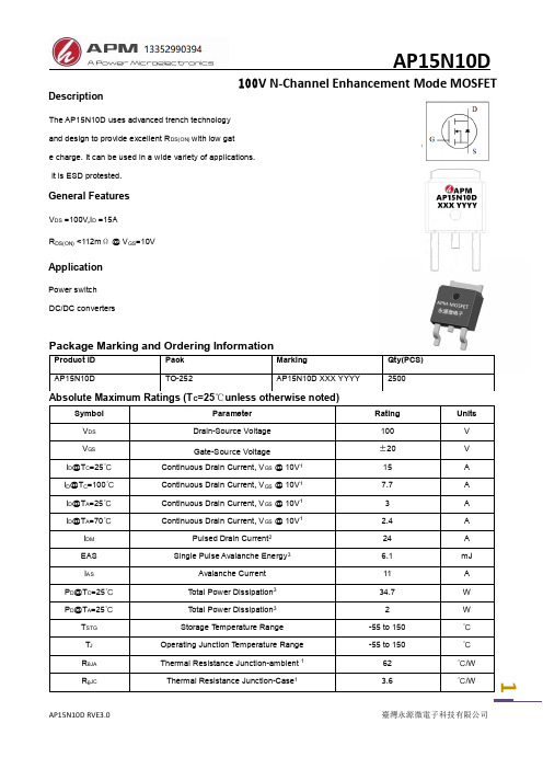
筋膜枪专用mos管AP15N10D_15A_100V_TO-252
TSTG
Storage Temperature Range
-55 to 150
TJ
Operating Junction Temperature Range
-55 to 150
RθJA
Thermal Resistance Junction-ambient 1
62
RθJC
Thermal Resistance Junction-Case1
Marking
Qty(PCS)
AP15N10D
TO-252
AP15N10D XXX YYYY
2500
Absolute Maximum Ratings (TC=25℃unless otherwise noted)
Symbol
Parameter
Rating
VDS VGS ID@TC=25℃ ID@TC=100℃ ID@TA=25℃ ID@TA=70℃ IDM
Description
AP15N10D
100V N-Channel Enhancement Mode MOSFET
The AP15N10D uses advanced trench technology and design to provide excellent RDS(ON) with low gat e charge. It can be used in a wide variety of applications. It is ESD protested.
2
AP15N10D RVE3.0
臺灣永源微電子科技有限公司
Typical Characteristics
25 20 15 10
AP15N10D
呼吸机专用mos管 AP30P03D -30A -30V TO-252

AP30P03D RVE3.0 臺灣永源微電子科技有限公司1DescriptionThe AP30P03D uses advanced trench technologyto provide excellent R DS(ON), low gate charge andoperation with gate voltages as low as 4.5V. Thisdevice is suitable for use as aBattery protection or in other Switching application.General FeaturesV DS = -30V I D =-30 AR DS(ON) < 20mΩ @ V GS=10VApplicationBattery protectionLoad switchUninterruptible power supplyPackage Marking and Ordering InformationProduct ID Pack Marking Qty(PCS) AP30P03D TO-252-3AP30P03D XXXX YYYY2500 Absolute Maximum Ratings (T C=25℃unless otherwise noted)Symbol ParameterRatingUnits 10s Steady StateV DS Drain-Source Voltage-30 V V GS Gate-Sou r ce Voltage ±20VI D@T C=25℃Continuous Drain Current, V GS @ -10V1-30 A I D@T C=100℃Continuous Drain Current, V GS @ -10V1-22 A I D@T A=25℃Continuous Drain Current, V GS @ -10V1-13.4 -8.5 A I D@T A=70℃Continuous Drain Current, V GS @ -10V1-10.7 -6.8 AI DM Pulsed Drain Current2-70 AEAS Single Pulse Avalanche Energy372.2 mJI AS Avalanche Current -38 A P D@T C=25℃Total Power Dissipation434.7 W P D@T A=25℃Total Power Dissipation4 5 2 W T STG Storage Temperature Range -55 to 150 ℃ T J Operating Junction Temperature Range -55 to 150 ℃ RθJA Thermal Resistance Junction-Ambient 162 ℃/W RθJA Thermal Resistance Junction-Ambient 1 (t ≤10s) 25 ℃/W RθJC Thermal Resistance Junction-Case1 3.6 ℃/WAP30P03D RVE3.0 臺灣永源微電子科技有限公司2J Symbol Parameter Conditions Min. Typ. Max. Unit BV DSS Drain-Source Breakdown Voltage V GS =0V , I D =-250uA -30 --- --- V △BV DSS /△T J BV DSS Temperature Coefficient Reference to 25℃ , I D =-1mA--- -0.022 --- V/℃R DS(ON) Static Drain-Source On-Resistance 2 V GS =-10V , I D =-15A--- 18 20 m Ω V GS =-4.5V , I D =-10A --- 25 32 V GS(th) Gate Threshold VoltageV GS =V DS , I D =-250uA-1.0 --- -2.5 V △V GS(th) V GS(th) Temperature Coefficient --- 4.6 --- mV/℃ I DSS Drain-Source Leakage Current V DS =-24V , V GS =0V , T J =25℃--- --- -1 uA V DS =-24V , V GS =0V , T J =55℃ --- --- -5 I GSS Gate-Source Leakage Current V GS =±20V , V DS =0V --- --- ±100 nA gfs Forward Transconductance V DS =-5V , I D =-10A --- 5 --- S R g Gate Resistance V DS =0V , V GS =0V , f=1MHz--- 13 --- Ω Q g Total Gate Charge (-4.5V) V DS =-15V , V GS =-4.5V , I D =-15A ---12.5 --- nC Q gs Gate-Source Charge ---5.4 --- Q gd Gate-Drain Charge --- 5 --- T d(on) Turn-On Delay Time V DD =-15V , V GS =-10V,R G =3.3, I D =-15A--- 4.4 --- ns T r Rise Time --- 11.2 --- T d(off) Turn-Off Delay Time --- 34 --- T f Fall Time --- 18 --- C iss Input Capacitance V DS =-15V , V GS =0V , f=1MHz --- 1345 --- pF C oss Output Capacitance --- 194 --- C rss Reverse Transfer Capacitance --- 158 --- I S Continuous Source Current 1,5 V G =V D =0V , Force Current --- --- -35 A I SM Pulsed Source Current 2,5 --- --- -70 A V SD Diode Forward Voltage 2 V GS =0V , I S =-1A , T J =25℃ --- --- -1.2 V t rr Reverse Recovery Time I F =-15A , dI/dt=100A/µs , T J =25℃--- 12.4 --- nS Q rrReverse Recovery Charge---5---nC-30V P-Channel Enhancement Mode MOSFET3150 Fig.1 Typical Output CharacteristicsFig.2 On-Resistance v.s Gate-Source Fig.3 Forward Characteristics of Reverse Fig.4 Gate-Charge Characteristics Fig.5 Normalized V GS(th) v.s T J4Fig.8 Safe Operating Area Fig.9 Normalized Maximum Transient Thermal Impedance Fig.7 Capacitance Fig.10 Switching Time Waveform Fig.11 Unclamped Inductive Switching WaveformAP30P03D RVE3.0 臺灣永源微電子科技有限公司5Package Mechanical DataDimensionsMillimeters Inches Ref.Min.Typ.Max.Min.Typ.Max.A A2B C DE G H LV1V22.1000.660.40 2.500.100.860.600.08300.0260.0160.0980.0040.0340.0246.409.5010.700.3740.4210.0530.0655.906.30L20°6°0.2320.2486.800.2520.2684.47 4.670.1760.1841.09 1.210.0430.0487°1.351.650°6°7°B2 5.18 5.480.2020.216C20.440.580.0170.023D1E15.30REF4.630.1820.209REFB2E HBGLC2DETAIL ADETAIL AACV 1V 1V 2A 2DV 1E1D 1L2TO-252Reel Spectification-TO-252WEFD 0P0P2P1D 1Tt1B 0K0A05°AAA BBB BDimensionsMillimeters Inches Ref.Min.Typ.Max.Min.Typ.Max.W E F D0D1P0P1P2A0B0K0T t115.901.657.401.4016.101.857.601.600.6260.0650.2910.0550.6340.0730.2990.0631.40 1.607.9010.4510.600.4110.4170.240.270.0090.0110.0550.0633.90 4.106.900.27110P00.1540.1618.100.3110.3191.90 2.100.0750.0830.100.00440.001.5752.780.109Φ329Φ132016.001.757.501.501.504.008.002.0010.500.6300.0690.2950.0590.0590.1570.3150.0790.4136.857.002.68 2.880.2700.2760.1050.11339.8040.201.5671.583Attention1,Any and all APM Microelectronics products described or contained herein do not have specificationsthat can handle applications that require extremely high levels of reliability, such as life support systems, aircraft's control systems, or other applications whose failure can be reasonably expected to result inserious physical and/or material damage. Consult with your APM Microelectronics representative nearestyou before using any APM Microelectronics products described or contained herein in such applications.2,APM Microelectronics assumes no responsibility for equipment failures that result from using productsat values that exceed, even momentarily, rated values (such as maximum ratings, operating condition ranges, or other parameters) listed in products specifications of any and all APM Microelectronicsproducts described or contained herein.3, Specifications of any and all APM Microelectronics products described or contained here instipulate the performance, characteristics, and functions of the describ ed products in the independent state, and arenot guarantees of the performance, characteristics, and functions of the described products as mountedin the customer’s products or equipment. To verify symptoms and states that cannot be evaluated in an independent device, the customer should always evaluate and test devices mounted in the customer’s products or equipment.4, APM Microelectronics Semiconductor CO., LTD. strives to supply high quality high reliability products. However, any and all semiconductor products fail with some probability. It is possible that theseprobabilistic failures could give rise to accidents or events that could endanger human lives that couldgive rise to smoke or fire, or that could cause damage to other property. When designing equipment,adopt safety measures so that these kinds of accidents or events cannot occur. Such measures includebut are not limited to protective circuits and error prevention circuits for safe design, redundantdesign,and structural design.5,In the event that any or all APM Microelectronics products(including technical data, services) describedor contained herein are controlled under any of applicable local export control laws and regulations, such products must not be exported without obtaining the export license from the authorities concerned in accordance with the above law.6, No part of this publication may be reproduced or transmitted in any form or by any means,electronic or mechanical, including photocopying and recording, or any information storage or retrieval system, or otherwise, without the prior written permission of APM Microelectronics Semiconductor CO., LTD.7, Information (including circuit diagrams and circuit parameters) herein is for example only; it is not guaranteed for volume production. APM Microelectronics believes information herein is accurate andreliable, but no guarantees are made or implied regarding its use or any infringements of intellectualproperty rights or other rights of third parties.8, Any and all information described or contained herein are subject to change without notice due toproduct/technology improvement,etc. When designing equipment, refer to the "Delivery Specification" forthe APM Microelectronics product that you Intend to use.6AP30P03D RVE3.0 臺灣永源微電子科技有限公司。
呼吸机专用mos管APG20N10D 20A 100V TO-252

1General DescriptionAPG20N10D use advanced SGT MOSFET technology to provide low RDS(ON), low gate charge, fast switching and excellent avalanche characteristics.This device is specially designed to get better ruggednessand suitable to use inFeaturesLow RDS(on) & FOMExtremely low switching lossExcellent stability and uniformity or InvertorsApplicationsConsumer electronic power supply Motor controlSynchronous-rectification Isolated DCSynchronous-rectification applicationsat T j =25℃ unless otherwise notedElectrical Characteristics at T j=25 ℃ unless otherwise specifiedNote1)Calculated continuous current based on maximum allowable junction temperature.2)Repetitive rating; pulse width limited by max. junction temperature.3)Pd is based on max. junction temperature, using junction-case thermal resistance.4)V DD=50 V, R G=50 Ω, L=0.3 mH, starting T j=25 °C.5)The value of RθJA is measured with the device mounted on 1 in 2 FR-4 board with 2oz. Copper, in a stillair environment with T a=25 °C.2Electrical Characteristics DiagramsV DS, Drain-source voltage (V)Figure 5, Drain-source breakdown voltage Figure 6, Drain-source on-state resistance34 APG20N10D R ev1.0APG20N10D R ev 1.0 臺灣永源微電子科技有限公司5Figure 4, Diode reverse recovery test circuit & waveformsFigure 1 , G ate c h arge t e st c i rcuit & w a veformFigure , 2 S w itching t ime t e st c i rcuit & w a veformsFigure , 3 Unclamped i n ductive s w itching (UIS) t e st c i rcuit & w a veformsAPG20N10D R ev 1.0 6Package Mechanical DataDimensionsMillimeters Inches Ref.Min.Typ.Max.Min.Typ.Max.A A2B C DE G H LV1V22.1000.660.40 2.500.100.860.600.08300.0260.0160.0980.0040.0340.0246.409.5010.700.3740.4210.0530.0655.906.30L20°6°0.2320.2486.800.2520.2684.47 4.670.1760.1841.09 1.210.0430.0487°1.351.650°6°7°B2 5.18 5.480.2020.216C20.440.580.0170.023D1E15.30REF4.630.1820.209REFDETAIL ATO-252Reel Spectification-TO-252ABBDimensionsMillimeters Inches Ref.Min.Typ.Max.Min.Typ.Max.W E F D0D1P0P1P2A0B0K0T t115.901.657.401.4016.101.857.601.600.6260.0650.2910.0550.6340.0730.2990.0631.40 1.607.9010.4510.600.4110.4170.240.270.0090.0110.0550.0633.90 4.106.900.27110P00.1540.1618.100.3110.3191.90 2.100.0750.0830.100.00440.001.5752.780.10916.001.757.501.501.504.008.002.0010.500.6300.0690.2950.0590.0590.1570.3150.0790.4136.857.002.68 2.880.2700.2760.1050.11339.8040.201.5671.583Attention1,Any and all APM Microelectronics products described or contained herein do not havespecifications that can handle applications that require extremely high levels of reliability, such aslife support systems, aircraft's control systems, or other applications whose failure can bereasonably expected to result in serious physical and/or material damage. Consult with your APM Microelectronics representative nearest you before using any APM Microelectronics productsdescribed or contained herein in such applications.2,APM Microelectronics assumes no responsibility for equipment failures that result from usingproducts at values that exceed, even momentarily, rated values (such as maximum ratings,operating condition ranges, or other parameters) listed in products specifications of any and all APM Microelectronics products described or contained herein.3, Specifications of any and all APM Microelectronics products described or contained hereinstipulate the performance, characteristics, and functions of the described products in theindependent state, and are not guarantees of the performance, characteristics, and functions of the described products as mounted in the customer’s products or equipment. To verify symptoms andstates that cannot be evaluated in an independent device, the customer should always evaluate andtest devices mounted in the customer’s products or equipment.4, APM Microelectronics Semiconductor CO., LTD. strives to supply high quality high reliability products. However, any and all semiconductor products fail with some probability. It is possible thatthese probabilistic failures could give rise to accidents or events that could endanger human livesthat could give rise to smoke or fire, or that could cause damage to other property. When designing equipment, adopt safety measures so that these kinds of accidents or events cannot occur. Such measures include but are not limited to protective circuits and error prevention circuits for safedesign, redundant design,and structural design.5,In the event that any or all APM Microelectronics products(including technical data, services) described or contained herein are controlled under any of applicable local export control laws and regulations, such products must not be exported without obtaining the export license from theauthorities concerned in accordance with the above law.6, No part of this publication may be reproduced or transmitted in any form or by anymeans,electronic or mechanical, including photocopying and recording, or any information st orageor retrieval system, or otherwise, without the prior written permission of APM Microelectronics Semiconductor CO., LTD.7, Information (including circuit diagrams and circuit parameters) herein is for example only; it is not guaranteed for volume production. APM Microelectronics believes information herein is accurateand reliable, but no guarantees are made or implied regarding its use or any infringements ofintellectual property rights or other rights of third parties.8, Any and all information described or contained herein are subject to change without notice due to product/technology improvement,etc. When designing equipment, refer to the "Delivery Specification" for the APM Microelectronics product that you Intend to use.7 APG20N10D R ev1.0。
呼吸机专用mos管 AP5G06S 5A 60V SOP-8

60V N+P-Channel Enhancement Mode MOSFET
N-Channel Typical Characteristics
12
10
VGS=10V
VGS=7
8
VGS=5V
35
ID=12A
33
VGS=4.5V
6
VGS=3V
30
RDSON (mΩ)
ID Drain Current (A)
Description
AP5G06S
60V N+P-Channel Enhancement Mode MOSFET
The AP5G06S uses advanced trench technology to provide excellent RDS(ON), low gate charge and operation with gate voltages as low as 4.5V. This device is suitable for use as a Battery protection or in other Switching application.
IDSS
IGSS gfs Rg Qg Qgs Qgd Td(on) Tr Td(off) Tf Ciss Coss Crss
IS ISM
Drain-Source Leakage Current
Gate-Source Leakage Current Forward Transconductance Gate Resistance Total Gate Charge (-4.5V) Gate-Source Charge Gate-Drain Charge Turn-On Delay Time Rise Time Turn-Off Delay Time Fall Time Input Capacitance Output Capacitance Reverse Transfer Capacitance Continuous Source Current1,5 Pulsed Source Current2,5
呼吸机专用mos管 AP30P04D - 30A -40V TO-252
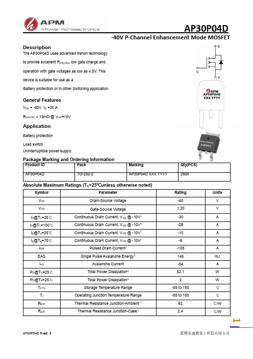
-40V P-Channel Enhancement Mode MOSFET
Description
The AP30P04D uses advanced trench technology
to provide excellent RDS(ON), low gate charge and
S
Rg
Gate Resistance
VDS=0V , VGS=0V , f=1MHz
---
7
14
Qg
Total Gate Charge (-4.5V)
--- 27.9 ---
Qgs
Gate-Source Charge
Qgd
Gate-Drain Charge
VDS=-20V , VGS=-4.5V , ID=-12A ---
ns
ID=-1A
---
9.6
---
Ciss
Input Capacitance
--- 3500 ---
Coss
Output Capacitance
Crss
Reverse Transfer Capacitance
VDS=-15V , VGS=0V , f=1MHz
---
323
---
pF
--- 222 ---
-55 to 150 -55 to 150
62 2.4
Units V V A A A A A mJ A W W ℃ ℃
℃/W ℃/W
1
AP30P04D Rve3.8
臺灣永源微電子科技有限公司
AP30P04D
-40V P-Channel Enhancement Mode MOSFET
呼吸机专用mos管 AP30N10P 30A 100V TO-220
AP30N10P R ve 1.0 臺灣永源微電子科技有限公司1DescriptionThe AP30N10P uses advanced trench technology to provide excellent R DS(ON), low gate charge and operation with gate voltages as low as 4.5V. This device is suitable for use as aBattery protection or in other Switching application.General FeaturesV DS = 100V I D =30 A R DS(ON) < 40mΩ @ V GS =10VApplicationBattery protection Load switchUninterruptible power supplyAbsolute Maximum Ratings (T C =25℃unless otherwise noted)AP30N10P R ve 1.0 臺灣永源微電子科技有限公司2R θJA Thermal Resistance Junction-ambient 1 62 ℃/W R θJCThermal Resistance Junction-Case 11.2℃/WElectrical Characteristics (T J =25℃, unless otherwise noted)Symbol ParameterConditionsMin. Typ. Max. Unit BV DSSDrain-Source Breakdown VoltageV GS =0V , I D =250uA 100 --- --- V △BV DSS /△T J BVDSS Temperature CoefficientReference to 25℃ , I D =1mA --- 0.098 --- V/℃ R DS(ON) Static Drain-Source On-Resistance 2 V GS =10V , I D =16A--- 36 40 m Ω V GS =4.5V , I D =10A --- --- 50 V GS(th) Gate Threshold Voltage V GS =V DS , I D =250uA 1.5 --- 2.5 V △V GS(th)V GS(th) Temperature Coefficient--- -5.52 --- mV/℃I DSS Drain-Source Leakage Current V DS =80V , V GS =0V , T J =25℃--- --- 10 uA V DS =80V , V GS =0V , T J =55℃ --- --- 100 I GSS Gate-Source Leakage Current V GS =±20V , V DS =0V --- --- ±100 nA gfs Forward Transconductance V DS =5V , I D =16A --- 30 --- S R g Gate Resistance V DS =0V , V GS =0V , f=1MHz--- 1.6 --- Q g Total Gate Charge (10V) V DS =80V , V GS =10V , I D =16A--- 45.6 --- nCQ gs Gate-Source Charge --- 6.7 --- Q gd Gate-Drain Charge --- 11.8 --- T d(on) Turn-On Delay Time V DD =50V , V GS =10V , R G =3.3 I D =10A---12 --- nsT r Rise Time --- 32.2 --- T d(off) Turn-Off Delay Time --- 42 --- T f Fall Time --- 13.4 --- C iss Input Capacitance V DS =25V , V GS =0V , f=1MHz --- 2270 --- pF C oss Output Capacitance --- 130 --- C rss Reverse Transfer Capacitance --- 90 --- I S Continuous Source Current 1,5 V G =V D =0V , Force Current --- --- 36 A V SD Diode Forward Voltage 2 V GS =0V , I S =1A , T J =25℃ --- --- 1.2 V t rr Reverse Recovery Time I F =16A , dI/dt=100A/µs , T J =25℃--- 33 --- nS Q rrReverse Recovery Charge---28---nC3Typical CharacteristicsFig.1 Typical Output Characteristics Fig.2 On-Resistance vs. G-S Voltage Fig.3 Source Drain Forward Characteristics Fig.4 Gate-Charge CharacteristicsFig.5 Normalized V GS(th) vs. T JFig.6 Normalized R DSON vs. T J4I ASV GSBV DSSV DDEAS=12L x I AS 2 x BV DSS BV DSS -V DDFig.8 Safe Operating AreaFig.7 CapacitanceFig.10 Switching Time Waveform Fig.11 Unclamped Inductive Switching Waveform56 AP30N10P R ve1.0 臺灣永源微電子科技有限公司Attention1,Any and all APM Microelectronics products described or contained herein do not have specificationsthat can handle applications that require extremely high levels of reliability, such as life support systems, aircraft's control systems, or other applications whose failure can be reasonably expected to result inserious physical and/or material damage. Consult with your APM Microelectronics representative nearestyou before using any APM Microelectronics products described or contained herein in such applications.2,APM Microelectronics assumes no responsibility for equipment failures that result from using productsat values that exceed, even momentarily, rated values (such as maximum ratings, operating conditionranges, or other parameters) listed in products specifications of any and all APM Microelectronicsproducts described or contained herein.3, Specifications of any and all APM Microelectronics products described or contained here instipulate the performance, characteristics, and functions of the describ ed products in the independent state, and arenot guarantees of the performance, characteristics, and functions of the described products as mountedin the customer’s products or equipment. To verify symptoms and states that cannot be evaluated in an independent device, the customer should always evaluate and test devices mounted in the customer’s products or equipment.4, APM Microelectronics Semiconductor CO., LTD. strives to supply high quality high reliability products. However, any and all semiconductor products fail with some probability. It is possible that theseprobabilistic failures could give rise to accidents or events that could endanger human lives that couldgive rise to smoke or fire, or that could cause damage to other property. When designing equipment,adopt safety measures so that these kinds of accidents or events cannot occur. Such measures includebut are not limited to protective circuits and error prevention circuits for safe design, redundantdesign,and structural design.5,In the event that any or all APM Microelectronics products(including technical data, services) describedor contained herein are controlled under any of applicable local export control laws and regulations, such products must not be exported without obtaining the export license from the authorities concerned in accordance with the above law.6, No part of this publication may be reproduced or transmitted in any form or by any means,electronic or mechanical, including photocopying and recording, or any information storage or retrieval system, or otherwise, without the prior written permission of APM Microelectronics Semiconductor CO., LTD.7, Information (including circuit diagrams and circuit parameters) herein is for example only; it is not guaranteed for volume production. APM Microelectronics believes information herein is accurate andreliable, but no guarantees are made or implied regarding its use or any infringements of intellectualproperty rights or other rights of third parties.8, Any and all information described or contained herein are subject to change without notice due toproduct/technology improvement,etc. When designing equipment, refer to the "Delivery Specification" forthe APM Microelectronics product that you Intend to use.7 AP30N10P R ve1.0 臺灣永源微電子科技有限公司。
AP30N06D 30A 60V TO-252
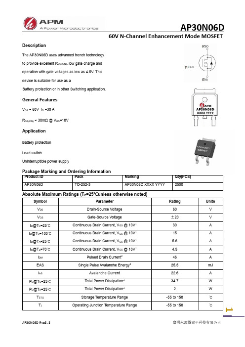
DescriptionThe AP30N06D uses advanced trench technologyto provide excellent R DS(ON), low gate charge andoperation with gate voltages as low as 4.5V. Thisdevice is suitable for use as aBattery protection or in other Switching application.General FeaturesV DS = 60V I D =30 AR DS(ON) < 30mΩ @ V GS=10VApplicationBattery protectionLoad switchUninterruptible power supplyPackage Marking and Ordering InformationProduct ID Pack Marking Qty(PCS)AP30N06D TO-252-3AP30N06D XXXX YYYY2500Absolute Maximum Ratings (T C=25℃unless otherwise noted)Symbol Parameter Rating UnitsV DS Drain-Source Voltage60 VV GS Gate-Sou r ce Voltage ±20VI D@T C=25℃Continuous Drain Current, V GS @ 10V130 AI D@T C=100℃Continuous Drain Current, V GS @ 10V115 AI D@T A=25℃Continuous Drain Current, V GS @ 10V1 5.6 AI D@T A=70℃Continuous Drain Current, V GS @ 10V1 4.5 AI DM Pulsed Drain Current246 AEAS Single Pulse Avalanche Energy325.5 mJI AS Avalanche Current 22.6 AP D@T C=25℃Total Power Dissipation434.7 WP D@T A=25℃Total Power Dissipation4 2 W T STG Storage Temperature Range -55 to 150 ℃T J Operating Junction Temperature Range -55 to 150 ℃1 AP30N06D R ve3.8 臺灣永源微電子科技有限公司AP30N06D R ve 3.8 臺灣永源微電子科技有限公司2R θJA Thermal Resistance Junction-Ambient 1 62 ℃/W R θJCThermal Resistance Junction-Case 13.6℃/WJ Symbol ParameterConditionsMin. Typ. Max. Unit BV DSSDrain-Source Breakdown VoltageV GS =0V , I D =250uA 60 --- --- V △BV DSS /△T J BV DSS Temperature CoefficientReference to 25℃ , I D =1mA --- 0.063 --- V/℃R DS(ON) Static Drain-Source On-Resistance 2V GS =10V , I D =15A--- 25 30 m Ω V GS =4.5V , I D =10A--- 30 38 V GS(th) Gate Threshold Voltage V GS =V DS , I D =250uA 1.2 --- 2.5 V △V GS(th) V GS(th) Temperature Coefficient --- -5.24 --- mV/℃ I DSS Drain-Source Leakage Current V DS =48V , V GS =0V , T J =25℃ --- --- 1 uA V DS =48V , V GS =0V , T J =55℃ --- --- 5 I GSS Gate-Source Leakage Current V GS =±20V , V DS =0V --- --- ±100 nA gfs Forward Transconductance V DS =5V , I D =15A --- 17 --- S R g Gate Resistance V DS =0V , V GS =0V , f=1MHz--- 3.2 --- Ω Q g Total Gate Charge (4.5V) V DS =48V , V GS =4.5V , I D =12A --- 12.6 --- nC Q gs Gate-Source Charge --- 3.2 --- Q gd Gate-Drain Charge --- 6.3 --- T d(on) Turn-On Delay Time V DD =30V , V GS =10V , R G =3.3, I D =10A--- 8 --- ns T r Rise Time --- 14.2 --- T d(off) Turn-Off Delay Time --- 24.4 --- T f Fall Time --- 4.6 --- C iss Input Capacitance V DS =15V , V GS =0V , f=1MHz --- 1378 --- pF C oss Output Capacitance --- 86 --- C rss Reverse Transfer Capacitance --- 64 --- I S Continuous Source Current 1,5 V G =V D =0V , Force Current --- --- 23 A I SM Pulsed Source Current 2,5 --- --- 46 A V SDDiode Forward Voltage 2V GS =0V , I S =1A , T J =25℃ ------1.2V Note :1.The data tested by surface mounted on a 1 inch2 FR-4 board with 2OZ copper.2.The data tested by pulsed , pulse width ≦ 300us , duty cycle ≦ 2%3.The EAS data shows Max. rating . The test condition is VDD=25V,VGS=10V,L=0.1mH,IAS=22.6A4.The power dissipation is limited by 150℃ junction temperature5.The data is theoretically the same as ID and IDM , in real applications , should be limited by total power dissipation.3150Typical Characteristics Fig.1 Typical Output Characteristics Fig.2 On-Resistance v.s Gate-SourceFig.5 Normalized V GS(th) v.s T JFig.3 Forward Characteristics of Reverse Fig.4 Gate-Charge Characteristics4I ASV GSBV DSS V DDEAS=12L x I AS 2 x BV DSSBV DSS -V DDFig.8 Safe Operating Area Fig.7 Capacitance Fig.10 Switching Time Waveform Fig.11 Unclamped Inductive Waveform5Package Mechanical DataDimensionsMillimeters Inches Ref.Min.Typ.Max.Min.Typ.Max.A A2B C D E G H LV1V22.1000.660.40 2.500.100.860.600.08300.0260.0160.0980.0040.0340.0246.409.5010.700.3740.4210.0530.0655.906.30L20°6°0.2320.2486.800.2520.2684.47 4.670.1760.1841.09 1.210.0430.0487°1.35 1.650°6°7°B2 5.18 5.480.2020.216C20.440.580.0170.023D1E15.30REF4.630.1820.209REFDETAIL ATO-252Reel Spectification-TO-252 ABBDimensionsMillimeters Inches Ref.Min.Typ.Max.Min.Typ.Max.W E F D0D1P0P1P2A0B0K0T t115.901.657.401.4016.101.857.601.600.6260.0650.2910.0550.6340.0730.2990.0631.40 1.607.9010.4510.600.4110.4170.240.270.0090.0110.0550.0633.90 4.106.900.27110P00.1540.1618.100.3110.3191.90 2.100.0750.0830.100.00440.001.5752.780.10916.001.757.501.501.504.008.002.0010.500.6300.0690.2950.0590.0590.1570.3150.0790.4136.857.002.68 2.880.2700.2760.1050.11339.8040.201.5671.583Attention1,Any and all APM Microelectronics products described or contained herein do not have specifications that can handle applications that require extremely high levels of reliability, such as life support systems, aircraft's control systems, or other applications whose failure can be reasonably expected to result in serious physical and/or material damage. Consult with your APM Microelectronics representative nearest you before using any APM Microelectronics products described or contained herein in such applications. 2,APM Microelectronics assumes no responsibility for equipment failures that result from using products at values that exceed, even momentarily, rated values (such as maximum ratings, operating condition ranges, or other parameters) listed in products specifications of any and all APM Microelectronics products described or contained herein.3, Specifications of any and all APM Microelectronics products described or contained here instipulate the performance, characteristics, and functions of the described products in the independent state, and are not guarantees of the performance, characteristics, and functions of the described products as mounted in the customer’s products or equipment. To verify symptoms and states that cannot be evaluated in an independent device, the customer should always evaluate and test devices mounted in the customer’s products or equipment.4, APM Microelectronics Semiconductor CO., LTD. strives to supply high quality high reliability products. However, any and all semiconductor products fail with some probability. It is possible that these probabilistic failures could give rise to accidents or events that could endanger human lives that could give rise to smoke or fire, or that could cause damage to other property. When designing equipment, adopt safety measures so that these kinds of accidents or events cannot occur. Such measures include but are not limited to protective circuits and error prevention circuits for safe design, redundantdesign,and structural design.5,In the event that any or all APM Microelectronics products(including technical data, services) described or contained herein are controlled under any of applicable local export control laws and regulations, such products must not be exported without obtaining the export license from the authorities concerned in accordance with the above law.6, No part of this publication may be reproduced or transmitted in any form or by any means,electronic or mechanical, including photocopying and recording, or any information storage or retrieval system, or otherwise, without the prior written permission of APM Microelectronics Semiconductor CO., LTD.7, Information (including circuit diagrams and circuit parameters) herein is for example only; it is not guaranteed for volume production. APM Microelectronics believes information herein is accurate and reliable, but no guarantees are made or implied regarding its use or any infringements of intellectual property rights or other rights of third parties.8, Any and all information described or contained herein are subject to change without notice due to product/technology improvement,etc. When designing equipment, refer to the "Delivery Specification" for the APM Microelectronics product that you Intend to use.6。
呼吸机专用mos管APG130N06D 130A 60V TO-252

Qrr
68.3 73.0
ns IS=25 A, di/dt=100 nC A/μs
Peak reverse recovery current
Irrm
1.9
A
1、Calculated continuous current based on maximum allowable junction temperature.
nC VGS=10 V
V
Diode forward current
IS
130
Pulsed source current
ISP
Diode forward voltage
VSD
390
A
VGS<Vth
1.3
V IS=20 A, VGS=0 V
Reverse recovery time
trr
Reverse recovery charge
VGS ID
ID, pulse PD EAS
Tstg,Tj
±20 130 390 140 80 -55 to 150
Unit V V A A W mJ ℃
Thermal resistance, junction-case Thermal resistance, junction-ambient4)
RθJC RθJA
1.575 1.583
APG60N10D Rve1.0
臺灣永源微電子科技有限公司
APG130N06PIT
60V N-SGT Enhancement Mode MOSFET Attention
1,Any and all APM Microelectronics products described or contained herein do not have specifications that can handle applications that require extremely high levels of reliability, such as life support systems, aircraft's control systems, or other applications whose failure can be reasonably expected to result in serious physical and/or material damage. Consult with your APM Microelectronics representative nearest you before using any APM Microelectronics products described or contained herein in such applications.
呼吸机专用mos管APG40N10D 40A 100V TO-252

General DescriptionAPG40N10D use advanced SGT MOSFET technology toprovide low RDS(ON), low gate charge, fast switchingand excellent avalanche characteristics.This device is specially designed to get better ruggednessand suitable to use inFeaturesLow RDS(on) & FOMExtremely low switching lossExcellent stability and uniformity or InvertorsApplicationsConsumer electronic power supplyMotor controlSynchronous-rectificationIsolated DCSynchronous-rectification applicationsProduct ID Pack Marking Qty(PCS)APG40N10D TO-252-3APG40N10D XXX YYYY2500Absolute Maximum Ratings at T j=25℃ unless otherwise notedParameter Symbol Value UnitDrain source voltage VDS 100 VGate source voltage VGS ±20 V Continuous drain current1), T C=25 ℃ID 40 APulsed drain current2), T C=25 ℃ID, pulse 120 APower dissipation3), T C=25 ℃P D72 WSingle pulsed avalanche energy5)EAS 30 mJOperation and storage temperature Tstg,Tj -55 to 150 ℃1 APG40N10D R ev1.0 臺灣永源微電子科技有限公司APG40N10D R ev 1.0 臺灣永源微電子科技有限公司2ParameterSymbol Value Unit Thermal resistance, junction-case RθJC 1.74 ℃/W Thermal resistance, junction-ambient 4)RθJA62℃/Wat T j =25 ℃ unless otherwise specifiedParameterSymbol Test condition Min. Typ. Max. Unit Drain-source breakdown voltageBV DSS V GS =0 V, I D =250 μA 100 V Gate threshold voltage V GS(th) V DS =V GS , I D =250 μA 1.0 2.5 V Drain-source on-state resistanceR DS(ON) V GS =10 V, I D =8 A 16 20 mΩ Drain-source on-state resistanceR DS(ON) V GS =4.5 V, I D =6 A26 mΩ Gate-source leakage current I GSS100 nA V GS =20 V-100 Drain-source leakage current I DSS V DS =100 V, V GS =0 V1 μA Input capacitance Ciss V GS =0 V, V DS =50 V, ƒ=1 MHz1190.6 pF Output capacitanceCoss 194.6 pF Reverse transfer capacitance Crss 4.1 pF Turn-on delay time td(on) V GS =10 V, V DS =50 V, R G =2.2 Ω, I D =10A17.8 ns Rise timet r 3.9 ns Turn-off delay time td(off) 33.5 ns Fall time t f 3.2 ns Total gate charge Q g I D =8 A, V DS =50 V, V GS =10 V 19.8 nC Gate-source charge Q gs 2.4 nC Gate-drain charge Q gd 5.3 nC Gate plateau voltage V plateau 3.2 V Diode forward current I S V GS <V th40 Pulsed source current I SP 120 A Diode forward voltage V SD I S =8 A, V GS =0 V1.3 V Reverse recovery time t rr I S =8 A, di/dt=100 A/μs 50.2 ns Reverse recovery charge Q rr 95.1 nC Peak reverse recovery currentI rrm2.5AAPG40N10D R ev 1.0 臺灣永源微電子科技有限公司3Electrical Characteristics DiagramsDS4 APG40N10D R ev1.0 臺灣永源微電子科技有限公司APG40N10D100V N-SGT Enhancement Mode MOSFETAPG40N10D Rev 1.0 臺灣永源微電子科技有限公司5Figure 4, Diode reverse recovery test circuit & waveformsFigure 1 , G ate c h arge t e st c i rcuit & w a veformFigure , 2 S w itching t ime t e st c i rcuit & w a veformsFigure , 3 Unclamped i n ductive s w itching (UIS) t e st c i rcuit & w a veformsAPG40N10D100V N-SGT Enhancement Mode MOSFETAPG40N10D R ev 1.0 6Package Mechanical DataDimensionsMillimeters Inches Ref.Min.Typ.Max.Min.Typ.Max.A A2B C DE G H LV1V22.1000.660.40 2.500.100.860.600.08300.0260.0160.0980.0040.0340.0246.409.5010.700.3740.4210.0530.0655.906.30L20°6°0.2320.2486.800.2520.2684.47 4.670.1760.1841.09 1.210.0430.0487°1.351.650°6°7°B2 5.18 5.480.2020.216C20.440.580.0170.023D1E15.30REF4.630.1820.209REFB2E HBGLC2DETAIL ADETAIL AACV 1V 1V 2A 2DV 1E1D 1L2TO-252Reel Spectification-TO-252WEFD 0P0P2P1D 1Tt1B 0K0A05°AAA BBB BDimensionsMillimeters Inches Ref.Min.Typ.Max.Min.Typ.Max.W E F D0D1P0P1P2A0B0K0T t115.901.657.401.4016.101.857.601.600.6260.0650.2910.0550.6340.0730.2990.0631.40 1.607.9010.4510.600.4110.4170.240.270.0090.0110.0550.0633.90 4.106.900.27110P00.1540.1618.100.3110.3191.90 2.100.0750.0830.100.00440.001.5752.780.109Φ329Φ132016.001.757.501.501.504.008.002.0010.500.6300.0690.2950.0590.0590.1570.3150.0790.4136.857.002.68 2.880.2700.2760.1050.11339.8040.201.5671.583APG40N10D 100V N-SGT Enhancement Mode MOSFETAPG40N10D R ev1.0 7Attention1,Any and all APM Microelectronics products described or contained herein do not have specifications that can handle applications that require extremely high levels of reliability, such as life support systems, aircraft's control systems, or other applications whose failure can be reasonably expected to result in serious physical and/or material damage. Consult with your APM Microelectronics representative nearest you before using any APM Microelectronics products described or contained herein in such applications.2,APM Microelectronics assumes no responsibility for equipment failures that result from using products at values that exceed, even momentarily, rated values (such as maximum ratings, operating condition ranges, or other parameters) listed in products specifications of any and all APM Microelectronics products described or contained herein.3, Specifications of any and all APM Microelectronics products described or contained here instipulate the performance, characteristics, and functions of the described products in the independent state, and are not guarantees of the performance, characteristics, and functions of the described products as mounted in the customer’s products or equipment. To verify symptoms and states that cannot be evaluated in an independent device, the customer should always evaluate and test devices mounted in the customer’s products or equipment.4, APM Microelectronics Semiconductor CO., LTD. strives to supply high quality high reliability products. However, any and all semiconductor products fail with some probability. It is possible that these probabilistic failures could give rise to accidents or events that could endanger human lives that could give rise to smoke or fire, or that could cause damage to other property. When designing equipment, adopt safety measures so that these kinds of accidents or events cannot occur. Such measures include but are not limited to protective circuits and error prevention circuits for safe design, redundant design,and structural design.5,In the event that any or all APM Microelectronics products(including technical data, services) described or contained herein are controlled under any of applicable local export control laws and regulations, such products must not be exported without obtaining the export license from the authorities concerned in accordance with the above law.6, No part of this publication may be reproduced or transmitted in any form or by anymeans,electronic or mechanical, including photocopying and recording, or any information storage or retrieval system, or otherwise, without the prior written permission of APM Microelectronics Semiconductor CO., LTD.7, Information (including circuit diagrams and circuit parameters) herein is for example only; it is not guaranteed for volume production. APM Microelectronics believes information herein is accurate and reliable, but no guarantees are made or implied regarding its use or any infringements of intellectual property rights or other rights of third parties.8, Any and all information described or contained herein are subject to change without notice due to product/technology improvement,etc. When designing equipment, refer to the "Delivery Specification" for the APM Microelectronics product that you Intend to use.。
呼吸机专用mos管 AP15N10S 15A 100V SOP-8
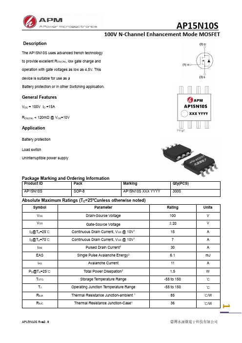
Typical Characteristics
ID Drain Current (A)
15
96
VGS=10V
12
VGS=7V
VGS=5V
94
VGS=4.5V
9
RD S O (N m Ω )
92
6
VGS=3V
ID= 2 A
90 3
IAS
Avalanche Current
PD@TA=25℃
Total Power Dissipation3
TSTG
Storage Temperature Range
TJ
Operating Junction Temperature Range
RθJA
Thermal Resistance Junction-ambient 1
General Features
VDS = 100V ID =15A RDS(ON) < 120mΩ @ VGS=10V
Application
Battery protection Load switch Uninterruptible power supply
Package Marking and Ordering Information
BVDSS Drain-Source Breakdown Voltage △BVDSS/△TJ BVDSS Temperature Coefficient
RDS(ON) Static Drain-Source On-Resistance2
VGS=0V , ID=250uA Reference to 25℃ , ID=1mA VGS=10V , ID=2A VGS=4.5V , ID=1A
呼吸机专用mos管 AP15N10D 15A 100V TO-252

1DescriptionThe AP15N10D uses advanced trench technology and design to provide excellent R DS(ON) with low gat e charge. It can be used in a wide variety of applications. It is ESD protested.General FeaturesV DS =100V,I D =15AR DS(ON) <112m Ω @ V GS =10VApplicationPower switch DC/DC convertersCElectrical Characteristics (T J=25℃, unless otherwise noted)V DD=50V , V GS=10V ,R G=3.3I D=10A1.The data tested by surface mounted on a 1 inch2 FR-4 board with 2OZ copper.2.The data tested by pulsed , pulse width ≦ 300us , duty cycle ≦ 2%3.The EAS data shows Max. rating . The test condition is V DD=25V,V GS=10V,L=0.1mH,I AS=11A4.The power dissipation is limited by 150℃ junction temperature5.The data is theoretically the same as I D and I DM , in real applications , should be limited by total power dissipation.23150Typical Characteristics Fig.1 Typical Output Characteristics Fig.2 On-Resistance vs. Gate-Source Fig.3 Forward Characteristics Of Reverse Fig.4 Gate-Charge Characteristics Fig.5 Normalized V vs. T4I AS V GS BV DSSV DD EAS=12L x I AS 2 x BV DSSBV DSS -V DDFig.8 Safe Operating AreaFig.7 Capacitance Fig.10 Switching Time Waveform Fig.11 Unclamped Inductive Switching Waveform5Package Mechanical DataDimensionsMillimeters Inches Ref.Min.Typ.Max.Min.Typ.Max.A A2B C DE G H LV1V22.1000.660.40 2.500.100.860.600.08300.0260.0160.0980.0040.0340.0246.409.5010.700.3740.4210.0530.0655.906.30L20°6°0.2320.2486.800.2520.2684.47 4.670.1760.1841.09 1.210.0430.0487°1.351.650°6°7°B2 5.18 5.480.2020.216C20.440.580.0170.023D1E15.30REF4.630.1820.209REFDETAIL ATO-252Reel Spectification-TO-252ABBDimensionsMillimeters Inches Ref.Min.Typ.Max.Min.Typ.Max.W E F D0D1P0P1P2A0B0K0T t115.901.657.401.4016.101.857.601.600.6260.0650.2910.0550.6340.0730.2990.0631.40 1.607.9010.4510.600.4110.4170.240.270.0090.0110.0550.0633.90 4.106.900.27110P00.1540.1618.100.3110.3191.90 2.100.0750.0830.100.00440.001.5752.780.10916.001.757.501.501.504.008.002.0010.500.6300.0690.2950.0590.0590.1570.3150.0790.4136.857.002.68 2.880.2700.2760.1050.11339.8040.201.5671.583Attention1,Any and all APM Microelectronics products described or contained herein do not have specificationsthat can handle applications that require extremely high levels of reliability, such as life support systems, aircraft's control systems, or other applications whose failure can be reasonably expected to result inserious physical and/or material damage. Consult with your APM Microelectronics representative nearestyou before using any APM Microelectronics products described or contained herein in such applications.2,APM Microelectronics assumes no responsibility for equipment failures that result from using productsat values that exceed, even momentarily, rated values (such as maximum ratings, operating condition ranges, or other parameters) listed in products specifications of any and all APM Microelectronicsproducts described or contained herein.3, Specifications of any and all APM Microelectronics products described or contained here instipulate the performance, characteristics, and functions of the describ ed products in the independent state, and arenot guarantees of the performance, characteristics, and functions of the described products as mountedin the customer’s products or equipment. To verify symptoms and states that cannot be evaluated in an independent device, the customer should always evaluate and test devices mounted in the customer’s products or equipment.4, APM Microelectronics Semiconductor CO., LTD. strives to supply high quality high reliability products. However, any and all semiconductor products fail with some probability. It is possible that theseprobabilistic failures could give rise to accidents or events that could endanger human lives that couldgive rise to smoke or fire, or that could cause damage to other property. When designing equipment,adopt safety measures so that these kinds of accidents or events cannot occur. Such measures includebut are not limited to protective circuits and error prevention circuits for safe design, redundantdesign,and structural design.5,In the event that any or all APM Microelectronics products(including technical data, services) describedor contained herein are controlled under any of applicable local export control laws and regulations, such products must not be exported without obtaining the export license from the authorities concerned in accordance with the above law.6, No part of this publication may be reproduced or transmitted in any form or by any means,electronic or mechanical, including photocopying and recording, or any information storage or retrieval system, or otherwise, without the prior written permission of APM Microelectronics Semiconductor CO., LTD.7, Information (including circuit diagrams and circuit parameters) herein is for example only; it is not guaranteed for volume production. APM Microelectronics believes information herein is accurate andreliable, but no guarantees are made or implied regarding its use or any infringements of intellectualproperty rights or other rights of third parties.8, Any and all information described or contained herein are subject to change without notice due toproduct/technology improvement,etc. When designing equipment, refer to the "Delivery Specification" forthe APM Microelectronics product that you Intend to use.6。
呼吸机专用mos管APG60N12PT 60A 120V TO-220 TO-263
APG60N12P I T120V N-SGT Enhancement Mode MOSFET1General DescriptionAPG60N12P/T use advanced SGT MOSFET technology to provide low RDS(ON), low gate charge, fast switching This device is specially designed to get better ruggednessand suitable to use inFeaturesLow RDS(on) & FOMExtremely low switching lossExcellent stability and uniformity or InvertorsApplicationsConsumer electronic power supply Motor controlSynchronous-rectification Isolated DC Synchronous-rectification applicationsProduct ID Pack MarkingQty(PCS) APG60N12P TO-220-3L APG60N12P XXX YYYY 1000 APG60N12TTO-263-3LAPG60N12T XXX YYYY1000Absolute Maximum Ratings at T j =25℃ unless otherwise notedParameterSymbol Value Unit Drain source voltage V DS 120 V Gate source voltageV GS ±20 V Continuous drain current 1), T C =25 ℃ I D 60 A Pulsed drain current 2), T C =25 ℃ I D, pulse 180 A Power dissipation 3), T C =25 ℃ P D 33 W Single pulsed avalanche energy 5) E AS 100 mJ Operation and storage temperature T stg ,T j -55 to 150℃ Thermal resistance, junction-case R θJC 3.8 ℃/W Thermal resistance, junction-ambient 4)R θJA62.5℃/W2Electrical Characteristics at T j =25 ℃ unless otherwise specifiedParameterSymbolMin. Typ. Max. Unit Test condition Drain-source breakdown voltage BV DSS 120 V V GS =0 V, I D =250 μA Gate threshold voltage V GS(th) 1.5 2.5 V V DS =V GS , I D =250 μA Drain-source on-state resistanceR DS(ON)10.6 13 mΩV GS =10 V, I D =30 A Gate-source leakage current I GSS100 nA V GS =20 V-100V GS =-20 V Drain-source leakage current I DSS 1 μA V DS =120 V, V GS =0 V Input capacitance C iss 2809.7 pF V GS =0 V, V DS =50 V, ƒ=100 kHz Output capacitance C oss 356.1 pF Reverse transfer capacitance C rss 8.3 pF Turn-on delay time t d(on) 20.4 ns V GS =10 V, V DS =50 V, R G =2 Ω, I D =25 ARise time t r 5.7 ns Turn-off delay time t d(off) 45.1 ns Fall time t f 6.3 ns Total gate charge Q g 39.6 nC I D =25 A, V DS =50 V, V GS =10 V Gate-source charge Q gs 6.8 nC Gate-drain charge Q gd 8.0 nC Gate plateau voltage V plateau 3.5 V Diode forward current I S 60 AV GS <V th Pulsed source current I SP 180Diode forward voltage V SD 1.3 V I S =60 A, V GS =0 V Reverse recovery time t rr 79.5 ns I S =25 A, di/dt=100 A/μsReverse recovery charge Q rr 210 nC Peak reverse recovery currentI rrm4.4AElectrical Characteristics Diagrams34◼Test circuits and waveformsFigure 1,G ate c h arge t e st c i rcuit & w a veformFigure , 2S w itching t ime t e st c i rcuit & w a veformsFigure , 3Unclamped i n ductive s w itching (UIS) t e st c i rcuit & w a veformsFigure 4, Diode reverse recovery test circuit & waveforms56Attention1,Any and all APM Microelectronics products described or contained herein do not have specificationsthat can handle applications that require extremely high levels of reliability, such as life support systems, aircraft's control systems, or other applications whose failure can be reasonably expected to result inserious physical and/or material damage. Consult with your APM Microelectronics representative nearestyou before using any APM Microelectronics products described or contained herein in such applications.2,APM Microelectronics assumes no responsibility for equipment failures that result from using productsat values that exceed, even momentarily, rated values (such as maximum ratings, operating condition ranges, or other parameters) listed in products specifications of any and all APM Microelectronicsproducts described or contained herein.3, Specifications of any and all APM Microelectronics products described or contained here instipulate the performance, characteristics, and functions of the describ ed products in the independent state, and arenot guarantees of the performance, characteristics, and functions of the described products as mountedin the customer’s products or equipment. To verify symptoms and states that cannot be evaluated in an independent device, the customer should always evaluate and test devices mounted in the customer’s products or equipment.4, APM Microelectronics Semiconductor CO., LTD. strives to supply high quality high reliability products. However, any and all semiconductor products fail with some probability. It is possible that theseprobabilistic failures could give rise to accidents or events that could endanger human lives that couldgive rise to smoke or fire, or that could cause damage to other property. When designing equipment,adopt safety measures so that these kinds of accidents or events cannot occur. Such measures includebut are not limited to protective circuits and error prevention circuits for safe design, redundantdesign,and structural design.5,In the event that any or all APM Microelectronics products(including technical data, services) describedor contained herein are controlled under any of applicable local export control laws and regulations, such products must not be exported without obtaining the export license from the authorities concerned in accordance with the above law.6, No part of this publication may be reproduced or transmitted in any form or by any means,electronic or mechanical, including photocopying and recording, or any information storage or retrieval system, or otherwise, without the prior written permission of APM Microelectronics Semiconductor CO., LTD.7, Information (including circuit diagrams and circuit parameters) herein is for example only; it is not guaranteed for volume production. APM Microelectronics believes information herein is accurate andreliable, but no guarantees are made or implied regarding its use or any infringements of intellectualproperty rights or other rights of third parties.8, Any and all information described or contained herein are subject to change without notice due toproduct/technology improvement,etc. When designing equipment, refer to the "Delivery Specification" forthe APM Microelectronics product that you Intend to use.7。
呼吸机专用mos管 AP30P06D -30A -60V TO-252

1DESCRIPTIONThe AP30P06D uses advanced trench technology to provide excellent R DS(ON) and low gate charge .This device is suitable for use as a load switch or in PWM applications. GENERAL FEATURES V DS =- 60V,I D =-30A R DS(ON) < 40mΩ @ V GS =-10V R DS(ON) < 55mΩ @ V GS =-4.5VHigh Power and current handing capability Lead free product is acquired Surface Mount Package Application PWM applications Load switch Power managementParameter Symbol Condition Min Typ Max Unit Drain-Source Breakdown Voltage BV DSS V GS=0V I D=-250μA -60 V Zero Gate Voltage Drain Current I DSS V DS=-48V,V GS=0V -1 μA Gate-Body Leakage Current I GSS V GS=±20V,V DS=0V ±100 nA Gate Threshold Voltage V GS(th)V DS=V GS,I D=-250μA -1 -1.8 -2.5 VDrain-Source On-State Resistance R DS(ON)V GS=-10V, I D=-20A 31 40 mΩ V GS=-4.5V, I D=-20A 42 55 mΩForward Transconductance g FS V DS=-5V,I D=-20A 5 SInput Capacitance C lssV DS=-30V,V GS=0V,F=1.0MHz 3060 PFOutput Capacitance C oss300 PF Reverse Transfer Capacitance C rss205 PFTurn-on Delay Time t d(on)V DS=-30V,V GS=-10V,R GEN=3ΩI D=1A 14 nSTurn-on Rise Time t r20 nS Turn-Off Delay Time t d(off)40 nS Turn-Off Fall Time t f19 nST otal Gate Charge Q gV DS=-30V,I D=-20A,V GS=-10V 48 nCGate-Source Charge Q gs11 nCGate-Drain Charge Q gd10 nCBody Diode Reverse Recovery Time T rrI F=-20A, dI/dt=100A/µs40 nSBody Diode Reverse Recovery Charge Q rr56 nCDiode Forward Voltage (Note 3) V SD V GS=0V,I S=-1A -0.72 -1 VNOTES:1. Repetitive Rating: Pulse width limited by maximum junction temperature.2. Surface Mounted on 1in2 FR4 Board, t ≤ 10 sec.3. Pulse T est: Pulse Width ≤ 300μs, Duty Cycle ≤ 2%.4. Guaranteed by design, not subject to production testing.23TYPICAL ELECTRICAL AND THERMAL CHARACTERISTICSV INV t Figure 2:Switching WaveformsFigure 1:Switching Test CircuitFigure 3 Power DissipationT J -Junction Temperature(℃) P D P o w e r (W )D - D r a i n C u r r e n t (A )-I T J -Junction Temperature(℃)Figure 4 Drain Current-I D R d s o n O n -R e s i s t a n c e (m Ω)- D r a i n C u r r e n t (A )-I -Vds Drain-Source Voltage (V) D - Drain Current (A)Figure 6 Drain-Source On-ResistanceFigure 5 Output CHARACTERISTICS4-IN o r m a l i z e d O n -R e s i s t a n c eD - D r a i n C u r r e n t (A )-Vgs Gate-Source Voltage (V)T J -Junction Temperature(℃)Figure 7 Transfer Characteristics Figure 8 Drain-Source On-ResistanceR d s o n O n -R e s i s t a n c e (m Ω)C C a p a c i t a n c e (p F )-Vgs Gate-Source Voltage (V)-Vds Drain-Source Voltage (V)Figure 10 Capacitance vs VdsFigure 9 Rdson vs Vgs-V g s G a t e -S o u r c e V o l t a g e (V )s - R e v e r s e D r a i n C u r r e n t (A )-I Qg Gate Charge (nC)-Vsd Source-Drain Voltage (V)Figure 11 Gate ChargeFigure 12 Source- Drain Diode Forward5D - D r a i n C u r r e n t (A )-IVds Drain-Source Voltage (V)Figure 13 Safe Operation AreaSquare Wave Pluse Duration(sec)Figure 14 Normalized Maximum Transient Thermal ImpedanceZ t h J A N o r m a l i z e d T r a n s i e n t T h e r m a l R e s i s t a n ceTO-252 Package InformationSymbolDimensions In Millimeters Dimensions In Inches Min.Max.Min.Max.A 2.200 2.400 0.087 0.094A1 0.000 0.127 0.000 0.005b 0.660 0.860 0.026 0.034c 0.460 0.580 0.018 0.023D 6.500 6.700 0.256 0.264D1 5.100 5.460 0.201 0.215D2 4.830 TYP. 0.190 TYP.E 6.000 6.200 0.236 0.244e 2.186 2.386 0.086 0.094L 9.800 10.400 0.386 0.409L1 2.900 TYP. 0.114 TYP.L21.400 1.700 0.055 0.067L3 1.600 TYP. 0.063 TYP.L4 0.600 1.000 0.024 0.039Φ 1.100 1.300 0.043 0.051θ 0°8°0°8°h 0.000 0.300 0.000 0.012V 5.350 TYP. 0.211 TYP.6Attention1,Any and all APM Microelectronics products described or contained herein do not have specifications that can handle applications that require extremely high levels of reliability, such as life support systems, aircraft's control systems,or other applications whose failure can be reasonably expected to result in serious physical and/or materialdamage. Consult with your APM Microelectronics representative nearest you before using any APMMicroelectronics products described or contained herein in such applications.2,APM Microelectronics assumes no responsibility for equipment failures that result from using products at values that exceed, even momentarily, rated values (such as maximum ratings, operating condition ranges, or otherparameters) listed in products specifications of any and all APM Microelectronics products described or containedherein.3, Specifications of any and all APM Microelectronics products described or contained here instipulate the performance, characteristics, and functions of the described products in the independent state, and are not guarantees of theperformance, characteristics, and functions of the described products as mounted in the customer’s products orequipment. T o verify symptoms and states that cannot be evaluated in an independent device, the customer shouldalways evaluate and test devices mounted in the customer’s products or equipment.4, APM Microelectronics Semiconductor CO., LTD. strives to supply high quality high reliability products. However, any and all semiconductor products fail with some probability. It is possible that these probabilistic failures could giverise to accidents or events that could endanger human lives that could give rise to smoke or fire, or that couldcause damage to other property. When designing equipment, adopt safety measures so that these kinds ofaccidents or events cannot occur. Such measures include but are not limited to protective circuits and errorprevention circuits for safe design, redundant design,and structural design.5,In the event that any or all APM Microelectronics products(including technical data, services) described or contained herein are controlled under any of applicable local export control laws and regulations, such products must not beexported without obtaining the export license from the authorities concerned in accordance with the above law.6, No part of this publication may be reproduced or transmitted in any form or by an y means,electronic or mechanical, including photocopying and recording, or any information storage or retrieval system, or otherwise, without theprior written permission of APM Microelectronics Semiconductor CO., LTD.7, Information (including circuit diagrams and circuit parameters) herein is for example only; it is not guaranteed for volume production. APM Microelectronics believes information herein is accurate and reliable, but no guaranteesare made or implied regarding its use or any infringements of intellectual property rights or other rights of thirdparties.8, Any and all information described or contained herein are subject to change without notice due to product/technology improvement,etc. When designing equipment, refer to the "Delivery Specification" for the APM Microelectronicsproduct that you Intend to use.9, this catalog provides information as of Sep.2014. Specifications and information herein are subject to change without notice7。
呼吸机专用mos管 AP15P04D -15A -40V TO-252

40V P-Channel Enhancement Mode MOSFET1General DescriptionThe AP15P04D uses advanced trench technology to provide excellent R DS(ON), low gate charge and operation with gate voltages as low as -4.5V. This device is suitable for use as a wide variety of applications.FeaturesV DS = -40V,ID =-15AR DS(ON) < 36mΩ @ V GS =-10V R DS(ON) < 52mΩ @ V GS =-4.5VHigh Power and current handing capability Lead free product is acquired Surface Mount PackageApplicationPWM applications Load switchPower managementAbsolute Maximum Ratings (T A =25℃)40V P-Channel Enhancement Mode MOSFET2RJCThermal Resistance,Junction-to-Case4℃/WElectrical Characteristics (TA=25℃unless otherwise noted)Symbol ParameterConditionsMin Typ Max Unit BV DSS Drain-Source Breakdown VoltageV GS =0V I D =-250μA -40V I DSS Zero Gate Voltage Drain Current V DS =-32V,V GS =0V -1 μA I GSS Gate-Body Leakage Current V GS =±20V,V DS =0V ±100 nA V GS(th) Gate Threshold Voltage V DS =V GS ,I D =-250μA -1 -2 -3 V g FS Forward Transconductance V DS =-5V,I D =-10A 25 S R DS(ON)Drain-Source On-State ResistanceV GS =-10V, I D =-20A 2536 mΩV GS =-4.5V, I D =-10A42 52 mΩ C issInput Capacitance V DS =-25V,V GS =0V,f=1.0MHz840 pF C oss Output Capacitance 92 pF C rss Reverse Transfer Capacitance 60 pF t d(on) Turn-on Delay Time V GS =-10V, V DS =-20V, R L =1.6,R GEN =35 nS t r Turn-on Rise Time 12 nS t d(off) Turn-Off Delay Time 20 nS t f Turn-Off Fall Time 4.5 nS Q g Total Gate Charge V GS =-10V, V DS =-20V, I D =-15A20 nC Q gs Gate-Source Charge 2.5 nC Q gd Gate-Drain Charge4.5 nC I SD Source-Drain Current(Body Diode) -20 A V SDForward on VoltageV GS =0V,I S =-20A-1.2V40V P-Channel Enhancement Mode MOSFET3Switch Time Test Circuit and Switching Waveforms :TYPICAL ELECTRICAL AND THERMAL CHARACTERISTICS (Curves)Figure1. Power DissipationFigure2. Drain CurrentFigure3. Output CharacteristicsFigure4. Transfer Characteristics-I D D r a i n C u r r e n t (A )T J -Junction Temperature(℃)P o w e r D i s s i p a t i o n (W )T J -Junction Temperature(℃)40V P-Channel Enhancement Mode MOSFET4Figure5. Capacitance Figure6. R DS(ON) vs Junction TemperatureFigure7. V GS(th) vs Junction TemperatureFigure8. Gate Charge WaveformsFigure9. Normalized Maximum Transient Thermal ImpedanceC C a p a c i t a n c e (pF )-VDS Drain-to-Source Voltage(V) -V g s (V )Qg(nC)40V P-Channel Enhancement Mode MOSFETTO-252 Package Information540V P-Channel Enhancement Mode MOSFETAttention1,Any and all APM Microelectronics products described or contained herein do not have specificationsthat can handle applications that require extremely high levels of reliability, such as life support systems, aircraft's control systems, or other applications whose failure can be reasonably expected to result in serious physical and/or material damage. Consult with your APM Microelectronics representative nearest you before using any APM Microelectronics products described or contained herein in such applications. 2,APM Microelectronics assumes no responsibility for equipment failures that result from using productsat values that exceed, even momentarily, rated values (such as maximum ratings, operating condition ranges, or other parameters) listed in products specifications of any and all APM Microelectronics products described or contained herein.3, Specifications of any and all APM Microelectronics products described or contained here instipulate the performance, characteristics, and functions of the described products in the independent state, and arenot guarantees of the performance, characteristics, and functions of the described products as mountedin the customer’s products or equipment. To verify symptoms and states that cannot be evaluated in an independent device, the customer should always evaluate and test devices mounted in the customer’s products or equipment.4, APM Microelectronics Semiconductor CO., LTD. strives to supply high quality high reliability products. However, any and all semiconductor products fail with some probability. It is possible that these probabilistic failures could give rise to accidents or events that could endanger human lives that couldgive rise to smoke or fire, or that could cause damage to other property. When designing equipment, adopt safety measures so that these kinds of accidents or events cannot occur. Such measures include but are not limited to protective circuits and error prevention circuits for safe design, redundantdesign,and structural design.5,In the event that any or all APM Microelectronics products(including technical data, services) described or contained herein are controlled under any of applicable local export control laws and regulations, such products must not be exported without obtaining the export license from the authorities concerned in accordance with the above law.6, No part of this publication may be reproduced or transmitted in any form or by any means,electronic or mechanical, including photocopying and recording, or any information storage or retrieval system, or otherwise, without the prior written permission of APM Microelectronics Semiconductor CO., LTD.7, Information (including circuit diagrams and circuit parameters) herein is for example only; it is not guaranteed for volume production. APM Microelectronics believes information herein is accurate and reliable, but no guarantees are made or implied regarding its use or any infringements of intellectual property rights or other rights of third parties.8, Any and all information described or contained herein are subject to change without notice due to product/technology improvement,etc. When designing equipment, refer to the "Delivery Specification" for the APM Microelectronics product that you Intend to use.6。
- 1、下载文档前请自行甄别文档内容的完整性,平台不提供额外的编辑、内容补充、找答案等附加服务。
- 2、"仅部分预览"的文档,不可在线预览部分如存在完整性等问题,可反馈申请退款(可完整预览的文档不适用该条件!)。
- 3、如文档侵犯您的权益,请联系客服反馈,我们会尽快为您处理(人工客服工作时间:9:00-18:30)。
Millimeters
Inches
Min. Typ. Max. Min. Typ. Max.
A
2.10
2.50 0.083
0.098
A2
0
0.10
0
0.004
B
0.66
0.86 0.026
0.034
B2 5.18
5.48 0.202
0.216
C
0.40
0.60 0.016
0.024
C2 0.44
0.58 0.017
150
Fig.5 Normalized VGS(th) v.s TJ
AP15P06D Rve3.9
Fig.4 Gate-Charge Characteristics
2.5
2.0
1.5
1.0
0.5 -50
0
50
100
150
TJ , Junction Temperature ( )
Fig.6 Normalized RDSON v.s TJ
Typical Characteristics
AP15P06D
-60V P-Channel Enhancement Mode MOSFET
Fig.3 Forward Characteristics of Reverse
1.5
1
0.5
0
-50
TJ
0
,Junction
50
Temperature
(oC)100
---
5
uA
IGSS
Gate-Source Leakage Current
VGS=±20V , VDS=0V
---
--- ±100 nA
gfs
Forward Transconductance
VDS=-5V , ID=-12A
--- 15.4 ---
S
Rg
Gate Resistance
VDS=0V , VGS=0V , f=1MHz
TSTG
Storage Temperature Range
TJ
Operating Junction Temperature Range
RθJA
Thermal Resistance Junction-Ambient 1
RθJC
Thermal Resistance Junction-Case1
Rating -60 ±20 -15 -11 -4.3 -3.5 -36 35.4 -26.6 34.7 2
Product ID
Pack
Marking
Qty(PCS)
AP15P06D
TO-252-2
AP15P06D XXX YYYY
2500
Absolute Maximum Ratings (TA=25℃unless otherwise noted)
Symbol
Parameter
VDS
Drain-Source Voltage
Description
AP15P06D
-60V P-Channel Enhancement Mode MOSFET
The AP15P06D uses advanced trench technology to provide excellent RDS(ON), low gate charge and operation with gate voltages as low as 4.5V. This device is suitable for use as a Battery protection or in other Switching application.
0.023
B
C
G
DETAIL A
V1
D
5.90
6.30 0.232
0.248
D1
5.30REF
0.209REF
E
6.40
6.80 0.252
0.268
E1 4.63
0.182
G
4.47
4.67 0.176
0.184
H
9.50
10.70 0.374
0.421
L
1.09
V1
L2 1.35
1.21 0.043 1.65 0.053
1.575 1.583
AP15P06D Rve3.9
臺灣永源微電子科技有限公司
AP15P06D
-60V P-Channel Enhancement Mode MOSFET
Attention
1,Any and all APM Microelectronics products described or contained herein do not have specifications that can handle applications that require extremely high levels of reliability, such as life support systems, aircraft's control systems, or other applications whose failure can be reasonably expected to result in serious physical and/or material damage. Consult with your APM Microelectronics representative nearest you before using any APM Microelectronics products described or contained herein in such applications.
---
13.5
---
Ω
Qg
Total Gate Charge (-4.5V)
--- 9.86 ---
Qgs
Gate-Source Charge
VDS=-48V , VGS=-4.5V , ID=-10A ---
3.08
---
nC
Qgd
Gate-Drain Charge
--- 2.95 ---
Td(on)
臺灣永源微電子科技有限公司
3
AP15P06D
-60V P-Channel Enhancement Mode MOSFET
Fig.9 Normalized Maximum Transient Thermal Impedance
Fig.10 Switching Time Waveform AP15P06D Rve3.9
Dimensions
Millimeters
Min. Typ. Max. Min.
15.90 16.00 16.10 0.626
1.65 1.75 1.85 0.065
7.40 7.50 7.60 0.291
1.40 1.50 1.60 0.055
1.40 1.50 1.60 0.055
3.90 4.00 4.10 0.154
Fig.11 Unclamped Inductive Waveform 臺灣永源微電子科技有限公司
4
5
V1 V2
Package Mechanical Data
AP15P06D
-60V P-Channel Enhancement Mode MOSFET
H L
D
E
A
Dimensions
B2
C2
Ref.
---
---
-18
A
ISM
Pulsed Source Current2,5
VG=VD=0V , Force Current
---
---
-36
A
VSD
Diode Forward Voltage2
VGS=0V , IS=-1A , TJ=25℃
---
--- -1.2
V
Note : 1.The data tested by surface mounted on a 1 inch2 FR-4 board with 2OZ copper. 2.The data tested by pulsed , pulse width ≦ 300us , duty cycle ≦ 2%
Ciss
Input Capacitance
---
1447 ---
Coss
Output Capacitance
VDS=-15V , VGS=0V , f=1MHz ---
97.3
---
pF
Crss
Reverse Transfer Capacitance
---
70
---
IS
Continuous Source Current1,5
-55 to 150 -55 to 150
62 3.6
Units V V A A A A A mJ A W W ℃ ℃
℃/W ℃/W
1
AP15P06D Rve3.9
臺灣永源微電子科技有限公司
AP15P06D
-60V P-Channel Enhancement Mode MOSFET
Electrical Characteristics (TA=25℃unless otherwise noted)
5.The data is theoretically the same as ID and IDM , in real applications , should be limited by total power dissipation.