PK25F40中文资料
CC2540、BLE、低功耗蓝牙4.0、透传模块-硬件手册

MT254xCoreS 硬件手册V1.0深圳市馒头科技有限公司产品型号说明馒头科技缩写版本编号直插; Board-底板版本更新记录目录第1章产品介绍 (5)1.1蓝牙4.0介绍 (5)1.2MT254xCoreS介绍 (5)第2章硬件资源 (6)2.1晶振 (6)2.2天线 (6)2.3电阻电容 (6)2.4对外接口 (6)第3章技术规格说明 (7)3.1外观尺寸 (7)3.2引脚分布图 (7)3.3引脚功能说明 (8)第4章开发事项 (9)4.1模块透传功能 (9)4.2BLE协议栈开发 (9)4.3IO复用功能表 (10)附录A 模块实物图 (12)第1章产品介绍1.1 蓝牙4.0介绍蓝牙4.0是2012年最新蓝牙版本,是3.0的升级版本;较3.0版本更省电、成本低、3毫秒低延迟、超长有效连接距离、AES-128加密等;通常用在蓝牙耳机、蓝牙音箱等设备上。
蓝牙4.0最重要的特性是省电,极低的运行和待机功耗可以使一粒纽扣电池连续工作数年之久。
此外,低成本和跨厂商互操作性,3毫秒低延迟、AES-128加密等诸多特色,可以用于计步器、心律监视器、智能仪表、传感器物联网等众多领域,大大扩展蓝牙技术的应用范围。
蓝牙4.0已经走向了商用,在最新款的Xperia Z、Galaxy S3、S4、Note2、SurfaceRT、iPhone 5、iPhone 4S、魅族MX3、Moto Droid Razr、HTC One X、小米手机2、The New iPad、iPad 4、MacBook Air、Macbook Pro,Nokia Lumia系列以及台商ACER AS3951系列/Getway NV57系列,ASUS UX21/31三星NOTE系列上都已应用了蓝牙4.0技术。
蓝牙4.0支持两种部署方式:双模式和单模式。
双模式中,低功耗蓝牙功能集成在现有的经典蓝牙控制器中,或再在现有经典蓝牙技术(2.1+EDR/3.0+HS)芯片上增加低功耗堆栈,整体架构基本不变,因此成本增加有限。
美国AMC伺服驱动器25A8中文产品技术资料

零漂调节/测试。用来调节任何输入信号或者驱动器内部的零漂。也可以作为内
4
负向调整零漂
部信号源,用来实现测试的目的。
注意:电位器近似是线性的,一共 12 圈,头尾各 1 圈是无效的。
电位器调节方法(摘自 instnotes)
n Offet(l 零漂调节) 在调节零漂之前,参考输入(Reference Input)引脚必须接地或者输入的指令电压为零伏。先把测试/
*Approvals may be pending. See “Compliances & Agency Approvals” on page 1 of datasheet for currently held approvals.
上海同普电力技术有限公司 地址:上海市杨浦区赤峰路 65 号 1 号楼
功能结构图
25A8
模式选择表
SW1 SW2 SW3
电流模式
OFF OFF ON
电压模式
ON OFF OFF
IR 补偿模式
ON OFF OFF
测速发电机模式 OFF OFF OFF
大多数应用场合 SW2 都应该是 OFF。
绿色 LED 指示灯:工作正常 红色 LED 指示灯:故障状态 电流模式下的推荐设置:POT1 逆时针最大,POT3 顺时针最大 驱动器出厂时为电流模式且限制电流最大 其他拨码开关的功能请参看拨码开关介绍部分 *由用户选择安装的通孔器件
RoHS (Reduction of Hazardous Substances) is intended to prevent hazardous substances such as lead from beingmanufactured in electrical and electronic equipment.
FM25F02.04使用说明手册

FM25F04/02使用手册1.产品概述FM25F04/02为4M/2M位的串行Flash存储器,内部组织为524,288个字节(FM25F04)/262144个字节(FM25F02),另外还有一个256字节的OTP扇区,每个字节8位。
芯片接口为兼容SPI协议(模式3/0)的串行接口总线,广泛应用于消费类电子市场。
主要用于存储固件和配置、设置信息。
产品的基本性能如下:✧工作电压:2.3V - 3.6V✧统一扇区架构:-128个4-Kbyte扇区(FM25F04),64个4-Kbyte扇区(FM25F02)-8个64K-byte区块(FM25F04),4个64K-byte区块(FM25F02)-任意扇区或区块都可以被单独擦除✧可锁定的256 byte OTP安全扇区✧SPI串行接口(模式0及模式3)✧支持Dual Output Fast Read操作✧支持Dual I/O Fast Read操作,在此操作下也支持Continuous Read✧支持软/硬件写保护✧支持256字节页编程模式Manu ID:A1JEDEC ID:A13112(FM25F02),A13113(FM25F04)2.引脚定义FM25F04/023.直流参数(TA=-40℃~85℃,Vcc=2.3V~3.6V)f CLK=100MHZ时CL=20 pF, f CLK=75MHZ时CL=30 pF5.上电时序上电时序及写禁止电压FM25F04/02状态寄存器定义注意:1.在OTP模式下,SRP位定义为OTP_LOCK位2.见"保护区域表”7.操作命令说明所有的命令、地址和数据都是移位进出芯片,最高位(MSB)在第一位。
DI在CS#为低后的第一个CLK的上升沿被采样,之后,一字节的命令码必须被移位输入芯片,最高位在第一位,每位都在时钟的上升沿被采样。
下表列出了命令集。
每种命令序列都由一个单字节命令码开始。
根据不同的命令,后面跟随的可能是地址字节或数据字节,或什么都不跟。
PK25F160中文资料
Ratings 10 10 1.55 50/3 0.25 10 500 50 100 0.78
Unit mA mA V mA/V V s V/ s mA mA /W
mark Thyristor and Diode part. No mark
SanRex 50 Seaview Blvd. Port Washington, NY 11050-4618 PH.(516)625-1313 FAX(516)625-8845 E-mail: semi@
V V V Unit A A A A2S W W A V V A/ s V
Conditions Single phase, half wave, 180 conduction, Tc 96 Single phase, half wave, 180 conduction, Tc 96 1 cycle, 50Hz/60Hz, peak Value, non-repetitive 2 Value for one cycle of surge current
;;
元器件交易网
PK(PD,PE,KK)25F
VRRM VRSM VDRM Symbol IT AV IT RMS ITSM I2t PGM PG AV IFGM VFGM VRGM di dt VISO Tj Tstg
6.5 29max
Unit A
3.5
7.5 3.5
2- 6
20
20
92 20
17.5
Repetitive Peak Reverse Voltage Non-Repetitive Peak Reverse Voltage Repetitive Peak Off-State Voltage Item Average On-State Current R.M.S. On-State Current Surge On-State Current I2t Peak Gate Power Dissipation verage Gate Power Dissipation Peak Gate Current Peak Gate Voltage (Forward) Peak Gate Voltage (Reverse) Critical Rate of Rise of On-State Current Isolation Breakdown Voltage (R.M.S.) Operating Junction Temperature Storage Temperature Mounting M5 Mounting Torque Terminal M5 Mass
MF-25中文资料
MF-SERIESGENERAL PURPOSE METAL FILM RESISTORS Small SizePRODUCT BULLETIN REV C12/27/99Continued on reverse sideWILLOW TECHNOLOGIES LTD.SHAWLANDS COURT, NEWCHAPEL ROAD LINGFIELD, SURREY, RH7 6BL, ENGLANDTel. + 44 (0) 1342 835234 Fax. + 44 (0) 1342 834306E-mail rob@ Website REV D 1/20/99Characteristic Specificati on Test Method(All resistance measurements should be performed after stabilization or conditioning periods.) DC RESISTANCE Within specifiedtolerance.MIL-STD-202Method 303 TEMPERATURE COEFFICIENT As buyer requested±25PPM/°C ±100PPM/°C ±50PPM/°C ±200PPM/°C MIL-STD-202 Method 304DIELECTRIC STRENGTHNo flashover or damageMIL-STD-202 Method 3011/8W 300V 1 minute 1/4W 500V 1 minute 1/2W 700V 1 minute 1, 2W 750V 1 minute INSULATION RESISTANCE At least 1000M ΩMIL-STD-202 Method 302 100V 1 minute CURRENT NOISE TEST 5.11Ω to 9.99Ω less than 0.05µV/V10Ω to 9.99K Ω less then 0.1µV/V 10K Ω to 1M Ω less then 0.2µV/V MIL-STD-202 Method 308VIBRATION∆R within ±(0.25% + 0.05Ω)MIL-STD-202 Method 201 10~ HzX.Y.Z. 3 directions 2 hours each. TERMINAL STRENGTHNo broken or loosened terminals.MIL-STD-202 Method 211 RESISTANCE TO SOLDERING HEAT ∆R within ±(0.25% + 0.05Ω) MIL-STD-202 Method 210350°C, 3 ±0.05 seconds SOLDERABILITY At least 95% coverage MIL-STD-202 Method 208230°C, 5 seconds THERMAL SHOCK∆R within ±(0.5% + 0.05Ω)MIL-STD-202 Method 107 -55°C, +155°C 5 cyclesSHORT TIME OVERLOAD ∆R within ±(0.05% + 0.05Ω)MIL-R-10509 Para, 4.6.62.5 times rated working voltage, 5 seconds HUMIDITY∆R within ±(1% + 0.05Ω) NO mechanical damage MIL-STD-202 Method 10340°C, RH 95% 500 LOW TEMPERATURE OPERATION ∆R within ±(0.5% + 0.05Ω)MIL-R-10509 Para 4.6.5 Rated workingvoltage, @ -65°C 45 minutes. LOAD LIFE∆R within ±(1% + 0.05Ω)MIL-STD-202 Method 108 Rated workingVoltage 1 ½ hours on. ½ hour off for total 1000 hours RESISTANCE TO SOLVENT Color bands legible. No mechanical damage.MIL-STD-202 Method 2151.00.320.100.0320.0100.003101001K10K100K1M0-10-20-30-40-50Nominal Resistance (Ω)u V/VdBCURRENT NOISE。
PK40系列多通道信号隔离器说明书

PK40系列多通道信号隔离器使用说明书一、概述:PK-40系列信号隔离器用于对现场仪表的各类信号调整、隔离,并转换成计算机、DCS 、PLC 等能接受的标准信号或用户指定的特殊信号。
该隔离器输入、输出、电源三方全隔离隔离,抗干扰能力强,精度高,导轨安装。
具有极高的性价比,工作十分可靠和稳定,可以与单元组合仪表及DCS 、PLC 等系统配套使用,在油田、石化、制造、电力、冶金等行业的重大工程中有着广泛应用。
二、技术参数1.系统传输准确度:±0.2%×F ·S2.温度漂移:25ppm/℃3.输入阻抗:电流:250Ω;电压:500K Ω4.电流输出允许外接的负载阻抗:电流输出时<600Ω;典型负载为250 Ω。
电压输出允许外接负载>10K5.绝缘电阻:电源、输入、输出之间大于等于100M Ω(500VDC )6.输入/输出/电源隔离电压:≥3000V.dc/min7.供电电源:DC24V ±10%(反接保护)8.输入功率:<1W * N (N 为通道数)9.工作温度:工业级标准 -20~+70℃10.储运环境温度:-40~+85℃ 相对湿度:10-90%RH (40℃时)11.外形尺寸:长 x 宽 x 高 :71mm x 88mm x 62mm12.净 重:140g ±20g13. 安 装:35mm 标准导轨卡装三、隔离器引脚定义及接线示意图1. 隔离器外型示意图2.引脚定义及描述引脚号 信号输入描述 1+ 通道1信号输入正 2-Input(1)通道1信号输入负 5+ 通道2信号输入正 6-Input(2)通道2信号输入负 9+ 通道3信号输入正 10-Input(3)通道3信号输入负 13+ Output(1)通道1信号输出正 14-通道1信号输出负 17+ Output(2)通道2信号输出正 18-通道2信号输出负 21+ Output(3)通道3信号输出正 22-通道3信号输出负 23+ 24VDC 电源输入正 24-Power 24VDC 电源输入负注: 其他端子请勿接线四、使用环境安装位置不得有强烈振动,以及来自信号端、电源端及空间的超过EMC 标准的电磁冲击,并使用环境中不得有对金属、塑料件起严重腐蚀作用的有害物质。
24与25系列FLASH编程器说明
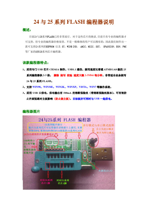
24与25系列FLASH编程器说明概述:目前24与25系列FLASH已经非常流行。
对于这些芯片的烧录,目前只有专业的编程器才可支持,但专业的编程器价格很贵,不是一般维修的用户可以拥有的;因此我们制作出一款可支持24系列的EEPROM 以及 ST,WINB IND, AMIC,MXIC,SST, SPANSION,EON,PMC 等厂家的8脚25系列芯片编程器。
该款编程器特点:1、采用专门USB芯片CH341A制作。
USB1.1通信。
烧写速度比普通ATMEGA8做的25系列编程器快2-3倍。
擦除烧写校验速度大概2-3Mbit每分钟。
非常适合业余烧写24与25系列FLASH。
2、支持WIN98,WINME,WIN2K,WINXP,VIST A,WIN7等操作系统。
3、采用USB口供电,供电输出有500mA的熔断保险丝(带熔断保险丝版本),可有效防止外面短路对主板影响(防止烧主板),目标板亦可同时与USB一起供电。
编程器图片驱动安装1:安装USB驱动(烧写24与25系列FLASH用到的驱动)将PCB板上P/S端跳帽合上详细安装步骤见”USB驱动自动安装”文件夹中图片说明2:安装TTL驱动(USB转串口,中九等支持串口在线下载的机型在线下载用)将PCB板上P/S端跳帽去掉详细安装步骤见”TTL驱动”文件夹中图片说明24系列芯片烧写(P/S端跳帽合上)1:放置芯片,如下图:2:将编程器插到电脑USB口,打开”USB口24-25系列编程器”或"LCDHome论坛_新版32M+USB口24-25系列编程器”中的烧写软件.选择好芯片的容量,即可烧写和擦除芯片.25系列芯片烧写(P/S端跳帽合上)1:放置芯片,如下图:2:将编程器插到电脑USB口,打开”USB口24-25系列编程器”或"LCDHome论坛_新版32M+USB口24-25系列编程器”中的烧写软件.选择好芯片的容量,即可烧写和擦除芯片.在线下载(USB转串口,P/S端跳帽断开)将编程器插到电脑USB口,编程器上的TX脚接到中九的RX,RX接到中九的TX,GND接到中九的GND.选择好对应的COM口,打开对应平台的下载软件,即可在线升级你的中九机了.附件(转换板焊接)TTL中九升级说明中九有TTL升级接口,电脑只有USB接口这是就需要编程器把TTL变成USB来升级编程器只是连接功能,升级软件不是编程器附带的软件,中九升级软件请搜索你的中九芯片及方案,搜索对应的软件就可以的。
相步进电动机 PK系列 说明书
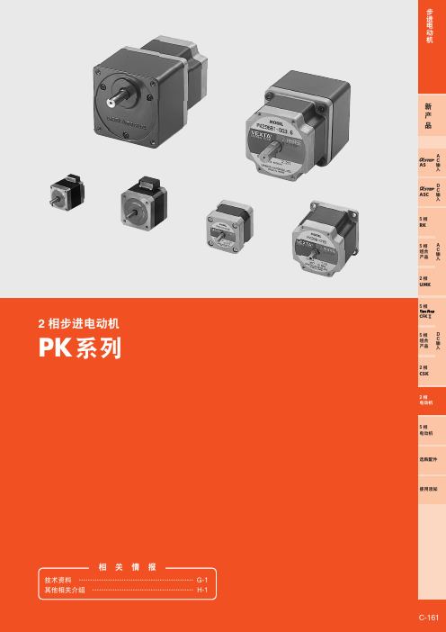
种类 C-165│ 一般规格 C-1812相步进电动机PK 系列C-161相 关 情 报技术资料 ……………………………………………G-1其他相关介绍 ………………………………………H-1步进电动机5相组合产品2相CSK2相电动机5相电动机选购配件使用须知5相CFK ⅡD C 输入5相RK5相组合产品2相UMKA C 输入ASCD C 输入ASA C 输入新 产品C-162ORIENTAL MOTOR GENERAL CA TALOGUE 2005/20062相步进电动机PK 系列2相PK 系列是1转200分割(1.8°/step )的高转矩·低振动的步进电动机。
除了1转200分割的标准机型外,另外还备有1转400分割的高分辨率型以及高转矩·高分辨率的减速机型。
驱动本系列时需另购驱动器。
■特征●产品种类丰富备有标准、标准P 、高分辨率、大惯性、SH 减速机型等机型。
□28mm □35mm □42mm □42mm □50mm □56.4mmC-1635相组合产品2相CSK2相电动机5相电动机选购配件使用须知5相CFK ⅡD C 输入5相RK5相组合产品2相UMKA C 输入ASCD C 输入ASA C 输入新 产品●2相PK 系列产品种类丰富◇标准型是包含转矩、低振动、低噪音等均衡的基本机型。
◇标准P 型新设计的袖珍型与高转矩电动机。
可获得相等于更大型尺寸的电动机转矩,为机器小型化带来贡献。
采用操作性能卓越的连接器连接方式。
标准型PK264-02A0.39N ·m标准P 型PK244PA0.39N ·m机型品名保持转矩◇高分辨率型基本步距角为标准型一半的0.9°。
可将1转做400分割。
提高分辨率·停止精度,达到低振动化。
◇大惯性型加大转子尺寸,提高转矩。
即使驱动惯性负载较大的装置,也比标准机型更能发挥高响应性。
◇SH 减速机型是可以有效的进行减速、提高转矩、提高分辨率、防振等功能的减速机型。
AMF25中文说明书(全)
按钮和LEDs----------------------------------------------------------------------------------50
显示菜单------------------------------------------------------------------------------------51
怎么看测量的数据?--------------------------------------------------------------------------51
包里有什么?-------------------------------------------------------------------------------6
IL-RA15遥控信号器--------------------------------------------------------------------------6
发电机保护------- -------------------------------------------------------------------------37市电故障-----------------------------------------------------------------------------------39
模拟输入-----------------------------------------------------------------------------------29
BFG425W,115;中文规格书,Datasheet资料
MAX. 10 4.5 30 135 120
UNIT V V mA mW fF GHz dB dB
IC = 25 mA; VCE = 2 V; f = 2 GHz; Tamb = 25 C IC = 25 mA; VCE = 2 V; f = 2 GHz; Tamb = 25 C IC = 2 mA; VCE = 2 V; f = 2 GHz; S = opt CAUTION
1. Gmax is the maximum power gain, if K > 1. If K < 1 then Gmax = MSG; see Figs 6, 7 and 8. 2. ZS is optimized for noise; ZL is optimized for gain.
2010 Sep 15
MIN. 10 4.5 1 50
TYP. 80 300 575 95 25 20 17 0.8 1.2 12 22
MAX. 15 120
UNIT V V V nA fF fF fF GHz dB dB dB dB dBm dBm
Fig.6
Maximum stable gain as a function of collector current; typical values.
2010 Sep 15
5
/
NXP Semiconductors
Product specification
15
10 10 5
0 1 10 IC (mA)
102
0 0 10 20 30 IC (mA) 40
VCE = 2 V; f = 2 GHz; Tamb = 25 C.
FTA中文手册

UV处理组与未处理组对照,阴性对照与阳性对照。
GE Healthcare
5
FTA卡的选择与使用方法 如何选择FTA卡和FTA Elute卡?
基因组DNA 如:血液,细胞,组织,植物,细菌,体液等
是否需要溶液形式的DNA?
否
是
您的下游应用是什么?
干血点方法是将采集的血样滴加在特殊的纸介 质上(通常是滤纸),干燥后可以长期保存或经 抽提后分析抽提液中的目标物。FTA卡则是对干 血点技术良好的诠释。
FTA卡作为Whatman的一项专利技术,独创性的 应用于室温下DNA和RNA的采集、运输、纯化和 储存,所有工作均在一张卡上完成。Whatman 已成为这一市场技术的领导者。
您的下游应用是什么?
单次反应:PCR,STR,RFLP,Invader Assay,SNP,WGA
DNA固化形式―FTA!
多次反应:PCR,STR,RFLP,Invader Assay,SNP,WGA;定量PCR等
DNA溶液形式―FTA Elute !
FTA的操作方法
FTA Elute的操作方法
Apply sample
备注:室温保存记录
FTA 指示型 FTA
+ + +
17.5年,并被刷新 8年,并被刷新 4年,并被刷新 4年,并被刷新
7周,并被刷新
FTA Elute 指示型FTA Elute
+ + +
12.1年,并被刷新 3年,并被刷新 3年,并被刷新 N/A
N/A +
A. 血样的室温保存记录 血样保存于FTA卡17年7个月,DNA 扩增后的STR结果
25LC640中文翻译资料

25LC640中文翻译资料山东泰开自动化李凯设备选择表(25AA64025C640)64KSPI总线串口EEPROM:封装类型:方块图特征:低功率COMS工艺-写电流:3mA标准-读电流:500u标准-待机电流:500nA标准8192某8位组织32字节页写周期时间:5mA最大自动同步擦除和写入周期块写入保护-未保护,1/4,1/2,或全部数组内置的写保护-电源开/关数据保护电路-写允许锁存器-写保护管脚连续读高可靠性-耐久度:1M周期(可保证的)-数据保持:大于200年-静电防护:大于4000V8脚PDIP,SOPC,和TSSOP封装温度范围支持;-商业级:(C)0℃至+70℃-工业级:(I)-40℃至+85℃-汽车级:(E)-40℃至+125℃说明:美国微芯科技公司的25AA640/25LC640/25C640(25某某640)是64K 比特电可擦除PROM。
这个存储器的使用通道是简单串行外围接口(SPI)兼容串行总线。
这个总线信号需要时钟输入(SCK)加单独数据在(SI)和数据输出(SO)连线。
进入装置的控制是通过芯片选择(CS)输入。
通信到装置能够暂停通道保持管脚(HOLD)。
虽然装置是暂停,转变在输入将是忽略,除了志片的选择,允许主动服务较高优先级的中断。
1.0电气特性图形1-1:AC测试电路1.1最大等级Vcc.................................7.0V全部输入和输出w.r.t.V...-0.6至Vcc+1.0V储存温度.....................-65℃至150℃引线的焊接温度(10秒).............+300℃静电保护在全部管脚...................4kV注意:强调以上这些列出关于“最大等级”可能引出永久损伤到设备。
这强调的等级仅和设备的功能操作,而且那些或任何其它的条件超出那些声明在说明书的操作表中是未隐含的。
ncep85t25场效应管参数
ncep85t25场效应管参数(原创版)目录1.NCEP85T25 场效应管简介2.NCEP85T25 场效应管参数列表3.参数详解3.1 静态工作点3.2 输入阻抗3.3 输出阻抗3.4 增益3.5 线性度3.6 频率响应3.7 功耗3.8 源极电阻4.NCEP85T25 场效应管应用领域正文CEP85T25 是一种场效应管,它是由 NCE 公司生产的一种半导体元器件。
场效应管(Field Effect Transistor,简称 FET)是一种根据半导体材料的电子运动方式而设计的三极管,具有高输入阻抗、低噪声和低功耗等特点,被广泛应用于各种电子设备中。
CEP85T25 场效应管有许多参数,包括静态工作点、输入阻抗、输出阻抗、增益、线性度、频率响应、功耗和源极电阻等。
这些参数决定了场效应管的性能和适用范围。
静态工作点是指场效应管工作时的偏置电压和电流。
NCEP85T25 的静态工作点通常由制造商给出,用户需要根据实际应用需求进行选择。
输入阻抗是指场效应管的输入端对电路的阻抗。
NCEP85T25 的输入阻抗很高,可以达到 10 的 12 次方欧姆,这使得它在电路中具有很好的抗干扰性能。
输出阻抗是指场效应管的输出端对电路的阻抗。
NCEP85T25 的输出阻抗较低,可以提供较大的电流输出。
增益是指场效应管的电压放大倍数。
NCEP85T25 的增益通常在 10 到1000 倍之间,具体数值取决于其工作状态和电路设计。
线性度是指场效应管的输出电压与输入电压之间的线性关系。
NCEP85T25 的线性度较高,可以提供较为准确的信号放大。
频率响应是指场效应管在不同频率下的性能表现。
NCEP85T25 的频率响应较宽,可以在较宽的频率范围内工作。
功耗是指场效应管在工作时消耗的功率。
NCEP85T25 的功耗较低,可以提供高效的信号放大。
源极电阻是指场效应管的源极电阻值。
NCEP85T25 的源极电阻值通常在几十到几百欧姆之间,需要根据实际应用需求进行选择。
kw25n120中文资料

Preliminary
SKW25N120
Fast S-IGBT in NPT-technology with soft, fast recovery anti-parallel EmCon diode
C
• 40% lower Eoff compared to previous generation • Short circuit withstand time – 10 µs
td(on) tr td(off) tf Eon Eoff Ets
Anti-Parallel Diode Characteristic Diode reverse recovery time
Diode reverse recovery charge Diode peak reverse recovery current Diode peak rate of fall of reverse recovery current during tF
trr tS tF Qrr Irrm dirr/dt
Tj=25°C, VCC=800V,IC=25A, VGE=15/0V, RG=22Ω, Energy losses include “tail” and diode reverse recovery.
Tj=25°C, VR=800V, IF=25A, diF/dt=650A/µs
- parallel switching capability
Type SKW25N120
VCE
IC
1200V 25A
Eoff 2.9mJ
Tj
Package
150°C TO-247AC
Maximum Ratings
Parameter
士兰微 SFR25U20PN 说明书
命名规则
产品规格分类
25A 、200V 超快速恢复二极管
描述
SFR25U20PN 是一款超快恢复二极管器件,采用了先进的硅外延平面工艺制作,在工艺参数和图形结构上都进行了精心的设计,使得该系列产品具有较低的正向压降和超快的反向恢复时间。
精确的外延掺杂控制、先进的平面结终端保护结构以及铂掺杂控制少子寿命保证了该产品具有最佳的综合参数、很高的耐用性和可靠性指标。
该产品可广泛应用于开关电源、不间断电源、直流-直流转换器的输出整流级,同时可作为低压转换和断路电机驱动的续流二极管。
特点
∗ 20ns 的超快恢复时间 ∗ 低的正向压降 ∗ 漏电流小 ∗ 150°C 工作结温
极限参数
封装外形图
声明:
•士兰保留说明书的更改权,恕不另行通知!客户在下单前应获取最新版本资料,并验证相关信息是否完整和最新。
•任何半导体产品特定条件下都有一定的失效或发生故障的可能,买方有责任在使用Silan产品进行系统设计和整机制造时遵守安全标准并采取安全措施,以避免潜在失败风险可能造成人身伤害或财产损失情况的发生!
•产品提升永无止境,我公司将竭诚为客户提供更优秀的产品!。
R5F21245SNFP资料

R8C/24 Group, R8C/25 GroupSINGLE-CHIP 16-BIT CMOS MCU1.OverviewThese MCUs are fabricated using a high-performance silicon gate CMOS process, embedding the R8C/Tiny Series CPU core, and are packaged in a 52-pin molded-plastic LQFP or a 64-pin molded-plastic FLGA. It implements sophisticated instructions for a high level of instruction efficiency. With 1 Mbyte of address space, they are capable of executing instructions at high speed.Furthermore, the R8C/25 Group has on-chip data flash (1 KB x 2 blocks).The difference between the R8C/24 Group and R8C/25 Group is only the presence or absence of data flash. Their peripheral functions are the same.1.1ApplicationsElectronic household appliances, office equipment, audio equipment, consumer products, etc.REJ03B0117-0300Rev.3.00Feb 29, 20081.2Performance OverviewTable 1.1 outlines the Functions and Specifications for R8C/24 Group and Table 1.2 outlines the Functions and Specifications for R8C/25 Group.NOTES:1.I 2C bus is a trademark of Koninklijke Philips Electronics N. V.2.Specify the D version if D version functions are to be used.Table 1.1Functions and Specifications for R8C/24 GroupItem SpecificationCPU Number of fundamental instructions89 instructionsMinimum instruction execution time 50 ns (f(XIN) = 20 MHz, VCC = 3.0 to 5.5 V)100 ns (f(XIN) = 10 MHz, VCC = 2.7 to 5.5 V)200 ns (f(XIN) = 5 MHz, VCC = 2.2 to 5.5 V)Operating mode Single-chip Address space 1 Mbyte Memory capacity Refer to Table 1.3 Product Information for R8C/24 GroupPeripheral Functions Ports I/O ports: 41 pins, Input port: 3 pins LED drive ports I/O ports: 8 pinsTimers Timer RA: 8 bits × 1 channelTimer RB: 8 bits × 1 channel(Each timer equipped with 8-bit prescaler)Timer RD: 16 bits × 2 channels(Input capture and output compare circuits)Timer RE: With real-time clock and compare match functionSerial interfaces 2 channels (UART0, UART1)Clock synchronous serial I/O, UARTClock synchronous serial interface 1 channel I 2C bus Interface (1)Clock synchronous serial I/O with chip selectLIN module Hardware LIN: 1 channel (timer RA, UART0)A/D converter 10-bit A/D converter: 1 circuit, 12 channels Watchdog timer 15 bits × 1 channel (with prescaler)Reset start selectableInterrupts Internal: 11 sources, External: 5 sources, Software: 4sources, Priority levels: 7 levelsClock Clock generation circuits 3 circuits•XIN clock generation circuit (with on-chip feedback resistor)•On-chip oscillator (high speed, low speed)High-speed on-chip oscillator has a frequency adjustment function•XCIN clock generation circuit (32 kHz)Real-time clock (timer RE)Oscillation stop detection function XIN clock oscillation stop detection function Voltage detection circuit On-chip Power-on reset circuit On-chipElectrical Characteristics Supply voltage VCC = 3.0 to 5.5 V (f(XIN) = 20 MHz)VCC = 2.7 to 5.5 V (f(XIN) = 10 MHz)VCC = 2.2 to 5.5 V (f(XIN) = 5 MHz)Current consumption Typ. 10 mA (VCC = 5.0 V, f(XIN) = 20 MHz)Typ. 6 mA (VCC = 3.0 V, f(XIN) = 10 MHz)Typ. 2.0 µA (VCC = 3.0 V, wait mode (f(XCIN) = 32 kHz)Typ. 0.7 µA (VCC = 3.0 V, stop mode)Flash Memory Programming and erasure voltage VCC = 2.7 to 5.5 VProgramming and erasure endurance 100 timesOperating Ambient Temperature -20 to 85°C (N version)-40 to 85°C (D version)(2)-20 to 105°C (Y version)(3)Package 52-pin molded-plastic LQFP64-pin molded-plastic FLGATable 1.2Functions and Specifications for R8C/25 GroupNOTES:1.I 2C bus is a trademark of Koninklijke Philips Electronics N. V.2.Specify the D version if D version functions are to be used.Item SpecificationCPU Number of fundamental instructions89 instructionsMinimum instruction execution time 50 ns (f(XIN) = 20 MHz, VCC = 3.0 to 5.5 V)100 ns (f(XIN) = 10 MHz, VCC = 2.7 to 5.5 V)200 ns (f(XIN) = 5 MHz, VCC = 2.2 to 5.5 V)Operating mode Single-chip Address space 1 Mbyte Memory capacity Refer to Table 1.4 Product Information for R8C/25 GroupPeripheral Functions Ports I/O ports: 41 pins, Input port: 3 pins LED drive ports I/O ports: 8 pinsTimers Timer RA: 8 bits × 1 channelTimer RB: 8 bits × 1 channel(Each timer equipped with 8-bit prescaler)Timer RD: 16 bits × 2 channels(Input capture and output compare circuits)Timer RE: With real-time clock and compare match functionSerial interface 2 channels (UART0, UART1)Clock synchronous serial I/O, UARTClock synchronous serial interface 1 channel I 2C bus Interface (1)Clock synchronous serial I/O with chip selectLIN module Hardware LIN: 1 channel (timer RA, UART0)A/D converter 10-bit A/D converter: 1 circuit, 12 channels Watchdog timer 15 bits × 1 channel (with prescaler)Reset start selectableInterrupts Internal: 11 sources, External: 5 sources, Software: 4sources, Priority levels: 7 levelsClock Clock generation circuits 3 circuits•XIN clock generation circuit (with on-chip feedbackresistor)•On-chip oscillator (high speed, low speed)High-speed on-chip oscillator has a frequency adjustment function•XCIN clock generation circuit (32 kHz)Real-time clock (timer RE)Oscillation stop detection function XIN clock oscillation stop detection function Voltage detection circuit On-chip Power-on reset circuit On-chipElectrical Characteristics Supply voltage VCC = 3.0 to 5.5 V (f(XIN) = 20 MHz)VCC = 2.7 to 5.5 V (f(XIN) = 10 MHz)VCC = 2.2 to 5.5 V (f(XIN) = 5 MHz)Current consumption Typ. 10 mA (VCC = 5.0 V, f(XIN) = 20 MHz)Typ. 6 mA (VCC = 3.0 V, f(XIN) = 10 MHz)Typ. 2.0 µA (VCC = 3.0 V, wait mode (f(XCIN) = 32 kHz)Typ. 0.7 µA (VCC = 3.0 V, stop mode)Flash memory Programming and erasure voltage VCC = 2.7 to 5.5 VProgramming and erasure endurance 1,0000 times (data flash)1,000 times (program ROM)Operating Ambient Temperature -20 to 85°C (N version)-40 to 85°C (D version)(2)-20 to 105°C (Y version)(3)Package 52-pin molded-plastic LQFP64-pin molded-plastic FLGA1.3Block DiagramFigure 1.1 shows a Block Diagram.1.4Product InformationTable 1.3 lists the Product Information for R8C/24 Group and Table 1.4 lists the Product Information for R8C/25Group.NOTE:1.The user ROM is programmed before shipment.Table 1.3Product Information for R8C/24 GroupCurrent of Feb. 2008 Type No.ROM Capacity RAM Capacity Package Type Remarks R5F21244SNFP 16 Kbytes 1 Kbyte PLQP0052JA-A N version Blank productR5F21245SNFP 24 Kbytes 2 Kbytes PLQP0052JA-A R5F21246SNFP 32 Kbytes 2 Kbytes PLQP0052JA-A R5F21247SNFP 48 Kbytes 2.5 Kbytes PLQP0052JA-A R5F21248SNFP 64 Kbytes 3 Kbytes PLQP0052JA-A R5F21244SNLG 16 Kbytes 1 Kbyte PTLG0064JA-A R5F21246SNLG 32 Kbytes 2 Kbytes PTLG0064JA-A R5F21244SDFP 16 Kbytes 1 Kbyte PLQP0052JA-A D version Blank productR5F21245SDFP 24 Kbytes 2 Kbytes PLQP0052JA-A R5F21246SDFP 32 Kbytes 2 Kbytes PLQP0052JA-A R5F21247SDFP 48 Kbytes 2.5 Kbytes PLQP0052JA-A R5F21248SDFP64 Kbytes 3 Kbytes PLQP0052JA-A R5F21244SNXXXFP 16 Kbytes 1 Kbyte PLQP0052JA-A N version Factoryprogramming product (1)R5F21245SNXXXFP 24 Kbytes 2 Kbytes PLQP0052JA-A R5F21246SNXXXFP 32 Kbytes 2 Kbytes PLQP0052JA-A R5F21247SNXXXFP 48 Kbytes 2.5 Kbytes PLQP0052JA-A R5F21248SNXXXFP 64 Kbytes 3 Kbytes PLQP0052JA-A R5F21244SNXXXLG 16 Kbytes 1 Kbyte PTLG0064JA-A R5F21246SNXXXLG 32 Kbytes 2 Kbytes PTLG0064JA-A R5F21244SDXXXFP 16 Kbytes 1 Kbyte PLQP0052JA-A D version Factoryprogramming product (1)R5F21245SDXXXFP 24 Kbytes 2 Kbytes PLQP0052JA-A R5F21246SDXXXFP 32 Kbytes 2 Kbytes PLQP0052JA-A R5F21247SDXXXFP 48 Kbytes 2.5 Kbytes PLQP0052JA-A R5F21248SDXXXFP64 Kbytes3 KbytesPLQP0052JA-ANOTE:1.The user ROM is programmed before shipment.Table 1.4Product Information for R8C/25 GroupCurrent of Feb. 2008Type No.ROM CapacityRAMCapacity Package Type Remarks Program ROM Data flash R5F21254SNFP 16 Kbytes 1 Kbyte × 2 1 Kbyte PLQP0052JA-A N version Blank productR5F21255SNFP 24 Kbytes 1 Kbyte × 2 2 Kbytes PLQP0052JA-A R5F21256SNFP 32 Kbytes 1 Kbyte × 2 2 Kbytes PLQP0052JA-A R5F21257SNFP 48 Kbytes 1 Kbyte × 2 2.5 Kbytes PLQP0052JA-A R5F21258SNFP 64 Kbytes 1 Kbyte × 2 3 Kbytes PLQP0052JA-A R5F21254SNLG 16 Kbytes 1 Kbyte × 2 1 Kbyte PTLG0064JA-A R5F21256SNLG 32 Kbytes 1 Kbyte × 2 2 Kbytes PTLG0064JA-A R5F21254SDFP 16 Kbytes 1 Kbyte × 2 1 Kbyte PLQP0052JA-A D version Blank productR5F21255SDFP 24 Kbytes 1 Kbyte × 2 2 Kbytes PLQP0052JA-A R5F21256SDFP 32 Kbytes 1 Kbyte × 2 2 Kbytes PLQP0052JA-A R5F21257SDFP 48 Kbytes 1 Kbyte × 2 2.5 Kbytes PLQP0052JA-A R5F21258SDFP64 Kbytes 1 Kbyte × 2 3 Kbytes PLQP0052JA-A R5F21254SNXXXFP 16 Kbytes 1 Kbyte × 2 1 Kbyte PLQP0052JA-A N version Factoryprogramming product (1)R5F21255SNXXXFP 24 Kbytes 1 Kbyte × 2 2 Kbytes PLQP0052JA-A R5F21256SNXXXFP 32 Kbytes 1 Kbyte × 2 2 Kbytes PLQP0052JA-A R5F21257SNXXXFP 48 Kbytes 1 Kbyte × 2 2.5 Kbytes PLQP0052JA-A R5F21258SNXXXFP 64 Kbytes 1 Kbyte × 2 3 Kbytes PLQP0052JA-A R5F21254SNXXXLG 16 Kbytes 1 Kbyte × 2 1 Kbyte PTLG0064JA-A R5F21256SNXXXLG 32 Kbytes 1 Kbyte × 2 2 Kbytes PTLG0064JA-A R5F21254SDXXXFP 16 Kbytes 1 Kbyte × 2 1 Kbyte PLQP0052JA-A D version Factoryprogramming product (1)R5F21255SDXXXFP 24 Kbytes 1 Kbyte × 2 2 Kbytes PLQP0052JA-A R5F21256SDXXXFP 32 Kbytes 1 Kbyte × 2 2 Kbytes PLQP0052JA-A R5F21257SDXXXFP 48 Kbytes 1 Kbyte × 2 2.5 Kbytes PLQP0052JA-A R5F21258SDXXXFP64 Kbytes 1 Kbyte × 23 KbytesPLQP0052JA-A1.5Pin AssignmentsFigure 1.4 shows PLQP0052JA-A Package Pin Assignments (Top View). Figure 1.5 shows PTLG0064JA-A Package Pin Assignments.1.6Pin FunctionsTable 1.5 lists Pin Functions.I: InputO: OutputI/O: Input and outputTable 1.5Pin FunctionsTypeSymbolI/O TypeDescriptionPower supply input VCC, VSS I Apply 2.2 V to 5.5 V to the VCC pin. Apply 0 V to the VSS pin.Analog power supply input AVCC, AVSS I Power supply for the A/D converter.Connect a capacitor between AVCC and AVSS.Reset input RESET I Input “L” on this pin resets the MCU.MODE MODE I Connect this pin to VCC via a resistor.XIN clock input XIN I These pins are provided for XIN clock generation circuit I/O.Connect a ceramic resonator or a crystal oscillator between the XIN and XOUT pins. To use an external clock, input it to the XIN pin and leave the XOUT pin open.XIN clock output XOUT O XCIN clock input XCIN I These pins are provided for XCIN clock generation circuit I/O.Connect a crystal oscillator between the XCIN and XCOUT pins. To use an external clock, input it to the XCIN pin and leave the XCOUT pin open.XCIN clock output XCOUT O INT interrupt input INT0 to INT3I INT interrupt input pins.INT0 is timer RD input pin. INT1 is timer RA input pin.Key input interrupt KI0 to KI3I Key input interrupt input pins Timer RA TRAIO I/O Timer RA I/O pin TRAO O Timer RA output pin Timer RB TRBOO Timer RB output pin Timer RDTRDIOA0, TRDIOA1,TRDIOB0, TRDIOB1,TRDIOC0, TRDIOC1,TRDIOD0, TRDIOD1I/OTimer RD I/O portsTRDCLK I External clock input pin Timer RE TREO O Divided clock output pin Serial interfaceCLK0, CLK1I/O Transfer clock I/O pin RXD0, RXD1I Serial data input pins TXD0, TXD1O Serial data output pins I 2C bus interfaceSCL I/O Clock I/O pin SDAI/O Data I/O pin Clock synchronous serial I/O with chip selectSSI I/O Data I/O pinSCS I/O Chip-select signal I/O pin SSCKI/O Clock I/O pin SSOI/O Data I/O pinReference voltage input VREF I Reference voltage input pin to A/D converter A/D converter AN0 to AN11I Analog input pins to A/D converterI/O portP0_0 to P0_7, P1_0 to P1_7, P2_0 to P2_7, P3_0, P3_1,P3_3 to P3_5, P3_7, P4_3 to P4_5, P6_0 to P6_7I/OCMOS I/O ports. Each port has an I/O select direction register, allowing each pin in the port to be directed for input or output individually.Any port set to input can be set to use a pull-up resistor or not by a program.P2_0 to P2_7 also function as LED drive ports.Input port P4_2, P4_6, P4_7IInput-only portsNOTE:1.Can be assigned to the pin in parentheses by a program.Table 1.6Pin Name Information by Pin NumberPinNumber Control PinPortI/O Pin Functions for of Peripheral ModulesInterruptTimerSerial Interface ClockSynchronous Serial I/O with Chip Select I 2C busInterfaceA/D Converter2P3_5SSCK SCL 3P3_3SSI4P3_4SCSSDA5MODE 6XCIN P4_37XCOUT P4_48RESET 9XOUT P4_710VSS/AVSS11XIN P4_612VCC/AVCC13P2_7TRDIOD114P2_6TRDIOC115P2_5TRDIOB116P2_4TRDIOA117P2_3TRDIOD018P2_2TRDIOC019P2_1TRDIOB020P2_0TRDIOA0/TRDCLK21P1_7INT1TRAIO22P1_6CLK023P1_5(INT1)(1)(TRAIO)(1)RXD024P1_4TXD025P1_3KI3AN1127P4_5INT0INT028P6_6INT2TXD129P6_7INT3RXD130P1_2KI2AN1031P1_1KI1AN932P1_0KI0AN833P3_1TRBO 34P3_0TRAO35P6_5CLK136P6_437P6_338P0_7AN041P0_6AN142P0_5AN243P0_4AN344VREFP4_245P6_0TREO46P6_247P6_148P0_3AN449P0_2AN550P0_1AN651P0_0AN752P3_7SSO2.Central Processing Unit (CPU)Figure 2.1 shows the CPU Registers. The CPU contains 13 registers. R0, R1, R2, R3, A0, A1, and FB configure a register bank. There are two sets of register bank.2.1Data Registers (R0, R1, R2, and R3)R0 is a 16-bit register for transfer, arithmetic, and logic operations. The same applies to R1 to R3. R0 can be split into high-order bits (R0H) and low-order bits (R0L) to be used separately as 8-bit data registers. R1H and R1L are analogous to R0H and R0L. R2 can be combined with R0 and used as a 32-bit data register (R2R0). R3R1 is analogous to R2R0.2.2Address Registers (A0 and A1)A0 is a 16-bit register for address register indirect addressing and address register relative addressing. It is also used for transfer, arithmetic, and logic operations. A1 is analogous to A0. A1 can be combined with A0 and as a 32-bit address register (A1A0).2.3Frame Base Register (FB)FB is a 16-bit register for FB relative addressing.2.4Interrupt Table Register (INTB)INTB is a 20-bit register that indicates the start address of an interrupt vector table.2.5Program Counter (PC)PC is 20 bits wide and indicates the address of the next instruction to be executed.2.6User Stack Pointer (USP) and Interrupt Stack Pointer (ISP)The stack pointers (SP), USP, and ISP, are each 16 bits wide. The U flag of FLG is used to switch betweenUSP and ISP.2.7Static Base Register (SB)SB is a 16-bit register for SB relative addressing.2.8Flag Register (FLG)FLG is an 11-bit register indicating the CPU state.2.8.1Carry Flag (C)The C flag retains carry, borrow, or shift-out bits that have been generated by the arithmetic and logic unit.2.8.2Debug Flag (D)The D flag is for debugging only. Set it to 0.2.8.3Zero Flag (Z)The Z flag is set to 1 when an arithmetic operation results in 0; otherwise to 0.2.8.4Sign Flag (S)The S flag is set to 1 when an arithmetic operation results in a negative value; otherwise to 0.2.8.5Register Bank Select Flag (B)Register bank 0 is selected when the B flag is 0. Register bank 1 is selected when this flag is set to 1.2.8.6Overflow Flag (O)The O flag is set to 1 when an operation results in an overflow; otherwise to 0.2.8.7Interrupt Enable Flag (I)The I flag enables maskable interrupts.Interrupt are disabled when the I flag is set to 0, and are enabled when the I flag is set to 1. The I flag is set to 0 when an interrupt request is acknowledged.2.8.8Stack Pointer Select Flag (U)ISP is selected when the U flag is set to 0; USP is selected when the U flag is set to 1.The U flag is set to 0 when a hardware interrupt request is acknowledged or the INT instruction of software interrupt numbers 0 to 31 is executed.2.8.9Processor Interrupt Priority Level (IPL)IPL is 3 bits wide and assigns processor interrupt priority levels from level 0 to level 7.If a requested interrupt has higher priority than IPL, the interrupt is enabled.2.8.10Reserved BitIf necessary, set to 0. When read, the content is undefined.3.Memory3.1R8C/24 GroupFigure 3.1 is a Memory Map of R8C/24 Group. The R8C/24 group has 1 Mbyte of address space from addresses 00000h to FFFFFh.The internal ROM is allocated lower addresses, beginning with address 0FFFFh. For example, a 48-Kbyte internal ROM area is allocated addresses 04000h to 0FFFFh.The fixed interrupt vector table is allocated addresses 0FFDCh to 0FFFFh. They store the starting address of each interrupt routine.The internal RAM is allocated higher addresses, beginning with address 00400h. For example, a 2-Kbyte internal RAM area is allocated addresses 00400h to 00BFFh. The internal RAM is used not only for storing data but also for calling subroutines and as stacks when interrupt requests are acknowledged.Special function registers (SFRs) are allocated addresses 00000h to 002FFh. The peripheral function control registers are allocated here. All addresses within the SFR, which have nothing allocated are reserved for future use and cannot be accessed by users.3.2R8C/25 GroupFigure 3.2 is a Memory Map of R8C/25 Group. The R8C/25 group has 1 Mbyte of address space from addresses 00000h to FFFFFh.The internal ROM (program ROM) is allocated lower addresses, beginning with address 0FFFFh. For example, a 48-Kbyte internal ROM area is allocated addresses 04000h to 0FFFFh.The fixed interrupt vector table is allocated addresses 0FFDCh to 0FFFFh. They store the starting address of each interrupt routine.The internal ROM (data flash) is allocated addresses 02400h to 02BFFh.The internal RAM area is allocated higher addresses, beginning with address 00400h. For example, a 2-Kbyte internal RAM is allocated addresses 00400h to 00BFFh. The internal RAM is used not only for storing data but also for calling subroutines and as stacks when interrupt requests are acknowledged.Special function registers (SFRs) are allocated addresses 00000h to 002FFh. The peripheral function control registers are allocated here. All addresses within the SFR, which have nothing allocated are reserved for future use and cannot be accessed by users.4.Special Function Registers (SFRs)An SFR (special function register) is a control register for a peripheral function. Tables 4.1 to 4.7 list the special function registers.Table 4.1SFR Information (1)(1)X: Undefined NOTES:1.The blank regions are reserved. Do not access locations in these regions.2.Software reset, watchdog timer reset, and voltage monitor 1 reset or voltage monitor 2 reset do not affect this register.3.The LVD0ON bit in the OFS register is set to 1 and hardware reset.4.Power-on reset, voltage monitor 0 reset or the LVD0ON bit in the OFS register is set to 0, and hardware reset.5.Software reset, watchdog timer reset, and voltage monitor 1 reset or voltage monitor 2 reset do not affect b2 and b3.6.The CSPROINI bit in the OFS register is set to 0.Address RegisterSymbolAfter reset0000h 0001h 0002h 0003h 0004h Processor Mode Register 0PM000h 0005h Processor Mode Register 1PM100h0006h System Clock Control Register 0CM001101000b 0007h System Clock Control Register 1CM100100000b0008h 0009h 000Ah Protect RegisterPRCR 00h 000Bh 000Ch Oscillation Stop Detection Register OCD 00000100b 000Dh Watchdog Timer Reset Register WDTR XXh 000Eh Watchdog Timer Start Register WDTS XXh000Fh Watchdog Timer Control Register WDC 00X11111b 0010h Address Match Interrupt Register 0RMAD000h 0011h 00h 0012h 00h 0013h Address Match Interrupt Enable Register AIER 00h 0014h Address Match Interrupt Register 1RMAD100h 0015h 00h 0016h 00h0017h 0018h 0019h 001Ah 001Bh 001Ch Count Source Protection Mode Register CSPR00h10000000b (6)001Dh 001Eh 001Fh 0020h 0021h 0022h 0023h High-Speed On-Chip Oscillator Control Register 0FRA000h0024h High-Speed On-Chip Oscillator Control Register 1FRA1When shipping 0025h High-Speed On-Chip Oscillator Control Register 2FRA200h0026h 0027h 0028h Clock Prescaler Reset FlagCPSRF 00h0029h High-Speed On-Chip Oscillator Control Register 4FRA4When shipping 002Ah 002Bh High-Speed On-Chip Oscillator Control Register 6FRA6When shipping 002Ch High-Speed On-Chip Oscillator Control Register 7FRA7When shipping0030h 0031h Voltage Detection Register 1(2)VCA100001000b 0032h Voltage Detection Register 2(2)VCA200h (3)00100000b (4)0033h 0034h 0035h 0036h Voltage Monitor 1 Circuit Control Register (5)VW1C 00001000b 0037h Voltage Monitor 2 Circuit Control Register (5)VW2C 00h0038h Voltage Monitor 0 Circuit Control Register (2)VW0C0000X000b (3)0100X001b (4)0039h 003Ah003Eh 003FhTable 4.2SFR Information (2)(1)Address Register Symbol After reset 0040h0041h0042h0043h0044h0045h0046h0047h0048h Timer RD0 Interrupt Control Register TRD0IC XXXXX000b 0049h Timer RD1 Interrupt Control Register TRD1IC XXXXX000b 004Ah Timer RE Interrupt Control Register TREIC XXXXX000b 004Bh004Ch004Dh Key Input Interrupt Control Register KUPIC XXXXX000b 004Eh A/D Conversion Interrupt Control Register ADIC XXXXX000b 004Fh SSU/IIC Interrupt Control Register(2)SSUIC / IICIC XXXXX000b 0050h0051h UART0 Transmit Interrupt Control Register S0TIC XXXXX000b 0052h UART0 Receive Interrupt Control Register S0RIC XXXXX000b 0053h UART1 Transmit Interrupt Control Register S1TIC XXXXX000b 0054h UART1 Receive Interrupt Control Register S1RIC XXXXX000b 0055h INT2 Interrupt Control Register INT2IC XX00X000b 0056h Timer RA Interrupt Control Register TRAIC XXXXX000b 0057h0058h Timer RB Interrupt Control Register TRBIC XXXXX000b 0059h INT1 Interrupt Control Register INT1IC XX00X000b 005Ah INT3 Interrupt Control Register INT3IC XX00X000b 005Bh005Ch005Dh INT0 Interrupt Control Register INT0IC XX00X000b 005Eh005Fh0060h0061h0062h0063h0064h0065h0066h0067h0068h0069h006Ah006Bh006Ch006Dh006Eh006Fh0070h0071h0072h0073h0074h0075h0076h0077h0078h0079h007Ah007Bh007Ch007Dh007Eh007FhX: UndefinedNOTES:1.The blank regions are reserved. Do not access locations in these regions.2.Selected by the IICSEL bit in the PMR register.Table 4.3SFR Information (3)(1)Address Register Symbol After reset 0080h0081h0082h0083h0084h0085h0086h0087h0088h0089h008Ah008Bh008Ch008Dh008Eh008Fh0090h0091h0092h0093h0094h0095h0096h0097h0098h0099h009Ah009Bh009Ch009Dh009Eh009Fh00A0h UART0 Transmit/Receive Mode Register U0MR00h00A1h UART0 Bit Rate Register U0BRG XXh00A2h UART0 Transmit Buffer Register U0TB XXh00A3h XXh00A4h UART0 Transmit/Receive Control Register 0U0C000001000b 00A5h UART0 Transmit/Receive Control Register 1U0C100000010b 00A6h UART0 Receive Buffer Register U0RB XXh00A7h XXh00A8h UART1 Transmit/Receive Mode Register U1MR00h00A9h UART1 Bit Rate Register U1BRG XXh00AAh UART1 Transmit Buffer Register U1TB XXh00ABh XXh00ACh UART1 Transmit/Receive Control Register 0U1C000001000b 00ADh UART1 Transmit/Receive Control Register 1U1C100000010b 00AEh UART1 Receive Buffer Register U1RB XXh00AFh XXh00B0h00B1h00B2h00B3h00B4h00B5h00B6h00B7h00B8h SS Control Register H / IIC bus Control Register 1(2)SSCRH / ICCR100h00B9h SS Control Register L / IIC bus Control Register 2(2)SSCRL / ICCR201111101b 00BAh SS Mode Register / IIC bus Mode Register(2)SSMR / ICMR00011000b 00BBh SS Enable Register / IIC bus Interrupt Enable Register(2)SSER / ICIER00h00BCh SS Status Register / IIC bus Status Register(2)SSSR / ICSR00h / 0000X000b 00BDh SS Mode Register 2 / Slave Address Register(2)SSMR2 / SAR00h00BEh SS Transmit Data Register / IIC bus Transmit Data Register(2)SSTDR / ICDRT FFh00BFh SS Receive Data Register / IIC bus Receive Data Register(2)SSRDR / ICDRR FFhX: UndefinedNOTES:1.The blank regions are reserved. Do not access locations in these regions.2.Selected by the IICSEL bit in the PMR register.Table 4.4SFR Information (4)(1)Address Register Symbol After reset 00C0h A/D Register AD XXh00C1h XXh00C2h00C3h00C4h00C5h00C6h00C7h00C8h00C9h00CAh00CBh00CCh00CDh00CEh00CFh00D0h00D1h00D2h00D3h00D4h A/D Control Register 2ADCON200h00D5h00D6h A/D Control Register 0ADCON000h00D7h A/D Control Register 1ADCON100h00D8h00D9h00DAh00DBh00DCh00DDh00DEh00DFh00E0h Port P0 Register P0XXh00E1h Port P1 Register P1XXh00E2h Port P0 Direction Register PD000h00E3h Port P1 Direction Register PD100h00E4h Port P2 Register P2XXh00E5h Port P3 Register P3XXh00E6h Port P2 Direction Register PD200h00E7h Port P3 Direction Register PD300h00E8h Port P4 Register P4XXh00E9h00EAh Port P4 Direction Register PD400h00EBh00ECh Port P6 Register P6XXh00EDh00EEh Port P6 Direction Register PD600h00EFh00F0h00F1h00F2h00F3h00F4h Port P2 Drive Capacity Control Register P2DRR00h00F5h UART1 Function Select Register U1SR XXh00F6h00F7h00F8h Port Mode Register PMR00h00F9h External Input Enable Register INTEN00h00FAh INT Input Filter Select Register INTF00h00FBh Key Input Enable Register KIEN00h00FCh Pull-Up Control Register 0PUR000h00FDh Pull-Up Control Register 1PUR1XX00XX00b 00FEh00FFhX: UndefinedNOTE:1.The blank regions are reserved. Do not access locations in these regions.Table 4.5SFR Information (5)(1)Address Register Symbol After reset 0100h Timer RA Control Register TRACR00h0101h Timer RA I/O Control Register TRAIOC00h0102h Timer RA Mode Register TRAMR00h0103h Timer RA Prescaler Register TRAPRE FFh0104h Timer RA Register TRA FFh0105h0106h LIN Control Register LINCR00h0107h LIN Status Register LINST00h0108h Timer RB Control Register TRBCR00h0109h Timer RB One-Shot Control Register TRBOCR00h010Ah Timer RB I/O Control Register TRBIOC00h010Bh Timer RB Mode Register TRBMR00h010Ch Timer RB Prescaler Register TRBPRE FFh010Dh Timer RB Secondary Register TRBSC FFh010Eh Timer RB Primary Register TRBPR FFh010Fh0110h0111h0112h0113h0114h0115h0116h0117h0118h Timer RE Second Data Register / Counter Data Register TRESEC00h0119h Timer RE Minute Data Register / Compare Data Register TREMIN00h011Ah Timer RE Hour Data Register TREHR00h011Bh Timer RE Day of Week Data Register TREWK00h011Ch Timer RE Control Register 1TRECR100h011Dh Timer RE Control Register 2TRECR200h011Eh Timer RE Count Source Select Register TRECSR00001000b 011Fh0120h0121h0122h0123h0124h0125h0126h0127h0128h0129h012Ah012Bh012Ch012Dh012Eh012Fh0130h0131h0132h0133h0134h0135h0136h0137h Timer RD Start Register TRDSTR11111100b 0138h Timer RD Mode Register TRDMR00001110b 0139h Timer RD PWM Mode Register TRDPMR10001000b 013Ah Timer RD Function Control Register TRDFCR10000000b 013Bh Timer RD Output Master Enable Register 1TRDOER1FFh013Ch Timer RD Output Master Enable Register 2TRDOER201111111b 013Dh Timer RD Output Control Register TRDOCR00h013Eh Timer RD Digital Filter Function Select Register 0TRDDF000h013Fh Timer RD Digital Filter Function Select Register 1TRDDF100hX: UndefinedNOTE:1.The blank regions are reserved. Do not access locations in these regions.。
TMG25CQ60F资料
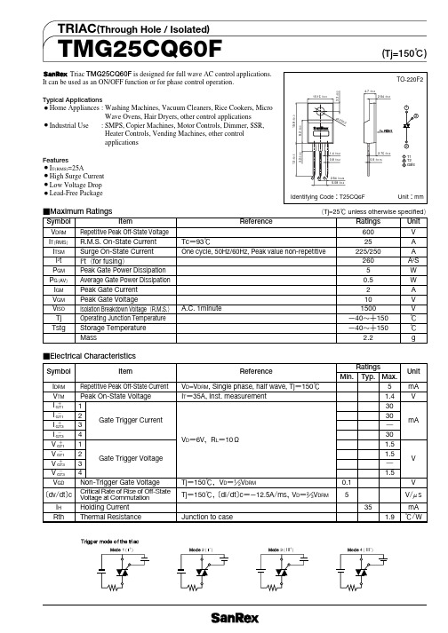
IT(RMS)=25A High Surge Current Low Voltage Drop Lead-Free Package
Identifying Code T25CQ6F
Unit mm
Maximum Ratings
Symbol VDRM IT RMS ITSM I2t PGM PG AV IGM VGM VISO Tj Tstg Item Repetitive Peak Off-State Voltage R.M.S. On-State Current Surge On-State Current I2t for fusing Peak Gate Power Dissipation Average Gate Power Dissipation Peak Gate Current Peak Gate Voltage Isolation Breakdown Voltage R.M.S. Operating Junction Temperature Storage Temperature Mass Reference
Unit V A A A2S W W A V V
g
Electrical Characteristics
Symbol IDRM VTM I GT1 I GT1 I GT3 I GT3 V GT1 V GT1 V GT3 V GT3 VGD dv/dt c IH Rth Item Repetitive Peak Off-State Current Peak On-State Voltage 1 2 Gate Trigger Current 3 4 1 2 Gate Trigger Voltage 3 4 Non-Trigger Gate Voltage
Eaton Moeller PKN4-25 1N C 03-G-MW 型号的一份产品说明书
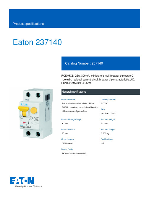
Eaton 237140RCD/MCB, 25A, 300mA, miniature circuit-breaker trip curve C, 1pole+N, residual current circuit-breaker trip characteristic: AC. PKN4-25/1N/C/03-G-MWGeneral specificationsEaton Moeller series xPole - PKN4 RCBO - residual-current circuit breaker with overcurrent protection237140401508237140180 mm 73 mm 35 mm 0.203 kg CE Marked CEPKN4-25/1N/C/03-G-MWProduct NameCatalog Number EANProduct Length/Depth Product Height Product Width Product Weight Compliances Certifications Model CodeSwitchgear for residential and commercial applications PKN4Combined RCD/MCB devicesSingle-pole + N12CC25 A0.3 AType G (ÖVE E 8601), AC current sensitiveRCBO AC230 V440 V4 kVSurge-proof, 3 kA 50 HzOther4.5 kA0 kA4.5 kA0 kA4.5 kA4.5 kA3 kAShort-time delayed Short time-delayed IIIApplicationProduct rangeBasic functionNumber of polesNumber of poles (protected) Number of poles (total) Tripping characteristic Release characteristic Rated currentFault current rating Sensitivity typeType Voltage typeVoltage ratingRated insulation voltage (Ui)Rated impulse withstand voltage (Uimp)Impulse withstand currentFrequency ratingLeakage current typeRated switching capacityRated switching capacity (IEC/EN 60947-2) Rated switching capacity (IEC/EN 61009)Rated short-circuit breaking capacity (EN 60947-2) Rated short-circuit breaking capacity (EN 61009) Rated short-circuit breaking capacity (EN 61009-1) Surge current capacityDisconnection characteristicTrippingOvervoltage categoryPollution degree2269.5 mmIP201 mm²25 mm²1 mm²25 mm²25 A 0 W 4.8 W 0 W 0 W Meets the product standard's requirements.Meets the product standard's requirements.Meets the product standard's requirements.Meets the product standard's requirements.Meets the product standard's requirements.Does not apply, since the entire switchgear needs to be evaluated.Does not apply, since the entire switchgear needs to be evaluated.Meets the product standard's requirements.Width in number of modular spacingsBuilt-in depthDegree of protectionConnectable conductor cross section (solid-core) - minConnectable conductor cross section (solid-core) - maxConnectable conductor cross section (multi-wired) - minConnectable conductor cross section (multi-wired) - maxRated operational current for specified heat dissipation (In) Heat dissipation per pole, current-dependentEquipment heat dissipation, current-dependentStatic heat dissipation, non-current-dependentHeat dissipation capacity 10.2.2 Corrosion resistance10.2.3.1 Verification of thermal stability of enclosures10.2.3.2 Verification of resistance of insulating materials to normal heat10.2.3.3 Resist. of insul. mat. to abnormal heat/fire by internal elect. effects10.2.4 Resistance to ultra-violet (UV) radiation10.2.5 Lifting10.2.6 Mechanical impact10.2.7 InscriptionsDoes not apply, since the entire switchgear needs to be evaluated.Meets the product standard's requirements.Does not apply, since the entire switchgear needs to be evaluated.Does not apply, since the entire switchgear needs to be evaluated.Is the panel builder's responsibility.Is the panel builder's responsibility.Is the panel builder's responsibility.Is the panel builder's responsibility.Is the panel builder's responsibility.The panel builder is responsible for the temperature rise calculation. Eaton will provide heat dissipation data for the devices.Is the panel builder's responsibility. The specifications for the switchgear must be observed.Is the panel builder's responsibility. The specifications for the switchgear must be observed.The device meets the requirements, provided the information in the instruction leaflet (IL) is observed.3Anti-nuisance tripping version Concurrently switching N-neutral10.3 Degree of protection of assemblies10.4 Clearances and creepage distances10.5 Protection against electric shock10.6 Incorporation of switching devices and components 10.7 Internal electrical circuits and connections10.8 Connections for external conductors10.9.2 Power-frequency electric strength10.9.3 Impulse withstand voltage10.9.4 Testing of enclosures made of insulating material 10.10 Temperature rise10.11 Short-circuit rating10.12 Electromagnetic compatibility10.13 Mechanical function Current limiting class FeaturesEaton Corporation plc Eaton House30 Pembroke Road Dublin 4, Ireland © 2023 Eaton. All rights reserved. Eaton is a registered trademark.All other trademarks areproperty of their respectiveowners./socialmedia。
- 1、下载文档前请自行甄别文档内容的完整性,平台不提供额外的编辑、内容补充、找答案等附加服务。
- 2、"仅部分预览"的文档,不可在线预览部分如存在完整性等问题,可反馈申请退款(可完整预览的文档不适用该条件!)。
- 3、如文档侵犯您的权益,请联系客服反馈,我们会尽快为您处理(人工客服工作时间:9:00-18:30)。
Ratings 10 10 1.55 50/3 0.25 10 500 50 100 0.78
Unit mA mA V mA/V V s V/ s mA mA /W
mark Thyristor and Diode part. No mark
SanRex 50 Seaview Blvd. Port Washington, NY 11050-4618 PH.(516)625-1313 FAX(516)625-8845 E-mail: semi@
元器件交易网
THYRISTOR MODULE
PK(PD,PE,KK)25F
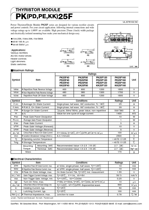
UL:E76102 M Power Thyristor/Diode Module PK25F series are designed for various rectifier circuits and power controls. For your circuit application. following internal connections and wide voltage ratings up to 1,600V are available. High precision 25mm (1inch) width package and electrically isolated mounting base make your mechanical design easy. IT(AV) 25A, IT(RMS) 39A, ITSM 580A di/dt 100 A/ s dv/dt 500V/ s Applications Various rectifiers AC/DC motor drives Heater controls Light dimmers Static switches25 12.5 2K1 G1 K2 G2
M5X10
2.8 #110TAB
PK
PE
31max 19.5
80 0.2
PD
KK
Maximum Ratings
Ratings Symbol Item PK25F40 PD25F40 PE25F40 KK25F40 400 480 400 PK25F80 PD25F80 PE25F80 KK25F80 800 960 800 PK25F120 PD25F120 PE25F120 KK25F120 1200 1300 1200 PK25F160 PD25F160 PE25F160 KK25F160 1600 1700 1600 Ratings 25 39 530/580 1400 10 1 3 10 5 100 2500 40 125 40 125 2.7 28 2.7 28 170 Unit
Thyristor part
Conditions at VDRM, single phase, half wave, Tj 125 at VDRM, single phase, half wave, Tj 125 On-State Current 75A, Tj 25 Inst. measurement Tj 25 IT 1A VD 6V Tj 125 VD 1 2VDRM T 25A IG 100mA Tj 25 I VD 1 2VDRM dIG/dt 1A/ s 2 VDRM, Exponential wave. Tj 125 , VD 3 Tj 25 Tj 25 Junction to case
VRRM VRSM VDRM Symbol IT AV IT RMS ITSM I2t PGM PG AV IFGM VFGM VRGM di dt VISO Tj Tstg
6.5 29max
Unit A
3.5
7.5 3.5
2- 6
20
20
92 20
17.5
Repetitive Peak Reverse Voltage Non-Repetitive Peak Reverse Voltage Repetitive Peak Off-State Voltage Item Average On-State Current R.M.S. On-State Current Surge On-State Current I2t Peak Gate Power Dissipation verage Gate Power Dissipation Peak Gate Current Peak Gate Voltage (Forward) Peak Gate Voltage (Reverse) Critical Rate of Rise of On-State Current Isolation Breakdown Voltage (R.M.S.) Operating Junction Temperature Storage Temperature Mounting M5 Mounting Torque Terminal M5 Mass
IG 100mA Tj 25 A.C.1minute
VD
1
2VDRM
dIG/dt 0.1A/ s
Recommended Value 1.5-2.5 15-25 Recommended Value 1.5-2.5 15-25
N f B g
Electrical Characteristics
Symbol IDRM IRRM VTM IGT VGT VGD tgt dv dt IH IL Rth j-c Item Repetitive Peak Off-State Current, max. Repetitive Peak Reverse Current, max. Peak On-State Voltage, max. Gate Trigger Current/Voltage, max. Non-Trigger Gate, Voltage. min. Turn On Time, max. Critical Rate of Rise of Off-State Voltage, min. Holding Current, typ. Lutching Current, typ. Thermal Impedance, max.
V V V Unit A A A A2S W W A V V A/ s V
Conditions Single phase, half wave, 180 conduction, Tc 96 Single phase, half wave, 180 conduction, Tc 96 1 cycle, 50Hz/60Hz, peak Value, non-repetitive 2 Value for one cycle of surge current
;;
元器件交易网
PK(PD,PE,KK)25F