XC9119 DCDC升压芯片
L9110S 电机驱动芯片资料
引出端排列按下图的规定。引出端排列为俯视图。
序号
1 2 3 4
符号
OA VCC VCC OB
功能 A路输出管脚 电源电压
电源电压 B路输出管脚
序号
5 6 7 8
符号
GND IA IB GND
功能
地线 A路输入管脚 B路输入管脚
地线
极限值
符号
参数
VCC IMax VHIN VLIN Pd max Topr
oaa路输出管脚gnd地线vcc电源电压iaa路输入管脚vcc电源电压ibb路输入管脚obb路输出管脚gnd地线极限值vcc电源电压max电流峰值15002000mavh输入高电平2550120507pdmax允许电源消耗800mwtopr操作温度302585最小典型最大dd静态电流0120ua100200uaosat1输出饱和压降out500ma100115osat1输出饱和压降out200ma075085out持续输出电流750800850mamax电流峰值15002000ma逻辑功能真值表iaiboaobl刹车l刹车电路内部功能框图vcc5k5k控制10k驱动电路oaobgnd10k应用电路图控制器gnd深圳市博烨电子科技有限公司庄小姐
IB
OA
OB
H
L
H
L
L
H
L
H
L
L
L(刹车)
L(刹车)
H
H
Z(高阻)
Z (高阻)
引出端波形
输入A
输入B
输出A 输出B
正转(反转)
反转(正转) 刹车
高阻
电路内部功能框图 VCC
IA IB GND
5K
10K 5K
TC6291C(电流型DC-DC升压器IC)中文技术资料
TC6291C (文件编号:S&CIC1159) 电流型DC-DC 升压器IC概述TC6291C 是一款电流模式升压型DC-DC 转换器。
其脉宽调制电路,内置0.2Ω功率场效应管使这个调节器具有高功率效率。
内部补偿网络也减少了多达6个的外部元件。
误差信号放大器的同相输入端连接到0.6V 精密基准电压,内部软启动功能可以减小瞬间突增电流。
TC6291C 可以封装为SOT23-6,在应用中节省了PCB 空间。
特点可调输出高达12V ;内部固定的脉宽调制频率:1.0MHZ 精准反馈参考电压:0.6V (±2%) 内置0.2Ω, 2A, 16V 的功率场效应管关断电流:0.1µA 过温保护功能可调过流保护:0.5A ~ 2.5A封装:SOT23-6应用充电器 LED 显示屏 数码相机 手持设备 便携式产品引脚示意图及说明TC6291C (文件编号:S&CIC1159) 电流型DC-DC 升压器IC功能框图21DCB0.3V0.6V短路比较器误差放大器UVLO关机电路软启动脉宽调制比较器振荡器斜率补偿OT P控制和驱动逻辑可调电流限制电流检测放大器Σ12345610KΩ - 100KΩ2.5A - 0.5A最大额定值参数 符号 测试条件最小值 典型值 最大值 单位 电源电压 Vcc 0 6 V LX 电压 Vlx 0 16 V EN 、FB 电压0 6 V 功耗 Pd SOT23-6@Ta=25℃455 m W 热阻 θJA SOT23-6+220 ℃/W 结温 Tj +150 ℃ 工作温度 Top -40 +85 ℃ 储存温度 Tst -65 +150 ℃ 管脚温度锡焊,10秒+260℃TC6291C(文件编号:S&CIC1159)电流型DC-DC升压器IC 典型工作特性(Vcc=3.3V,Vout=5V,Ta=25℃,除特殊说明外)效率VS输出电流电流限制VS外部电阻(Roc)工作频率VS输入电压工作频率VS温度参考电压VS输入电压参考电压VS输出电流TC6291C(文件编号:S&CIC1159)电流型DC-DC升压器IC 静态电流VS输入电压平均供电电流VS输入电压功能描述操作TC6291C是电流模式升压转换器。
CX5309 移动电源升压芯片
第 6 页 共 11 页
Email:lxh@13509685286
Email:lxh@13509685286
CX5309
CX5309 升压超小型 300 kHz PWM / PFM切换控制 DC/DC控制器
描述:
CX5309是一种由基准电压源、振荡电路、误
差放大器、相位补偿电路、PWM / PFM 切换控制电 路等构成的CMOS 升压DC/DC 控制器。通过使用外 接低通态电阻N 沟道功率MOS,即可适用于需要高 效率、高输出电流的应用电路上。通过PWM / PFM 切
为了获得稳定的输出电压,请注意电容器的等效串联电阻(RESR)。本IC因RESR的不同,输出的稳定领域会产生 变化。因电感值(L值)的不同而异,使用30 ~ 500 mΩ左右的RESR,可以发挥最佳的特性。但是,最佳的RESR值因L 值以及电容值、布线、应用电路(输出负载)而不同,请根据实际的使用状況,在进行充分的评价之后,再予以决定。
换控制电路,在负载较轻时,将工作状态切换为
占空系数为15%的PFM 控制电路,可以防止因IC 的 工作电流引起的效率降低。
特点:
z 低电压工作:可保证以 0.9 V (IOUT = 1 mA)启动 z 占空比: 内置 PWM / PFM 切换控制电路(15 ~ 78%) z 振荡频率:300KHz z 输出电压:在 1.5~6.5V 之间 z 输出电压精度:±2﹪ z 软启动功能:2mS z 带开/关控制功能 z 外接部件:线圈、二极管、电容器、晶体管 z 封装形式:SOT-23-5L
9609dc恒流芯片参数
9609dc恒流芯片参数今天咱们来了解一个很有趣的东西,叫9609dc恒流芯片。
这就像是一个小小的魔法零件,在很多电子小玩意里都起着大作用呢。
这个芯片啊,就像一个很守规矩的小管家。
它有一个特别重要的参数,那像它能管理的电流大小。
比如说,电流就像水流一样,如果没有这个小管家,水流可能到处乱流,把东西都弄坏了。
这个芯片能让电流按照它规定好的大小稳定地流着。
那这个芯片能管理的电流有多大呢?就好像不同的小管家能管的人数不一样。
这个芯片有它自己特定的范围。
打个比方,假如我们把电流想象成一群小蚂蚁搬家,这个芯片就像是告诉小蚂蚁们,你们每次只能这么多蚂蚁一起走哦。
还有一个参数呢,就像是这个小管家的工作温度范围。
咱们人啊,冷了会发抖,热了会出汗。
这个芯片也有它觉得舒服的温度范围。
比如说,要是温度太低了,就像我们在特别冷的冬天,手都冻僵了,这个芯片可能就不能很好地工作了。
要是温度太高,就像在炎热的夏天大太阳底下晒着,它也会有点“不舒服”。
就像我们的小宠物,太热或者太冷都会没精神,这个芯片也是这样。
这个芯片还有像它的大小这样的参数。
它小小的,就像一颗小豆子一样。
这样的大小让它可以很方便地安装在各种电子设备里。
比如说我们的小手表,里面的空间很小,这个小芯片就能很好地待在里面,不会占太多地方。
再讲讲这个芯片的输入电压参数吧。
这就好比是这个小管家工作需要的能量来源的要求。
如果把它想象成一个小机器人,那输入电压就是给小机器人充电的那个电的类型和大小要求。
不同的输入电压就像不同的充电线,这个芯片只能接受适合它的那种“充电线”。
在我们生活中的很多小电子产品里都能找到这个9609dc恒流芯片的影子呢。
像我们的小台灯,它能稳定地发光,就是这个芯片在背后默默地管理着电流。
如果没有这个芯片,小台灯的灯光可能会一闪一闪的,就像调皮的小星星一样,一会儿亮一会儿暗,那可不好看啦。
还有我们的小收音机,这个芯片也在里面发挥着作用,让它能正常工作,这样我们就能听到好听的广播节目啦。
CX918 车充IC 中文技术资料
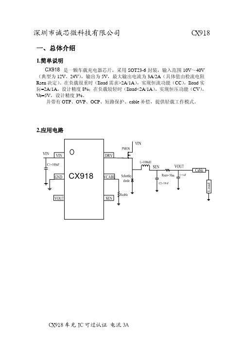
一、总体介绍1.简单说明是一颗车载充电器芯片,采用SOT23-6封装,输入范围10V ~40V (典型为12V 、24V ),输出为5V ,最大输出电流为3A/2A (具体值由检流电阻Rsen 决定)。
在负载很重时(Iload 需求>2A/1A ),实现恒流功能(CC ),Iload 实际=2A/1A ,设计精度8%;在负载较轻时(Iload<2A/1A ),实现恒压功能(CV ),V o=5V ,设计精度3%。
并带有OTP 、OVP 、OCP 、短路保护、cable 补偿,提供轻载工作模式。
2.应用电路CX918深圳市诚芯微科技有限公司 CX918二、测试数据1. 12V/24V 转5V (恒流1A )工作的I/V 曲线负载在1A 以内时,芯片工作在恒压模式下,输出稳定在4.85~5.15V,负载超过1A,输出降低,负载电流恒定供给1A,直到输出拉低到1.5V 左右,芯片关断(短路保护)不工作。
2. 线性调整率和负载调整率:线性调整率4.914.934.954.974.995.015.03101214161820222426283032343638输入电压(V)输出电压(V )Iout=0lout=1ACX918CX918负载调整率4.934.944.954.964.974.984.9955.0100.20.40.60.811.2负载电流(A)输出电压(V )VIN=12V VIN=24V3. 12V 转5V (恒流1A )测试数据及效率图 Vin(V)Iin(A) V out(V) Iout(A)效率 11.89 0.25 2 1.025 68.97% 11.88 0.2942.5 1.027 73.51% 11.84 0.345 3 1.028 75.50% 11.9 0.38 3.5 1.031 79.80% 11.87 0.425 4 1.033 81.91% 11.890.47 4.51.037 83.50%恒流工作效率60.00%65.00%70.00%75.00%80.00%85.00%1.522.533.544.55输出电压(V)效率CX918Vin(V) Iin(A) V out(V) Iout(A)效率 12.02 0.047 5 0.1 88.50% 11.98 0.116 4.98 0.25 89.59% 11.87 0.188 4.98 0.4 89.26% 11.82 0.237 4.97 0.5 88.71% 11.89 0.284 4.96 0.6 88.13% 11.83 0.36 4.96 0.75 87.35% 11.87 0.383 4.95 0.8 87.11% 11.91 0.485 4.941 85.52%恒压工作效率70.00%75.00%80.00%85.00%90.00%95.00%00.20.40.60.81负载电流(A)效率VIN=12V4. 24V 转5V (恒流1A )测试数据及效率图 Vin(V)Iin(A) V out(V) Iout(A) 效率 24.01 0.136 2 1.03 63.09% 24.01 0.158 2.5 1.033 68.08% 24.02 0.18 3 1.035 71.82% 24.02 0.202 3.5 1.037 74.80% 24.01 0.224 4 1.04 77.35% 24.010.2474.51.04579.29%CX918恒流工作效率60.00%65.00%70.00%75.00%80.00%85.00%1.52 2.53 3.54 4.55输出电压(V)效率Vin(V) Iin(A) V out(V) Iout(A)效率 24.03 0.025 5 0.1 83.23% 23.97 0.061 4.99 0.25 85.32% 23.95 0.098 4.98 0.4 84.87% 23.96 0.123 4.98 0.5 84.49% 23.91 0.149 4.97 0.6 83.70% 23.9 0.188 4.96 0.75 82.79% 23.94 0.201 4.96 0.8 82.46% 23.9 0.254 4.95 1 81.54%恒压工作效率70.00%75.00%80.00%85.00%90.00%95.00%00.20.40.60.81负载电流(A)效率VIN=24V三、 PCB 板布局建议:1. 流大电流的线要粗,短,不拐弯。
ME2188 高效 PFM 同步升压 DC-DC 转换芯片说明书

ME2188高效PFM 同步升压DC-DC 转换芯片概述ME2188是一系列高转换效率、低功耗、高工作频率的PFM 同步升压DC-DC 转换芯片。
芯片利用PFM 控制电路,根据负载电流大小自动切换占空比系数,可获得低纹波、高效率、宽输出电压范围的一系列产品。
芯片内置同步开关管及芯片的低消耗电流,有效的提高了DC-DC 的转换效率和设备的使用周期。
外围仅需要三个元件,就可以完成低输入电池电压升压到所需的工作电压。
特点 ● 高效率:93%● 低启动电压: 0.9V @IOUT=1mA ● 低静态电流:7uA ● 频率:320KHz● 可选输出电压:1.9V~5.0V ● 输出精度:±2% ● 输出电流:300mA ● 低纹波、低噪声 ● 同步整流应用场合 封装形式● 1~2节干电池的电子设备 ● 5-pin SOT23-5● 数码相机、LED 手电筒、LED 灯、血压计、 ● 3-pin SOT23、SOT23-3、SOT89-3、TO92 遥控玩具、无线耳机、无线鼠标键盘、医疗器械、汽车防盗器、充电器、VCR 、PDA 等手持电子设备典型应用图LX VOUTGNDME2188VINCIN10uFCOUT 100uFVOUT RLCEL22uF选购指南1. 产品型号说明产品功能:A/C/E/F ME 21 88封装形式:公司标识产品类别产品品种X GX 环保标识M3-SOT23-3M5-SOT23-5X-SOT23P-SOT89-3T-TO92X 产品电压值:33-3.3V产品型号 产品说明ME2188A33M3G V OUT =3.3V ,不带使能端,封装形式:SOT23-3 ME2188C33M5GV OUT =3.3V ,带使能端,封装形式:SOT23-5目前产品的电压值共有11种:2.2V 、2.3V 、2.5V 、2.7V 、2.8V 、3.0V 、3.3V 、3.6V 、3.7V 、4.5V 、5.0V 。
XL6009升压型直流电源变换器芯片(官方版)

n Built in Thermal Shutdown Functionn Built in Current Limit Functionn Available in TO263-5L packageApplicationsn EPC / Notebook Car Adaptern Automotive and Industrial Boost /Buck-Boost / Inverting Convertersn Portable Electronic EquipmentFigure1. Package Type of XL6009Pin ConfigurationsFigure2. Pin Configuration of XL6009 (Top View) Table 1 Pin DescriptionPin Number Pin Name Description1 GND Ground Pin.2 EN Enable Pin. Drive EN pin low to turn off the device, drive it high to turn it on. Floating is default high.3 SW Power Switch Output Pin (SW).4 VIN Supply V oltage Input Pin. XL6009 operates from a 5V to 32V DC voltage. Bypass Vin to GND with a suitably large capacitor to eliminate noise on the input.5 FB Feedback Pin (FB). Through an external resistor divider network, FB senses the output voltage and regulates it. The feedback threshold voltage is 1.25V.Function BlockFigure3. Function Block Diagram of XL6009 Typical Application CircuitFigure4. XL6009 Typical Application Circuit (Boost Converter)to the device. This is a stress rating only and functional operation of the device at these or any other conditions above those indicated in the operation is not implied. Exposure to absolute maximum rating conditions for extended periods may affect reliability.XL6009 Electrical CharacteristicsT a = 25℃;unless otherwise specified.Symbol Parameter Test Condition Min. Typ. Max. Unit System parameters test circuit figure4VFB FeedbackV oltageVin = 12V to 16V, V out=18VIload=0.1A to 2A1.213 1.25 1.287 VEfficiency ŋVin=12V ,V out=18.5VIout=2A- 92 - %Electrical Characteristics (DC Parameters)Vin = 12V, GND=0V, Vin & GND parallel connect a 220uf/50V capacitor; Iout=0.5A, T a = 25℃; the others floating unless otherwise specified.Parameters Symbol Test Condition Min. Typ. Max. Unit Input operation voltage Vin 5 32 V Shutdown Supply Current I STBY V EN=0V 70 100 uAQuiescent Supply Current I q V EN =2V,V FB =Vin2.5 5 mAOscillator Frequency Fosc 320 400 480 Khz Switch Current Limit I L V FB =0 4 AOutput Power NMOS Rdson Vin=12V,I SW=4A110 120 mohmEN Pin Threshold V EN High (Regulator ON)Low (Regulator OFF)1.40.8VI H V EN =2V (ON) 3 10 uA EN Pin Input LeakageCurrent ILV EN =0V (OFF) 3 10 uA Max. Duty Cycle D MAX V FB=0V 90 %Figure5. XL6009 Typical System Application (Boost Converter)Typical System Application for Portable Notebook Car Adapter– SEPIC Buck-Boost Topology (Input 10V~30V, Output 12V/2A)Figure6. XL6009 Typical System Application (SEPIC Buck-Boost Converter) Typical System Application for Inverting Converter– SEPIC Inverting Topology (Input 10V~30V, Output + -12V/1A)Figure7. XL6009 Typical System Application (SEPIC Inverting Converter)Package InformationTO263-5LDimensions In Millimeters Dimensions In Inches SymbolMin Max Min MaxA 4.440 4.650 0.175 0.183B 0.710 0.970 0.028 0.038C 0.360 0.640 0.014 0.025C2 1.255 1.285 0.049 0.051D 8.390 8.890 0.330 0.350E 9.960 10.360 0.392 0.408e 1.550 1.850 0.061 0.073F 6.360 7.360 0.250 0.290L 13.950 14.750 0.549 0.581 L2 1.120 1.420 0.044 0.056。
DCDC电源芯片内部结构全解
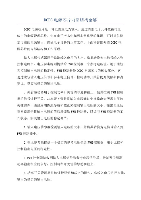
DCDC电源芯片内部结构全解DCDC电源芯片是一种以直流电为输入,通过内部电子元件变换电压输出的电源管理芯片。
它在电子产品中起到非常重要的作用,可以提供稳定可靠的电源输出,保证电子设备的正常工作。
下面将详细介绍DCDC电源芯片的内部结构和工作原理。
输入电压传感器用于监测输入电压的大小,将其转换为电信号输入到控制电路中。
电压参考源则提供给PWM控制器一个参考电压值,用于比较和控制输出电压的稳定性。
PWM控制器是DCDC电源芯片的核心部分,它通过比较输入电压信号和参考电压信号,控制功率开关管的开关频率和占空比,以实现稳定的输出电压。
开关管驱动器用于控制功率开关管的导通和截止,使其按照PWM控制器的信号进行开关。
功率开关管是将输入电压通过变换输出为所需电压的关键部件,通过周期性地导通和截止来控制输出电压的大小。
输出电压反馈回路用于将输出电压的信息反馈给PWM控制器,以调节PWM控制器的工作状态,实现输出电压的稳定调节。
1.输入电压传感器检测输入电压的大小,并将其转换为电信号输入到PWM控制器中。
2.电压参考源提供一个稳定的参考电压值给PWM控制器,用于比较和控制输出电压的稳定性。
3.PWM控制器接收到输入电压信号和参考电压信号后,控制开关管驱动器输出相应的信号,控制功率开关管的导通和截止。
4.功率开关管周期性地进行导通和截止的操作,将输入电压进行变换,输出为稳定的输出电压。
5.输出电压反馈回路将输出电压的信息反馈给PWM控制器,根据反馈信号实时调整PWM控制器的输出信号,实现对输出电压的稳定调节。
通过以上工作原理和内部结构的介绍,可以看出DCDC电源芯片在电子产品中的重要性和作用。
它可以实现对输出电压的稳定调节,保证电子设备的正常工作和运行。
同时,DCDC电源芯片还具有高效能、小体积、低损耗等优点,是电子产品中不可或缺的一部分。
l90工作原理
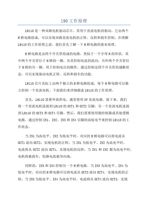
l90工作原理L9110是一种双路电机驱动芯片,常用于直流电机的驱动。
它由两个H桥电路组成,可以实现双路直流电机的正转、反转和刹车控制。
在理解L9110的工作原理之前,我们首先了解一下H桥电路的基本原理。
H桥电路是由四个开关管组成的电路,类似于一个字母H的形状。
其中两个开关管位于H桥的一侧,负责控制电流的流向;另外两个开关管位于H桥的另一侧,用于控制电压的极性。
通过控制这四个开关管的通断状态,可以实现驱动电机正转、反转和刹车的功能。
L9110芯片实际上由两个独立的H桥电路组成,每个H桥电路可以独立控制一个直流电机。
下面我们来详细描述L9110的工作原理。
首先,L9110需要外部供电,通常使用5V直流电源。
接下来,我们将一个直流电机连接到L9110的OUT1和OUT2引脚,另一个直流电机连接到L9110的OUT3和OUT4引脚。
然后,我们需要使用微控制器或其他逻辑电路,通过控制IN1、IN2、IN3和IN4引脚的高低电平来控制L9110的工作状态。
当IN1为高电平、IN2为低电平时,对应的H桥电路可以将电流从OUT1流向OUT2,实现电机的正转;当IN1为低电平、IN2为高电平时,电流将从OUT2流向OUT1,实现电机的反转;当IN1和IN2都为高电平时,电机将被刹车,短路电流被导向地。
同样的,IN3和IN4控制另一个H桥电路。
当IN3为高电平、IN4为低电平时,对应的H桥电路可以将电流从OUT3流向OUT4,实现电机的正转;当IN3为低电平、IN4为高电平时,电流将从OUT4流向OUT3,实现电机的反转;当IN3和IN4都为高电平时,电机将被刹车,短路电流被导向地。
通过控制IN1、IN2、IN3和IN4的高低电平,我们可以实现对两个电机的正转、反转和刹车的控制。
同时,L9110还具有过流保护功能,当电流超过一定阈值时,L9110会自动切断电源,以保护芯片和电机。
总结起来,L9110的工作原理可以归纳为通过控制IN1、IN2、IN3和IN4的高低电平,实现对两个H桥电路的控制,进而控制两个直流电机的正转、反转和刹车。
HX1101 900mA降压芯片
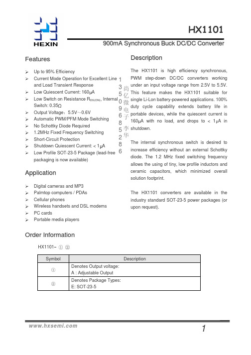
5.5
0.588 0.6 0.612
IFB
∆VFB
Feedback Current VREF
VIN=2.5V~5.5V
±30 0.03 0.4
FOSC Oscillator Frequency
VFB = 0.6V or VOUT = 100%
0.8
1
1.25
IQ
Quiescent Current
VFB = 0.5V or VOUT = 90%, ILOAD = 0A
3 5 0 9 6 8 5
尚 亿 微 电 子
李
under an input voltage range from 2.5V to 5.5V. This feature makes the HX1101 suitable for single Li-Lon battery-powered applications. 100% duty cycle capability extends battery life in portable devices, while the quiescent current is
allows the using of tiny, low profile inductors and
Application
ceramic capacitors, which minimized overall solution footprint.
Digital cameras and MP3
Palmtop computers / PDAs
℃ ~ ℃ Storage Temperature Range ……………………………………………………….- 65
+ 150
XC9303 升压降压转换芯片
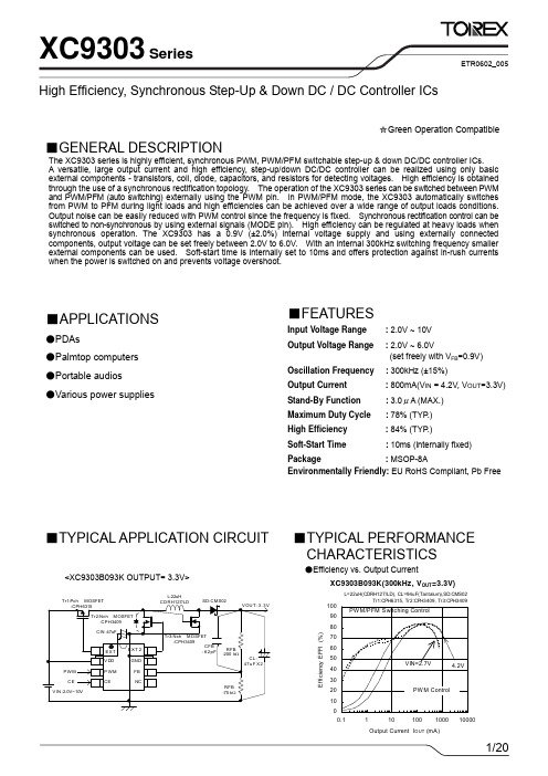
Efficiency EFFI (%)
XC9303B093K(300kHz, VOUT=3.3V)
L=22uH(CDRH127/LD), CL=94uF(Tantalum),SD:CMS02
Tr1:CPH6315, Tr2:CPH3409, Tr3:CPH3409 100
PW M/PFM Switching Control 90
DESIGNATOR ①
ITEM Type of DC/DC Controller
SYMBOL B
DESCRIPTION Standard type
②③
Output Voltage
09
FB Voltage: 0.9V
④
Oscillation Frequency
3
300kHz
⑤⑥-⑦(*1)
Packages (Order Unit)
Ta = 25℃ UNITS
V V V V V mA mW ℃ ℃
3/20
XC9303 Series
■ ELECTRICAL CHARACTERISTICS
XC9303B093
PARAMETER Supply Voltage Maximum Input Voltage Output Voltage Range (*1) Supply Current 1 Supply Current 2 Stand-by Current Oscillation Frequency
Ground
8
EXT2
External Transistor Drive Pin <Connected to Low side of N-ch Power MOSFET Gate>
最简单9v升压电路图大全(四款升压电路原理图详解)
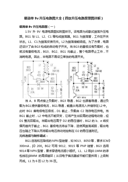
最简单9v升压电路图大全(四款升压电路原理图详解)最简单9v升压电路图(一)1.5V升9V电源电路图如附图所示。
该电路为间歇式振荡升压电路。
BG1与L1、L2、C1等构成振荡器。
BG1为振荡管,工作在开关状态。
L1、C1为振荡反馈元件。
L2为振荡储能绕组。
为了方便,电路还设计了由BG3构成的自动电子开关。
当BG3的基极没有负载时,也就没有基极电流,BG3、BG2、BG1均截止,整个电路停止工作,不消耗电源。
因此,本电路不需设立单独的电源开关。
当A、B两点接上负载时,BG3导通,BG2也跟着导通,通过负载为BG1提供基极电流,BG1导通,能量从电源流入并储存在L2中。
此时BG1集电极电压很低,D1截止,负载由C2残存电压供电。
当BG1截止时,L2中电流不能突变,它将产生出较高的逆程电动势,经D1整流后输出。
当输出电压高于D2的稳压值时,BG2的b、e结反偏而趋向于截止,BG1基极电流将会下降,迫使其振荡减弱,输出电压也随之下降从而将输出电压自动地控制在D2的稳压值附近。
元件选择与制作调试:BG1选饱和压降低的NPN型硅管,如9013、8050等,要求ICM》300mA,β》200。
BG2可用9012、9015等PNP硅管,BG3选用9014等NPN型管,要求穿透电流越小越好。
L1、L2用∮0.1MM的漆包线在∮8MM的高频磁环(从旧电子镇流器或节能灯里拆用)上绕制而成。
L1为6匝L2为36匝。
笔者用此电路为DT890A数字万用表供电,实测工作电流为:蜂鸣挡和电容20uF、2uF挡为45mA以下,其它挡位均在25mA以下。
当电池电压降到0.9V时,除消耗电流较大的蜂鸣挡,电容20uF、2uF 挡有缺电显示外,其余挡位均未见缺电显示。
本电路制作简单,性能稳定,经济实用。
不用调试,只要接线正确,均能正常工作。
数字万用表如果用1.5V电池通过升压替代9V叠层电池,通常都要单独安装电源开关。
给制作和使用带来不便。
HE9116Axx赫尔微DCDC升压芯片
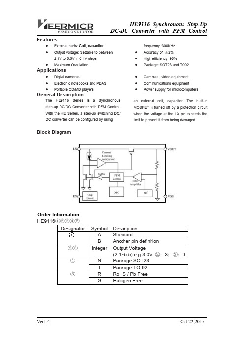
Features●External parts:Coil,capacitor ●Output voltage:Settable to between 2.1V to 5.5V in 0.1V steps ●Maximum Oscillation frequency :300KHz ●Accuracy of ±2%●High efficiency :95%●Package:SOT23and TO92Applications●Digital cameras●Electronic notebooks and PDAS ●Portable CD/MD players●Cameras ,video equipment ●Communications equipment ●Power supply for microcomputersGeneral DescriptionThe HE 9116 Series is a Synchronous step-up DC/DC Converter with PFM Control. With the HE Series, a step-up switching DC/DC converter can be configured by usingan external coil,capacitor.The built-in MOSFET is turned off by a protection circuit when the voltage at the LX pin exceeds the limit to prevent it frombeing damaged.Block DiagramOrder Information HE 9116①②③④⑤DesignatorSymbol Description 1A StandardB Another pin definition ②③Integer OutputVoltage(2.1~5.5)e.g:3.0V=②:3;③:0④N Package:SOT23T Package:TO-92⑤R RoHS /Pb Free G Halogen FreePin AssignmentTable1 HE9116A series(SOT23PKG)PIN NO.PIN NAME FUNCTION1VOUT Output voltage pin2GND GND pin3LX External inductor connection pinTable2 HE9116A series(TO92PKG)PIN NO.PIN NAME FUNCTION1GND GND pin2VOUT Output voltage pin3LX External inductor connection pinTable3 HE9116B series(TO92PKG)PIN NO.PIN NAME FUNCTION1VOUT Output voltage pin2GND GND pin3LX External inductor connection pinAbsolute Maximum Ratings(Unless otherwise specified,Ta=25℃)PARAMETER SYMBOL RATINGS UNITS VOUT Pin Voltage V OUT V SS -0.3~V SS +8V EN Pin Voltage EN V SS -0.3~V SS +8V LX Pin Voltage V LX V SS -0.3~V SS +8V LX Pin CurrentI LX1000mA Power DissipationSOT23PD 250mW SOT23-3/SOT23-5250mW SOT-89-3500mW TO-92500mW Operating Temperature T OPR -40~+85℃Storage Temperature T STG -40~+125℃Soldering Temperature &TimeT SOLDER 260℃,10sNote:These are stress ratings only.Stresses exceeding the range specified under “Absolute MaximumRatings ”may cause substantial damage to the device.Functional operation of this device at other conditions beyond those listed in the specification is not implied and prolonged exposure to extreme conditions may affect device reliability.Electrical Characteristics(Unless otherwise specified ,Ta =25℃)PARAMETER SYMBOL MIN TYP MAX UNITS CONDITIONOutput Voltage V OUT V OUT(S)X0.98V OUT V OUT(S)X1.02V -Input Voltage V IN --7.5V -Operation Start Voltage V ST1--0.9V I OUT =1mA Input Current At No Load I SS1-15-uA V IN =1.8V,V OUT =3.0V Current Consumption 2I SS2-610uA V OUT =V OUT(s)+0.5VCurrent Consumption During Shutdown I SSS -- 1.0uA V EN =0VMaximum OscillationFrequency fosc 300KHzV OUT =0.95xV OUT(s),measureWaveform at LX pin Duty Ratio1Duty1707885%V OUT =0.95xV OUT(s)Efficiency EFF190%Shutdown Pin InputVoltage V SH 0.75--V V OUT =0.95xV OUT(s),judge Oscillation at LX pin V SL --0.3V V OUT =0.95xV OUT(s),judgestop at LX pin Shutdown Pin inputCurrent I SH -0.1-0.1uA V EN =6V I SL-0.1-0.1uAV EN =0VRemark:VOUT(S)specified above is the set output voltage value,and VOUT is the typical value of theactual output voltageApplication CircuitsNote:External Component Recommendation:1)L=47uH(Sumida)2)C=100uF/16V(Tantalum)TYPICAL PERFORMANCE CHARACTERISTICS (Cin=Cout=100uF,L=47uH)Package Information3-pin SOT23Outline Dimensions3-pin TO92Outline Dimensions。
DCDC 电源芯片内部结构全解

作为一名电源研发工程师,自然经常与各种芯片打交道,可能有的工程师对芯片的内部并不是很了解,不少同学在应用新的芯片时直接翻到Datasheet 的应用页面,按照推荐设计搭建外围完事。
如此一来即使应用没有问题,却也忽略了更多的技术细节,对于自身的技术成长并没有积累到更好的经验。
今天以一颗DC/DC 降压电源芯片LM2675 为例,尽量详细讲解下一颗芯片的内部设计原理和结构,IC 行业的同学随便看看就好,欢迎指教!LM2675-5.0 的典型应用电路打开LM2675 的DataSheet,首先看看框图这个图包含了电源芯片的内部全部单元模块,BUCK 结构我们已经很理解了,这个芯片的主要功能是实现对MOS 管的驱动,并通过FB 脚检测输出状态来形成环路控制PWM 驱动功率MOS 管,实现稳压或者恒流输出。
这是一个非同步模式电源,即续流器件为外部二极管,而不是内部MOS 管。
下面咱们一起来分析各个功能是怎么实现的一、基准电压类似于板级电路设计的基准电源,芯片内部基准电压为芯片其他电路提供稳定的参考电压。
这个基准电压要求高精度、稳定性好、温漂小。
芯片内部的参考电压又被称为带隙基准电压,因为这个电压值和硅的带隙电压相近,因此被称为带隙基准。
这个值为1.2V 左右,如下图的一种结构:这里要回到课本讲公式,PN 结的电流和电压公式:可以看出是指数关系,Is 是反向饱和漏电流(即PN 结因为少子漂移造成的漏电流)。
这个电流和PN 结的面积成正比!即Is-》S。
如此就可以推导出Vbe=VT*ln(Ic/Is)!回到上图,由运放分析VX=VY,那么就是I1*R1+Vbe1=Vbe2,这样可得:I1=△Vbe/R1,而且因为M3 和M4 的栅极电压相同,因此电流I1=I2,所以推导出公式:I1=I2=VT*ln(N/R1)N 是Q1 Q2 的PN 结面积之比!回到上图,由运放分析VX=VY,那么就是I1*R1+Vbe1=Vbe2,这样可得:I1=△Vbe/R1,而且因为M3 和M4 的栅极电压相同,因此电流I1=I2,所以推导出公式:I1=I2=VT*ln(N/R1)N 是Q1 Q2 的PN 结面积之比!这样我们最后得到基准Vref=I2*R2+Vbe2,关键点:I1 是正温度系数的,而Vbe 是负温度系数的,再通过N 值调节一下,可是实现很好的温度补偿!得到稳定的基准电压。
DCDC升压转换器(精)
2
5
4
1
3
3
1
TO92 1 2 3
符号
Vss Vout Lx
TO92 1 2 3
符号
Vss Vout Ext
符号
Vss Vout Lx CE NC
符号
Vss Vout Ext CE NC
符号
Vss Vdd Lx Vout NC
引脚描述 接地引脚 输出电压监测,内部电路供电引脚 开关引脚
引脚描述 接地引脚 输出电压监测,内部电路供电引脚 扩流引脚
150
kHz
%
%
主要参数及工作特性
PJ331C Vout=3.3V,Fosc=100kHz
符号
含义
测试条件
最小
数值 典型
VOUT
输出电压
3.218
3.3
VIN
输入电压
Vstart
启动电压
IOUT=1mA, VIN:0→2V
0.8
Vhold
保持电压
IOUT=1mA, VIN:2→0V
0.7
IDD1
输入电流 1
注意:1、Diode 采用肖特基二极管(正向压降约 0.2V),如 IN5817,IN5819
2、电感采用:47μH(r<0.5Ω)
3、电容采用钽电容,47μF。
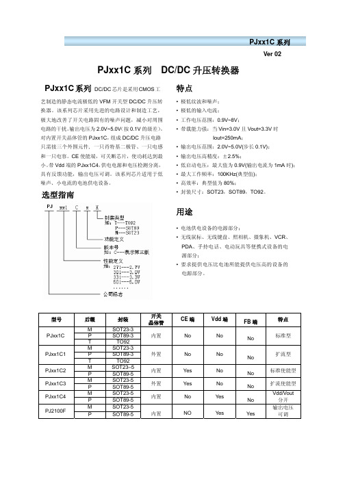
PJxx1C 系列
Ver 02
最大
单位
5.125
V
8
V
0.9
V
V
µA
µA
160
mA
0.5
µA
210
Ω
210
Ω
V
0.3
V
0.5
uA
用XL6009制作一款输出电压可调的大电流DC-DC升压电路
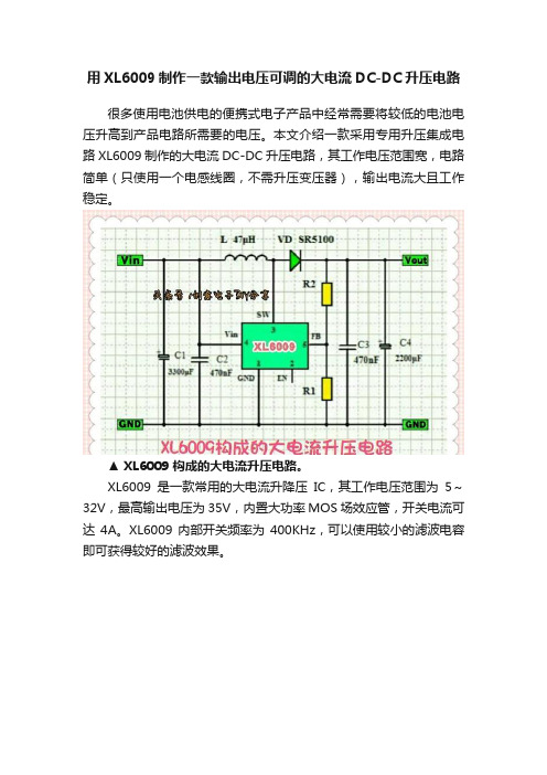
用XL6009制作一款输出电压可调的大电流DC-DC升压电路很多使用电池供电的便携式电子产品中经常需要将较低的电池电压升高到产品电路所需要的电压。
本文介绍一款采用专用升压集成电路XL6009制作的大电流DC-DC升压电路,其工作电压范围宽,电路简单(只使用一个电感线圈,不需升压变压器),输出电流大且工作稳定。
▲XL6009构成的大电流升压电路。
XL6009是一款常用的大电流升降压IC,其工作电压范围为5~32V,最高输出电压为35V,内置大功率MOS场效应管,开关电流可达4A。
XL6009内部开关频率为400KHz,可以使用较小的滤波电容即可获得较好的滤波效果。
▲ TO-263封装的XL6009E1的外形。
XL6009的②脚为使能端,该端为低电平时,XL6009内部电路停止工作无输出,此时整个电路处于低功耗待机状态。
正常工作时该端应为高电平,由于②脚悬空即为高电平,故平时该端为悬空。
XL6009的⑤脚为输出电压采样端,该端外接的电阻R1、R2决定着升压电路的输出电压。
其输出电压Vout=1.25x(1+R2/R1),一般R1可以选用数百Ω至1KΩ的金属膜电阻,R2选用线性电位器来调整输出电压。
上图中的C1~C4为电源滤波电容,其中C1、C4选用普通的铝电解电容,其具体容量可以根据负载电流来选取,C2、C3可以选用高频性能好的独石电容。
▲直插的SR5100肖特基二极管。
上图电路中的二极管VD应选用正向压降小、高频性能好的肖特基二极管,图中用的SR5100肖特基二极管的整流电流为5A,耐压值为100V。
若输出电流不大,亦可以使用3A的SR360肖特基二极管。
▲功率电感的外形。
制作时,升压电感L选用47μH,工作电流≥5A的功率电感。
▲铜散热片。
整个升压电路很简单,制作时全部元件可以焊接在万能板上。
若输出电流较小(数百mA)时,利用XL6009自身散热片散热即可(此时可以在XL6009自身散热片上多焊一些锡)。
TYPE-C PD升压协议全解析

TYPE—C PD升压协议全解析PD是Power Delivery的简称,代表着TYPE—C电力传输的一个通讯协议。
一个简单的TYPE-C PD使用环境,需要下面几个设备构成:HOST、DEVICE、CABLE(即:主机,机,EMARKER)PD的协议书主要的内容集中在:•PD协议的BMC编码规则;•PD协议的4B5B解码;•PD协议的通信流程;•PD协议的通信指令结构;•PD协议的通信内容解析;PD协议独立与USB协议之外,但由于TYPE—C口的兼容特性,可以让PD协议、QC协议、MTK协议、FCP协议等快冲协议熔于一炉。
PD的物理层由发射模块和接收模块组成,由于CC是单线协议,所以所有通信都是半双工的.BMC编码规则是曼切斯特编码的一个版本,按照脉宽来设定的0和1.可以从上图看出,01的编码并不以电平的变化为依据,而是按照脉宽来决定。
BMC的最大频率达330KHz,单指令长度在1ms内.通过逻辑分析仪对波形的读取,我们可以看到未经BMC解码的原码通过BMC从左到右按照脉宽解码后,我们可以得到一系列01的无序组合.通过对01组合的观察,可以看到从左开始有64对01的前导码,来作为数据的等待和除干扰。
64对前导码后,才是需要关注的数据内容。
通过BMC解码后,并去除前导码的数据,也并不是最终可以解析的数据.PD通信协议在这里增加了一个软编码,称为4B5B编码。
即接收到的数据每5个二进制数据,需要经过一个4B5B编码表还原成正确的PD通信数据。
看到这里,都可以想到无线电的加密工作了,但是PD官方资料给出的解释是4B5B是为了降低接收器的设计复杂度并且允许更加多样化的接收器设计。
4B5B的解码表如下:根据图二我们可以做一个4B5B的解码例子:取出图二中引导码后,我们可以得到的数据:00011 0001100011 10001 10010,通过上述4B5B表格进行解码后我们得到最终的数据为:SYNC1-SYNC1—SYNC1-SYNC2-1。
- 1、下载文档前请自行甄别文档内容的完整性,平台不提供额外的编辑、内容补充、找答案等附加服务。
- 2、"仅部分预览"的文档,不可在线预览部分如存在完整性等问题,可反馈申请退款(可完整预览的文档不适用该条件!)。
- 3、如文档侵犯您的权益,请联系客服反馈,我们会尽快为您处理(人工客服工作时间:9:00-18:30)。
XC9119D10A Series1MHz, PWM Controlled,Step-Up DC/DC Converter, Ceramic Capacitor CompatibleETR0408_008■GENERAL DESCRIPTIONThe XC9119D10A series is 1MHz, PWM controlled step-up DC/DC converter, designed to allow the use of ceramic capacitors. With a built-in 2.0Ω switching transistor, the XC9119D10A series can easily provide a step-up operation by using only a coil, a diode, a capacitor, and a resistor, connected externally.Since output voltage up to 19.5V (Maximum Lx operating voltage: 20V) can be derived with reference voltage supply of 1.0V (±2.0%) and external components, the series can easily supply high voltage for various general-purpose power supplies, LCD panels and organic EL displays. With a high switching frequency of 1.0MHz, a low profile and small board area solution can be achieved using a chip coil andan ultra small ceramic output capacitor.With the current limit function (400mA (TYP .): V DD =3.6V), a peak current, which flows through built-in driver transistors can be limited. Soft-start time can be adjusted by external resistors and capacitors. The stand-by function enables the output to be turned off (CE ’L’), that is, the supply current will be less than 1.0⎧A.■TYPICAL APPLICATION CIRCUIT■APPLICATIONS●Organic electroluminescence display (OELD)●Power supplies for LCDs ●Multi-function power supplies■FEATURESOperating Voltage Range : 2.5V ~ 6.0V Output Voltage Range : Up to 19.5V externally set-up: Reference voltage 1.0V +2.0%Oscillation Freq uency : 1.0MHz ±20%ON Resistance : 2.0Ω (V DD =3.6V, V DS=0.4V) Efficiency : 86%(V OUT =15V, V DD =3.6V, I OUT =10mA)Control : PWM control Stand-by function : I STB =1.0⎧A (MAX.)Load Capacitor : Low ESR ceramic capacitorUltra Small Packages : SOT-25, USP-6C Lx Limit Current : 400mA (V DD =3.6V)■TYPICAL PERFORMANCE CHARACTERISTICS○Efficiency vs. Output Current1020304050607080901000.11101001000Output Current: I OUT (mA)E f f i c i e n c y : EF F I (%)XC9119D10A1/182/18■PIN CONFIGURATIONSOT-25*The dissipation pad for the USP-6C package should be solder-plated in recommended mount pattern and metal masking so as to enhance mounting strength and heat resistance. If the pad needs to be connected to other pins, itshould be connected to the V SSpin. USP-6C(BOTTOM VIEW)(TOP VIEW)PIN NUMBER SOT-25 USP-6CPIN NAMEFUNCTION1 2 Lx Switch2 3 V SS Ground 3 1 FB Voltage Feedback 4 6CE/SS Chip Enable/ Soft Start5 4 V DD Power Input - 5NC No Connection■PIN ASSIGNMENT■CE PIN FUNCTIONCE/SS PINOPERATIONAL STATEH OperationL Shut-down ■PRODUCT CLASSIFICATION●Ordering InformationXC9119D ①②③④⑤-⑥(*1)DESIGNATOR DESCRIPTION SYMBOLDESCRIPTION①② Reference Voltage 10 FB voltage ③Oscillation FrequencyA1MHzMR SOT-25MR-G SOT-25 (Halogen & Antimony free)ER USP-6C ④⑤-⑥Packages Taping Type(*2)ER-GUSP-6C (Halogen & Antimony free)(*1)The “-G” suffix indicates that the products are Halogen and Antimony free as well as being fully EU RoHS compliant. (*2)The device orientation is fixed in its embossed tape pocket. For reverse orientation, please contact your local Torex sales office or representative. (Standard orientation: ④R-⑥, Reverse orientation: ④L-⑥)XC9119D10ASeries ■BLOCK DIAGRAMVDDL X FBVSS■ABSOLUTE MAXIMUM RATINGSTa = 25O CPARAMETER SYMBOL RATINGS UNITSV DD Pin Voltage V DD V SS – 0.3 ~ 7.0 VLx Pin Voltage V Lx V SS – 0.3 ~ 22.0 VFB Pin Voltage V FB V SS – 0.3 ~ 7.0 VCE Pin Voltage V CE V SS – 0.3 ~ 7.0 VLx Pin Current I Lx 1000 mASOT-25 250 Power Dissipation Pd mWUSP-6C 120Operating Temperature Range Topr - 40 ~ + 85 O CStorage Temperature Range Tstg - 55 ~ +125 O C3/18■ELECTRICAL CHARACTERISTICSXC9119D10AMR4/18PARAMETER SYMBOLCONDITIONSMIN.TYP .MAX.UNITCIRCUITTa = 25O CFB Voltage V FB - 0.980 1.000 1.020 V ① △V FB/Line Regulation 2.5<△V IN ・V FBV DD <6.0V - 0.05 0.20 %/V ①Supply Voltage V DD - 2.5 - 6.0 V ① Operation Start-upVoltageV ST1 I OUT =0mA - - 2.5 V ② Supply Current 1 I DD1 - 450 700 μA ② FB=2.0VSupply Current 2 I DD2 - 55 110 μA ②Stand-by Current I STB V CE =0V - - 1.0 μA ③ Oscillation Frequency f Same as I DD1 0.8 1.0 1.2 MHz ② OSCMaximum Duty RatioMAXDTYSame as I DD1 86 92 98 % ② Efficiency (*1) EFFIV IN =V DD =3.6V, V OUT =15V,I OUT =10mA- 86 - % ① Current Limit I LIM V DD =3.6V 310 400 750 mA ④ Lx Operating VoltageRangeV Lx V OUT =18V - - 20.0 V ①Lx Switch On Resistance R SWON V DD =3.6V, V Lx =0.4V, Rpull=10Ω- 2.0 4.0 Ω ②Lx Leak Current I LxL Same as I STB - - 1 μA ③Applied voltage to CE when Lx pinvoltage holding “H””L” level CE “High” Voltage V CEH 0.65 - - V ②Applied voltage to CE when Lx pinvoltage holding “H” levelCE “Low” Voltage V CEL - - 0.20 V ②Soft-Start FB=0.95V , Applied voltage to CEV SST 1.3 1.6 1.9 V ②when Lx voltage holding “H””L” level Threshold VoltageCE “High” Current I CEH Same as I DD2 -0.1 - 0.1 μA ③ CE “Low” Current I CEL Same as I STB -0.1 - 0.1 μA ③ FB “High” Current I FBH Same as I DD2 -0.1 - 0.1 μA ③ FB “Low” Current I FBL Same as I STB -0.1 - 0.1 μA ③Test Condition: Unless otherwise stated, V IN =3.0V, V CE =3.0V, Vpull=5.0V, Rpull=100Ω.NOTE:*1: EFFI={(output voltage x output current) / (input voltage) x (input current)} x 100 ■TYPICAL APPLICATION CIRCUITV IN VOUT5/18XC9119D10ASeries■OPERATIONAL EXPLANATIONThe XC9119D10A series consists of a reference voltage source, ramp wave circuit, error amplifier, PWM comparator, phasecompensation circuit, driver transistor, current limiter circuit and others. The series ICs compare, using the error amplifier, the voltage of the internal reference voltage source with the feedback voltage from the FB pin. Phase compensation is performedon the resulting error amplifier output, to input a signal to the PWM comparator to determine the turn-on time during switching. The PWM comparator compares, in terms of voltage level, the signal from the error amplifier with the ramp wave from the ramp wave circuit, and delivers the resulting output to the buffer drive circuit to cause the Lx pin to output a switching duty cycle. This process is continuously performed to ensure stable output voltage. The current feedback circuit detects the N-channel MOS driver transistor's current for each switching operation, and modulates the error amplifier output signal to provide multiple feedback signals. This enables a stable feedback loop even when a low ESR capacitor, such as a ceramic capacitor, is used, ensuring stable output voltage.<Reference Voltage Source>The reference voltage source provides the reference voltage to ensure stable output voltage of the IC.<Ramp Wave Circuit>The ramp wave circuit determines switching frequency. The 1MHz (TYP .) of frequency is fixed internally. Clock pulses generated in this circuit are used to produce ramp waveforms needed for PWM operation.<Error Amplifier>The error amplifier is designed to monitor output voltage. The amplifier compares the reference voltage with the FB pin voltage. When a voltage lower than the reference voltage is fed back, the output voltage of the error amplifier increases. Gain and frequency characteristics of the error amplifier output are fixed internally as an optimize signal. <Current Limit >The current limit circuit of the XC9119D10A series monitors the current flowing through the N-channel MOS driver transistor connected to the Lx pin, and features a combination of the constant-current type current limit mode and the duty cycle limit of the next pulse.①When the driver current is greater than a specific level, the constant-current type current limit function operates to turn off the pulses from the Lx pin at any given timing.②The IC controls the next pulse to be smaller than the first pulse.Current Limit Current Limit21LxILThe current will be off when the coil current reaches the value of the constant current limit.Limit some duty pulses after the limit.<CE Pin Function>The operation of the XC9119D10A series will enter into the shut down mode when a low level signal is input to the CE pin. During the shut down mode, the supply current is 0μA (TYP .), with high impedance at the Lx pin. The IC starts its operation with a high level signal to the CE pin. The input to the CE pin is a CMOS input and the sink current is 0μA (TYP .). The hysteresis between the chip enable and the chip disable is 50mV (TYP .). <Soft-Start Time>Soft-start function operates when capacitors and resistors are connected to the CE/SS pin. With the Vref voltage limited by the CE/SS pin start-up voltage and applying the input to the error amps, the operation maintains a balance between the two inputs of the error amps. and controls the Lx pin’s ON time so that it doesn’t increase more than is necessary. Depending of current limit function, load current, step-up ratio, and external components, the IC takes about 500uS to 5mS to attain the setting voltage after applying the CE ‘H’ voltage even though the R SS is 0Ω and a soft start capacitor C SS is not connected. (For a numerical constant, please refer to Note on Use.) For longer soft-start time, please connect R SS and C SS . Soft-start function operates while the CE pin voltage is between 0V to around 1.9V . Please be noted that if the CE/SS pin voltage does not start from 0V but is in intermediate potential when the power is turned on etc., soft start function may lose an effect and that will cause a high inrush current and ripple voltage.■OPERATIONAL EXPLANATION (Continued)<CE/SS (Pin No. 4): Chip Enable / Soft-Start Pin>Pin No. 4 can be used as in either chip enable (CE) pin or soft-start (SS) pin. The IC takes about 5ms at most to attain the setting voltage after starting operation (CE ‘H’) even though the R SS is 0Ω and the C SS is not connected.Soft-start function is good for setting a longer time than the start-up time when the R SS is 0Ω and the C SS is not connected. Soft-start operates while the CE pin voltage increases from 0V to around 1.9V . The following equation is used with the values of Vcont voltage, the R SS and the C SS . T = - C SS x R SS x In {(Vcont – 1.6) / Vcont}R SS =0Ω, No C SS , V IN =3.6V, V OUT =15V, I OUT =3mA1ch: V OUT2ch: CE0V (1ch) ⇒0V (2ch) ⇒Time:500uS/div.1ch:5V/div., 2ch:2V/div.●Start-up waveformwhen the R SS is 0Ω and the C SS is not connectedEx.) When C SS =0.1uF, R SS =220k Ω, Vcont=5V,T= - 0.1e – 6 x 220e3 x In{(5-1.6)/5} = 8.48msEx.) Reference Circuit 1: N-ch Open DrainON/OFF SignalCE/SS PinEx.) Reference Circuit 2: CMOS Logic (Low Supply Current)ON/OFF SignalCE/SS PinEx.) Reference Circuit 3: CMOS Logic (Low Supply Current), Quick-OffON/OFF SignalCE/SS Pin6/187/18XC9119D10ASeries■OPERATIONAL EXPLANATION (Continued)<Lx (Pin No. 1): Switch Pin>Please connect the anode of an Schottky barrier diode and inductor to the Lx pin. <FB (Pin No. 3): Voltage Feedback Pin>The reference voltage is 1.0V (TYP .). Output voltage is approximated by the following equation according to the value for two resistors (R FB1 and R FB2). The sum of the two resistors should be 1M Ω or less. V OUT = R FB1 / R FB2 + 1Output voltage should be set as to fill V OUT <(Maximum value of V Lx ) – (V F of Schottky diode).Please adjust the C FB value of the speed–up capacitor for phase compensation so that fzfb=1/(2πx C FB x R FB1) will be about 500Hz. According to the usage, adjusting the inductance value, the load capacity value, and so on to the most suitable operation.Typical example:V OUT R FB1 R FB2 C FB (V)(k Ω)(k Ω)(pF)3.3 300 130 1000 5.0 300 75 1000 7.0 180 30 1800 10.0 270 30 1200 15.0 510 36 510 18.0 510 30510<V DD (Pin No. 5): Power Supply Pin>Please connect an input by-pass capacitor (C IN ).●Application Information<Obtaining V DD from other source than V IN >In case that the input voltage V IN and power source V DD in the step-up circuit are isolated, the circuit starts step-up operations with the input voltage less than 2.5V when voltage from 2.5V to 6.0V is applied to the power source. Please connect more than 1uF of C DD between the V DD pin and the V SS pin as close as possible.Ex.) When VDD =3.6V, V IN =1.8V, V OUT =5.0V (R FB1=300k Ω, R FB2=75k Ω, C FB =1000pF, C L =10μF), the IC can operate upto I OUT =40mA.■NOTES ON USE1. Please do not exceed the value of stated absolute maximum ratings.2. The DC/DC converter performance is greatly influenced by not only the ICs’ characteristics, but also by those of the external components. Care must be taken when selecting the external components.3. Make sure that the PCB GND traces are as thick as possible, as variations in ground potential caused by high ground currents at the time of switching may result in instability of the IC.4. Please mount each external component as close to the IC as possible and use thick, short connecting traces to reduce the circuit impedance.5. Please set up the output voltage value so that the Lx pin voltage does not exceed 20V.■TEST CIRCUITS Circuit ①Circuit ②Circuit③V IN LxCE FBV SSAV1uFV FB220uFRpullOSCVCircuit ④VV IN10300Ω1. The measurement method of Lx On resistance R SWONUsing the circuit ②, Lx On resistance can be measured by adjusting Vpull voltage to set Lx voltage V Lx x 0.4V when the driver transistor is ON. The oscilloscope is used for measuring the Lx voltage when the driver transistor is ON.R SWON = 0.4 / {(Vpull – 0.4) / 10}2. The measurement method of current limit I LIMUsing the circuit ④, current limit I LIM can be calculate by the equation including Vpull voltage when FB voltage is decreased while Vpull voltage is adjusted and Lx voltage V Lx when the driver transistor is ON. The oscilloscope is used for measuring the Lx voltage when the driver transistor is ON.I LIM=(Vpull – V Lx) / Rpull8/189/18XC9119D10ASeries■TYPICAL PERFORMANCE CHARACTERISTICS(1) Output Voltage vs. Output Current9.09.510.010.511.00.11101001000Load current: I OUT (mA)O u t p u t v o l t a g e : V O U T (V )VIN=VDD=VCE,L=22uH(CDRH4D18C)SD:XBS104S14R,CIN=CL=4.7uF(Ceramic)4.74.84.95.05.15.25.30.11101001000Load current: I OUT (mA)Ou t p u t v o l t a g e : V O U T (V )VIN=VDD=VCE,L=4.7uH(CDRH4D18C)SD:XBS104S14R,CIN=CL=4.7uF(Ceramic)17.017.518.018.519.00.11101001000Load current: I OUT (mA)O u t p u t v o l t a g e : VO U T (V )VIN=VDD=VCE,L=22uH(CDRH4D18C)SD:XBS104S14R,CIN=CL=4.7uF(Ceramic)14.014.515.015.516.00.11101001000Load current I OUT (mA)O u t p u t v o l t a g e : V OU T (V )VIN=VDD=VCE,L=22uH(CDRH4D18C)SD:XBS104S14R,CIN=CL=4.7uF(Ceramic)(2) Efficiency vs. Output CurrentVOUT=5VVOUT=10V1020304050607080901000.11101001000Load current: I OUT (mA)E f f i c i e n c y : EF F I (%)VIN=VDD=VCE,L=4.7uH(CDRH4D18C)SD:XBS104S14R,CIN=CL=4.7uF(Ceramic)0.11101001000Load current: I OUT (mA)E f f i c i e n c y : EF F I (%)VIN=VDD=VCE,L=22uH(CDRH4D18C)SD:XBS104S14R,CIN=CL=4.7uF(Ceramic)■TYPICAL PERFORMANCE CHARACTERISTICS (Continued)(2) Efficiency vs. Output Current (Continued)VOUT=18VVOUT=15V1020304050607080901000.11101001000Load current: I OUT (mA)E f f i c i e n c y : EF F I (%)VIN=VDD=VCE,L=22uH(CDRH4D18C)SD:XBS104S14R,CIN=CL=4.7uF(Ceramic)1020304050607080901000.11101001000Load current: I OUT (mA)E f f i c i e n c y : EF F I (%)VIN=VDD=VCE,L=22uH(CDRH4D18C)SD:XBS104S14R,CIN=CL=4.7uF(Ceramic)VOUT=15VVOUT=15V01020304050607080901000.11101001000Load current: I OUT (mA)E f f i c i e n c y :E F F I (%)VIN=VDD=VCE=3.6V,L :CDRH4D18C SD:XBS104S14R,CIN=CL=4.7uF(Ceramic)1020304050607080901000.1110100Load current: I OUT (mA)E f f i c i e n c y :E F F I (%)VIN=VDD=VCE=3.6V,L =22uHSD:XBS104S14R,CIN=CL=4.7uF(Ceramic)(3) Ripple Voltage vs. Output CurrentVOUT=5VVOUT=10V10/18204060801000.11101001000Load current: I OUT (mA)R i p p l e V o l t a g e : V r (m V )VIN=VDD=VCE,L=4.7uH(CDRH4D18C)SD:XBS104S14R,CIN=CL=4.7uF(Ceramic)0.11101001000Load current: I OUT (mA)R i p p l e V o l t a g e : V r (m V )VIN=VDD=VCE,L=22uH(CDRH4D18C)SD:XBS104S14R,CIN=CL=4.7uF(Ceramic)11/18Series■TYPICAL PERFORMANCE CHARACTERISTICS (Continued)(3) Ripple Voltage vs. Output Current (Continued)VOUT=18VVOUT=15V204060801000.11101001000Load current: I OUT (mA)R i p p l e V o l t a g e : V r (m V )VIN=VDD=VCE,L=22uH(CDRH4D18C)SD:XBS104S14R,CIN=CL=4.7uF(Ceramic)0204060801000.11101001000Load current: I OUT (mA)R i p p l e V o l t a g e : V r (m V )VIN=VDD=VCE,L=22uH(CDRH4D18C)SD:XBS104S14R,CIN=CL=4.7uF(Ceramic)(4) Maximum Output Current vs. Input Voltage (5) Feedback Voltage vs. Chip Enable Voltage050100150200250300350400450234567Input Voltage V IN (V)M a x i m u m l o a d c u r r e n t :I O U T _M A X (m A )VIN=VDD=VCE=3.6V,SD:XBS104S14R 0.00.20.40.60.81.01.200.51 1.52Chip E nable Voltage: V CE (V)F e e d b a c k V o l t a g e : V F B (V )(6) Supply Current 1 vs. Supply Voltage(7) Supply Current 2 vs. Supply Voltage02004006008001000120023456Supply Voltage: V DD (V)S u p p l y C u r r e n t 1: ID D 1(uA )02040608010012014023456Supply Voltage: V DD (V)S u p p l y C u r r e n t 2: ID D 2(uA )■TYPICAL PERFORMANCE CHARACTERISTICS (Continued)(9) Maximum Duty Cycle vs. Supply Voltage(8) Oscillation Frequency vs. Supply Voltage0.60.70.80.911.11.21.323456Supply Voltage: V DD (V)O s c i l l a t i o n F r e q u e n c y : F o s c (M H z )8688909294969823456Supply Voltage: V DD (V)M a x i m u m D u t y C y c l e : M A X D T Y (%)(10) Stan-by Current vs. Supply Voltage (11) Lx ON Resistance vs. Supply Voltage0.00.20.40.60.81.023456Supply Voltage: VDD (V)S t a n d b y C u r r e n t : IS T B (uA )0.01.02.03.04.05.06.023456Supply Voltage: V DD (V)L x O N R e s i s t a n c e : RS WO N(Ω)(12) Current Limit vs. Supply Voltage (13) Feedback Voltage vs. Supply Voltage12/18010020030040050060070080090023456Supply Voltage: V DD (V)C u r r e n t L i m i t : IL I M (m A )13/18Series■TYPICAL PERFORMANCE CHARACTERISTICS (Continued)(14) CE ‘H’ Voltage vs. Supply Voltage(15) CE ‘L’ Voltage vs. Supply Voltage0.200.250.300.350.400.450.500.550.600.6523456Supply Voltage: V DD (V)C E 'H ' V o l t a g e : VC E H (V )0.200.250.300.350.400.450.500.550.600.6523456Supply Voltage: VDD(V)C E 'L ' V o l t a g e : V C E L (V )VFB=0V,Vpull=5V,Rpull=100 (16) Load Transient Response4.804.854.904.955.005.055.10Time (0.2msec/div)O u t p u t V o l t a g e : V O U T (V )102030405060L o a d c u r r e n t :I O U T (m A )VIN=VDD=VCE=3.6V,L :CDRH4D18C SD:XBS104S14R,CIN=CL=4.7uF(Ceramic)CFB=620pF(Ceramic),RFB1=510k ohm,RFB2=36k ohm4.804.854.904.955.005.055.10Time (1.0msec/div)O u t p u t V o l t a g e : V O U T (V )102030405060L o a d c u r r e n t :I O U T (m A )VIN=VDD=VCE=3.6V,L :CDRH4D18C SD:XBS104S14R,CIN=CL=4.7uF(Ceramic)14.8014.8514.9014.9515.0015.0515.10Time (2.0msec/div)O u t p u t V o l t a g e : V O U T (V )102030405060L o a d c u r r e n t :I O U T (m A )VIN=VDD=VCE,L=4.7uH(CDRH4D18C)SD:XBS104S14R,CIN=CL=4.7uF(Ceramic)14.8014.8514.9014.9515.0015.0515.10Time (0.5msec/div)O u t p u t V o l t a g e : V O U T (V )102030405060L o a d c u r r e n t :I O U T (m A )VIN=VDD=VCE,L=4.7uH(CDRH4D18C)SD:XBS104S14R,CIN=CL=4.7uF(Ceramic)■TYPICAL PERFORMANCE CHARACTERISTICS (Continued)(17) Maximum Output Current vs. Input Voltage020*********120140160123456Input Voltage VIN(V)M a x i m u m O u t p u t C u r r e n t :IO U T _M A X (m A )SD:XB01B04ABR,L=22uH(CDRH4D18C)VCE=VDD,CIN=4.7uF(Ceramic)CL=10uF(Ceramic)CFB=620pF(Ceramic),RFB1=510k ,RFB2=36k 0100200300400500123456Input Voltage VIN(V)M a x i m u m O u t p u t C u r r e n t : I O U T _M A X (m A )SD:XB01B04ABR,L=4.7uH(CDRH4D18C)VCE=VDD,CIN=4.7uF(Ceramic)CL=10uF(Ceramic)VOUT=5VVOUT=15V14/1815/18Series■PACKAGING INFORMATION●SOT-25●USP-6C■PACKAGING INFORMATION (Continued)●USP-6C Reference Pattern Layout ●USP-6C Reference Metal Mask Design16/18Series■MARKING RULE●SOT-25 ①represents product seriesMARK PRODUCT SERIESXC9119xxxxMxL②represents Lx overvoltage limitMARK Lx OVERVOLTAGE LIMIT PRODUCT SERIESD NotAvailableXC9119DxxxMx SOT-25(TOP VIEW)③represents oscillation frequencyMARK OSCILLATION FREQUENCY PRODUCT SERIESA 1MHz XC9119xxxAMx④represents production lot number0 to 9 and A to Z, or inverted characters 0 to 9 and A to Z repeated.(G, I, J, O, Q, W excepted)●USP-6C①represents product seriesMARK PRODUCT SERIESV XC9119xxxxDx②represents Lx overvoltage limitMARK Lx OVERVOLTAGE LIMIT PRODUCT SERIESD NotAvailable XC9119DxxxDx USP-6C ③④represents FB voltage(TOP VIEW)MARK③FB VOLTAGE (V) PRODUCT SERIES④1 0 1.0 XC9119x10xDx⑤represents oscillation frequencyMARK OSCILLATION FREQUENCY PRODUCT SERIESA 1MHz XC9119xxxADx⑥represents production lot number0 to 9 and A to Z repeated (G, I, J, O, Q, W excepted)* No character inversion used.17/1818/18。