100mA同步降压型转换器
基于DPLL同步的高频降压型DC—DC转换器设计

Ab s t r a c t :Th i s p a p e r p r e s e n t s a d e s i g n o f d i g i t a l p h a s e — l o c k e d l o o p( DPLL) s y n c h r o n i z e d h i g h — f r e q u e nc y h y s t e r e t i c c o n t r o l DC— DC b u c k c o n v e r t e r . Di g i t a l p h a s e — l o c k e d l o o p o p e r a t i o n i s l o c k e d t o t h e r e f e r e n c e c l o c k f r e q u e n c y ,a n d d i g i t a l c o nt r o l d e l a y l i n e( DCDL)i s u s e d t o e l i mi n a t e t h e d u t y c y c l e ’ S ,a n d h e n c e t h e
最近 1 0年 , 嵌 入 式 技 术 促 进 便 携 式 电子 产 品 以
惊人 的 速 度 迅 猛 发 展 和 普 及 。 目前 , 高效 能、 高 精 度、 微体积的 D C — D C转 换 器 成 为 除 高 效 能 电池 以 外 制 约 小 型 轻 量 高 档 便 携 式 电子 产 品进 ~ 步 发 展 的瓶
o n DP L L s y n c h r o n i z a t i o n
Mu Ni a n q i a ng
( De p a r t me n t o f El e c t r i c a l En g i n e e r i n g ,S h a n d o n g Al u mi n u m Vo c a t i o n a l Co l l e g e ,Z i b o 2 5 5 0 6 5,Ch i n a )
降压型电源转换IC LP3221DC-DC
DC/DC降压型电源转换IC LP3220
1.5MHZ,1300mA,高效率,同步PSM/PWM 降压DC/DC 带软启动电源转换IC 概述
LP3220是一款具有恒定频率恒定电流带PWM模式控制的降压驱动IC。
可在单节锂电池供电情况下达到带载大电流1A且效率保持在95%以上。
LP3220同时在压差极小情况下可达到100%工作占空比,在轻载条件有极小的纹波与噪声,大大延长锂电池的使用寿命。
LP3220在2.5V至5.5V输入电压情况下,可达到带载电流1.3A,且最低输出电压可至0.6V。
极高的工作频率可使外围元器件尽可能的小,非常适合便携式电子设备。
内置的斜坡补偿器可使电感值尽可能小且保持较高工作效率。
LP3220工作输出电压可调节(0.6V至输入电压值). 产品绿色环保无不含铅, sot23-5 封装可使芯片工作在-40℃至85℃。
其他功能还包括软启动, 较低的内部参考电压,精确率达到2%, 超温保护和过电流保护。
特点
◆效率高达96%
◆1.5MHz 校正频率PWM工作
◆可调输出电压0.6V 至VIN
◆1300mA 输出电流
◆无外部肖特基二极管需求
◆低压差工作时100% 工作占空比
◆可选SOT23-5/TSOT23-5 封装
◆短路保护与过温保护
◆过压保护
◆低于1µA 关断电流
应用领域
◆便携音频播放器/MP3 播放器
◆手机
◆PDA
◆DSC
◆无线网卡。
PT1202-电流模式同步降压型稳压器
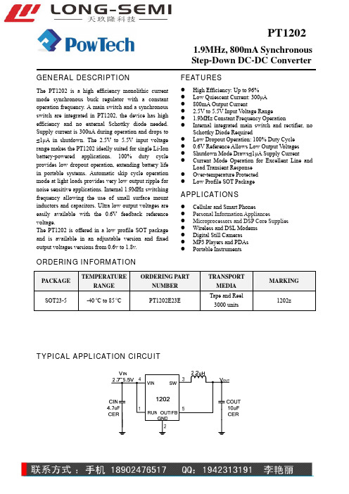
Step-Down DC-DC ConverterGENERAL DESCRIPTIONThe PT1202 is a high efficiency monolithic current mode synchronous buck regulator with a constant operation frequency. A main switch and a synchronous switch are integrated in PT1202, the device has high efficiency and no external Schottky diode needed. Supply current is 300uA during operation and drops to ≤1μA in shutdown. The 2.5V to 5.5V input voltage range makes the PT1202 ideally suited for single Li-Ion battery-powered applications. 100% duty cycle provides low dropout operation, extending battery life in portable systems. Automatic skip cycle operation mode at light loads provides very low output ripple for noise sensitive applications. Internal 1.9MHz switching frequency allowing the use of small surface mount inductors and capacitors. Ultra low output voltages are easily available with the 0.6V feedback reference voltage.The PT1202 is offered in a low profile SOT package and is available in an adjustable version and fixed output voltages versions from 0.6v to 1.8v.FEATURESz High Efficiency: Up to 96% z Low Quiescent Current: 300μA z 800mA Output Currentz 2.5V to 5.5V Input V oltage Rangez 1.9MHz Constant Frequency Operationz Internal integrated main switch and rectifier, no Schottky Diode Requiredz Low Dropout Operation: 100% Duty Cycle z 0.6V Reference Allows Low Output V oltages z Shutdown Mode Draws ≤1μA Supply Current z Current Mode Operation for Excellent Line and Load Transient Response z Over-temperature Protected zLow Profile SOT PackageAPPLICATIONSz Cellular and Smart Phonesz Personal Information Appliancesz Microprocessors and DSP Core Supplies z Wireless and DSL Modems z Digital Still Cameras z MP3 Players and PDAs zPortable InstrumentsORDERING INFORMATIONPACKAGETEMPERATURERANGEORDERING PARTNUMBERTRANSPORT MEDIAMARKING SOT23-5 -40 o C to 85 o C PT1202E23ETape and Reel 3000 units1202zTYPICAL APPLICATION CIRCUITStep-Down DC-DC ConverterPIN ASSIGNMENTPIN DESCRIPTIONSPINNAMES PIN No. DESCRIPTIONRUN 1 Chip Enable, Active with ‘H’GND 2 Chip Ground SW3Output of Internal SwitchesVIN 4 Power SupplyV FB /V OUT 5 Regulated Feedback/Output V oltageABSOLOUTE MAXIMUM RATING (Note1)SYMBOL ITEMSVALUEUNITV IN Input Supply V oltage – 0.3 to 6 V V RUN RUN Pin V oltage – 0.3 to VIN V V FB FB Pin V oltage – 0.3 to VIN VV SW SW Pin V oltage– 0.3 to (VIN + 0.3)V I SW SW Pin Source/Sink Current (DC) ±1 A I SW SW Pin Source/Sink Current (peak)±1.5AT J Junction Temperature 125 °C T OPER Operating Temperature Range – 40 to 85 °CT STG Storage Temperature Range– 65 to 150°CT SOLDER Lead Temperature (Soldering, 10 sec)300 °CθJAThermal Resister220°C/WNote1: Absolute Maximum Ratings are those values beyond which the life of the device maybe impaired.Step-Down DC-DC ConverterELECTRICAL CHARACTERISTICSTA = 25°C. VRUN=VIN = 3.6V unless otherwise specified.SYMBOL PARAMETER CONDITIONS MIN TYP MAX UNITS V FB Regulated Feedback Voltage T A=25℃0.5880.600 0.612 V ∆V FB LineRegulation V IN = 2.5V to 5.5V 0.04 0.5 %/VI FB VFB Input Bias Current 0 ±30 nAI PK PeakInductor Current V IN = 3V, V FB = 0.5V, DutyCycle < 35%1 AV LOADREG LoadRegulation 0.5 % V IN InputVoltageRange 2.5 5.5 VI S Input DC Bias CurrentActive ModeShutdownV FB = 0.5V or V OUT = 90%,I LOAD = 0AV RUN = 0V, VIN = 4.2V3000.14001µAF OSC OscillatorFrequencyV FB = 0.6V or VOUT = 100% 1.5 1.9 2.3 MHzR PFET RDS(ON) of P-ChannelFETI SW = 100mA 0.4 0.5 ΩR NFET RDS(ON) of N-Channel FET I SW = –100mA 0.35 0.45 ΩI LSW SWLeakage V RUN = 0V, V SW = 0V or 5V,V IN = 5V±0.01 ±1 µAV RUN RUNThresholdVoltage-40℃≤T A≤ 85℃0.3 1.0 1.50 V Note: The Min and Max value is guaranteed by final test or lab statistic.Step-Down DC-DC ConverterSIMPLIFIED BLOCK DIAGRAMOPERATION DESCRIPTIONThe PT1202 is a high efficiency monolithic current mode synchronous buck regulator with a constant operation frequency. Its internal integrated MOSFETs achieve high efficiency. Ultra low output voltages are easily available with the 0.6V feedback reference voltage. Internal fixed 1.9MHz switching frequency allowing the use of small surface mount inductors and capacitors. The 2.5V to 5.5V input voltage range and 800mA output current make the PT1202 ideally suited for single Li-Ion battery-powered applications.Current Mode PWM Control LoopSlope compensated current mode PWM control and cycle-by-cycle current limit provides stable operation and excellent line and load regulation. During normal operation, the internal top power MOSFET is turned on each cycle when the rising edge of the oscillator sets the RS latch, and turned off when rising edge of the PWM comparator resets the RS latch. While the top MOSFET is off, the bottom MOSFET is turned on until either the inductor current starts to reverse or the beginning of the next clock cycle. The OVDET comparator controls output transient overshoots is smaller than 8% by turning the main MOSFET off until the fault is removed.Skip-Cycles Mode OperationAt light loads, the PT1202 enters skip-cycle mode automatically. In this mode, the inductor current may reach zero or reverse on each cycle. The PWM control loop will automatically skip cycles to maintain output regulation. The bottom MOSFET is turned off by thecurrent reversal comparator, IR-CMPARATOR, and the switch voltage will ring. This is discontinuous mode operation, and is normal behavior for the switching regulator.Current Fold-Back OperationThe frequency of the oscillator is reduced to about 210 KHz when the output voltage is smaller than 50% of normal value; which ensures the inductor current has more time to decay, thereby preventing runaway. The oscillator’s frequency will progressively increase to 1.9MHz when the output voltage rises above 50%. Low-Dropout OperationWhen the input voltage deceases to the value of output voltage, the control loop remains the main MOSFET on until it reaches 100% duty cycle. The output voltage then is the input voltage minus the voltage drop across the main switch and the inductor. Caution must be exercised to ensure the heat dissipated not to exceed the maximum junction temperature of the IC because the RDSON of the main MOSFET increases and the efficiency of the converter decrease.Maximum Load CurrentThe PT1202 operates with input voltage as low as 2.5V. However, the maximum load current decreases when the input voltage deceases because of the large IR drop of the main switch and the synchronous switch. And the slope compensation reduces the peak inductor current.Step-Down DC-DC ConverterChina Resources Powtech (Shanghai) Limited Page 5PT1202_DS Rev EN_3.1TYPICAL PERFORMANCE CHARACTERISTICS(From Figure 1, TA=25 Unless Otherwise Specified)℃Efficiency vs. Input VoltageEfficiency vs. Output Current0.5110100700O utput C urrent (m A)Efficiency vs. Output Current0.500.550.600.650.700.750.800.850.900.95Output Current (mA)E f f i c i e n c yEfficiency vs. Output CurrentOutput Current (mA)Reference Voltage (V) vs. Temperature (℃) Oscillator Frequency vs. VINStep-Down DC-DC ConverterOscillator Frequency vs. Temperature (℃)Supply Current vs. Temperature (℃)Supply Current vs. Supply VoltageStart-up from ShutdownLoad StepLoad StepStep-Down DC-DC ConverterAPPLICATIONS INFORMATIONFigure 1Figure 2Setting the Output VoltageFigure 1 shows the application of fixed output voltageversion of PT1202. There are 0.6V to 5V versions areavailable. In these versions, the output voltage is set byan internal resister divider.Figure 2 shows the application of adjust version ofPT1202. In this version, the output voltage is set by anexternal resister divider according to the followingformula:⎟⎠⎞⎜⎝⎛+×=1216.0RRVVOUTInductor SelectionFor most applications, the PT1202 operates well withinductors of 1uH to 4.7uH. Low inductance values arephysically smaller but require fast switching, whichresults in efficiency loss. The inductor value can becalculated from following equation:OSCLINOUTINOUTfIVVVVL×Δ×−×=)(Table 1 list some typical surface mount inductors thatadapt to PT1202 applications.Input and Output Capacitor SelectionThe input capacitor reduces the surge current drawnfrom the input and switching noise from the device. Toprevent large voltage transients, a low ESR inputcapacitor sized for the maximum RMS current must beused. The maximum RMS capacitor current is given by:[]INOUTINOUTOMAXRMS VVVVII21)(−×≈Ceramic capacitor with X5R or C7R dielectrics arehighly recommended because of their low ESR andsmall temperature coefficients. A 4.7uF ceramiccapacitor for most applications is sufficient.The output capacitor is required to obtain small outputvoltage ripple and ensure regulation loop stability.Typically, once the ESR requirement for COUT hasbeen met, the RMS current generally far exceeds theripple current requirement. The output ripple V△OUTis determined by:81(OUTLOUT fCESRIV+×Δ≈ΔWhere f is the operating frequency, COUT is the outputcapacitor and I△L is the ripple current of inductorcurrent.Ceramic capacitors with X5R or C7R dielectrics arerecommended due to their low ESR and high currentrating. A 10uF ceramic capacitor for most applicationsis recommended for low output voltage ripple and goodloop stability.Adapter/USB ApplicationsFor USB or adapter applications, there is ±10%voltagevariation in the power supply; this device could beharmed if V IN is higher than 5.5V. To protect the device,a zener diode with 5.6Vbreak down voltage (D1 in Fig.3)is suggested to be added between V IN and GND in Table 1. Typical Surface Mount InductorsStep-Down DC-DC Converterthis kind of applications.Layout Guideline1.The power traces, including the VIN trace, theGND trace, and the SW trace should be kept short,direct and wide.2.The VFB pin should be connected directly to thefeedback resistor, and kept away from theswitching node, SW. The resistive divider R1/R2must be connected between the (+) plane of COUTand ground.3.Place the (+) plane of CIN to the VIN pin as closeas possible.4.Keep the (-) plates of CIN and COUT as close aspossible.5. A full GND plane without gap break is good forsystem noise.Step-Down DC-DC Converter PACKAGE INFORMATION5LD SOT23-5 PACKAGE OUTLINE DIMENSIONS(All dimensions in mm)。
APS1126:同步降压转换器

疆 篁 虽 N mo nohMn 堑 eC p es t w o ntfe oh T
AP l 2 ; S 1 6 同步 降压转换器
降压型转换器在 使用 1 MH 开关频率 时, . z 5 支持使用 极
mm的电感元件, 该转 A S mi 出一款 新型双 通道高效率 D /C 同步 降压 小的外围元件。通过一个高度小于 1 Pe 推 CD 5m 其效率高达 9 %。 6 转换器 A S16 P l ,该器件每个通道 的电流驱动能力均高达 换器能输送 2 0 A输出电流, 2 60 A 以满足多种便携式设备的应用需求, 0m , 可广泛应用于
L er e ho g i a T cn l y推出双通道电流模式 P n o WM电源 许低 压差 工作 , 占空 比可达 10 延长 了便携式 设备 的 电 D /C转换器 L30 和 L30 A 该器件具有两个 2 0 %,
采用 1 6引线 5 m X mm D N封装, m 4 F 每通道提供高达 池 工作周 期 。输 出低 电流 时, P l 6 作在脉 冲跳跃模 开关, A S1 工 2
暖弱嚣圈 态 显 示 和 充 电 理 。
终止 的功 能
www. n rc r 1 ea , o i n
Ln ar e n o i e ch ol gy T
L … … … …一 毗
+
…
以方便电源排序 两个通道的相位彼此相差 10, 8 。减小 阻 断保 护 和 高 号, 电流 精 确 度 的 了输入 纹 波 并 降低 了 电容要 求 。内部 逐周 期 限流 提供 保 特性, 还具有电 护,免受短路输出影响,软启动消除了启动时的输入电流 压调节 、 充电状 浪涌。低 电流停机在由电池供电的系统中方便 了电源管
同步整流降压型DC_DC过零检测电路的设计
1. 3 CCM 和 DCM 状态下的电感电流 在 Buck 型 DCDC 转换器中 , 由于其负载电流
1 电流倒灌的形成
1. 1 过零检测电路设计的必要性 在 BU CK 型 DC-DC 转换器中, 有异步和同步两 种。 对于异步 Buck 型 DC-DC 转换器 , 由于采用二极 管整流 , 因此当其工作在DCM 模式下不会出现电感 电流倒灌的现象 ; 但在低电压大电流输出的情况 下 , 整流二极管的导通压降较高 , 输出整流管的损耗 尤为突出 , 即使采用低压降的肖特基二极管也会产 生 0. 6 V 的压降, 导致整流损耗增大, 电源转换效率 降低。 采用同步整流技术可以改善这一问题 , 但当同 步整流 Buck 型 DCDC 工作在 DCM 模式下[ 2] , 会出 现电感电流的倒灌 , 同样会降低电源转换效率, 而且 当其处于超过放状态下 , 还会使整个系统在很大程 度上受损。 这使得过零检测电路 的设计尤为重要。 针对这一问题 , 设计一款电路性能优良, 而且结构简 单、 功耗低、 占用芯片面积小的电感电流过零检测电 路是非常必要的。 1. 2 同步 BUCK 型 DC-DC 的工作原理 图 1 是同步整流 Buck 型 DC -DC 转换器的拓扑 结构, 其中 M 1 为主开关管 , M 2 为同步开关管, L 为 换能电感, C 0 为输出电容, R 0 为负载电阻[ 4] 。 主开关 管 M 1 在每个周期开始时接通 , 电感电流通过 M 1 而 上升, 输入端 V I N的电能转换为磁能储存在电感磁场 中 , 到达一定占空比时 M 1 关断 , 电感电流通过同步 管 M 2 进行续流而逐渐下降 , 磁能转换为电能释放 到输出端V
[ 7]
图 2 CCM 与 DCM 的电感电流波 形 : ( a) CCM 电流波 形 ; ( b ) DCM 电流波形 Fig . 2 Induct or cur rent wav efor m fo r CCM a nd DCM : ( a ) Cur r ent w avefo rm o f CCM ; ( b ) Curr ent w avefo r m of DCM
士兰微电子 SC46208 1.25MHz 600mA 高效率同步降压型 DC-DC 转换器 说明书
参
数
符号
测试条件
最小值 典型值 最大值 单位
输入电压范围
VIN
2.5
5.5 V
反馈电压
FB 仅对于输出电压可调版
0.585 0.6 0.615 V
静态电流(轻载省电模式) Iswitch off FB=0.62V,或者VOUT=103%
20 30 μA
静态电流(关机状态模式) Ist 静态电流(PWM工作模式) Iq
减,从而防止失控;当输出电压上升后,振荡器的频率逐渐上升到1.25MHz。
过压检测 过压检测电路检测到输出电压超过设定值的6%时,通过关断PMOS开关管防止输出电压的瞬
态过冲,直至电压值降到设定值。
限流及过热保护 限流通过一个内部比较器实现,将PMOS管每个周期的电流值限制在1.5A(典型值),从而使
SC46208 自动检测负载电流的大小,当负载电流降低至某一门限值(该门限值同输入、输出 电压以及电感值有关),系统启动省电模式,此时系统仅消耗 20μA 的电流,从而大大提高了轻负 载时的转换效率。需要注意的是此时输出电压纹波通常会增加,可在 VOUT 和 FB 之间增加一个 相位超前电容(通常在 pF 量级)减小省电模式的纹波。
条件下的效率,从而进一步延长了便携式系统中电池的使用 应用
寿命。
SC46208具备输出电压可调型和固定型版本。
* 蜂窝电话
* 个人数字助理
主要特点
* 无线通讯装置
* 效率高达95% * 轻负载自动进入省电模式,仅需20μA静态电流。 * 宽输入电压范围:+2. 5V~+5.5V
* MP3播放机 * 数码相机 * 便携式仪器
版本号:1.1 2008.09.10 共11页 第1页
Crpowtech华润矽威产品手册2013

PT4115
降压
PT4118
available Q3,2013
PT4205
降压 降压
PT4207
降压
PT4209
隑离 APFC
PT4211
PT4212
available Q2,2013
PT4213
PT4219
PT4223
降压
非隑离 APFC
反激
隑离 AFC
反激
PT4225
反激
6~30Vdc PWM /模拟 6~40Vdc PWM /模拟 5~30Vdc PWM/模拟 18~450Vdc PWM /模拟
VDCO2
HV DC-DC
产品型号. 产品类型
PT1101
异步降压
Vin(V) Vout(V) Isw(Typ) Iout 效率
产品特征描述
2.5~18 1.0~Vin
/
/
90% PWM / PFM, 500KHz,降压控制器
PT1102
异步降压
2.5~18 1.0~Vin 2.3A 800mA 88% 内置功率 MOSFET 降压转换器
MSOP-8
/
/
90%
电池充电,DC-DC 转换,锂电和 USB 供电,便携式设 备,升降压 DC-DC,LCD 屏背光
SOT23-5
/
/
90% 电流模式 Boost / Flyback / SPEIC DC-DC 控制器
MSOP-8
/
/
90%
电池充电,DC-DC 转换,锂电和 USB 供电,便携式设 备,升降压 DC-DC, LED 屏背光
L3
10K
4.7uH
X3 ON VCC
MP1484 3A、18V、340KHz同步rectified步态降压转换器说明书

3A, 18V, 340KHz Synchronous Rectified Step-Down ConverterDESCRIPTIONThe MP1484 is a monolithic synchronous buck regulator. The device integrates top and bottom 85m Ω MOSFETS that provide 3A of continuous load current over a wide operating input voltage of 4.75V to 18V. Current mode control provides fast transient response and cycle-by-cycle current limit.An adjustable soft-start prevents inrush current at turn-on and in shutdown mode, the supply current drops below 1µA.The MP1484 is PIN compatible to the MP1482 2A/18V/Synchronous Step-Down Converter.FEATURES• 3A Continuous Output Current• Wide 4.75V to 18V Operating Input Range • Integrated 85m Ω Power MOSFET Switches • Output Adjustable from 0.925V to 15V • Up to 95% Efficiency • Programmable Soft-Start• Stable with Low ESR Ceramic Output Capacitors • Fixed 340KHz Frequency• Cycle-by-Cycle Over Current Protection • Input Under Voltage Lockout• Thermally Enhanced 8-Pin SOIC PackageAPPLICATIONS• FPGA, ASIC, DSP Power Supplies • LCD TV • Green Electronics/Appliances • Notebook Computers“MPS” and “The Future of Analog IC Technology” are Registered Trademarks of Monolithic Power Systems, Inc.TYPICAL APPLICATION10095908580757065605550E F F I C I E N C Y (%)0.11.010LOAD CURRENT (A)Efficiency vs Load CurrentPACKAGE REFERENCE* For Tape & Reel, add suffix –Z (e.g. MP1484EN -Z)For Lead Free, add suffix –LF (e.g. MP1484EN - LF-Z)ABSOLUTE MAXIMUM RATINGS (1)Supply Voltage V IN .......................–0.3V to +24V Switch Voltage V SW .................–1V to V IN + 0.3V Boost Voltage V BS ..........V SW – 0.3V to V SW + 6V All Other Pins.................................–0.3V to +6V Junction Temperature...............................150°C Lead Temperature....................................260°C Storage Temperature .............–65°C to +150°CRecommended Operating Conditions (2)Input Voltage V IN ............................4.75V to 18V Output Voltage V OUT ....................0.925V to 15V Ambient Operating Temp..............–20°C to +85°CThermal Resistance (3)θJA θJCSOIC8N(Exposed Pad)..........50......10...°C/WNotes:1) Exceeding these ratings may damage the device. 2) The device is not guaranteed to function outside of itsoperating conditions.3) Measured on approximately 1” square of 1 oz copper.ELECTRICAL CHARACTERISTICSV IN = 12V, T A= +25°C, unless otherwise noted.Parameter Symbol Condition Min Typ Max UnitsShutdown Supply Current V EN = 0V0.3 3.0 µA Supply Current V EN = 2.0V, V FB = 1.0V1.31.5mAFeedback VoltageV FB4.75V ≤ V IN ≤ 18V0.900 0.925 0.950 V Feedback Overvoltage Threshold 1.1 V Error Amplifier Voltage Gain (4) A EA 400 V/V Error Amplifier Transconductance G EA∆I C = ±10µA 820 µA/V High-Side/Low-Side Switch On-Resistance (4)85 m Ω High-Side Switch Leakage Current V EN = 0V, V SW = 0V 0 10 µA Upper Switch Current Limit Minimum Duty Cycle 3.8 5.3 A Lower Switch Current LimitFrom Drain to Source0.9 A COMP to Current Sense Transconductance G CS5.2A/VOscillation FrequencyF osc1300 340 380 KHzShort Circuit Oscillation Frequency F osc2 V FB = 0V 110 KHz Maximum Duty Cycle D MAX V FB = 1.0V 90 %Minimum On Time (4)T ON 220 ns EN Shutdown Threshold Voltage V EN Rising 1.1 1.5 2.0 V EN Shutdown Threshold Voltage Hysterisis220 mVELECTRICAL CHARACTERISTICS (continued) V IN = 12V, T A = +25°C, unless otherwise noted.Parameter Symbol Condition Min Typ Max UnitsEN Lockout Threshold Voltage2.2 2.5 2.7 V EN Lockout Hysterisis210 mV Input Under Voltage Lockout ThresholdV IN Rising3.804.054.40VInput Under Voltage Lockout Threshold Hysteresis 210 mVSoft-Start Current V SS = 0V 6 µA Soft-Start PeriodC SS = 0.1µF 15 ms Thermal Shutdown (4)160 °CNote:4) Guaranteed by design, not tested.PIN FUNCTIONSPin #Name Description1 BSHigh-Side Gate Drive Boost Input. BS supplies the drive for the high-side N-Channel MOSFETswitch. Connect a 0.01µF or greater capacitor from SW to BS to power the high side switch. 2 INPower Input. IN supplies the power to the IC, as well as the step-down converter switches.Drive IN with a 4.75V to 18V power source. See Input Capacitor .3 SW Power Switching Output. SW is the switching node that supplies power to the output. Connectthe output LC filter from SW to the output load. Note that a capacitor is required from SW toBS to power the high-side switch.4 GND Ground (Connect the exposed pad to Pin 4).5 FB Feedback Input. FB senses the output voltage and regulates it. Drive FB with a resistivevoltage divider connected to it from the output voltage. The feedback threshold is 0.925V. SeeSetting the Output Voltage .6 COMP Compensation Node. COMP is used to compensate the regulation control loop. Connect aseries RC network from COMP to GND. In some cases, an additional capacitor from COMP toGND is required. See Compensation Components.7 ENEnable Input. EN is a digital input that turns the regulator on or off. Drive EN high to turn onthe regulator; low to turn it off. Attach to IN with a 100k Ω pull up resistor for automatic startup.8 SS Soft-Start Control Input. SS controls the soft-start period. Connect a capacitor from SS to GNDto set the soft-start period. A 0.1µF capacitor sets the soft-start period to 15ms. To disable thesoft-start feature, leave SS unconnected.MP1484TYPICAL PERFORMANCE CHARACTERISTICSC1 = 4.7µF, C2 = 2 x 10µF, L= 10µH, C SS= 0.1µF, T A = +25°C, unless otherwise noted.MP1484OPERATIONFUNCTIONAL DESCRIPTIONThe MP1484 regulates input voltages from 4.75V to 18V down to an output voltage as low as 0.925V, and supplies up to 3A of load current.The MP1484 uses current-mode control to regulate the output voltage. The output voltage is measured at FB through a resistive voltage divider and amplified through the internal transconductance error amplifier. The voltage at the COMP pin is compared to the switch current (measured internally) to control the output voltage.The converter uses internal N-Channel MOSFET switches to step-down the input voltage to the regulated output voltage. Since the high side MOSFET requires a gate voltage greater than the input voltage, a boost capacitor connected between SW and BS is needed to drive the high side gate. The boost capacitor is charged from the internal 5V rail when SW is low. When the FB pin voltage exceeds 20% of the nominal regulation value of 0.925V, the over voltage comparator is tripped and the COMP pin and the SS pin are discharged to GND, forcing the high-side switch off.ENCOMPSSFBGNDSWBSINFigure 1—Functional Block DiagramAPPLICATIONS INFORMATIONCOMPONENT SELECTIONSetting the Output VoltageThe output voltage is set using a resistive voltage divider connected from the output voltage to FB. The voltage divider divides the output voltage down to the feedback voltage by the ratio:2R 1R 2R V V OUTFB +=Thus the output voltage is:2R 2R 1R 925.0V OUT +×= R2 can be as high as 100k Ω, but a typical value is 10k Ω. Using the typical value for R2, R1 is determined by:)925.0V (81.101R OUT −×= (k Ω)For example, for a 3.3V output voltage, R2 is 10k Ω, and R1 is 26.1k Ω. Table 1 lists recommended resistance values of R1 and R2 for standard output voltages.Table 1—Recommended Resistance ValuesVOUT R1 R2 1.8V 9.53k Ω 10k Ω 2.5V 16.9k Ω 10k Ω 3.3V 26.1k Ω 10k Ω 5V 44.2k Ω 10k Ω 12V 121k Ω 10k ΩInductorThe inductor is required to supply constant current to the load while being driven by the switched input voltage. A larger value inductor will result in less ripple current that will in turn result in lower output ripple voltage. However, the larger value inductor will have a larger physical size, higher series resistance, and/or lower saturation current. A good rule for determining inductance is to allow the peak-to-peak ripple current to be approximately 30% of the maximum switch current limit. Also, make sure that the peak inductor current is below the maximum switch current limit.The inductance value can be calculated by:⎟⎟⎠⎞⎜⎜⎝⎛−×∆×=IN OUT L S OUTV V 1I f V L Where V OUT is the output voltage, V IN is the input voltage, f S is the switching frequency, and ∆I L is the peak-to-peak inductor ripple current. Choose an inductor that will not saturate under the maximum inductor peak current, calculated by:⎟⎟⎠⎞⎜⎜⎝⎛−×××+=IN OUT S OUT LOAD LP V V 1L f 2V I I Where I LOAD is the load current.The choice of which style inductor to use mainly depends on the price vs. size requirements and any EMI constraints.Optional Schottky DiodeDuring the transition between the high-side switch and low-side switch, the body diode of the low-side power MOSFET conducts the inductor current. The forward voltage of this body diode is high. An optional Schottky diode may be paralleled between the SW pin and GND pin to improve overall efficiency. Table 2 lists example Schottky diodes and their Manufacturers.Table 2—Diode Selection GuidePart NumberVoltage/CurrentRatingVendorB130 30V, 1A Diodes, Inc. SK1330V, 1ADiodes, Inc. MBRS130 30V, 1AInternationalRectifierInput CapacitorThe input current to the step-down converter is discontinuous, therefore a capacitor is required to supply the AC current while maintaining the DC input voltage. Use low ESR capacitors for the best performance. Ceramic capacitors are preferred, but tantalum or low-ESR electrolytic capacitors will also suffice.Choose X5R or X7R dielectrics when using ceramic capacitors.Since the input capacitor (C1) absorbs the input switching current, it requires an adequate ripple current rating. The RMS current in the input capacitor can be estimated by:⎟⎟⎠⎞⎜⎜⎝⎛×−×=IN OUT IN OUT LOAD 1C V V1V V I I The worst-case condition occurs at V IN = 2V OUT , where I C1 = I LOAD /2. For simplification, use an input capacitor with a RMS current rating greater than half of the maximum load current. The input capacitor can be electrolytic, tantalum or ceramic. When using electrolytic or tantalum capacitors, a small, high quality ceramic capacitor, i.e. 0.1µF, should be placed as close to the IC as possible. When using ceramic capacitors, make sure that they have enough capacitance to provide sufficient charge to prevent excessive voltage ripple at input. The input voltage ripple for low ESR capacitors can be estimated by:⎟⎟⎠⎞⎜⎜⎝⎛−×××=∆IN OUT IN OUT S LOAD IN V V 1V V f 1C I V Where C1 is the input capacitance value.Output CapacitorThe output capacitor (C2) is required to maintain the DC output voltage. Ceramic, tantalum, or low ESR electrolytic capacitors are recommended. Under typical application conditions , a minimum ceramic capacitor value of 20 µF is recommended on the output. Low ESR capacitors are preferred to keep the output voltage ripple low. The output voltage ripple can be estimated by:⎟⎟⎠⎞⎜⎜⎝⎛××+×⎟⎟⎠⎞⎜⎜⎝⎛−××=∆2C f 81R V V 1L f V V S ESR IN OUT S OUT OUTWhere C2 is the output capacitance value and R ESR is the equivalent series resistance (ESR) value of the output capacitor.When using ceramic capacitors, the impedance at the switching frequency is dominated by the capacitance which is the main cause for the output voltage ripple. For simplification, the output voltage ripple can be estimated by:⎟⎟⎠⎞⎜⎜⎝⎛−××××=IN OUT 2SOUTOUT V V 12C L f 8V ∆V When using tantalum or electrolytic capacitors,the ESR dominates the impedance at the switching frequency. For simplification, the output ripple can be approximated to:ESR IN OUT S OUT OUT R V V 1L f V ∆V ×⎟⎟⎠⎞⎜⎜⎝⎛−××=The characteristics of the output capacitor also affect the stability of the regulation system. The MP1484 can be optimized for a wide range of capacitance and ESR values.Compensation ComponentsMP1484 employs current mode control for easy compensation and fast transient response. The system stability and transient response are controlled through the COMP pin. COMP is the output of the internal transconductance error amplifier. A series capacitor-resistor combination sets a pole-zero combination to govern the characteristics of the control system. The DC gain of the voltage feedback loop is given by:OUTFB EA CS LOAD VDC V V A G R A ×××=Where V FB is the feedback voltage (0.925V),A VEA is the error amplifier voltage gain, G CS is the current sense transconductance and R LOAD is the load resistor value.The system has two poles of importance. One is due to the compensation capacitor (C3) and the output resistor of the error amplifier, and the other is due to the output capacitor and the load resistor. These poles are located at:VEA EA1P A 3C 2G f ××π=LOAD2P R 2C 21f ××π=Where G EA is the error amplifier transconductance.The system has one zero of importance, due to the compensation capacitor (C3) and the compensation resistor (R3). This zero is located at:3R 3C 21f 1Z ××π=The system may have another zero of importance, if the output capacitor has a large capacitance and/or a high ESR value. The zero, due to the ESR and capacitance of the output capacitor, is located at:ESRESR R 2C 21f ××π=In this case, a third pole set by thecompensation capacitor (C6) and the compensation resistor (R3) is used to compensate the effect of the ESR zero on the loop gain. This pole is located at:3R 6C 21f 3P ××π=The goal of compensation design is to shape the converter transfer function to get a desired loop gain. The system crossover frequency where the feedback loop has the unity gain is important. Lower crossover frequencies result in slower line and load transient responses, while higher crossover frequencies could cause system instability. A good standard is to set the crossover frequency below one-tenth of the switching frequency.To optimize the compensation components, the following procedure can be used.1. Choose the compensation resistor (R3) to set the desired crossover frequency. Determine R3 by the following equation:FBOUTCS EA S FB OUT CS EA C V V G G f 1.02C 2V V G G f 2C 23R ×××××π<××××π=Where f C is the desired crossover frequency which is typically below one tenth of the switching frequency.2. Choose the compensation capacitor (C3) to achieve the desired phase margin. For applications with typical inductor values, setting the compensation zero (f Z1) below one-forth of the crossover frequency provides sufficient phase margin.Determine C3 by the following equation:Cf 3R 243C ××π>Where R3 is the compensation resistor.3. Determine if the second compensation capacitor (C6) is required. It is required if the ESR zero of the output capacitor is located at less than half of the switching frequency, or the following relationship is valid:2f R 2C 21S ESR <××πIf this is the case, then add the secondcompensation capacitor (C6) to set the pole f P3 at the location of the ESR zero. Determine C6 by the equation:3R R 2C 6C ESR×=External Bootstrap DiodeAn external bootstrap diode may enhance the efficiency of the regulator, the applicable conditions of external BS diode are:z V OUT is 5V or 3.3V; andzDuty cycle is high: D=INOUTV V >65% In these cases, an external BS diode is recommended from the output of the voltage regulator to BS pin, as shown in Fig.2Diode to Enhance EfficiencyThe recommended external BS diode is IN4148, and the BS cap is 0.1~1µF.TYPICAL APPLICATION CIRCUITFigure 3—MP1484 with 3.3V Output, 2X10µF Ceramic Output CapacitorPCB LAYOUT GUIDEPCB layout is very important to achieve stable operation. It is highly recommended to duplicate EVB layout for optimum performance.If change is necessary, please follow these guidelines and take Figure4 for reference. 1) Keep the path of switching current short and minimize the loop area formed by Input cap, high-side MOSFET and low-side MOSFET.2) Bypass ceramic capacitors are suggestedto be put close to the Vin Pin.3) Ensure all feedback connections are shortand direct. Place the feedback resistors and compensation components as close to the chip as possible.4) Rout SW away from sensitive analog areassuch as FB.5) Connect IN, SW, and especially GNDrespectively to a large copper area to cool the chip to improve thermal performance and long-term reliability.INPUT 4.75V to 23VOUTPUTC5Figure 4—MP1484 Typical Application Circuit and PCB Layout GuideMP1484。
APS2408 APS2415 APS2420 APS2430 5V输入高效同步BUCK变换器

APS2408 1.5MHz,800mA同步降压转换器APS2408是一款高效率,1.5MHz固定工作频率,电流模式PWM单片式降压稳压器,可以提供输出电压调种和12V18V等固定输出电的种稳器在负载时的作电流为300A当处关断时可调品种和1.2V、1.8V等固定输出电压的品种。
稳压器在无负载时的工作电流为300uA;当处于关断时,工作电流降到1uA以下。
输入工作电压范围为2.5V至6.5V,非常适合于单节锂离子电池或两至四节干电池供电的电子产品。
APS2408在低压差工作模式下,占空比可达100%,延长了便携式设备的电池寿命。
在输出负载变低时,APS2408用脉冲跳跃模式工作,保证了低的输出纹波电压,有利于对噪声敏感的应用环境。
1.5MHz的开关频率,使得外围的电感和电容可以微型化。
APS2408内置功率开关管和同步整流开关,无需外接肖特基二极管。
反馈端电压设置为0.6V,可使输出电压低至0.6V。
微小的SOT23-5L封装节省了印制板的面积。
高效率:高达96%1.5MHz 恒定开关频率800mA输出电流(VIN=3.6V&Vout=1.8V) 手机和智能电话微处理器和DSP内核供电 无线和DSL调制解调器输出电流() 内置功率开关管及同步整流开关,无需外部肖特基二极管2.5V至6.5V输入电压范围06V平板电脑数码相机和摄像机 便携式设备输出电压可低至0.6V允许低压差操作:占空比可达100%低静态工作电流:300μA(VIN<4.2V)电流模式实现优异的线性和负载瞬态响应 短路保护和过温保护待机电流小于1μA软启动节约空间的5引脚SOT23封装APS2415 1.5MHz,1.5A同步降压转换器APS2415是一款高效率,1.5MHz固定工作频率,电流模式PWM单片式降压稳压器,该芯片有可调输出版本稳器在负载时的作电流为300A 当处关断时作电流降到1A以输入作电版本。
稳压器在无负载时的工作电流为300uA;当处于关断时,工作电流降到1uA以下。
APS2408规格书
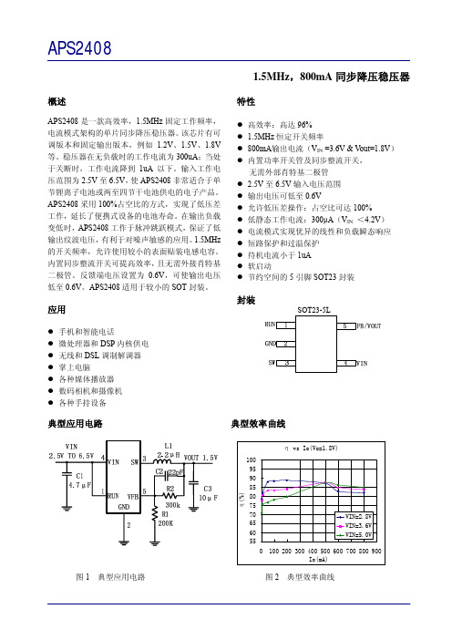
(注 2)
封装热阻
Ө ......................................................................................................................................................220°C/W
APS2408
1.5MHz,800mA 同步降压稳压器
概述
特性
APS2408 是一款高效率,1.5MHz 固定工作频率, 电流模式架构的单片同步降压稳压器。该芯片有可 调版本和固定输出版本,例如 1.2V、1.5V、1.8V 等。稳压器在无负载时的工作电流为 300uA;当处 于关断时,工作电流降到 1uA 以下。输入工作电 压范围为 2.5V 至 6.5V,使 APS2408 非常适合于单 节锂离子电池或两至四节干电池供电的电子产品。 APS2408 采用 100%占空比的方式,实现了低压差 工作,延长了便携式设备的电池寿命。在输出负载 变低时,APS2408 工作于脉冲跳跃模式,保证了低 输出纹波电压,有利于对噪声敏感的应用。1.5MHz 的开关频率,允许使用较小的表面贴装电感电容。 内置同步整流开关可提高效率,且无需外接肖特基 二极管。反馈端电压设置为 0.6V,可使输出电压 低至 0.6V。APS2408 适用于较小的 SOT 封装。
(注 4)
电气特性
(V =V = 3.6V, TA = 25°C, 除非另有说明) IN RUN
参数
条件
最小值 典型值
输入电压范围
2.5
输入 DC 供电电流 工作模式 停机模式
反馈电压
V 输入偏置电流
FB
基准电压线性调整率
DC/DC降压型转换器
户还可以导入 自己的数据 文件进行通 用 2 。G z P I 6 5 H X 综合测试仪
型研 究 ,从而 使得 整个 系统更 加 灵活 ,
能够满足 特殊用 户的测试需 求 。
Ke t l y ih e
一
NI BAE S se 与 y tms公 司 、P ae h s Mar ti 司 共 同 发 布 了一 款 针 对 军 事 和 x公
P ae Mar 公 司开发 的下变频模 VI 范 围内 。 h s ti x N
a s r a c o y t ms u t i mi r s s e
次探头 设 置连 接示波 器 ,即可 准确 地 、 块 ,包含射频 输入调 节模块 、微波频 段
确定性地 进行差分 测量 、单 端测量和 共 输入 、低频输 入 、本机振 荡器和 中频输
模测量 。
电 话 :0 - 7 2 5 0 5 6 6 —2 9 1 2
ht / www.utimirsse .o t / p: a sr coytmscm a
出调节模 块 。这五 个模块组 可设置成六 个 主 要 的 工 作 模 式 , 它 们 覆 盖 了
一
镯 : — 黔
应用的新型探头前端附件
的射频 /微波 下变频模块 为基础而 设计 用于单 节锂离子 电池或三节 AA 电池 的
这些 新型探头 前端附件 ,支持高 达 的 ,它拥 有从 1 0 Hz 6 5 0 k ~2 .GHz的频 应用 。 器件 支持 1 0 该 0 %的 占空 比 , 从而 8 Hz的信 号带 宽 ,是为探 测 D G DR2和 率 操 作 范 围 。 产 品 同 时 使 用 了 NI 司 可 实现 低 压 降 并从 电池 中汲 取 最 大 能 该 公
IP6510 原厂规格书

1/9 18319027317
VOUT CC1 CC2 DM DP
TYPEC
IP6510
22uH
L1
SW
3
C5 C4 R1
C3
10uF 220uF 2R 0.1uF
R2
BST
3.3
C6
4
K
1nF
CC1 7
IP6510 ESOP8
CC2 8
1 VOUT
VIN 2
DP 6
DM 5
C2 22uF
VIN 4.532V
IP6510
最大输出 18W,集成 Type-C PD 输出和各种快充输出协议 (DCP/QC2.0/QC3.0/FCP/AFC / USB PD)的 SOC IC
1 特性
同步开关降压转换器
内置功率 MOS 输入工作电压范围:4.5V 到 32V 输出电压范围:3V 到 12V,根据快充协
整机过温保护
ESD 4KV,直流耐压 48V
2 应用
车载充电器
快充适配器
智能排插
3 简介
IP6510 是一款集成同步开关的降压转换器、支 持 9 种输出快充协议、支持 Type-C 输出和 USB PD 协议,为车载充电器、快充适配器、智能排插 提供完整的解决方案。
IP6510 内置功率 MOS,输入电压范围是 4.5V 到 32V,输出电压范围是 3V 到 12V,能提供最 大 18W 的输出功率,能够根据识别到的快充协议自动调整
8 电气特性
除特别说明,TA=25℃,L=22uH,VIN=12v,Vout=5v
参数
符号
测试条件
输入系统 输入电压 输入欠压阈值
软开关同步升降压变换器的研究

软开关同步升降压变换器的研究0 引言提高开关频率可以减小电感、电容等储能元件的体积,但是开关频率的提高会增加开关器件的开关损耗。
为了解决这个问题,专家提出并发展了软开关技术。
一般来说,要实现比较理想的软开关效果,都需要有一个或-个以上的辅助开关为主开关创造软开关的条件。
同时希望辅助开关本身也能实现软开关。
升降压变换器作为一种最基本的DC/DC拓扑广泛应用于各种电源产品中。
由于升降压只包含一个开关,所以要实现软开关往往要附加很多有源或无源的额外电路,增加r变换器的成本,降低r变换器的可靠性。
升降压变换器除了有一个开关器件外还有一个二极管。
在较低压输出的场合,本身就希望用一个MOSPFET来替换二极管(同步整流),从而获得比较高的效率。
如果能利用这个同步开关作为主开关的辅助管,来创造软开关条件,同时本身又能实现软开关,那将是一个比较好的方案。
基于此,本文研究了一种软开关同步升降压变换器。
该方案适用于输出电压较低,功率密度较高的场合。
1 工作原理图1所示的是具有两个开关管的同步升降压变换器。
其两个开关互补导通,并设有一定的死区防止共态导通,。
通常设计中电感上的电流始终为一个方向,。
考虑到开关的结电容以及死区时间,一个周期可以分为5个阶段,各个阶段的等效电路。
下面简单介绍电感电流不改变方向情况下的同步升降压变换器的工作原理。
在这种情况下,S2可以实现软开关,但是S1只能工作在硬开关状态。
1)阶段1[to~t1]S1导通,L上承受输入电压,L上的电流线性增加。
在t1时刻,S1关断,该阶段结束。
2)阶段2[tl~t2] S1关断后,电感电流对S1的结电容进行充电,对S2的结电容进行放电,S2的漏源电压可以近似认为线性下降,直到下降到零,该阶段结束。
3)阶段3[t2~t3] 当S2的漏源电压下降到零之后,S2的寄生二极管就导通,将S2的漏源电压箝位在零电压状态,这也就为S2的零电压导通创造了条件。
4)阶段4[t3~t4] t3时刻S2的门极变为高电平,S2零电压开通。
降压型DC-DC转换器 XL7056 说明书

2.1A 100KHz 100V 降压型DC-DC转换器XL7056特点⏹最高输入电压100V⏹最大占空比85%⏹最小压差2.0V⏹输出电压从1.25V至20V可调⏹5V输出时最大2.1A输出电流⏹15V输出时最大1.2A输出电流⏹固定100KHz开关频率⏹最大输出功率小于20W⏹内置高压功率MOSFET⏹效率高达93%⏹出色的线性与负载调整率⏹内置限流功能⏹内置输出短路保护功能⏹TO263-7L封装应用⏹电动车控制器供电⏹通信描述XL7056是一款高效、高压降压型DC-DC转换器,固定100KHz开关频率,可提供最高2.1A输出电流能力,低纹波,出色的线性调整率与负载调整率。
XL7056内置固定频率振荡器与频率补偿电路,简化了电路设计。
PWM控制环路可以调节占空比从0~85%之间线性变化。
图1. XL7056封装2.1A 100KHz 100V 降压型DC-DC 转换器 XL7056引脚配置CSP CSN FB GNDSW 12345TO263-7LMetal Tab SWVC VIN 67图2. XL7056引脚配置表1.引脚说明引脚号 引脚名 描述 1 GND 接地引脚。
2 FB 反馈引脚,通过外部电阻分压网络,检测输出电压进行调整。
参考电压为1.25V 。
3 CSN 电流检测负端引脚。
4 SW 功率开关输出引脚。
5 CSP 电流检测正端引脚。
6 VC 内部电压调节器旁路电容引脚,需要在VIN 与VC 引脚之间连接1个1uF 电容。
7VIN电源输入引脚,需要在VIN 与GND 之间并联电容以消除噪声。
2.1A 100KHz 100V 降压型DC-DC 转换器 XL7056方框图EABias current & Voltage ReferenceVINGND75mV 1.25VEA COMPOscillator100KHz/25KHzSWRS Latch and DriverFBStart Up UVLOCSNSwitchVCocsCSP图3. XL7056方框图典型应用XL7056L1 100uH/3ACIN 100uF 100VC2105R210K 1%R13.3K 1%D1FSV10150SW FBGNDVINVIN7421CFF 10nF COUT 220uF 16VR30.035Ω 1%C1104VOUT 5V/0~2.1AOUTPUT 5V/0~2.1A VOUT=1.25*(1+R2/R1)CSP 53CSN CC 105VC6R3用于限制最大输出电流,当VOUT ≤5V 时,R3选择0.035欧姆;当VOUT>5V 时,R3选择0.055欧姆。
效率为96%的同步降压-升压型转换器
可支持电源管理总线( u ) P B 系统 编程开 关频率及高功率 密度 ,并有助于 M s 监控 保护及控制的l C
L 2 0 6 片 内 置 的 温 度 监 控 电路 M 56芯 缩 小 电路 板 尺 寸 。
善地 处理场 效应 管 ( 及混频 器偏 FET)
置 、通 道 检 测 和 控 制 ,为 增 加 的 LNB 功 能 提 供 了 一 个 稳 定 的 电源 。该 芯 片 可 为
多达4 个砷化镓 ( As或高 电子 流动 电 Ga ) 晶体场效应管( MT F T 提供偏置 , HE E )
口汇报 有关系统参数 和潜在故障 的最新
N5 0 2 C AS B 型、电感型及 电容 型负载的开 关 ,使设 情况 ,并且可 因应 各个故障事件设 置不 E 5 2 L S 要 求 ,并 顺 利 通 过 了 计 人 员 能 够 以 更 紧 凑 、 更 强 固 及 工 作 寿 同 的 警 告 阈 值 ,令 设 计 更 具 灵 活 性 ,也 赛宝专业测试 ,卓越的产 品性 能使它非 命 更 长 的 另一 选 择 ,替 代 机 电式 继 电器 令 系 统 受 到 较 全 面 的 保 护 。 或 分 立 电 路 。所 有 这 些 器 件 都 提 供 逻 辑 电平 输 入 。 常 适 用 于 电 压 波 动 较 大 ,对 电 磁 环 境 敏
满足EMl 设计要求的宽压输入D / c
D 模块电源 C
U RA LD 2 W 系 列 满 足 EM I 0
自保护低端M S E 驱动l OF T c
N CV8 0  ̄ 动 器 能 用 于 多 种 电 阻 4 x ̄
范 围之 外 。这 款 芯 片 可 以 通 过S B s M u 接
高压降压转换器LP6493车充芯片6496

高压降压转换器LP6493 车充芯片6496 高压降压转换器的主要功能是把一个较高的直流输入电压转换成较低的直流输出电压。
为了达到这个要求,MOSFET 以固定频率(fS),在脉宽调制信号(PWM)的控制下进行开、关操作。
当MOSFET 导通时,输入电压给电感和电容(L 和COUT)充电,通过它们把能量传递给负载。
LP6493、LP6496是一种高压降压转换器。
LP6493是一款500KHz固定频率同步电流模式高压降压转换器。
该器件集成了135mΩ高端开关和90mΩ低端开关,可在4.5V至28V的宽工作输入电压下提供3A的连续负载电流。
内部同步电源开关提高了效率,无需外部肖特基二极管。
电流模式控制提供快速的瞬态响应和循环电流限制。
在高负载下,LP6493工作在固定频率脉宽调制模式,具有出色的稳定性和瞬态响应。
在轻负载时,LP6493将以脉冲跳跃模式工作,以节省功耗.LP6493具有短路和热保护电路,以提高系统的可靠性。
外部可编程软启动允许在其他电源顺序上进行正确的上电,并避免启动期间的输入浪涌电流。
在关断模式下,电源电流降至1μA以下。
LP6493采用带裸焊盘的SOP-8封装。
应用分布式电源系统网络系统FPGA,DSP,ASIC电源特征轻负载时自动跳脉冲模式3A连续输出电流最小时间110ns集成的135mΩ高端开关集成90mΩ低端开关宽4.5V至28V工作输入范围输出可在0.8V至24V之间调整效率高达95%可编程软启动<1μA的关断电流500KHz固定开关频率热关断和过电流保护输入欠压锁定采用SOP-8(EP)封装符合RoHS标准和100%无铅(Pb)- 无卤LP6496是一款采用高压输入电源进行CC控制的同步降压型稳压器。
输入电压为8V〜40V时,LP6496具有良好的负载和线路稳定性,可实现5A的连续输出电流。
电流模式操作提供了快速的瞬态响应并简化了环路稳定性。
LP6496需要最少数量的易于使用的标准外部组件。
TLV62569P 2A 高效步进降压转换器数据手册说明书

V V L1TLV62569PProduct Folder Order Now Technical Documents Tools &SoftwareSupport &CommunityTLV62569,TLV62569PZHCSFR4C –DECEMBER 2016–REVISED OCTOBER 2017TLV62569采用SOT 封装的2A 高效同步降压转换器1特性•效率高达95%•低R DS(ON),可在100m Ω和60m Ω之间切换•输入电压范围:2.5V 至5.5V •可调输出电压:0.6V 至V IN •针对轻载效率的省电模式•针对最低压降的100%占空比•35µA 静态工作电流• 1.5MHz 典型开关频率•电源正常输出•过流保护•内部软启动•热关断保护•采用小外形尺寸晶体管(SOT)封装•与TLV62568引脚兼容•使用TLV62569并借助WEBENCH ®Power Designer 创建定制设计方案2应用•通用负载点(POL)电源•机顶盒•网络视频摄像头•无线路由器•硬盘3说明TLV62569器件是一款同步降压DC-DC 转换器,专门针对高效和紧凑型解决方案进行了优化。
该器件集成的开关能够提供高达2A 的输出电流。
在中等负载或重载条件下,该器件运行在脉宽调制(PWM)模式下,开关频率为1.5MHz 。
在轻载情况下,该器件自动进入节能模式(PSM),从而在整个负载电流范围内保持高效率。
关断时,流耗减少至2μA 以下。
TLV62569的输出电压可通过一个外部电阻分压器进行调节。
内部软启动电路可限制启动期间的浪涌电流。
此外,还内置了诸如输出过流保护、热关断保护和电源正常输出等其他特性。
该器件提供SOT23和SOT563两种封装。
器件信息(1)器件型号封装封装尺寸(标称值)TLV62569DBV SOT23(5) 2.90mm x 2.80mm TLV62569PDDC SOT23(6)TLV62569DRL SOT563(6) 1.60mm x 1.60mmTLV62569PDRLSOT563(6)(1)要了解所有可用封装,请参阅数据表末尾的可订购产品附录。