GC2365 CSP 模组设计指南_V1.03_20160224
发光二极管标准
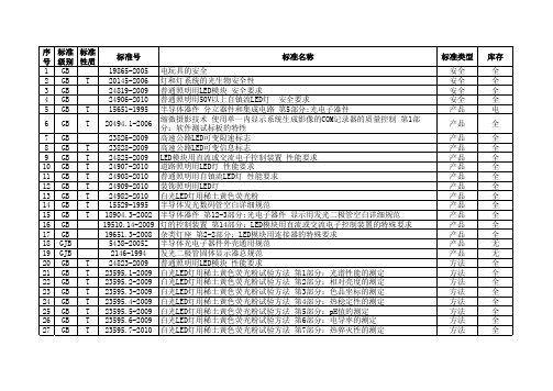
全 全 纸 纸 纸 全 电 纸 电 全 电 电 纸 电 纸5 26 27 28 29 30 31 32 33 34 35 36 37 38 39 40 41
SJ SJ SJ SJ SJ SJ SJ SJ SJ SJ JB SJ SJ SJ SJ SJ YS
T T T T
全 全 全
序 标准 标准 标准号 标准名称 号 级别 性质 1 YY 0055.2-2009 牙科-光固化机 第2部分:发光二极管(LED)灯 2 TY T 1001.1-2005 体育场馆设备使用要求及检验方法 第1部分:LED显示屏 3 SJ T 11396-2009 氮化镓基发光二极管用蓝宝石衬底片 4 SJ T 11397-2009 半导体发光二极管用荧光粉 5 SJ T 11401-2009 半导体发光二极管产品系列型谱 6 CJ T 229-2006 城市客车发光二级管显示屏 7 TB T 3085.2-2003 道客车车厢用灯 第二部分:卧铺车厢用LED床头阅读灯 8 CJ T 361-2011 水景用发光二极管(LED)灯 9 QB T 4146-2010 风光互补供电的LED道路和街路照明装置 10 GA T 484-2010 LED道路交通诱导可变信息标志 11 JT T 597-2004 LED车道控制标志 12 JT T 606.3-2004 高速公路监控设施通信规程 第3部分:LED可变信息标志 13 MT T 1092-2008 矿灯用LED及LED光源组技术条件 14 SJ T 11141-2003 LED 显示屏通用规范 15 SJ T 11393-2009 半导体光电子器件 功率发光二极管空白详细规范 16 SJ T 11398-2009 功率半导体发光二极管芯片技术规范 17 SJ T 11400-2009 半导体光电子器件 小功率发光二极管空白详细规范 18 SJ T 11406-2009 体育场馆用LED显示屏规范 19 SJ 20642/7-2000 半导体光电器件GR1325J型长波长发光二极管组件详细规范 20 TB T 3242-2010 LED铁路信号机构通用技术条件 21 QB T 4057-2010 普通照明用发光二极管 性能要求 22 SJ 50033.99-1995 半导体光电子器件GF511型橙/绿双色发光二极管详细规范 23 SJ 50033/136-1997 半导体光电子器件 GF116型红色发光二极管详细规范 24 SJ 50033/137-1997 半导体光电子器件 GF216型橙色发光二极管详细规范
基于FPGA的汽车尾灯系统硬件系统的设计

(作者单位:漯河技师学院)基于FPGA 的汽车尾灯系统硬件系统的设计赵娜◎一、硬件总体方案设计本系统采用FPGA EP2C5Q208C8N 核心板作为中央处理器,基本功能采用LED 显示不同情况,还具有红外接收报警功能、语音提示功能。
扩展部分由超声波测距功能、超声波报警功能。
根据要求通过按键设置手动操作,实现左转、右转、刹车、示宽、倒车语音提示及报警功能。
本系统主要由FPGA 核心模块、开关控制模块、显示模块、语音模块、红外收发报警模块、超声波测距报警模块六部分组成。
二、FPGA 核心模块1.开发板硬件资源介绍。
板载资源说明:AC2580_V3开发板设计了丰富的电路模块,基于此板用户可进行多种工程项目开发。
以下是对AC2580_V3开发板硬件资源的描述:(1)Altera Cyclone II EP2C5Q208C8N 或EP2C8Q208C8N 的FPGA 器件;(2)EPCS1(配EP2C5)或EPCS4(配EP2C8)串行配置器件;(3)16Mbytes SDRAM ,可为系统提供足够大的程序运行空间;(4)4Mbytes NOR FLASH ,符合CFI 规范,兼容4MB;(5)JTAG 和AS 双下载模式;(6)专用系统复位模块;(7)50MHZ 有源晶振(另预留一个晶振焊盘供扩展使用);(8)4个用户LED 指示灯;(9)4个用户按键;(10)2个80针扩展IO 接口;为了增加操作的灵活性AD2580_v3开发板上设计了一些跳线。
2.电源。
I/O 电压、内核电压供电连接,本核心板的所有I/O 脚都采用3.3V 电压标准,因此所有的VCC 、I /O 都连接3.3V ,VCCINT 为FPGA 内核工作电压输入,CycloneII 系列的FPGA 均采用1.2V 的内核电压,所以这里连接1.2V 。
3.时钟源。
无论是用离散逻辑、可编程逻辑,还是基于其他类型器件的任何数字设计,系统的成功运行都要依靠可靠的时钟。
AE-2M-3005 GC2375 CSP 模组设计指南 V1.0_20160520
GENERATION REVISION HISTORYREV. EFFECTIVEDATEDESCRIPTION OF CHANGESPREPARED BY1.0 2016-05-20 Document Release AE Dept.GCC on fi d e n ti al目录1. 外围电路 (4)2. 设计说明 (4)3. GC2375 CSP封装说明 (6)3.1 Optical Center (unit: µm) (6)3.2 GC2375 CSP封装(单位:µm) (7)3.3 CSP封装点阵表 (7)3.4 CSP封装管脚说明 (8)3.5 PCB焊盘设计说明示意图(单位:µm) (9)3.6模组成像方向 (9)3.7 CSP封装尺寸图(单位:μm) (10)3.8 CSP 封装说明 (11)G C C on fi d en ti a l1. 外围电路MIPI 1 lane图1-1 MIPI 接口外围电路图2. 设计说明外围电路设计说明◆ GC2375芯片分三路电源:AVDD28、DVDD18、IOVDD 。
AVDD28为模拟供电电源,2.7~3.0V ;DVDD18为数字电路供电电源,1.7~1.9V ; IOVDD 为I/O 电源,1.7~3.0V ;◆ 靠近电源处,加如图示滤波电容,容值请参照外围电路图;注意:A VDD 上电容(C4)规格为C0402;◆ 电容摆放应尽量靠近电源Pin 脚;◆ 所有电容均不可省去,否则会影响图像质量;◆ AGND 、DGND 需要在FPC 上靠近芯片端接到一起,铺地后引出到连接器端,否则会影响图像质量;◆ GND 走线尽量要粗,至少加粗至0.2mm 以上,尽量多打一些过孔; ◆ 电源线走线宽度至少加粗至0.2mm 以上; ◆ 芯片有RESET pin ,需要引出控制;◆ FPC/PCB 布线时尽量让SBDA/SBCL 线远离高速的信号线;◆ MCP 、MCN 需要尽量平行走线,等长;尽量少打或不打过孔;且要远离高GCC on fi d ti al频信号线(如MCLK),最好是能用地线保护起来,且差分线对走线的背面也尽量是地线走线,并铺地铜作为参考层。
SC1035设计应用指南_v1p5
1280X960@30fps 的寄存器配置。
1,更新表 2-5 中 PLL 配置寄存器的说明。
Bill,20140927
2, 在表 2-3 和表 2-4 中增加了每种配置条件下的输出 pixel
clock frequency。
3,表 2-2 中$3631 寄存器的配置值从$84 改为$80。
4,在 2.4 节中增加对 BLC 和 RNC target 值的使用说明。
2 寄存器基本配置 ......................................................................................... 11
2.1 设备地址............................................................................................................. 11 2.2 正常工作时的基本配置..................................................................................... 11 2.3 PLL 配置说明 ....................................................................................................15 2.4 RNC 和 BLC.......................................................................................................16
威莱恩 模型8635CU 内饰灯说明书

©2001 Whelen Engineering Company Inc. Form No. 13013J (122017)Model 8635CU Interior LightInstallation:1.Be sure that the selected mounting area does not hide anything that could be damagedby cutting the interior light’s mounting hole.ing the supplied dimensions,cut the mounting hole for your light.Follow thedimensions exactly as shown.3.Feed the lamp assembly wires through the hole in the reflector as shown in Fig.1.TheWHITE wire is ground(-),the BLACK wire is for high power operation(35watts)12 VDC,and the RED wire is for low power operation(14watts)e appropriate wire connectors.All customer supplied wires that connect to the positive terminal of the battery must be sized to supply at least125%of the maximum operating current and FUSED at the battery to carry that load.DO NOT USE CIRCUIT BREAKERS WITH THIS PRODUCT!4.Insert lamp assembly into reflector housing.Be sure assembly is fully seated intohousing.Lock the lamp assembly in place by rotating1/8turn in a clockwise direction.5.Insert reflector/lamp unit into the mounting hole.Be sure no wires are caught betweenmounting surface and reflector/lamp unit.6.Hold the reflector/lamp unit firmly against the mounting surface and insert a reflectorclamp through the reflector(Fig.2).7.Insert the two mounting screws and tighten with a Phillips screwdriver.This willsqueeze the mounting surface between the clamp and the reflector.Repeat procedure for the remaining clamp.8.Now the interior light’s lens may be installed as shown in Fig3.The lens must bealigned as shown and simply snaps into place.Do not allow insulation of any kind to cover the back of the lighthead.The resulting heat will damage the lighthead and could cause a fire!Reflector/LampUnitLensFIG. 3Surface SurfaceScrewSafety First: This document provides all the necessary information to allow your Whelen product to be properly and safely installed. Before beginning the installation and/or operation of your new product, the installation technician and operator must read this manual completely. Important information is contained herein that could prevent serious injury or damage.•Proper installation of this product requires the installer to have a good understanding of automotive electronics,systems and procedures.•Whelen Engineering requires the use of waterproof butt splices and/or connectors if that connector could be exposed to moisture.•Any holes,either created or utilized by this product,should be made both air-and watertight using a sealant recommended by your vehicle manufacturer.•Failure to use specified installation parts and/or hardware will void the product warranty!•If mounting this product requires drilling holes,the installer MUST be sure that no vehicle components or other vital parts could be damaged by the drilling process.Check both sides of the mounting surface before drilling begins.Also de-burr any holes and remove any metal shards or remnants.Install grommets into all wire passage holes.•Do not install this product or route any wires in the deployment area of your air bag.Equipment mounted or located in the air bag deployment area will damage or reduce the effectiveness of the air bag,or become a projectile that could cause serious personal injury or death.Refer to your vehicle owner's manual for the air bag deployment area.The User/Installer assumes full responsibility to determine proper mounting location,based on providing ultimate safety to all passengers inside the vehicle.•For this product to operate at optimum efficiency,a good electrical connection to chassis ground must be made.The recommended procedure requires the product ground wire to be connected directly to the NEGATIVE(-)battery post.•If this product uses a remote device to activate or control this product,make sure that this control is located in an area that allows both the vehicle and the control to be operated safely in any driving condition.•Do not attempt to activate or control this device in a hazardous driving situation.•This product contains either strobe light(s),halogen light(s),high-intensity LEDs or a combination of these lights.Do not stare directly into these lights.Momentary blindness and/or eye damage could result.•Use only soap and water to clean the outer e of other chemicals could result in premature lens cracking(crazing)and discoloration.Lenses in this condition have significantly reduced effectiveness and should be replaced immediately.Inspect and operate this product regularly to confirm its proper operation and mounting condition.Do not use a pressure washer to clean this product.•WARNING!All customer supplied wires that connect to the positive(+) terminal of the battery must be sized to supply at least125%of the maximum operating current and“at the battery”to carry that load.DO NOT USEFUSEDCIRCUIT BREAKERS WITH THIS PRODUCT!•FAILURE TO FOLLOW THESE PRECAUTIONS AND INSTRUCTIONS COULD RESULT IN DAMAGE TO THE PRODUCT OR VEHICLE AND/OR SERIOUS INJURY TO YOU AND YOUR PASSENGERS!®ENGINEERING COMPANY INC.51 Winthrop RoadChester, Connecticut 06412-0684Phone: (860) 526-9504SalesEmail:*******************CanadianSales:************************CustomerService:*******************For warranty information regarding this product, visit /warrantyWarnings to InstallersWhelen’s emergency vehicle warning devices must be properly mounted and wired in order to be effective and safe. Read and follow all of Whelen’s written instructions when installing or using this device. Emergency vehicles are often operated under high speed stressful conditions which must be accounted for when installing all emergency warning devices. Controls should be placed within convenient reach of the operator so that he can operate the system without taking his eyes off the roadway. Emergency warning devices can require high electrical voltages and/or currents. Properly protect and use caution around live electrical connections.Grounding or shorting of electrical connections can cause high current arcing, which can cause personal injury and/or vehicle damage, including fire. Many electronic devices used in emergency vehicles can create or be affected by electromagnetic interference.Therefore, after installation of any electronic device it is necessary to test all electronic equipment simultaneously to insure that they operate free of interference from other components within the vehicle. Never power emergency warning equipment from the same circuit or share the same grounding circuit with radio communication equipment.All devices should be mounted in accordance with the manufacturer’s instructions and securely fastened to vehicle elements of sufficient strength to withstand the forces applied to the device. Driver and/or passenger air bags (SRS) will affect the way equipment should be mounted.This device should be mounted by permanent installation and within the zones specified by the vehicle manufacturer, if any.Any device mounted in the deployment area of an air bag will damage or reduce the effectiveness of the air bag and may damage or dislodge the device. Installer must be sure that this device, its mounting hardware and electrical supply wiring does not interfere with the air bag or the SRS wiring or sensors. Mounting the unit inside the vehicle by a method other than permanent installation is not recommended as unit may become dislodged during swerving; sudden braking or collision. Failure to follow instructions can result in personal injury. Whelen assumes no liability for any loss resulting from the use of this warning device. PROPER INSTALLATION COMBINED WITH OPERATOR TRAINING IN THE PROPER USE OF EMERGENCY WARNING DEVICES IS ESSENTIAL TO INSURE THE SAFETY OF EMERGENCY PERSONNEL AND THE PUBLIC.Warnings to UsersWhelen’s emergency vehicle warning devices are intended to alert other operators and pedestrians to the presence and operation of emergency vehicles and personnel. However, the use of this or any other Whelen emergency warning device does not guarantee that you will have the right-of-way or that other drivers and pedestrians will properly heed an emergency warning signal. Never assume you have the right-of-way. It is your responsibility to proceed safely before entering an intersection, driving against traffic, responding at a high rate of speed, or walking on or around traffic lanes. Emergency vehicle warning devices should be tested on a daily basis to ensure that they operate properly. When in actual use, the operator must ensure that both visual and audible warnings are not blocked by vehicle components (i.e.: open trunks or compartment doors), people, vehicles, or other obstructions. It is the user’s responsibility to understand and obey all laws regarding emergency warning devices.The user should be familiar with all applicable laws and regulations prior to the use of any emergency vehicle warning device. Whelen’s audible warning devices are designed to project sound in a forward direction away from the vehicle occupants. However, because sustained periodic exposure to loud sounds can cause hearing loss, all audible warning devices should be installed and operated in accordance with the standards established by the National Fire Protection Association.。
RAE Systems by Honeywell 应用指南AP-236说明书

Certain professions have higher risk of exposure due to constant contact with automobile fumes these being truck drivers, police, and conductors of urban buses. Although the base risk is the same as other people these types of professions have repeated daily exposure throughout their careers. The actual risk by measurement of the atmospheric readings of the European Counsel and the National Board of Health and Welfare is on the order of 10mcg/m3 of atmosphere or less, this being overall a low risk (INRS).
• Petroleum refining (Oil refineries) • Coke and Coal manufacturing • Rubber tire manufacturing • Storage sites (tank farms) • Transportation services (ships, tanker trucks) • Laboratories • Chemical manufacturing
In addition to triggering cancer, exposure to this compound at high concentrations in the 10,000 to 20,000 ppm range will result in death. Finally, Benzene is a suspected toxicant to numerous systems critical to life. To include:
1.2365热处理工艺文档
1.2365热处理工艺热处理是一种常用的金属材料加工技术,通过控制材料的加热温度和冷却速度,改变材料的力学性能和组织结构。
本文将详细介绍1.2365热处理工艺,包括其特性、用途、步骤以及注意事项。
1.2365工具钢是一种具有高硬度和优异耐热性能的工具钢。
它具有良好的耐磨性和切削性能,广泛应用于模具、刀具和冲压模等领域。
1.2365热处理工艺通过控制材料的金相组织,优化其力学性能,提高工具的使用寿命。
1.2365热处理工艺主要用于提高工具钢的硬度和耐磨性能,以满足工具在严苛工作环境下的需求。
该工艺适用于各类切削工具、模具和冲压模等需要高硬度和耐磨性的工作场景。
1. 预处理:将1.2365工具钢材料浸泡于盐酸或硝酸等溶液中进行脱脂处理,去除表面的油污和杂质,确保材料表面清洁。
2. 加热:将经过预处理的1.2365工具钢材料放入炉内,控制加热温度并保持一定时间,使材料达到适当的热处理温度。
3. 保温:在达到适当加热温度后,使材料保持一定时间(一般为几十分钟至数小时),以保证材料内部的温度均匀分布,实现组织结构的改变。
4. 冷却:将保温后的1.2365工具钢材料迅速冷却到室温。
冷却速度的控制对于材料的组织结构和性能具有重要影响。
5. 回火:在冷却之后,将材料再次加热至适当的温度,并进行适当的保温和冷却,以减轻材料内部的应力,提高韧性和强度。
四、1.2365热处理工艺的注意事项1. 加热温度的选择要根据具体应用场景进行,过高的温度可能导致材料晶粒长大或丧失硬度。
2. 保温时间的选择要根据工艺图和试验结果进行,过短的时间无法充分改变材料的组织结构,过长的时间可能产生不良影响。
3. 冷却速度的选择要根据材料的要求进行。
油冷、水冷和空冷是常用的冷却方法,冷却速度过快可能导致开裂或变形。
4. 回火工艺要根据具体材料和性能需求进行,过高或过低的温度都可能影响材料的性能。
通过对1.2365热处理工艺的详细介绍,我们了解到该工艺主要用于提高工具钢的硬度和耐磨性能。
一种基于CSP封装结构的侧入式面板灯及背光模组[实用新型专利]
![一种基于CSP封装结构的侧入式面板灯及背光模组[实用新型专利]](https://img.taocdn.com/s3/m/0cb718a7767f5acfa0c7cd8f.png)
专利名称:一种基于CSP封装结构的侧入式面板灯及背光模组专利类型:实用新型专利
发明人:杨梅刚,熊毅,朱富斌,王跃飞
申请号:CN201520904006.1
申请日:20151113
公开号:CN205137105U
公开日:
20160406
专利内容由知识产权出版社提供
摘要:本实用新型公开了一种基于CSP封装结构的侧入式面板灯及背光模组。
基于CSP封装结构的侧入式面板灯,包括壳体、灯条和导光板,壳体的至少一内侧壁上安装有灯条,导光板设在壳体内,导光板的侧面对着灯条;所述的灯条包括基板,在基板上设有二个以上的三面出光的CSP封装结构,三面出光的CSP封装结构包括倒装晶片;倒装晶片的两相对侧面封装有挡光胶,倒装晶片的另外两相对侧面和顶面上封装有封装胶。
基于CSP封装结构的背光模组,包括壳体、灯条、导光板和扩散板,壳体的至少一内侧壁上安装有灯条,导光板设在壳体内,导光板的侧面对着灯条,扩散板位于导光板的前方。
本实用新型的结构能提高光的利用率,减小暗区,提高出光的均匀性。
申请人:广州市鸿利光电股份有限公司
地址:510890 广东省广州市花都区花东镇先科一路1号
国籍:CN
代理机构:广州中浚雄杰知识产权代理有限责任公司
代理人:刘各慧
更多信息请下载全文后查看。
236安装手册资料
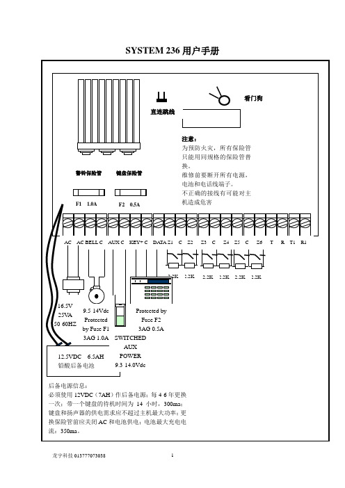
SYSTEM 236用户手册图中文字说明:警告:为防止火灾发生,更换保险管时要使用相同规格和容量的保险管。
更换前要断开交流电、电池和电话线。
注意:警铃(BELL)、附设电源(AUX)和键盘(KEY+)端口的总工作电流不能超过800mA。
其中AUX和KEY端工作电流不能超过400mA。
电话线缆9.APGF红线——电话进线(R)绿线——电话进线(T)灰线——电话机(R1)棕线——电话机(T1)兰线——防拆橙线——防拆注意事项机箱门合页处要用16AWG,绿色实芯导线连接地线。
所有输出都受到电流功率限制。
*如果编程为线尾阻回路(EOL)或监控回路,则2.2KΩ电阻必须接在回路的尾端。
*回路电压:0.00——1.50VDC=短路1.60——3.10VDC=正常3.20——5.00VDC=开路*图中标为黑圆的接线端为电路公共端。
*当作为火警系统使用时,应用4线式烟感探测器(SYSTEM2412)在电源回路的末端配有电源监控EOL继电器组件(A77-716系列)。
电源要求*只能使用12VDC,6.5Ah密封铅酸电池。
*每4-6年更新电池C&K1265型。
*配用一台键盘,在300mA耗电时,备用电池工作14小时。
*附设电源,键盘和发声器和发声器的电功率不能超过最大容量。
*在无开关控制的电源插座上装C&k1097-B电源变压器。
*电池最大充电电流=56mA注:本图中所有标出的容限值均符合UL985,UL1023,和UL1635标准。
目录System 236端口标准UL标准安装主机接线开机配置键盘设置键盘地址厂家预置状态编程选项(按英文字母顺序列表)主机编程用LED键盘编程用字母键盘编程输入十六进制数字母键盘编程编辑字母和数字特殊功能键编程选择(按数字顺序)电话线路问题“看门狗”指示键盘操作指令表常见问题处理减少误报注意事项编程工作表本手册所介绍的是SYSTEM236控制/通信器的安装与编程方法,有关遥控编程的内容请见指挥者Ⅱ/监测察Ⅱ者软件用户手册。
DSA2361 备自投使用手册
DSA2361/2362/2363/2364/2365备自投装置使用说明书(V2.00)编写:仇新宏校对:黄宏青审核:顾欣欣批准:季侃DSA2361/2362/2363/2364/2365备自投装置使用说明书1 人机界面及操作 (3)1.1指示灯 (4)1.2键盘使用 (4)1.3装置前置板说明 (5)1.4屏保界面 (6)2 菜单操作 (7)2.1交直流量测量值 (9)2.2信息记录查询 (11)2.2.1 单元信息记录 (11)2.2.2保护事件记录 (12)2.2.3遥信事件记录 (12)2.2.4自检事件记录 (13)2.2.5单元事件记录 (13)2.2.6录波事件记录 (13)2.2.7电流越限记录 (14)2.3单元定值整定 (14)2.3.1通讯整定 (14)2.3.2保护转遥信投退 (15)2.3.3 变化遥测投退 (16)2.3.4日期及时间整定 (16)2.3.5口令投退 (16)2.3.6 控制回路断线投退 (17)2.3.7 开关偷跳启动事故总投退 (17)2.3.8 液晶背光常亮投退 (18)2.3.9 保护信号远方测试 (18)2.4保护定值投退 (18)2.5保护定值整定 (19)2.6测量定值整定 (20)2.6.1遥控脉宽定值 (20)2.6.2遥信整定 (20)2.7交流量精度调节 (21)2.8信号复归 (21)2.9系统复归 (22)3 用户调试大纲 (22)3.1通电前 (22)3.2通电后检查 (22)3.3采样精度检查 (22)3.4节点输出校验 (23)3.5定值校验 (23)4 维护说明 (23)5 背板端子 (24)南瑞城乡电网公司 1DSA2361/2362/2363/2364/2365备自投装置使用说明书5.1采样板 (24)5.2POW ER板 (25)5.3IO B板 (25)5.4OPA操作板 (27)附录 (27)附录1遥信表 (27)附录2装置菜单列表 (31)南瑞城乡电网公司 2DSA2361/2362/2363/2364/2365备自投装置使用说明书DSA236X备自投系列保护装置,根据现场不同的运行情况分为5种不同型号,分别是:DSA2361、DSA2362、DSA2363、DSA2364、DSA2365。
LTC2365资料
123656fFEATURESAPPLICATIONSDESCRIPTIONSampling ADCs in TSOTThe L TC ®2365/L TC2366 are 1Msps/3Msps, 12-bit, sam-pling A/D converters that draw only 2mA and 2.6mA, re-spectively, from a single 3V supply. These high performance devices include a high dynamic range sample-and-hold and a high speed serial interface. The full scale input is 0V to V DD or V REF . Outstanding AC performance includes 72dB SINAD and –80dB THD at sample rates of 3Msps. The serial interface provides fl exible power management and allows maximum power effi ciency at low throughput rates. These devices are available in tiny 6- and 8-lead TSOT-23 packages.The serial interface, tiny TSOT-23 package and extremely high s ample r ate-to-power r atio m ake t he L TC2365/L TC2366 ideal for compact, low power , high speed systems.The high impedance single-ended analog input and the ability to operate with reduced spans (down to 1.4V full scale) allow direct connection to sensors and transducers in many applications, eliminating the need for gain stages.Single 3V Supply, 3Msps, 12-Bit Sampling ADCn12-Bit Resolutionn 1Msps/3Msps Sampling Rates n Low Noise: 73dB SNRn Low Power Dissipation: 6mWn Single Supply 2.35V to 3.6V Operation n No Data Latencyn Sleep Mode with 0.1μA Typical Supply Current n Dedicated External Reference (TSOT23-8)n 1V to 3.6V Digital Output Supply (TSOT23-8)n SPI/MICROWIRE ™ Compatible Serial I/O n Guaranteed Operation from –40°C to 125°C n 6- and 8-Lead TSOT-23 PackagesnCommunication Systems n Data Acquisition Systems n Handheld Terminal Interface n Medical Imagingn Uninterrupted Power Supplies n Battery Operated Systems n Automotive1MHz Sine Wave 8192 FFT Plot12-Bit TSOT23-6/-8 ADC FamilyDATA OUTPUT RATE 3Msps 1Msps 500ksps 250ksps 100ksps Part NumberL TC2366L TC2365L TC2362L TC2361L TC2360T YPICAL APPLICATION L , L T , L TC and L TM are registered trademarks of Linear Technology Corporation. All other trademarks are the property of their respective owners. Protected by U.S.SERIAL DATA LINK TO ASIC, PLD, MPU, DSP OR SHIFT REGISTERS DIGITAL OUTPUT SUPPLY 1V TO 3.6VINPUT FREQUENCY (kHz)00–20–40–60–80–100–120–140750125023656 TA01b25050010001500M A G N I T U E (d B )V DD = 3Vf SMPL = 3Msps f IN= 994kHzSINAD = 72dB THD = –80.3dB223656fABSOLUTE MAXIMUM RATINGSSupply Voltage (V DD , OV DD ) .....................................4.0V V REF and Analog Input Voltage (Note 3) .........................................–0.3V to (V DD + 0.3V)Digital Input Voltage ......................–0.3V to (V DD + 0.3V)Digital Output Voltage ...................–0.3V to (V DD + 0.3V)Power Dissipation ...............................................100mW(Notes 1, 2)Lead Free FinishTAPE AND REEL (MINI)TAPE AND REEL PART MARKING*PACKAGE DESCRIPTION TEMPERATURE RANGE L TC2366CTS8#TRMPBF L TC2366CTS8#TRPBF L TCYZ 8-lead Plastic TSOT-230°C to 70°C L TC2366ITS8#TRMPBF L TC2366ITS8#TRPBF L TCYZ 8-lead Plastic TSOT-23–40°C to 85°C L TC2366HTS8#TRMPBF L TC2366HTS8#TRPBF L TCYZ 8-lead Plastic TSOT-23–40°C to 125°C L TC2366CS6#TRMPBF L TC2366CS6#TRPBF L TCXK 6-lead Plastic TSOT-230°C to 70°C L TC2366IS6#TRMPBF L TC2366IS6#TRPBF L TCXK 6-lead Plastic TSOT-23–40°C to 85°C L TC2366HS6#TRMPBF L TC2366HS6#TRPBF L TCXK 6-lead Plastic TSOT-23–40°C to 125°C L TC2365CTS8#TRMPBF L TC2365CTS8#TRPBF L TDCB 8-lead Plastic TSOT-230°C to 70°C L TC2365ITS8#TRMPBF L TC2365ITS8#TRPBF L TDCB 8-lead Plastic TSOT-23–40°C to 85°C L TC2365HTS8#TRMPBF L TC2365HTS8#TRPBF L TDCB 8-lead Plastic TSOT-23–40°C to 125°C L TC2365CS6#TRMPBF L TC2365CS6#TRPBF L TDCC 6-lead Plastic TSOT-230°C to 70°C L TC2365IS6#TRMPBF L TC2365IS6#TRPBF L TDCC 6-lead Plastic TSOT-23–40°C to 85°C L TC2365HS6#TRMPBFL TC2365HS6#TRPBFL TDCC6-lead Plastic TSOT-23–40°C to 125°CTRM = 500 pieces. *Temperature grades are identifi ed by a label on the shipping container .Consult L TC Marketing for information on lead based fi nish parts.For more information on lead free part marking, go to: http://www.linear .com/leadfree/For more information on tape and reel specifi cations, go to: http://www.linear .com/tapeandreel/Operating Temperature RangeL TC2365C/L TC2366C ...............................0°C to 70°C L TC2365I/L TC2366I ..............................–40°C to 85°C L TC2365H/L TC2366H (Note 13) .........–40°C to 125°C Storage Temperature Range ...................–65°C to 150°C Lead Temperature (Soldering, 10 sec) ..................300°CORDER INFORMATIONPIN CONFIGURATIONThel denotes the specifi cations which apply over the full operating temperature range, otherwise specifi cations are at T A = 25°C. (Note 4)CONVERTER CHARACTERISTICSPARAMETER CONDITIONSL TC2365L TC2366UNITS MIN TYP MAX MIN TYP MAXResolution (No Missing Codes)l1212Bits Integral Linearity Error(Note 5, 6)l±0.25±1±0.25±1LSB Differential Linearity Error(Note 6)l±0.25±1±0.25±1LSB T ransition Noise(Note 7)0.340.34LSB RMS Offset Error(Note 6)l2±3.52±3.5LSB Gain Error(Note 6)l1±21±2LSBTotal Unadjusted Error S6 Package (Note 6)TS8 Package (Note 6)ll23±3.5±4.523±3.5±4.5LSBLSBThel denotes the specifi cations which apply over the full operating temperature range, otherwise specifi cations are at T A = 25°C. (Note 4)ANALOG INPUTSSYMBOL PARAMETER CONDITIONS MIN TYP MAX UNITSV IN Analog Input Voltage S6 PackageTS8 Package ll–0.05–0.05V DD + 0.05V REF + 0.05VVI IN Analog Input Leakage Current CS = High l±1μAC IN Analog Input Capacitance Between ConversionsDuring Conversions 204pFpFV REF Reference Input Voltage TS8 Package l 1.4V DD + 0.05V I REF Reference Input Leakage Current TS8 Package l±1μA C REF Reference Input Capacitance TS8 Package4pF t AP Sample-and-Hold Aperture Delay Time1ns t JITTER Sample-and-Hold Aperture Delay Time Jitter0.3nsDYNAMIC ACCURACYThel denotes the specifi cations which apply over the full operating temperature range, otherwise specifi cations are at T A = 25°C. (Note 4)SYMBOL PARAMETER CONDITIONSL TC2365L TC2366UNITS MIN TYP MAX MIN TYP MAXSINAD Signal-to-(Noise + Distortion) Ratio f IN = 1MHz l68726871dB SNR Signal-to-Noise Ratio f IN = 1MHz l70736972dB THD Total Harmonic Distortion f IN = 1MHz l–86–72–80–72dB SFDR Spurious Free Dynamic Range f IN = 1MHz8782IMD Intermodulation Distortion f IN1 = 0.97MHz, f IN2 = 1MHz for L TC2366f IN1 = 97kHz, f IN2 = 100kHz for L TC2365–76–71.5dBFull Power Bandwidth At 3dBAt 0.1dB 305508MHzMHzFull Linear Bandwidth SINAD ≥ 68dB2 2.5MHz323656fThel denotes the specifi cations which apply over the fulloperating temperature range, otherwise specifi cations are at T A = 25°C. (Note 4)DIGITAL INPUTS AND DIGITAL OUTPUTSSYMBOL PARAMETER CONDITIONS MIN TYP MAX UNITSV IH High Level Input Voltage 2.7V < V DD ≤ 3.6V2.35V ≤ V DD ≤ 2.7V ll21.7VVV IL Low Level Input Voltage 2.7V < V DD ≤ 3.6V2.35V ≤ V DD ≤ 2.7V ll0.80.7VVI IH High Level Input Current V IN = V DD l 2.5μA I IL Low Level Input Current V IN = 0V l–2.5μA C IN Digital Input Capacitance2pF V OH High Level Output Voltage V DD = 2.35V to 3.6V, I SOURCE = 200μA l V DD –0.2V V OL Low Level Output Voltage V DD = 2.35V to 3.6V, I SINK = 200μA l0.2V I OZ Hi-Z Output Leakage CS = V DD l±3μA C OZ Hi-Z Output Capacitance CS = V DD4pF I SOURCE Output Source Current V OUT = 0V–10mA I SINK Output Sink Current V OUT = V DD10mAPOWER REQUIREMENTSYMBOL PARAMETER CONDITIONS MIN TYP MAX UNITS V DD Supply Voltage l 2.35 3.0 3.6V O VDD Digital Output Supply Voltage l1 3.6VI DD Supply Current, Static ModeOperational Mode, L TC2366Operational Mode, L TC2365Sleep ModeSleep Mode CS = 0V, SCK = 0V or V DDf SMPL = 3Mspsf SMPL = 1Msps–40°C to +85°C+85°C to +125°Cllll12.620.143.525mAmAmAμAμAP D Power Dissipation, Static ModeOperational Mode, L TC2366Operational Mode, L TC2365Sleep ModeSleep Mode CS = 0V, SCK = 0V or V DDf SMPL = 3Mspsf SMPL = 1Msps–40°C to +85°C+85°C to +125°Cllll7.860.33.614.412.67.218mWmWmWμWμW423656f523656fNote 1: Stresses beyond those listed under Absolute Maximum Ratings may cause permanent damage to the device. Exposure to any Absolute Maximum Rating condition for extended periods may affect device reliability and lifetime.Note 2: All voltage values are with respect to GND.Note 3: When this pin, A IN , is taken below GND or above V DD , it will be clamped by internal diodes. These products can handle input currents greater than 100mA below GND or above V DD without latchup.Note 4: V DD = OV DD = V REF = 2.35V to 3.6V , f SMPL = f SMPL(MAX) and f SCK =f SCK(MAX) unless otherwise specified.Note 5: Integral linearity is defi ned as the deviation of a code from astraight line passing through the actual endpoints of the transfer curve. The deviation is measured from the center of the quantization band.Note 6: Linearity, offset and gain specifi cations apply for a single-ended A IN input with respect to GND.Note 7: Typical RMS noise at code transitions.Note 8: Guaranteed by characterization. All input signals are specifi ed with t r = t f = 2ns (10% to 90% of V DD ) and timed from a voltage level of 1.6V .Note 9: All timing specifi cations given are with a 10pF capacitance load. With a capacitance load greater than this value, a digital buffer or latch must be used.Note 10: Minimum f SCK at which specifications are guaranteed.Note 11: The time required for the output to cross the V IH or V IL voltage. Note 12: Guaranteed by design, not subject to test.Note 13: High temperatures degrade operating lifetimes. Operating lifetime is derated at temperatures greater than 105°C.SYMBOL PARAMETERCONDITIONS L TC2365L TC2366UNITSMIN TYPMAX MIN TYPMAX f SMPL(MAX)Maximum Sampling Frequency (Notes 8, 9)l 13MHz f SCK Shift Clock Frequency (Notes 8, 9, 10)l 0.5160.548MHz t SCK Shift Clock Periodl 62.5200020.82000ns t THROUGHPUT Minimum Throughput Time, t ACQ + t CONV l 1000333ns t ACQ Acquisition Time l 181.556ns t CONV Conversion Time l 818.5277ns t QUIET SDO Hi-Z State to CS ↓(Notes 8, 9)l 44ns t 1Minimum Positive or Negative CS Pulse Width (Notes 8)l 44ns t 2SCK ↓ Setup Time After CS ↓ (Notes 8)l 6200062000ns t 3SDO Enabled Time After CS ↓(Notes 9, 11, 12)l 44ns t 4SDO Data Valid Access Time After SCK ↓ (Notes 8, 9, 11)l 1515ns t 5SCK Low Time l 40%40%t SCK t 6SCK High Timel 40%40%t SCK t 7SDO Data Valid Hold Time After SCK ↓ (Notes 8, 9, 11)l 55ns t 8SDO Into Hi-Z State Time After SCK ↓(Notes 9, 12)l 530514ns t 9SDO Into Hi-Z State Time After CS ↑(Notes 9, 12)l 4.2 4.2ns t POWER-UPPower-up Time from Sleep ModeSee Sleep Mode section l1000333nsTIMING CHARACTERISTICSThe l denotes the specifi cations which apply over the full operating temperature range, otherwise specifi cations are at T A = 25°C. (Note 4)623656fT A = 25°C, V DD = OV DD = V REF (L TC2365, Note 4)TYPICAL PERFORMANCE CHARACTERISTICSIntegral Nonlinearity vs Output CodeDifferential Nonlinearity vs Output CodeIntegral and DifferentialNonlinearity vs Supply VoltageHistogram for 16384 ConversionsSNR vs Input FrequencySINAD vs Input FrequencyTHD vs Input FrequencyTHD vs Input Resistance461kHz Sine Wave 8192 FFT PlotOUTPUT CODE–1.0I N L (L S B )–0.8–0.4–0.201.00.41024204823656 G01–0.60.60.80.230724096V DD = 3V OUTPUT CODE–1.0D N L (L S B )–0.8–0.4–0.201.00.41024204823656 G02–0.60.60.80.230724096V DD = 3VSUPPL Y VOL TAGE (V)2.1I N L A N D D N L (L S B )0.20.61.0 3.323656 G03–0.2–0.600.40.8–0.4–0.8–1.02.42.73.0 3.6CODE20450C O U N T200040006000800010000204620472048204923656 G042050INPUT FREQUENCY (kHz)100S N R (d B )72.973.123656 G0572.772.5100073.573.3INPUT FREQUENCY (kHz)10072.0S I N A D (d B )72.272.472.672.873.073.2100023656 G06INPUT FREQUENCY (kHz)100–84–83–8123656 G07–85–861000–87–88–82T H D (d B )INPUT RESISTANCE (Ω)T H D (d B )–81–8010023656 G08–82–83255075–78–79INPUT FREQUENCY (kHz)0–40–20040023656 G09–60–80100200300500–100–120–140M A G N I T U D E (d B )V DD = 3Vf SMPL = 1Msps f IN= 461kHzSINAD = 72.8dB THD = –86.1dB723656fT A = 25°C, V DD = OV DD = V REF (L TC2366, Note 4)TYPICAL PERFORMANCE CHARACTERISTICSIntegral Nonlinearity vs Output CodeDifferential Nonlinearity vs Output CodeIntegral and DifferentialNonlinearity vs Supply VoltageHistogram for 16384 ConversionsSNR vs Input FrequencySINAD vs Input FrequencyTHD vs Input FrequencyTHD vs Input Resistance1MHz Sine Wave 8192 FFT PlotOUTPUT CODE–1.0I N L (L S B )–0.8–0.4–0.201.00.41024204823656 G10–0.60.60.80.230724096V DD = 3V OUTPUT CODE–1.0D N L (L S B )–0.8–0.4–0.201.00.41024204823656 G11–0.60.60.80.230724096V DD = 3VSUPPL Y VOL TAGE (V)2.1I N L A N D D N L (L S B )0.20.61.0 3.323656 G12–0.2–0.600.40.8–0.4–0.8–1.02.42.73.0 3.6CODE20450C O U N T200040006000800010000204620472048204923656 G132050INPUT FREQUENCY (kHz)100S N R (d B )72.672.823656 G1472.472.21000150073.273.0INPUT FREQUENCY (kHz)10070.0S I N A D (d B )70.571.071.572.072.573.01000150023656 G15INPUT FREQUENCY (kHz)100T H D (d B )–80–78-76150023656 G16–82–84–881000–86–72–74INPUT RESISTANCE (Ω)0–70–68–647523656 G17–72–742550100–76–78–66T H D (d B )INPUT FREQUENCY (kHz)00–20–40–60–80–100–120–140750125023656 G1825050010001500M A G N I T U E (d B )V DD = 3Vf SMPL = 3Msps f IN= 994kHzSINAD = 72dB THD = –80.3dB823656fTYPICAL PERFORMANCE CHARACTERISTICSSupply Current vs SCK FrequencyInput Power BandwidthT A = 25°C, V DD = OV DD = V REF (L TC2365/L TC2366, Note 4)Reference Current vs SCK Frequency (TS8 Package)Integral and Differential Nonlinearity vs Reference Voltage (TS8 Package)Integral and Differential Nonlinearity vs Reference Voltage (TS8 Package)SCK FREQUENCY (MHz)00I D D (m A )0.51.01.52.02.53.01020304023656 G1950SCK FREQUENCY (MHz)0R E F E R E N C E C U R R E N T (μA )1502002504023656 G201005051015202530354550REFERENCE VOL TAGE (V)0.6N O N L I N E A R I T Y E R R O R (L S B )0.20.61.0 3.023656 G21–0.2–0.600.40.8–0.4–0.8–1.01.2 1.82.43.6REFERENCE VOL TAGE (V)0.6N O N L I N E A R I T Y E R R O R (L S B )0.20.61.0 3.023656 G22–0.2–0.600.40.8–0.4–0.8–1.01.2 1.82.43.6INPUT FREQUENCY (MHz)1–10M A G N I T U D E (d B )–8–6–4–2021010023656 G23PIN FUNCTIONSL TC2365/L TC2366 (S6 Package)V DD (Pin 1): Positive Supply. The V DD range is 2.35V to 3.6V. V DD also defi nes the input span of the ADC, 0V to V DD. Bypass to GND and to a solid ground plane with a 10μF ceramic capacitor (or 10μF tantalum in parallel with 0.1μF ceramic).GND (Pin 2): Ground. The GND pin must be tied directly to a solid ground plane.A IN (Pin 3): Analog Input. A IN is a single-ended input with respect to GND with a range from 0V to V DD.SCK (Pin 4): Shift Clock Input. The SCK serial clock ad-vances the conversion process. SDO data transitions on the falling edge of SCK.SDO (Pin 5): Three-state Serial Data Output. The A/D conversion result is shifted out on SDO as a serial data stream with MSB fi rst. The data stream consists of two leading zeros followed by 12 bits of conversion data and two trailing zeros.CS (Pin 6): Chip Select Input. This active low signal starts a conversion on the falling edge and frames the serial data transfer.L TC2365/L TC2366 (TS8 Package)V DD (Pin 1): Positive Supply. The V DD range is 2.35V to 3.6V. Bypass to GND and to a solid ground plane with a 10μF ceramic capacitor (or 10μF tantalum in parallel with 0.1μF ceramic).V REF (Pin 2): Reference Input. V REF defines the input span of the ADC, 0V to V REF and the V REF range is 1.4V to V DD. Bypass to GND and to a solid ground plane with a 4.7μF ceramic capacitor (or 4.7μF tantalum in parallel with 0.1μF ceramic).GND (Pin 3): Ground. The GND pin must be tied directly to a solid ground plane.A IN (Pin 4): Analog Input. A IN is a single-ended input with respect to GND with a range from 0V to V REF.OV DD (Pin 5): Output Driver Supply for SDO. The OV DD range is 1V to 3.6V. Bypass to GND and to a solid ground plane with a 4.7μF ceramic capacitor (or 4.7μF tantalum in parallel with 0.1μF ceramic).SDO (Pin 6): Three-state Serial Data Output. The A/D conversion result is shifted out on SDO as a serial data stream with MSB fi rst. The data stream consists of two leading zeros followed by 12 bits of conversion data and two trailing zeros.SCK (Pin 7): Shift Clock Input. The SCK serial clock ad-vances the conversion process. SDO data transitions on the falling edge of SCK.CS (Pin 8): Chip Select Input. This active low signal starts a conversion on the falling edge and frames the serial data transfer.923656f1023656fBLOCK DIAGRAMFigure 1. SDO Into Hi-Z State After SCK Falling EdgeFigure 2. SDO Data Valid Hold Time After SCK Falling EdgeFigure 3. SDO Data Valid Access Time After SCK Falling Edge4.7μFSCKSDOSCKSDOV V SCKSDOV OH V OLTIMING DIAGRAMSDC PERFORMANCEThe noise of an ADC can be evaluated in two ways: signal-to-noise ratio (SNR) in the frequency domain and histogram in the time domain. The L TC2365/L TC2366 excel in both. Figures 5 and 6 demonstrate that the L TC2365/L TC2366 have an SNR of over 72dB. The noise in the time domain histogram is the transition noise associated with a 12-bit resolution A DC w hich c an b e m easured w ith a fi xed D C s ignal applied to the input of the ADC. The resulting output codes are collected over a large number of conversions. The shape of the distribution of codes will give an indication of the magnitude of the transition noise. In Figure 4, the distribution of output codes is shown for a DC input that has been digitized 16384 times. The distribution is Gaus-sian and the RMS code transition is about 0.34LSB. This corresponds to a noise level of 72.7dB relative to a full scale of 3V .APPLICATIONS INFORMATIONDYNAMIC PERFORMANCEThe L TC2365/L TC2366 have excellent high speed sampling capability. Fast fourier transform (FFT) test techniques are used to test the ADC’s frequency response, distortion and noise at the rated throughput. By applying a low distortion sine wave and analyzing the digital output using an FFT algorithm, the ADC’s spectral content can be examined for frequencies outside the fundamental. Figures 5 and 6 show typical L TC2365 and L TC2366 FFT plots respectively.Figure 5. L TC2365 FFT PlotFigure 4. Histogram for 16384 Conversions Figure 6. L TC2366 FFT PlotCODE20450C O U N T200040006000800010000204620472048204923656 F042050INPUT FREQUENCY (kHz)0–40–20040023656 F05–60–80100200300500–100–120–140M A G N I T U D E (d B )V DD = 3Vf SMPL = 1Msps f IN = 461kHzSINAD = 72.8dB THD = –86.1dB INPUT FREQUENCY (kHz)00–20–40–60–80–100–120–140750125023656 F0625050010001500M A G N I T U E (d B )Signal-to-Noise plus Distortion RatioThe signal-to-noise plus distortion ratio (SINAD) is the ratio between the RMS amplitude of the fundamental input frequency to the RMS amplitude of all other frequency components at the A/D output. The output is band limited to frequencies from above DC and below half the sampling frequency. Figure 6 shows a typical FFT with a 3MHz sam-pling rate and a 1MHz input. The dynamic performance is excellent for input frequencies up to and beyond the Nyquist frequency of 1.5MHz.Effective Number of BitsThe effective number of bits (ENOB) is a measurement of the resolution of an ADC and is directly related to SINAD by the equation: ENOB = (SINAD – 1.76)/6.02where ENOB is the effective number of bits of resolu-tion and SINAD is expressed in dB. At the maximumsampling rate of 3MHz, the L TC2366 maintains E NOB above 11 bits up to the Nyquist input frequency of 1.5MHz (refer to Figure 7).Total Harmonic DistortionThe total harmonic distortion (THD) is the ratio of the RMS sum of all harmonics of the input signal to the fundamental itself. The out-of-band harmonics alias into the frequency band between DC and half the sampling frequency. THD is expressed as:THD =1where V 1 is the RMS amplitude of the fundamental frequency and V 2 through V n are the amplitudes of the second through nth harmonics. THD versus Input Fre-quency is shown in Figure 8. The L TC2366 has excellent distortion performance up to the Nyquist frequency and beyond.Figure 8. L TC2366 Distortion vs Input FrequencyAPPLICATIONS INFORMATIONFigure 7. L TC2366 ENOB and SINAD vs Input Frequency INPUT FREQUENCY (kHz)10070.0S I N A D (d B )ENOB 70.571.071.572.072.573.011.3411.5011.6711.831000150023656 F07INPUT FREQUENCY (kHz)100T H D (d B )–80–78–76150023656 F08–82–84–881000–86–72–74APPLICATIONS INFORMATIONFigure 9b. L TC2366 Intermodulation Distortion PlotIntermodulation DistortionIf the ADC input signal consists of more than one spectral component, the ADC transfer function nonlinearity can produce intermoduation distortion (IMD) in addition to THD. IMD is the change in one sinusoidal input caused by the presence of another sinusoidal input at a different frequency.If two pure sine waves of frequencies f a and f b are applied to the ADC input, nonlinearities in the ADC transfer function can create distortion products at the sum and difference frequencies of mf a ±nf b , where m and n = 0, 1, 2, 3, etc. For example, the 2nd order IMD terms include (f a ± f b ). If the two input sine waves are equal in magnitude, the value (in decibels) of the 2nd order IMD products can be expressed by the following formula:IMD(f a ±f b)=20log Amplitude at (f a ±f b )Amplitude at f aThe L TC2365/L TC2366 have good IMD as shown in Figure 9a and Figure 9b respectively.Peak Harmonic or Spurious NoiseThe peak harmonic or spurious noise is the largest spectral component excluding the input signal and DC. This value is expressed in decibels relative to the RMS value of a full-scale input signal.Full-Power and Full-Linear BandwidthThe full-power bandwidth is that input frequency at which the amplitude of reconstructed fundamental is reduced by 3dB for full-scale input signal.The full-linear bandwidth is the input frequency at which the SINAD has dropped to 68dB (11 effective bits). The L TC2365/L TC2366 have been designed to optimize input bandwidth, allowing the ADC to undersample input sig-nals with frequencies above the converter’s Nyquist Fre-quency. The noise fl oor stays very low at high frequencies;SINAD becomes dominated by distortion at frequencies far beyond Nyquist.Figure 9a. L TC2365 Intermodulation Distortion Plot INPUT FREQUENCY (kHz)–140M A G N I T U D E (d B )–120–80–60–4005025035023656 F09a–100–20200450500100150300400V DD = 3VfSMPL= 1Msps f b= 396kHz f b = 424kHz IMD = –73.5dBINPUT FREQUENCY (kHz)00–20–40–60–80–100–120–140750125023656 F09b25050010001500M A G N I T U E (d B )V DD = 3Vf SMPL = 3Msps f a= 935kHzf b = 1.045kHz IMD = –71.5dBAPPLICATIONS INFORMATIONOVERVIEWThe L TC2365/L TC2366 use a successive approximation algorithm and internal sample-and-hold circuit to convert an analog signal to a 12-bit serial output. Both devices operate from a single 2.35V to 3.6V supply. The L TC2366 samples at a rate of 3Msps with a 48MHz clock while the L TC2365 samples at a rate of 1Msps with a 16MHz clock.The L TC2365/L TC2366 contain a 12-bit, switched-capacitor ADC, a sample-and-hold, and a serial interface (see Block Diagram) and are available in tiny 6- and 8-lead TSOT-23 packages. The devices provide sleep mode control through the serial interface to save power during inactive periods (see the SLEEP MODE section).The S6 package of the L TC2365/L TC2366 uses V DD as the reference and has an analog input range of 0V to V DD. The ADC samples the analog input with respect to GND and outputs the result through the serial interface.The TS8 package provides two additional pins: a reference input pin, V REF, and an output supply pin, OV DD. The ADC can operate with reduced spans down to 1.4V and achieve 342μV resolution. OV DD controls the output swing of the digital output pin, SDO, and allows the device to com-municate with 1.8V, 2.5V or 3V digital systems. SERIAL INTERFACEThe L TC2365/L TC2366 communicate with microcontrollers, DSPs and other external circuitry via a 3-wire interface. Figure 10 shows the serial interface timing diagram, while Figures 11 and 12 detail the timing diagrams of conversion cycles in 14 and 16 SCK cycles respectively.Data T ransferA falling CS edge starts a conversion and frames the se-rial data transfer. SCK provides the conversion clock and controls the data transfer during the conversion.CS going low clocks out the fi rst leading zero and sub-sequent SCK falling edges clock out the remaining data, beginning with the second leading zero. (Therefore, the fi rst SCK falling edge captures the fi rst leading zero and clocks out the second leading zero). The timing diagram in Figure 12 shows that the fi nal bit in the data transfer is valid on the 16th falling edge, since it is clocked out on the previous 15th falling edge.In applications with a slower SCK, it is possible to capture data on each SCK rising edge. In such cases, the fi rst fall-ing edge of SCK clocks out the second leading zero and can be captured on the fi rst rising edge. However, the fi rst leading zero clocked out when CS goes low is missed as shown in Figures 11 and 12. In Figure 12, the 15th falling edge of SCK clocks out the last bit and can be captured on the 15th rising SCK edge.If CS goes low while SCK is low, then CS clocks out the fi rst leading zero and can be captured on the SCK rising edge. The next SCK falling edge clocks out the second leading zero and can be captured on the following rising edge as shown in in Figure 10.SCKSDOCS23656 F10Figure 10. L TC2365/L TC2366 Serial Interface Timing DiagramFigure 11. L TC2365/L TC2366 Serial Interface Timing Diagram for 14 SCK CyclesFigure 12. L TC2365/L TC2366 Serial Interface Timing Diagram for 16 SCK CyclesAPPLICATIONS INFORMATIONAchieving 3Msps Sample Rate with L TC2366 CS going low places the sample-and-hold into hold mode and starts a conversion. The L TC2365/L TC2366 require at least 14 SCK cycles to fi nish the conversion. The conversion terminates after the 13th falling SCK edge, which clocks out B0. The 14th falling SCK edge places the sample-and-hold back into sample mode.Ignoring the last two trailing zeros, the user can bring CS high after the 14th falling SCK edge. The user can also keep the last two trailing zeros by bringing CS high right after the 16th falling SCK. In both cases, a sample rate of 3Msps can be achieved by using a 48MHz SCK clock on the L TC2366, where t THROUGHPUT is 333ns.Serial Data Output (SDO)The SDO output remains in the high impedance state while CS is high. The falling edge of CS starts the conversion and enables SDO. The A/D conversion result is shifted out on the SDO pin as a serial data stream with the MSB fi rst. The data stream consists of two leading zeros followed by 12 bits of conversion data and two trailing zeros. The SDO output returns to the high impedance state at the 16th falling edge of SCK or sooner by bringing C S high before the 16th falling edge of SCK.The output swing on the SDO pin is controlled by the V DD pin voltage in the S6 package and by the OV DD pin voltage in the TS8 package.SCKSDOCS23656 F11SCKSDOCS23656 F12。
Eaton TPC2365-LT-R产品说明书

INPUT RATING
100-240V~; 50/60HZ 16A W+N+PE OR 2W+PE
FILTER AND SPIKE/SURGE
EMI/RFI FILTER, COMMON AND DIFFERENTIAL MODE SPIKE/SURGE PROTECTION
19.00 [482,6]
METRIC
THIRD PROJECTION
D SIZE:
SPECIFICATION DRAWING TPC2365-LT-R
MODIFIED BY: J. OSBORNE
DATE: 12 OCT 17
ECO: 128781
STATE: RELEASE
PRO-ENGINEER GENERATED
UNLESS OTHERWISE SPECIFIED TOLERANCES ON DIMENSIONS ARE:
INPUT IEC C20 INLET
MECHANICAL
19.00" (482.6mm) WIDTH 1.72" (43.7mm) HEIGHT 7.00" (177.8mm) DEPTH BLACK CHASSIS
CIRCUIT BREAKER
MAIN: (1) 20A 2-POLE LISTED
06 REVISION:
SCALE: 0.800 DO NOT SCALE DRAWING OR CHANGE MANUALLY
1 1 SHEET: OF:
EATON CORPORATION - CONFIDENTIAL AND PROPRIETARY NOTICE TO PERSONS RECEIVING THIS DOCUMENT AND/OR TECHNICAL INFORMATION THIS DOCUMENT, INCLUDING THE DRAWING AND INFORMATION CONTAINED THEREON, IS CONFIDENTIAL AND IS THE EXCLUSIVE PROPERTY OF EATON CORPORATION, AND IS MERELY ON LOAN AND SUBJECT TO RECALL BY EATON AT ANY TIME. BY TAKING POSSESSION OF THIS DOCUMENT, THE RECIPIENT ACKNOWLEDGES AND AGREES THAT THIS DOCUMENT CANNOT BE USED IN ANY MANNER ADVERSE TO THE INTERESTS OF EATON, AND THAT NO PORTION OF THIS DOCUMENT MAY BE COPIED OR OTHERWISE REPRODUCED WITHOUT THE PRIOR WRITTEN CONSENT OF EATON. IN THE CASE OF CONFLICTING CONTRACTUAL PROVISIONS, THIS NOTICE SHALL GOVERN THE STATUS OF THIS DOCUMENT. © 2008 Eaton Corporation - All Rights ReseNVIRONMENTAL 32° TO 113° F 0° TO 45° C
Quectel_M26_硬件设计手册_V1.1
- 1、下载文档前请自行甄别文档内容的完整性,平台不提供额外的编辑、内容补充、找答案等附加服务。
- 2、"仅部分预览"的文档,不可在线预览部分如存在完整性等问题,可反馈申请退款(可完整预览的文档不适用该条件!)。
- 3、如文档侵犯您的权益,请联系客服反馈,我们会尽快为您处理(人工客服工作时间:9:00-18:30)。
GC2365 CSP 模组设计指南 Rev.1.03
3/9
GC2365
1. 外围电路
MIPI 1 lane
MCLK PWDN RST SCL SDA A4 E3 E2 E4 D5 E1 DVDD18 A2 D4 B3 GC2365-CSP IN_CLK PWDN RESETB SBCL SBDA AVDD28 AVDD28 VDDIO DVDD18 DVDD18 DVDD18 VRSG VREF VTX NC2 E5 A5 DGND DGND AGND AGND MDP MDN C5 C4 D2 A1 B2 C1 C2 C3 B1 D1 C3 C4 C5 C6 1uF 1uF 1uF 4.7uF C0201 C0201 C0201 C0402 MDP MDN R1 3.3Ω AVDD28 MCP MCN B5 B4 MCP MCN
GC2365 CSP 模组设计指南 Rev.1.03
5/9
GC2365
3. GC2365 CSP 封装说明 3.1GC2365 CSP 封装(单位:µm)
A1 AVDD28 B1 AGND C1 VREF D1 AGND E1 VDDIO
A2 DVDD18 B2 VRSG C2 VTX D2 AVDD28 E2 RESETB E3 PWDN B3 DVDD18 C3 NC
MIPI clock (-)
MIPI clock (+) 内部供电电源,不需要外供,通过 1μF 电容接地 内部供电电源,不需要外供,通过 1μF 电容接地 / MIPI data (-) MIPI data (+) 模拟地 模拟供电电源,2.7~3.0V,通过两个 2.2μF 并联电容 接地,芯片端和板端 AVDD 之间需加 3.3Ω电阻 / 数字供电电源,1.7~1.9V,通过 1μF 电容接地 I2C data IO 供电电源,1.7~3.0V,通过 1μF 电容接地 芯片复位控制: 0: 芯片复位 1: 正常工作 芯片待机控制:0: 正常工作 1: 进入待机模式 I2C clock 数字地
3.1 GC2365 CSP 封装(单位:µm) ..................................................................................... 6 3.2 CSP 封装点阵表................................................................................................................. 6 3.3 CSP 封装管脚说明............................................................................................................. 7 3.4 PCB 焊盘设计说明示意图(单位:µm) ....................................................................... 8 3.5 模组成像方向..................................................................................................................... 8 3.6 CSP 封装尺寸图(单位:μm) ....................................................................................... 9 3.7 CSP 封装说明 .................................................................................................................... 9
520 520 520 411.5
φ250
Package Size: 3837
图 3-2 PCB 焊盘设计说明示意图(Top View) 注:Sensor 封装锡球大小为 250μm。
3.5 模组成像方向
A1
F
图 3-3 模组成像示意图
GC2365 CSP 模组设计指南 Rev.1.03
8/9
GC2365
E3 E4 E5
PWDN SBCL DGND
Input Input Ground
GC2365 CSP 模组设计指南 Rev.1.03
7/9
GC2365
3.4 PCB 焊盘设计说明示意图(单位:µm)
518.5 700 700 700 700 518.5
411.5
A1
520
Package Size: 2903
REV. EFFECTIVEDATE DESCRIPTION OF CHANGES PREPARED BY
Release Release
V1.0
2015-09-24 2015-10-08 2015-10-27
Document Release
AE Dept. AE Dept.
更新外围电路设计图
更新管脚说明中 DVDD 电 AE Dept. 压的描述
GC2365 CSP 模组设计指南 Rev.1.03
6/9
GC2365
3.3 CSP 封装管脚说明
Pin A1 A2 A3 A4 A5 B1 B2 B3 B4 B5 C1 C2 C3 C4 C5 D1 D2 D3 D4 D5 E1 E2 Name AVDD28 DVDD18 NC INCLK DGND AGND VRSG DVDD18 MCN MCP VREF VTX NC MDN MDP AGND AVDD28 NC DVDD18 SBDA VDDIO RESETB Pin Type Power Power / Input Ground Ground Power Ground Output Output Power Power / Output Output Ground Power / Power Input Power Input Description
A4 INCLK B4 MCN C4 MDN D4 DVDD18 E4 SBCL
A5 DGND B5 MCP C5 MDP D5 SDBA E5 DGND
图 3-1 CSP 焊盘 Top View(Bumps Down)
3.2 CSP 封装点阵表
1 A B C D E AVDD28 AGND VREF AGND VDDIO 2 DVDD18 VRSG VTX AVDD28 RESETB 3 / DVDD18 NC / PWDN 4 INCLK MCN MDN DVDD18 SBCL 5 DGND MCP MDP SBDA DGND
3.6 CSP 封装尺寸图(单位:μm)
图 3-4 封装尺寸图
3.7 CSP 封装说明
Description Package Body Dimension X Package Body Dimension Y Package Height Cavity height(glass to pixel distance) Glass Thickness Package Body Thickness Ball Height Ball Diameter Total Ball Count Ball Count X/Y axis Pins Pitch X/Y axis BGA ball center to package center offset in X-direction BGA ball center to package center offset in Y-direction BGA ball center to chip center offset in X direction BGA ball center to chip center offset in Y direction Edge to Ball Center Distance along X Edge to Ball Center Distance along Y Symbol A B C C4 C3 C2 C1 D N N1/N2 J1/J2 X Y X1 Y1 S1 S2 Nominal 3.837 2.903 0.74 0.041 0.4 0.61 0.13 0.25 23 5/5 0.7/0.52 0 0 0 0 0.5185 0.4115 -0.025 -0.025 -0.014 -0.014 0.4885 0.3815 0.025 0.025 0.014 0.014 0.5485 0.4415 Min. Millimeters 3.812 2.878 0.685 0.037 0.39 0.575 0.1 0.22 Max. 3.862 2.928 0.795 0.045 0.41 0.645 0.16 0.28
V1.01
2015-11-23
增加模组设计指南中成像 AE Dept. 方向
V1.02 V1.03
2016-01-26 2016-02-24
更新外围电路设计图 更新外围电路设计图
AE Dept. AE Dept
GC2365 CSP 模组设计指南 Rev.1.03
2/9
GC2365
目ห้องสมุดไป่ตู้
录
1. 外围电路 .......................................................................................... 4 2. 设计说明 .......................................................................................... 4 3. GC2365 CSP 封装说明 ....................................................................... 6
