TL201209-2R7K
LCD-20B4A电路图

===
!"#$%& !"#$%&'()
LCD20B4A
!"#$%&'(
!"#$%&'()*+,-./012#!"34 56 789:;<
»
NK
!"#$%&'()*+,-!"#./0123
!
!"#$%&'()* +,-./01*234&5!6 789:3;<=.)* +,-
3
LCD20B4A
!
4
LCD-20B4A
LCD-13B4A LCD-15B4A
要改变液晶显示电视机的垂直角度 时,请将画面向前倾斜最多5度或向 后倾斜最多10度。电视机组还能左右 转动25度。请调节电视机直至获得最 好的画面观看效果。
!"#$%& !"#$%&'()*+,-./012#34
!"#$%&'()*!+,-./012345.
!"#$% &'%()%*+,-./0123
!"# $%
!"#$%&'()*+#, -./%&0&12
!"#$!%&'()
!"#$%&'()PRsE
!"#$MKTã^F
!"#$%&'()*+%,-./0123456
富士通固态电容系列介绍

富士通固态电容1. NS系列:主要特点:低阻抗/高纹波电流/长寿命/非套管/插件适应产品:开关电源与DC-DC交换器,CPU电源,微型大功率电源等(主要为需要长寿命的打印机,电脑主机板与部分显卡).温度: 105度标准寿命:2000HRS具体电压/容值/体积/内阻:4V-25V 10UF-1200UF 6.3*7-10*12.5 10-63毫欧(具体可根据客户需要参考目录书)此款与三和的FB系列类似,三和容值可达到3300UF,高度可到6MM,但三和的内阻比富士通的大.2. LS系列:主要特点:低阻抗/高稳定性/长寿命/非套管/插件适应产品:开关电源与DC-DC交换器,CPU电源,微型大功率电源等(主要为需要长寿命的打印机,电脑主机板与部分显卡).温度: 105度标准寿命:2000HRS具体电压/容值/体积/内阻:4V-25V 22UF-820UF 体积均为10*10.5 内阻12-35毫欧(具体可根据客户需要参考目录书)此款与NS不同点:高度都为10.5MM,直径为10MM,容值稍低,可作为NS的补充.3. R7系列:主要特点:超低阻抗/高纹波电流/长寿命/非套管/插件适应产品:开关电源与DC-DC交换器,CPU电源,微型大功率电源等(主要为需要长寿命的打印机,电脑主机板与部分显卡).温度: 105度标准寿命:2000HRS具体电压/容值/体积/内阻:2.5V-16V 68UF-1500UF 8*11.5-10*12.5 内阻都为7毫欧(具体可根据客户需要参考目录书)此款的主要特点就是内阻超低,使用寿命可以会更长.4.R5系列:主要特点:特超低阻抗/高纹波电流/长寿命/非套管/插件适应产品:开关电源与DC-DC交换器,CPU电源,微型大功率电源等(主要为需要长寿命的打印机,电脑主机板与部分显卡).温度: 105度标准寿命:2000HRS具体电压/容值/体积/内阻:2.5V-6.3V 390UF-1500UF 8*11.5-10*12.5 内阻都为5毫欧(具体可根据客户需要参考目录书)此款的主要特点就是内阻超低,使用寿命可以会更长.适合需要高容值,小电压的产品.5.NU系列:主要特点:超低阻抗/高纹波电流/长寿命/大容值/非套管/插件适应产品:开关电源与DC-DC交换器,CPU电源,微型大功率电源等(主要为需要长寿命的打印机,电脑主机板与部分显卡).温度: 105度标准寿命:2000HRS具体电压/容值/体积/内阻:2.5V-16V 100UF-2700UF 8*11.5-10*12.5 内阻都为7-25毫欧(具体可根据客户需要参考目录书)此款的容值增加到2700UF6. L8系列:主要特点:低阻抗/高纹波电流/长寿命/非套管/插件适应产品:开关电源与DC-DC交换器,CPU电源,微型大功率电源等(主要为需要长寿命的打印机,电脑主机板与部分显卡).温度: 105度标准寿命:2000HRS具体电压/容值/体积/内阻:2.5V-6.3V 470UF-1000UF 8*8 内阻都为6-8毫欧(具体可根据客户需要参考目录书)此款可做R5的补充.7. PS系列:主要特点:低阻抗/高纹波电流/长寿命/非套管/贴片(加底座)适应产品:开关电源与DC-DC交换器,CPU电源,微型大功率电源等(主要为需要长寿命的打印机,电脑主机板与部分显卡).温度: 105度标准寿命:2000HRS具体电压/容值/体积/内阻:2.5V-16V 39UF-1500UF 6.3*5.7-10*12.4 内阻都为12-40毫欧(具体可根据客户需要参考目录书)此款比插件的固态电容成本要高8. FS系列:主要特点:低阻抗/高纹波电流/长寿命/非套管/贴片(加底座)适应产品:开关电源与DC-DC交换器,CPU电源,微型大功率电源等(主要为需要长寿命的打印机,电脑主机板与部分显卡).温度: 105度标准寿命:2000HRS具体电压/容值/体积/内阻:2.5V-10V 10UF-180UF 5*5.7 内阻都为21-220毫欧(具体可根据客户需要参考目录书)此款适合电压低,体积小,容值不大的需求9. SS/SA/SB系列:主要特点:低阻抗/高纹波电流/长寿命/非套管/贴片(加底座)适应产品:开关电源与DC-DC交换器,CPU电源,微型大功率电源等(主要为需要长寿命的打印机,电脑主机板与部分显卡).温度: 105度标准寿命:2000HRS具体电压/容值/体积/内阻:2.5V-6.3V 220UF-560UF 6.3*5.7 内阻为14-25毫欧(具体可根据客户需要参考目录书)此款适合电压低,体积小,容值不大的需求(一般体积越小,内阻不容易控制小)10. HS/HA系列:主要特点:低阻抗/高纹波电流/长寿命/非套管/贴片(加底座)适应产品:开关电源与DC-DC交换器,CPU电源,微型大功率电源等(主要为需要长寿命的打印机,电脑主机板与部分显卡).温度: 105度标准寿命:2000HRS具体电压/容值/体积/内阻:2.5V-6.3V 330UF-1500UF 8*6.7-8*11.7 内阻为8-18毫欧(具体可根据客户需要参考目录书)此款适合要求直径是8MM大的杰特兴主要代理经营国产固态电容,质优价廉,欢迎咨询询价送样,电话135****9681,罗海波,QQ381545145.。
TLJ

T(1000) T(1000)
Released ratings, (ESR ratings in mOhms in parentheses) Note: Voltage ratings are minimum values. AVX reserves the right to supply higher voltage ratings in the same case size, to the same reliability standards.
Capacitance μF Code 6.8 685 10 15 22 33 47 68 100 150 220 330 470 680 1000 1500 106 156 226 336 476 686 107 157 227 337 477 687 108 158 T(1100) N(8000)/R(3000) K(1500)/N(4000) P(3000)/R(3000) K(1200)/N(8000) P(3000) R(2900)/S(1500) A(500)/G(800) K(2000)/P(2700) S(1400) A(800)/T(800) A(1100)/G(3000) H(900)/T(1100) T(2700)/W(200) N(5400)/R(3500) K(1700)/N(8000) P(3000)/R(3000) K(1500)/N(8300) P(700,900,1800,2500) R(3200)/S(1500) A(500)/G(800) K(2000) S(1500)/T(600) A(500,800)/G(800) K(2000) P(5400)/T(800) A(900) H(900)/T(1200) B(500)/T(2000) W(200) F(300) Y(100,150) V(100) 2.5V (e) 4V (G) Rated Voltage DC to 40°C / 0.5DC to 85°C / 0.2DC to 125°C 6.3V (J) 10V (A) 16V (C) N(2500) R(2000,3000) R(2000) K(1800)/N(3800) R(3800) K(1500)/N(9600) P(3500) R(3500)/S(1500) A(600)/G(1500) P(3200)/R(3200) S(1500)/T(600) A(1500) A(1400) H(900)/T(900) B(500) W(150,200) F(300) S(2200) 20V (D) T(1000)
常用场效应管(25N120等)参数及代换
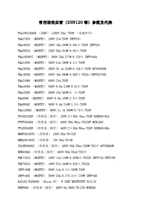
常用场效应管(25N120等)参数及代换FGA25N120AND (IGBT) 1200V/25A//TO3P (电磁炉用)FQA27N25 (MOSFET) 250V/27A/TO3P IRFP254FQA40N25 (MOSFET) 250V/40A/280W/0.051Ω/TO3P IRFP264FQA55N25 (MOSFET) 250V/55A/310W/0.03Ω/TO3PFQA18N50V2 (MOSFET) 500V/20A/277W/0.225Ω IRFP460AFQA24N50 (MOSFET) 500V/24A/290W/0.2Ω/TO3PFQA28N50 (MOSFET) 500V/28.4A/310W/0.126Ω/TO3P MTY30N50EFQL40N50 (MOSFET) 500V/40A/560W/0.085Ω/TO264 IRFPS37N50FQA24N60 (MOSFET) 600V/24A/TO3PFQA10N80 (MOSFET) 800V/9.8A/240W/0.81Ω/TO3PFQA13N80 (MOSFET) 800V/13A/300W/0. Ω/TO3PFQA5N90 (MOSFET) 900V/5.8A/185W/2.3Ω/TO3PFQA9N90C (MOSFET) 900V/8.6A/240W/1.3Ω/TO3PFQA11N90C (MOSFET) 900V/11.4A/300W/0.75Ω/TO3PFFA30U20DN (快恢复二极管) 200V/2×30A/40ns/TO3P DSEK60-02A FFPF30U60S (快恢复二极管) 600V/30A/90ns/TO220F MUR1560FFA30U60DN (快恢复二极管) 600V/2×30A/90ns/TO3P DSEK60-06A MBRP3010NTU (肖特基) 100V/30A/TO-220MBRA3045NTU (肖特基) 45V/30A/TO-3PISL9R3060G2 (快恢复二极管) 600V/30A/35ns/200W/TO247 APT30D60B RHRG3060 (快恢复二极管) 600V/30A/35nS/TO247FQP44N10 (MOSFET) 100V/44A/146W/0.0396Ω/TO220 IRF3710/IRF540N FQP70N10 (MOSFET) 100V/57A/160W/0.025Ω/TO220IRFP450B (MOSFET) 500V/14A/0.4Ω/205W/TO3PIRFP460C (MOSFET) 500V/20A/0.2~0.24Ω/235W IRFP460KA3162/FAN8800 (Drive IC)单IGBT/MOSFETFET驱动ICRHRP860 (快恢复二极管) 600V/8A/30NS/TO-220 MUR860RHRP1560 (快恢复二极管) 600V/15A/TO0220 MUR1560RHRP8120 (快恢复二极管) 1200V/8A/75W/TO220RHRP15120 (快恢复二极管) 1200V/15A/TO220RHRP30120 (快恢复二极管) 1200V/30A/125W/TO220单 DSEI20-10ARHRG30120 (快恢复二极管) 1200V/30A/T03PSSH45N20B (MOSFET) 200V/45A/TO3P IRFP260FGL40N150D (IGBT) 1500V/40A/TO264快速IGBTFGL60N100BNTD (IGBT) 1000V/60A/TO264快速IGBT 1MBH60-100HGTG10N120BND (IGBT) 1200V/35A/298W/100ns/TO247HGTG11N120CND (IGBT) 1200V/43A/298W/TO247HGTG18N120BND (IGBT) 1200V/54A/390W/90ns/TO247FQP5N50C (MOSFET) 500V/5A/73W/1.4Ω/TO-220 替代:IRF830,用于35W FQPF5N50C (MOSFET) 500V/5A/38W/1.4Ω/TO-220F 替代:IRF830,用于35W FQP9N50C (MOSFET) 500V/9A/135W/0.6Ω/TO220 替代:IRF840,用于75W FQPF9N50C (MOSFET) 500V/9A/44W/0.6Ω/TO-220F 替代:IRF840,用于75W FQP13N50 (MOSFET) 500V/13.4A/190W/0.43Ω/TO220 用于75W/125W产品FQPF13N50 (MOSFET) 500V/13.4A/48W/0.43Ω/TO220F 用于75W/125W产品FQD5N50C (MOSFET) 500V/5A/1.4Ω/TO252 用于35WFQA16N50 (MOSFET) 500V/16A/200W/0.32C/TO3P 用于150W到250W的产品FDP15N50 (MOSFET) 500V/15A/0.43Ω/56W/TO220 用于150W左右的产品FQP18N50V2 (MOSFET) 500V/18A/0.43Ω/208W/TO220 用于250WG到400W的产品FQPF18N50V2 (MOSFET) 500V/18A/0.43Ω/56W/TO220 用于250WG到400W的产品FQA18N50V2 (MOSFET) 500V/20A/277W/0.225Ω/TO3P 用于250WG到400W的产品FQA24N50 (MOSFET) 500V/24A/290W/0.2Ω/TO3P 用于400W的产品FQA24N60 (MOSFET) 600V/23.5A/310W/0.24Ω/TO3P 用于400W的产品FQA28N50 (MOSFET) 500V/28.4A/310W/0.126Ω/TO3P 用于400W的产品FQL40N50 (MOSFET) 500V/40A/560W/0.085Ω/TO264 用于560W的产品IRF740B (MOSFET) 400V/10A/0.55Ω/134W/TO220IRF730B (MOSFET) 400V/5.5A/1.0Ω/73W/TO220IRF830B (MOSFET) 500V/4.5A/1.5Ω/73W/TO220 IRF840B (MOSFET) 500V/8A/0.85Ω/134W/TO220 IRFP450B (MOSFET) 500V/14A/0.4Ω/205W/TO3P IRFP460C (MOSFET) 500V/20A/0.2~0.24Ω/235W FQPF5N60C (MOSFET) 600V/5A/TO220FFQPF8N60C (MOSFET) 600V/8A/TO220FFQPF10N60C (MOSFET) 600V/10A/TO220FQPF12N60 (MOSFET) 600V/12A/51W/0.65Ω/TO220F FCP11N60 (MOSFET) 650V/11A/125W0.32Ω/TO220 RHRD660S (快恢复二极管) 600V/6A/TO-252RHRP860 (快恢复二极管) 600V/8A/75W/TO-220 RHRP1560 (快恢复二极管) 600V/15A/TO-220单2N7002 (三极管) 60V/0.12A/SOT-23HUF76629D3S (MOSFET) 100V/20A/110W/TO-252 HUF75639S3S (MOSFET) 100V/56A/200W/TO-263ISL9V3040D3S (IGBT) 430V/21A/150W/300MJ/TO252 ISL9V3040S3S (IGBT) 430V/21A/150W/300MJ/TO263 ISL9V5036S3S (IGBT) 360V/46A/250W/TO262FQP33N10L (MOSFET) 100V/33A/52MΩ127W/TO220。
Vaisala GMW90 二氧化碳和温度传感器说明书

GMW90 CO2 and Temperature Transmitter - BACnet/Modbus1234567891011Vaisala Carbocap ® CO2 and Temperature Transmitter GMW905000Price5Display and colour Standard White (RAL9003, solid cover)0Standard White (RAL9003, display cover)1Black (RAL9005, solid cover)2Black (RAL9005, display cover)3No logo, standard White (RAL9003, solid cover)8No logo, standard White (RAL9003, display cover)9Indicator cover (RAL9003, display and CO2 indicators)A6Units MetricA Non metricB 7Display configuration Default (T, CO2)A CO2CO2C8Elevation setting Standard (sea level)0Custom Define m (ft)X 9CO2 indicator levels None0Standard (800,1200 ppm)1Custom Define YellowRed ppmX 10Trimmers With adjustement trimmerA No adjustement trimmerB11Quick reference guide No manual0Multilingual for digital devices 2Accessories:TM10SP Temperature measurement module GM10SP CO2 measuremnt module219980Connection cable for HM70 hand-held meter 219690USB cable for PC connectionSelections in bold are included in the prices of the basic versions Selections in italic are available at an extra costGMW9050001A A 00A 2GMW90 CO2 and Temperature Transmitter - Current output1234567891011Vaisala Carbocap ® CO2 and Temperature TransmitterGMW904Price2Output signal 4...20mA 3-wire 40...20mA 3-wire 53Output parameter for CH1CO20...2000 ppm L CO20...5000 ppm M CO2, free scaleDefine Low High ppm N T, free scaleDefine Low High °C (°F)T 4Output parameter for CH2T -5...+55 °C (+23...+131 °F)E T 0...+60 °C (+32...+140 °F)F CO2, free scaleDefine Low High ppm N T, free scaleDefine Low High °C (°F)T 5Display and colour Standard White (RAL9003, solid cover)0Standard White (RAL9003, display cover)1Black (RAL9005, solid cover)2Black (RAL9005, display cover)3No logo, standard White (RAL9003, solid cover)8No logo, standard White (RAL9003, display cover)9Indicator cover (RAL9003, display and CO2 indicators)A6Units Metric ANon metric B7Display configuration Default (T, CO2)ACO2C8Elevation setting Standard (sea level)0Custom Define m (ft)X9CO2 indicator levels None 0Standard(800,1200 ppm)1Custom Define Yellow Red ppmX 10Trimmers With adjustement trimmer ANo adjustement trimmer B11Quick reference guide No manual0Multilingual for analog devices 1Accessories:TM10SP Temperature measurement module GM10SP CO2 measuremnt module219980Connection cable for HM70 hand-held meter 219690USB cable for PC connectionSelections in bold are included in the prices of the basic versions Selections in italic are available at an extra costGMW9044L E 1A A 00A 1GMW90 CO2 and Temperature Transmitter - Voltage output1234567891011Vaisala Carbocap ® CO2 and Temperature TransmitterGMW903Price2Output signal 0...10 V 3-wire 20...5 V 3-wire 33Output parameter for CH1CO20...2000 ppm L CO20...5000 ppm M CO2, free scaleDefine Low High ppm N T, free scaleDefine Low High °C (°F)T 4Output parameter for CH2T -5...+55 °C (+23...+131 °F)E T 0...+60 °C (+32...+140 °F)F CO2, free scaleDefine Low High ppm N T, free scaleDefine Low High °C (°F)T 5Display and colour Standard White (RAL9003, solid cover)0Standard White (RAL9003, display cover)1Black (RAL9005, solid cover)2Black (RAL9005, display cover)3No logo, standard White (RAL9003, solid cover)8No logo, standard White (RAL9003, display cover)9Indicator cover (RAL9003, display and CO2 indicators)A6Units Metric ANon metric B7Display configuration Default (T, CO2)ACO2C8Elevation setting Standard (sea level)0Custom Define m (ft)X9CO2 indicator levels None 0Standard(800,1200 ppm)1Custom Define Yellow Red ppmX 10Trimmers With adjustement trimmer ANo adjustement trimmer B11Quick reference guide No manual0Multilingual for analog devices 1Accessories:TM10SPGM10SP Temperature measurement module219980Connection cable for HM70 hand-held meter 219690USB cable for PC connectionSelections in bold are included in the prices of the basic versions Selections in italic are available at an extra costGMW9032L E 1A A 00A 1。
Jamicon_SK系列规格书
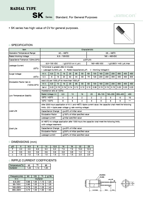
At +85oC no voltage application after 1000 hours the capacitor shall meet the following limits. (with voltage treatment) Shelf Life Capacitance Change Dissipation Factor Leakage current *±20% of initial value *200% of initial specified value *200% of initial specified value
*Whichever is greater after 3 minutes I : Leakage Current( µA) C : Rated Capacitance( µF) W.V. S.V. W.V. tan d 6.3 8 6.3 0.22 10 13 10 0.19 16 20 16 0.16 6.3 4 8 25 32 25 0.14 10 3 6 35 44 35 0.12 50 63 50 0.10 16 2 4 63 79 63
µF 0.47 1 2.2 3.3 4.7 10 22 33 47 100 220 330 470 1000 2200 3300 4700 6800 8200 10000 15000
Code
5x11 5x11 5x11 6.3x11 5x11 6.3x11 6.3x11 8x11.5 8x11.5 10x12.5 8x11.5 10x12.5 10x12.5 10x16 10x20 12.5x20 12.5x25 16x25 16x25 16x31.5 16x31.5 18x35.5 18x35.5 18x40 22x45 22x50 25x50
士林变频器SS2系列操作手册
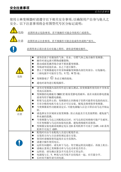
请勿对变频器内部的零件进行耐压测试,因变频器所使用的半导体易 受高压而损坏。
变频器的电路板有 CMOS IC 极易受静电的破坏,故在未做好静电措施 前请勿用手触摸电路板。
即使马达是停止的,变频器的主回路端子仍然可能带有危险的高压。 只有合格的电机专业人员才可以安装、配线及修理保养变频器。 当变频器某些功能被设定后,可能电源输入后会立即启动马达开始运
危险 注意
请勿存放于有腐蚀性气体、有水、引燃气体之场合操作变频器。 操作时请远离可燃物或爆裂物。 震动或摇晃激烈场合请不要放置变频器。 导线请勿浸泡在油、水之下进行操作。 禁止于变频器通电中用身体碰触变频器内部任何部分,以免触电。 三相电源不可接至 U/T1、V/T2、W/T3 端。
变频器端子 务必正确的接地。
2.1 铭牌说明 ................................................................................................................................................. 2 2.2 型号说明 ................................................................................................................................................. 2 2.3 订货代号说明...................................................................................................................
APT4F120S 1200V 4A 4.2Ω 高速高压N型切换电容电阻MOSFET(FREDFET
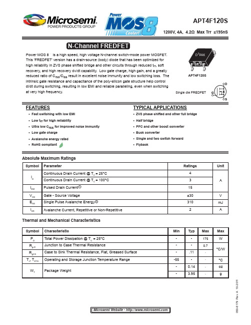
050-8179 R e v A 10-2011Absolute Maximum RatingsThermal and Mechanical CharacteristicsSymbol ParameterRatingsUnitI D Continuous Drain Current @ T C = 25°C 4A Continuous Drain Current @ T C = 100°C 3I DM Pulsed Drain Current 115V GS Gate - Source Voltage±30V E AS Single Pulse Avalanche Energy 2310mJ I ARAvalanche Current, Repetitive or Non-Repetitive2A Single die FREDFETTYPICAL APPLICATIONS•ZVS phase shifted and other full bridge •Half bridge•PFC and other boost converter •Buck converter•Single and two switch forward •FlybackFEATURES•Fast switching with low EMI •Low t rr for high reliability•Ultra low C rss for improved noise immunity •Low gate charge •Avalanche energy rated •RoHS compliantAPT4F120SPower MOS 8™ is a high speed, high voltage N-channel switch-mode power MOSFET.This 'FREDFET' version has a drain-source (body) diode that has been optimized for high reliability in ZVS phase shifted bridge and other circuits through reduced t rr , soft recovery, and high recovery dv/dt capability. Low gate charge, high gain, and a greatly reduced ratio of C rss /C iss result in excellent noise immunity and low switching loss. The intrinsic gate resistance and capacitance of the poly-silicon gate structure help control di/dt during switching, resulting in low EMI and reliable paralleling, even when switching at very high frequency.N-Channel FREDFETMicrosemi Website - Symbol CharacteristicMin Typ MaxMax P D Total Power Dissipation @ T C = 25°C --175W R θJC Junction to Case Thermal Resistance--0.7°C/W R θCS Case to Sink Thermal Resistance, Flat, Greased Surface -.11T J , T STGOperating and Storage Junction Temperature Range -55-°C W TPackage Weight-0.14oz - 3.95g050-8179 R e v A 10-2011Static CharacteristicsT J = 25°C unless otherwise speci fi edSource-Drain Diode CharacteristicsDynamic CharacteristicsT J = 25°C unless otherwise speci fied 1 Repetitive Rating: Pulse width and case temperature limited by maximum junction temperature.2 Starting at T J = 25°C, L = 155.0mH, R G = 25Ω, I AS = 2A.3 Pulse test: Pulse Width < 380μs, duty cycle < 2%.4 C o(cr) is de fined as a fi xed capacitance with the same stored charge as C OSS with V DS = 67% of V (BR)DSS . 5 C o(er) is de fi ned as a fi xed capacitance with the same stored energy as C OSS with V DS = 67% of V (BR)DSS . To calculate C o(er) for any value of V DS less than V (BR)DSS, use this equation: C o(er) = -8.32E-8/V DS ^2 + 3.49E-8/V DS + 1.30E-10.6 R G is external gate resistance, not including internal gate resistance or gate driver impedance. (MIC4452)Microsemi reserves the right to change, without notice, the speci fi cations and information contained herein.APT4F120SSymbol ParameterTest Conditions Min TypMaxUnit V BR(DSS)Drain-Source Breakdown VoltageV GS = 0V, I D = 250μA1200V∆V BR(DSS)/∆T JBreakdown Voltage Temperature Coef fi cient Reference to 25°C, I D = 250μA1.41V/°C R DS(on)Drain-Source On Resistance 3V GS = 10V, I D = 2A 3.424.2ΩV GS(th)Gate-Source Threshold VoltageV GS = V DS , I D = 0.5mA 2.545V ∆V GS(th)/∆T JThreshold Voltage Temperature Coef fi cient -10mV/°CI DSS Zero Gate Voltage Drain Current V DS = 1200V V GS = 0VT J = 25°C 250μA T J = 125°C1000I GSSGate-Source Leakage CurrentV GS = ±30V±100nASymbolParameterTest Conditions MinTyp Max Unit g fs Forward Transconductance V DS = 50V, I D = 2A 4.5SC iss Input CapacitanceV GS = 0V, V DS = 25Vf = 1MHz1385pFC rss Reverse Transfer Capacitance 17 C oss Output Capacitance100C o(cr) 4Effective Output Capacitance, Charge Related V GS = 0V, V DS = 0V to 800V40C o(er) 5Effective Output Capacitance, Energy Related 20Q g Total Gate Charge V GS = 0 to 10V, I D = 2A,V DS = 600V43nCQ gs Gate-Source Charge 7Q gd Gate-Drain Charge 20t d(on)Turn-On Delay Time Resistive Switching V DD = 800V, I D = 2A R G = 10Ω 6 , V GG = 15V7.4nst r Current Rise Time 4.4t d(off)Turn-Off Delay Time 24t fCurrent Fall Time6.9Symbol ParameterTest ConditionsMin Typ Max UnitI S Continuous Source Current (Body Diode)4AI SM Pulsed Source Current (Body Diode) 115V SD Diode Forward Voltage I SD = 2A, T J = 25°C, V GS = 0V0.81.2V t rr Reverse Recovery TimeI SD = 2A 3 ,di SD /dt = 100A/μs,V DD = 100VT J = 25°C 170 195nST J = 125°C 330400Q rr Reverse Recovery ChargeT J = 25°C .510μCT J = 125°C 1.0I rrm Reverse Recovery Current T J = 25°C 6.0AT J = 125°C8.3dv/dtPeak Recovery dv/dtI SD ≤ 2A, di/dt ≤1000A μs, V DD = 800V,T J = 125°C20 V/nsMOSFET symbol showing the integral reverse p-n junction diode (body diode)050-8179 R e v A 10-20112468101214160.51.01.52.02.53.03.54.0246810APT4F120SV G S , G A T E -T O -S O U R C E V O L T A G E (V )g f s , T R A N S C O N D U C T A N C ER D S (O N ), D R A I N -T O -S O U R C E O N R E S I S T A N C EI D , D R A I N C U R R E N T (A )I S D , R E V E R S E D R A I N C U R R E N T (A )C , C A P A C I T A N C E (p F )I D , D R A I N C U R R E N T (A )I D , D R I A N C U R RV DS(ON), DRAIN-TO-SOURCE VOLTAGE (V)V DS , DRAIN-TO-SOURCE VOLTAGE (V)Figure 1, Output CharacteristicsFigure 2, Output CharacteristicsT J , JUNCTION TEMPERATURE (°C) V GS , GATE-TO-SOURCE VOLTAGE (V)Figure 3, R DS(ON) vs Junction Temperature Figure 4, Transfer CharacteristicsI D , DRAIN CURRENT (A) V DS , DRAIN-TO-SOURCE VOLTAGE (V)Figure 5, Gain vs Drain CurrentFigure 6, Capacitance vs Drain-to-Source Voltage Q g , TOTAL GATE CHARGE (nC)V SD , SOURCE-TO-DRAIN VOLTAGE (V)Figure 7, Gate Charge vs Gate-to-Source Voltage Figure 8, Reverse Drain Current vs Source-to-Drain Voltage3.02.52.01.51.00.5054321050-8179 R e v A 10-2011APT4F120SD 3PAK Package Outline1.22 (.048)1.32 (.052)4.98 (.196)5.08 (.200)1.47 (.058)1.57 (.062)2.67 (.105)2.84 (.112)0.46 (.018){3 Plcs}0.56 (.022)and Leads are Platedn 0.020 (.001)0.178 (.007)Dimensions in Millimeters (Inches)e3 100% Sn Plated00.100.200.300.400.500.600.700.8010-510-410-3 10-2 10 1.0-1 Z θJ C , T H E R M A L I M P E D A N C E (°C /W )RECTANGULAR PULSE DURATION (seconds)FIGURE 9. MAXIMUM EFFECTIVE TRANSIENT THERMAL IMPEDANCE, JUNCTION-TO-CASE vs. PULSE DURATION。
刀片材质
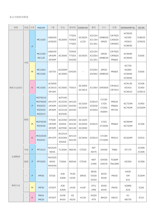
-
MCP3020
PVD
TiA N/
ALCrN
超多层
采用纳米级的TiA N和ALCrN的超多层覆膜“超级MCP涂层”与专
用的强韧性母材组合,是抗崩刃性和耐磨损性平衡结合的优异的
通用性材质,适用于普通钢、模具钢的普通加工。
◎
-
-
MCP3030
PVD
TiA N/
ALCrN
超多层
采用纳米级的TiA N和ALCrN的超多层覆膜“超级MCP涂层”与超
超多层
将强韧的母材与MZ涂层组合使用,适用于不锈钢加工。
-
◎
-
MZ2012
PVD
TiN+A N
超多层
将模具加工用的专用母材与MZ涂层组合使用,实现了优良耐磨性。
◎
◎
◎
MCP3010
CVD
Ti类微粒+
AL2O3
采用具有Ti类微粒覆膜的新型涂层,耐磨性和耐热龟裂性优异,
适用于普通~高速加工、湿式加工。
◎
K1
K8735
IC10
涂层说明
材质名
涂层
用途、特性
分类
P
M
K
MZ2031
PVD
TiN+A N
超多层
将耐磨损性的母材与MZ涂层组合使用,适合进行铸铁加工。
-
-
◎
MZ2033
PVD
TiN+A N
超多层
将强韧的母材与MZ涂层组合使用,可广泛应用于从普通钢到模具
钢的各种工件材料。
◎
-
-
MZ3035
PVD
TiN+A N
CR9025
KC9025
KC935
RL0805FR-070R51L;RL2512FK-07R018L;RL0805JR-070R22L;RL0402FR-070R68L;中文规格书,Datasheet资料
-
-
LPRC201 2322 ±1% 0.01 to 1 Ω 735 7xxxx
-
-
2010 LPRC111 2322 ±5% 0.01 to 0.0976 Ω 760 90xxx
-
-
LPRC111 2322 ±5% 0.1 to 1 Ω
760 60xxx
-
-
LPRC111 2322 ±1% 0.01 to 0.0976 Ω 761 90xxx
APPLICATIONS Converters Printer equipment Server board Telecom Consumer
FEATURES Halogen Free Epoxy RoHS compliant - Products with lead free terminations meet RoHS requirements - Pb-glass contained in electrodes, resistor element and glass are exempted by RoHS Reducing environmentally hazardous wastes High component and equipment reliability Saving of PCB space None forbidden-materials used in products/production Low resistances applied to current sensing
-
-
LPRC111 2322 ±1% 0.1 to 1 Ω
761 6xxxx
-
-
2512 LPRC221 2322 ±5% 0.01 to 0.0976 Ω 762 90xxx
多种电源管理芯片代换

1200AP40 1200AP60、1203P60200D6、203D6 DAP8A 可互代203D6/1203P6 DAP8A2S0680 2S08803S0680 3S08805S0765 DP104、DP7048S0765C DP704加24V的稳压二极管ACT4060 ZA3020LV/MP1410/MP9141ACT4065 ZA3020/MP1580ACT4070 ZA3030/MP1583/MP1591MP1593/MP1430 ACT6311 LT1937ACT6906 LTC3406/AT1366/MP2104AMC2576 LM2576AMC2596 LM2596AMC3100 LTC3406/AT1366/MP2104AMC34063A AMC34063AMC7660 AJC1564AP8012 VIPer12AAP8022 VIPer22ADAP02 可用SG5841 /SG6841代换DAP02ALSZ SG6841DAP02ALSZ SG6841DAP7A、DP8A 203D6、1203P6DH321、DL321 Q100、DM0265RDM0465R DM/CM0565RDM0465R/DM0565R 用cm0565r代换(取掉4脚的稳压二极管)DP104 5S0765DP704 5S0765DP706 5S0765DP804 DP904FAN7601 LAF0001LD7552 可用SG6841代(改4脚电阻)LD7575PS 203D6改1脚100K电阻为24KOB2268CP OB2269CPOB2268CP SG6841改4脚100K电阻为20-47KOCP1451 TL1451/BA9741/SP9741/AP200OCP2150 LTC3406/AT1366/MP2104OCP2160 LTC3407OCP2576 LM2576OCP3601 MB3800OCP5001 TL5001OMC2596 LM2596/AP1501PT1301 RJ9266PT4101 AJC1648/MP3202PT4102 LT1937/AJC1896/AP1522/RJ9271/MP1540SG5841SZ SG6841DZ/SG6841DSM9621 RJ9621/AJC1642SP1937 LT1937/AJC1896/AP1522/RJ9271/MP1540STR-G5643D STR-G5653D、STR-G8653DTEA1507 TEA1533TEA1530 TEA1532对应引脚功能接入THX202H TFC719THX203H TFC718STOP246Y TOP247YVA7910 MAX1674/75 L6920 AJC1610VIPer12A VIPer22A[audio01]ICE2A165(1A/650V.31W);ICE2A265(2A/650V.52W);ICE2B0565(0.5A/650V.23W):ICE2B165(1A/650V.31W);ICE2B265(2A/650V.52W);ICE2A180(1A/800V.29W);ICE2A280(2A/800.50W).KA5H0365R, KA5M0365R, KA5L0365R, KA5M0365RN# u) t! u1 W1 B) R, PKA5L0365RN, KA5H0380R, KA5M0380R, KA5L0380R1、KA5Q1265RF/RT(大小两种体积)、KA5Q0765、FSCQ1265RT、KACQ1265RF、FSCQ0765RT、FSCQ1565Q这是一类的,这些型号的引脚功能全都一样,只是输出功率不一样。
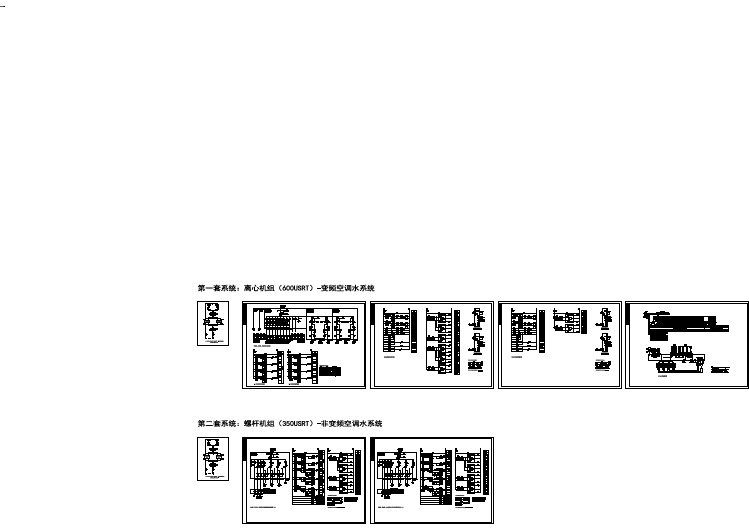
离心机组、螺杆机组中央空调水系统配电及控制原理图
赛米控丹佛斯电子 Board_93_GB_SKYPER_42_R 数据表

®Adaptor boardIGBT Driver CoreBoard 93 GB SKYPER 42 R Preliminary Data Features•Two output channels •Gold nickel finish •Failure managementTypical Applications*•Adaptor board for SKYPER 42 IGBT drivers in bridge circuits for industrial applications •PCB with gold plating •DC bus up to 1200VFootnotesIsolation test voltage with external high voltage diodeThe isolation test is not performed as a series test at SEMIKRONThe driver power can be expanded to 50µC with external boost capacitorsIsolation coordination in compliance with EN50178 PD2Operating temperature is real ambient temperature around the driver core Degree of protection: IP00This is an electrostatic discharge sensitive device (ESDS), international standard IEC 60747-1, Chapter IX* The specifications of our components may not be considered as an assurance of component characteristics. Components have to be tested for the respective application. Adjustments may be necessary. The use of SEMIKRON products in life support appliances and systems is subject to prior specification and written approval by SEMIKRON. We therefore strongly recommend prior consultation of our staff.Absolute Maximum Ratings SymbolConditionsValuesUnitV s Supply voltage primary 16V Iout PEAK Output peak current 30A Iout AVmax Output average current 150mA f max Max. switching frequency100kHz V CECollector emitter voltage sense across the IGBT1700V V isol IO Isolation test voltage input - output (AC, rms, 2s)4000V V isolPD Partial discharge extinction voltage, rms, Q PD ≤ 10pC1500V V isol12Isolation test voltage output 1 - output 2 (AC, rms, 2s)1500V R Gon min Minimum rating for external R Gon 0.8ΩR Goff min Minimum rating for external R Goff 0.8ΩT op Operating temperature -40...85°C T stgStorage temperature-40 (85)°CCharacteristics SymbolConditionsmin.typ.max.UnitV s Supply voltage primary side 14.41515.6V V i Input signal voltage on / off 15 / 0V V IT+Input treshold voltage HIGH 12.3V V IT-Input threshold voltage (LOW) 4.6V V G(on)Turn on output voltage 15V V G(off)Turn off output voltage-8V t d(on)IO Input-output turn-on propagation time 1.1µs t d(off)IOInput-output turn-on propagation time1.1µsAdaptor Board 93 SKYPER® 42 RTechnical ExplanationsRevision 04------------------------------------------------------------------------------------------------------------------------------------------------------------------------------------------ This Technical Explanation is valid for the following parts:Related documents:Prepared by: Johannes Krapp------------------------------------------------------------------------------------------------------------------------------------------------------------------------------------------ ContentApplication and Handling Instructions (2)Further application support (2)General Description (2)Dimensions (3)PIN Array (3)Setting Dynamic Short Circuit Protection (4)Collector Series Resistance (4)Adaptation Gate Resistors (5)Boost Capacitors (6)Environmental conditions (6)Mounting Notes (6)Please note:All values in this technical explanation are typical values. Typical values are the average values expected in large quantities and are provided for information purposes only. These values can and do vary in different applications. All operating parameters should be validated by user’s technical experts for each application.Application and Handling Instructions▪Please provide for static discharge protection during handling. As long as the hybrid driver is not completely assembled, the input terminals have to be short-circuited. Persons working with devices have to wear a grounded bracelet. Any synthetic floor coverings must not be statically chargeable. Even during transportation the input terminals have to be short-circuited using, for example, conductive rubber. Worktables have to be grounded. The same safety requirements apply to MOSFET- and IGBT-modules.▪Any parasitic inductances within the DC-link have to be minimised. Over-voltages may be absorbed by C- or RCD-snubber networks between main terminals for PLUS and MINUS of the power module.▪When first operating a newly developed circuit, SEMIKRON recommends to apply low collector voltage and load current in the beginning and to increase these values gradually, observing the turn-off behaviour of the free-wheeling diode and the turn-off voltage spikes generated across the IGBT. An oscillographic control will be necessary. Additionally, the case temperature of the module has to be monitored. When the circuit works correctly under rated operation conditions, short-circuit testing may be done, starting again with low collector voltage.▪It is important to feed any errors back to the control circuit and to switch off the device immediately in failure events.Repeated turn-on of the IGBT into a short circuit with a high frequency may destroy the device.▪The inputs of the hybrid driver are sensitive to over-voltage. Voltages higher than V S +0,3V or below -0,3V may destroy these inputs. Therefore, control signal over-voltages exceeding the above values have to be avoided.▪The connecting leads between hybrid driver and the power module should be as short as possible (max. 20cm), the driver leads should be twisted.Further application supportLatest information is available at . For design support please read the SEMIKRON Application Manual Power Modules available at .General DescriptionThe Board 93 GB SKYPER® 42 is an adaptor board for the IGBT module SKiM® 93 (spring contact). The board is paralleling three channels so the SKiM module can be used in half bridge configuration. The board can be customized allowing adaptation and optimization to the used IGBT module.The switching characteristic of the IGBT can be influenced through user settings, e.g. changing turn-on and turn-off speed by variation of R Gon and R Goff. Furthermore, it is possible to adjust the monitoring level and blanking time for the DSCP (see Technical Explanations SKYPER® 42 R).Please note:This technical explanation is based on the Technical Explanations for SKYPER®42 R. Please read the Technical Explanations SKYPER® 42 R before using the Adaptor Board.Dimensions116 PIN ArraySetting Dynamic Short Circuit ProtectionThe Vce formula for the Vce monitoring is described in the technical explanation of SKYPER 42 R. Collector Series ResistanceDesignation Shape SettingR105 MiniMELF (SMD) R VCE*Factory setting: not equippedTOPR205 MiniMELF (SMD) R VCE *Factory setting: not equippedBOTAdaptation Gate ResistorsBoost CapacitorsEnvironmental conditionsPlease refer to the technical explanation of SKYPER 42 R for the environmental conditions.Mounting NotesDISCLAIMERSEMIKRON reserves the right to make changes withoutfurnished in this document is believed to be accurate and reliable. However, no representation or warranty is given and no liability is assumed with respect to the accuracy or use of such information. SEMIKRON does not assume any liability arising out of the application or use of any product or circuit described herein. Furthermore,。
LM5022 60V 低侧控制器 20W BOOST 调节器示例模块说明书

User's GuideSNVA203C–January2007–Revised May2013AN-1557LM5022Evaluation Board The AN-1557is an evaluation module that demonstrates a typical20W Boost converter featuring the LM502260V low-side controller in a design that shows high efficiency in a single-ended application.Contents1Specifications Of The Board (2)2Example Circuit (2)3Powering The Converter (2)4Loading The Converter (2)5Enabling The Converter (2)6Testing The Converter (3)7MOSFET Footprints (3)8Permanent Components (4)9Additional Footprints (4)10Typical Performance Characteristics (6)11Bill of Materials (8)12PC Board Layout (9)List of Figures1Efficiency (2)2SO-8MOSFET Pinout (3)3Circuit Schematic (4)4Efficiency Measurement Setup (4)5Output Voltage Ripple Measurement Setup (5)6Switch Node Voltage(VIN =9V,IO=0.5A) (6)7Switch Node Voltage(VIN =16V,IO=0.5A) (6)8Output Voltage Ripple AC Coupled(VIN =9V,IO=0.5A) (6)9Output Voltage Ripple AC Coupled(VIN =16V,IO=0.5A) (6)10Load Transient Response(VIN =9V,IO=50mA to0.5A) (6)11Load Transient Response(VIN =16V,IO=50mA to0.5A) (6)12Start Up(VIN =9V,IO=0.5A) (7)13Shut Down(VIN =9V,IO=0.5A) (7)14Start Up(VIN =16V,IO=0.5A) (7)15Shutdown(VIN =16V,IO=0.5A) (7)16NGATE Rise Time(VIN =9V,IO=0.1A,Si4850DY) (7)17NGATE Fall Time(VIN =12V,IO=0.1A,Si4850DY) (7)18Top Layer and Top Overlay (9)19Bottom Layer (9)All trademarks are the property of their respective owners.1 SNVA203C–January2007–Revised May2013AN-1557LM5022Evaluation Board Submit Documentation FeedbackCopyright©2007–2013,Texas Instruments IncorporatedSpecifications Of The Board 1Specifications Of The BoardThe Evaluation Board has been designed for testing of various circuits using the LM5022boost regulator controller.A complete schematic for all the components is shown in Figure3.The board is two layers with components and power paths in1oz.copper.The board is62mil FR4laminate,and a complete bill ofmaterials is listed at the end of this document.2Example CircuitThe example circuit which comes on the evaluation board delivers a40V±2%output voltage at currents up to500mA and switches at500kHz.The input voltage range is optimized between9.0V and16.0V.The measured efficiency of the converter is95%at an input voltage of16V and an output current of0.5A.Figure1.Efficiency3Powering The ConverterThe example circuit for the LM5022Evaluation Board is optimized to run at12V,however the circuit will operate with input voltages ranging from6.0V to32.0V connected between the VIN and GND terminals on the right side of the board.4Loading The ConverterThe example circuit will startup with no load at the output,and can also start up with loads of up to0.5A as long as the input voltage is above9.0V.The maximum output current will be reduced for input voltages below9.0V.Fixed loads,resistors,and variable electronic loads can be connected between the Vo and GND terminals on the left side of the board.5Enabling The ConverterThe OFF terminal controls the state of the converter while power is applied to the input terminals.TheLM5022is disabled whenever the voltage at OFF is a logic high.(Above2.0V.)The LM5022is enabled whenever the OFF terminal is open-circuited or connected to ground,in which case startup will begin as soon as the input voltages exceeds6.0V.Upon enabling the LM5022will perform a soft-start,after which the output is ready to supply current to the load.2AN-1557LM5022Evaluation Board SNVA203C–January2007–Revised May2013Submit Documentation FeedbackCopyright©2007–2013,Texas Instruments IncorporatedS S S G D D D D Testing The Converter 6Testing The ConverterFigure4shows a block diagram of connections for making measurements of efficiency.The wires used for making connections at both the input and output should be rated to at least10A of continuous current and should be no longer than is needed for convenient testing.A series ammeter capable of measuring10A or more should be used for both the input and the output lines.Dedicated voltmeters should be connected with their positive and negative leads right at the four power terminals at the sides of the evaluation board.This measurement technique minimizes the resistive loss in the wires that connect the evaluation board to the input power supply and the electronic load.Output voltage ripple measurements should be taken directly across the100nF ceramic capacitor Cox, placed right between the output terminals.Care must be taken to minimize the loop area between theoscilloscope probe tip and the ground lead.One method to minimize this loop is to remove the probe’s spring tip and‘pigtail’ground lead and then wind bare wire around the probe shaft.The bare wire should contact the ground of the probe,and the end of the wire can then contact the ground side of Cox.Figure5 shows a diagram of this method.7MOSFET FootprintsThe LM5022evaluation board has a footprint for a single MOSFET with an SO-8package using theindustry standard pinout.(See Figure2)This footprint can also accept newer MOSFET packages that are compatible with SO-8footprints.Figure2.SO-8MOSFET Pinout3 SNVA203C–January2007–Revised May2013AN-1557LM5022Evaluation Board Submit Documentation FeedbackCopyright©2007–2013,Texas Instruments IncorporatedVoltmeterVoltmeterPermanent Components 8Permanent ComponentsThe following components should remain the same for any new circuits evaluated on the LM5022evaluation board:Name Value Cox,Cinx0.1µF Cf 1µF Csns 1nF Rpd 10k ΩRs1100Ω9Additional FootprintsThe 100pF capacitor Csyc provides an AC input path for external clock synchronization.Detection of the sync pulse requires a peak voltage level greater than 3.8V at the RT/SYNC pin.Note that the DC voltage at RT/SYNC is approximately 2V to allow compatibility with 3.3V logic.The sync pulse width should be set between 15ns to 150ns by the external components.The Rt resistor is always required,whether theoscillator is free running or externally synchronized.Rt must be selected so that the free-running oscillator frequency is below the lowest synchronization frequency.Figure 3.Circuit SchematicFigure 4.Efficiency Measurement Setup4AN-1557LM5022Evaluation BoardSNVA203C–January 2007–Revised May 2013Submit Documentation FeedbackCopyright ©2007–2013,Texas Instruments IncorporatedCox Additional FootprintsFigure 5.Output Voltage Ripple Measurement Setup5SNVA203C–January 2007–Revised May 2013AN-1557LM5022Evaluation Board Submit Documentation FeedbackCopyright ©2007–2013,Texas Instruments Incorporated1 és/DIV V O50 mV/DIV 1 és/DIV50 mV/DIV1 és/DIVSW10V/DIV 10V/DIV1 és/DIVSW10V/DIV10V/DIVTypical Performance Characteristics 10Typical Performance CharacteristicsFigure 6.Switch Node VoltageFigure 7.Switch Node Voltage(V IN =9V,I O =0.5A)(V IN =16V,I O =0.5A)Figure 8.Output Voltage Ripple AC CoupledFigure 9.Output Voltage Ripple AC Coupled(V IN =9V,I O =0.5A)(V IN =16V,I O =0.5A)6AN-1557LM5022Evaluation BoardSNVA203C–January 2007–Revised May 2013Submit Documentation FeedbackCopyright ©2007–2013,Texas Instruments Incorporated400 és/DIVI 5V/DIV20V/DIV20V/DIV2A/DIV200 és/DIVV I 5V/DIVSW OFF*20V/DIV20V/DIV2A/DIV400 és/DIV1V/DIV5V/DIVSWOFF*20V/DIV20V/DIV2A/DIV 200 és/DIV5V/DIVSWOFF*20V/DIV20V/DIV2A/DIV400 és/DIV V 2V/DIV200 mA/DIV1 ms/DIVV 1V/DIVI 200 mA/DIV Typical Performance CharacteristicsFigure 10.Load Transient ResponseFigure 11.Load Transient Response(V IN =9V,I O =50mA to 0.5A)(V IN =16V,I O =50mA to 0.5A)Figure 12.Start Up Figure 13.Shut Down (V IN =9V,I O =0.5A)(V IN =9V,I O =0.5A)Figure 14.Start Up Figure 15.Shutdown (V IN =16V,I O =0.5A)(V IN =16V,I O =0.5A)7SNVA203C–January 2007–Revised May 2013AN-1557LM5022Evaluation BoardSubmit Documentation FeedbackCopyright ©2007–2013,Texas Instruments Incorporated20 ns/DIVNGATE2V/DIV20 ns/DIV2V/DIVBill of Materials Figure 16.NGATE Rise Time Figure 17.NGATE Fall Time (V IN =9V,I O =0.1A,Si4850DY)(V IN =12V,I O =0.1A,Si4850DY)11Bill of MaterialsID Part Number TypeSize ParametersQty Vendor U1LM5022Low-Side ControllerVSSOP-101TI Q1Si4850EY MOSFET SO-860V,31m Ω,27nC1Vishay D1CMSH2-60M Schottky DiodeSMA 60V,2A 1Central SemiL1SLF12575T-330M3R2Inductor 12.5x12.533µH,3.2A,40m Ω1Pulse x7.5mm Cin1C4532X7R1H475M Capacitor 1812 4.7µF,50V 2TDK Cin2Co1Co2C5750X7R2A475M Capacitor 2220 4.7µF,100V,2m Ω2TDK Cf C3216X7R1E105K Capacitor 12061µF,25V 1TDK Cinx C2012X7R2A104M Capacitor 0805100nF,100V 2TDK Cox Cc1VJ0805Y561KXXAT Capacitor 0805560pF 10%1Vishay Cc2VJ0805Y124KXXAT Capacitor 0805120nF 10%1Vishay Css VJ0805Y103KXXAT Capacitor 080510nF 10%1Vishay Csns VJ0805Y102KXXAT Capacitor 08051nF 10%1Vishay Csyc VJ0805A101KXXAT Capacitor 0805100pF 10%1Vishay Rc CRCW08053011F Resistor 0805 3.01k Ω1%1Vishay Rfb1CRCW08056490F Resistor 0805649Ω1%1Vishay Rfb2CRCW08052002F Resistor 080520k Ω1%1Vishay Rs1CRCW0805101J Resistor 0805100Ω5%1Vishay Rs2CRCW08053571F Resistor 0805 3.57k Ω1%1Vishay Rsns ERJL14KF10C Resistor 12100.1Ω1%,0.5W 1Vishay Rt CRCW08053322F Resistor 080533.2k Ω1%1Vishay Ruv1CRCW08052611F Resistor 0805 2.61k Ω1%1Vishay Ruv1CRCW08051002FResistor 080510k Ω1%1Vishay Ruv2VIN,Vo 160-1026Terminal0.094”4CambionGND GND2GND3160-1512Terminal 0.062”4CambionGND4OFF SYNC8AN-1557LM5022Evaluation BoardSNVA203C–January 2007–Revised May 2013Submit Documentation FeedbackCopyright ©2007–2013,Texas Instruments Incorporated PC Board Layout 12PC Board LayoutFigure18.Top Layer and Top OverlayFigure19.Bottom Layer9 SNVA203C–January2007–Revised May2013AN-1557LM5022Evaluation Board Submit Documentation FeedbackCopyright©2007–2013,Texas Instruments IncorporatedIMPORTANT NOTICETexas Instruments Incorporated and its subsidiaries(TI)reserve the right to make corrections,enhancements,improvements and other changes to its semiconductor products and services per JESD46,latest issue,and to discontinue any product or service per JESD48,latest issue.Buyers should obtain the latest relevant information before placing orders and should verify that such information is current and complete.All semiconductor products(also referred to herein as“components”)are sold subject to TI’s terms and conditions of sale supplied at the time of order acknowledgment.TI warrants performance of its components to the specifications applicable at the time of sale,in accordance with the warranty in TI’s terms and conditions of sale of semiconductor products.Testing and other quality control techniques are used to the extent TI deems necessary to support this warranty.Except where mandated by applicable law,testing of all parameters of each component is not necessarily performed.TI assumes no liability for applications assistance or the design of Buyers’products.Buyers are responsible for their products and applications using TI components.To minimize the risks associated with Buyers’products and applications,Buyers should provide adequate design and operating safeguards.TI does not warrant or represent that any license,either express or implied,is granted under any patent right,copyright,mask work right,or other intellectual property right relating to any combination,machine,or process in which TI components or services are rmation published by TI regarding third-party products or services does not constitute a license to use such products or services or a warranty or endorsement e of such information may require a license from a third party under the patents or other intellectual property of the third party,or a license from TI under the patents or other intellectual property of TI.Reproduction of significant portions of TI information in TI data books or data sheets is permissible only if reproduction is without alteration and is accompanied by all associated warranties,conditions,limitations,and notices.TI is not responsible or liable for such altered rmation of third parties may be subject to additional restrictions.Resale of TI components or services with statements different from or beyond the parameters stated by TI for that component or service voids all express and any implied warranties for the associated TI component or service and is an unfair and deceptive business practice. TI is not responsible or liable for any such statements.Buyer acknowledges and agrees that it is solely responsible for compliance with all legal,regulatory and safety-related requirements concerning its products,and any use of TI components in its applications,notwithstanding any applications-related information or support that may be provided by TI.Buyer represents and agrees that it has all the necessary expertise to create and implement safeguards which anticipate dangerous consequences of failures,monitor failures and their consequences,lessen the likelihood of failures that might cause harm and take appropriate remedial actions.Buyer will fully indemnify TI and its representatives against any damages arising out of the use of any TI components in safety-critical applications.In some cases,TI components may be promoted specifically to facilitate safety-related applications.With such components,TI’s goal is to help enable customers to design and create their own end-product solutions that meet applicable functional safety standards and requirements.Nonetheless,such components are subject to these terms.No TI components are authorized for use in FDA Class III(or similar life-critical medical equipment)unless authorized officers of the parties have executed a special agreement specifically governing such use.Only those TI components which TI has specifically designated as military grade or“enhanced plastic”are designed and intended for use in military/aerospace applications or environments.Buyer acknowledges and agrees that any military or aerospace use of TI components which have not been so designated is solely at the Buyer's risk,and that Buyer is solely responsible for compliance with all legal and regulatory requirements in connection with such use.TI has specifically designated certain components as meeting ISO/TS16949requirements,mainly for automotive use.In any case of use of non-designated products,TI will not be responsible for any failure to meet ISO/TS16949.Products ApplicationsAudio /audio Automotive and Transportation /automotiveAmplifiers Communications and Telecom /communicationsData Converters Computers and Peripherals /computersDLP®Products Consumer Electronics /consumer-appsDSP Energy and Lighting /energyClocks and Timers /clocks Industrial /industrialInterface Medical /medicalLogic Security /securityPower Mgmt Space,Avionics and Defense /space-avionics-defense Microcontrollers Video and Imaging /videoRFID OMAP Applications Processors /omap TI E2E Community Wireless Connectivity /wirelessconnectivityMailing Address:Texas Instruments,Post Office Box655303,Dallas,Texas75265Copyright©2013,Texas Instruments Incorporated。
Infineon IMW120R045M1 CoolSiC 1200V SiC Trench MOS
IMW120R045M1XKSA1IMW120R045M1IMW120R045M1CoolSiC™ 1200V SiC Trench MOSFET Silicon Carbide MOSFET Features∙ Very low switching losses∙ Threshold-free on state characteristic ∙ Wide gate-source voltage range∙ Benchmark gate threshold voltage, V GS(th) = 4.5V ∙ 0V turn-off gate voltage ∙ Fully controllable dV/dt∙ Commutation robust body diode, ready for synchronous rectification ∙ Temperature independent turn-off switching lossesBenefits∙ Efficiency improvement ∙ Enabling higher frequency ∙ Increased power density ∙ Cooling effort reduction∙ Reduction of system complexity and costPotential applications∙ Energy generationo Solar string inverter and solar optimizer∙ Industrial power supplieso Industrial UPS o Industrial SMPS∙ Infrastructure – Chargeo ChargerProduct validationQualified for industrial applications according to the relevant tests of JEDEC 47/20/22 Table 1 Key Performance and Package ParametersTypeV DS I D(T C = 25°C, R th(j-c,max))R DS(on) (T vj = 25°C, I D = 20A, V GS = 15V)T j,max Marking Package IMW120R045M11200V52A 45mΩ175°C12M1045PG-TO247-3Drain pin 2Source pin 3Gate pin 1IMW120R045M1CoolSiC™ 1200V SiC Trench MOSFETTable of contentsTable of contentsFeatures (1)Benefits (1)Potential applications (1)Product validation (1)Table of contents (2)1Maximum ratings (3)2Thermal resistances (4)3Electrical Characteristics (5)3.1Static characteristics (5)3.2Dynamic characteristics (6)3.3Switching characteristics (7)4Electrical characteristic diagrams (8)5Package drawing (14)6Test conditions (15)Revision history (16)IMW120R045M1CoolSiC™ 1200V SiC Trench MOSFETMaximum ratings1Maximum ratingsFor optimum lifetime and reliability, Infineon recommends operating conditions that do not exceed 80% of the maximum ratings stated in this datasheet.1 verified by design2 Important note: The selection of positive and negative gate-source voltages impacts the long-term behavior of the device. The design guidelines described in Application Note AN2018-09must be considered to ensure sound operation of the device over the planned lifetime.IMW120R045M1CoolSiC™ 1200V SiC Trench MOSFET Thermal resistances2Thermal resistancesIMW120R045M1CoolSiC™ 1200V SiC Trench MOSFET Electrical Characteristics3Electrical Characteristics 3.1Static characteristicsvjIMW120R045M1CoolSiC™ 1200V SiC Trench MOSFETElectrical Characteristics3.2Dynamic characteristicsTable 5Dynamic characteristics (at T vj = 25°C, unless otherwise specified)GS,onIMW120R045M1CoolSiC™ 1200V SiC Trench MOSFETElectrical Characteristics3.3Switching characteristicsTable 6Switching characteristics, Inductive load 44 The chip technology was characterized up to 200 kV/µs. The measured dV/dt was limited by measurement test setup and package.IMW120R045M1CoolSiC™ 1200V SiC Trench MOSFETElectrical characteristic diagrams4 Electrical characteristic diagramsFigure 1Reverse bias safe operating area(RBSOA) (V gs = 0/15V, T c = 25°C, T j < 175°C)Figure 2 Power dissipation as a function of case temperature limited by bond wire (P tot = f(T C ))Figure 3Maximum DC drain to source current as a function of case temperature limited by bond wire (I DS = f(T C ))Figure 4 Maximum source to drain current as a function of case temperature limited by bond wire (I SD = f(T C ), V GS = 0V)IMW120R045M1CoolSiC™ 1200V SiC Trench MOSFET Electrical characteristic diagramsFigure 5Typical transfer characteristic(I DS = f(V GS), V DS = 20V, t P = 20µs) Figure 6Typical gate-source threshold voltage asa function of junction temperature(V GS(th) = f(T vj), I DS = 10mA, V GS = V DS)Figure 7Typical output characteristic, V GS asparameter (I DS = f(V DS), T vj=25°C, t P = 20µs) Figure 8Typical output characteristic, V GS asparameter (I DS = f(V DS), T vj=175°C, t P = 20µs)Figure 9Typical on-resistance as a function of junction temperature(R DS(on) = f(T vj), V GS=15V)Figure 10 Typical gate charge (V GS =f(Q G), I DS = 20A, V DS = 800V, turn-on pulse)Figure 11Typical capacitance as a function ofdrain-source voltage(C = f(V DS), V GS = 0V, f = 1MHz)Figure 12Typical body diode forward voltage as function of junction temperature(V SD=f(T vj), V GS=0V, I SD=20A)Figure 13Typical body diode forward current as function of forward voltage, V GS asparameter(I SD = f(V SD), T vj = 25°C, t P = 20µs)Figure 14Typical body diode forward current as function of forward voltage, V GS asparameter(I SD = f(V SD), T vj = 175°C, t P = 20µs)Figure 15Typical switching energy losses as afunction of junction temperature(E = f(T vj), V DD = 800V, V GS = 0V/15V,R G,ext = 2Ω, I D = 20A, ind. load, test circuit inFig. E, diode: body diode)Figure 16Typical switching energy losses as afunction of drain-source current(E = f(I DS), V DD = 800V, V GS = 0V/15V,R G,ext = 2Ω, T vj = 175°C, ind. load, test circuitin Fig. E, diode: body diode)Figure 17Typical switching energy losses as afunction of gate resistance(E = f(R G,ext), V DD = 800V, V GS = 0V/15V,I D = 20A, T vj = 175°C, ind. load, test circuit inFig. E, diode: body diode)Figure 18Typical switching times as a function of gate resistor(t = f(R G,ext), V DD = 800V, V GS = 0V/15V, I D = 20A,T vj = 175°C, ind. load, test circuit in Fig. E,diode: body diode)Figure 19Typical reverse recovery charge as afunction of diode current slope(Q rr = f(d i f/d t), V DD = 800V, I D = 20A, ind. load,test circuit in Fig.E)Figure 20Typical reverse recovery current as afunction of diode current slope(I rrm = f(d i f/d t), V DD = 800V, I D = 20A, ind. load,test circuit in Fig.E)Figure 21Max. transient thermal resistance (MOSFET/diode) (Z th(j-c,max) = f(t P), parameter D = t p/T, thermal equivalent circuit in Fig. D)Package drawing5Package drawingFigure 22Package drawingTest conditions6Test conditionsFigure 23Test conditions1200V SiC Trench MOSFET Revision historyRevision historyMajor changes since the last revisionTrademarksAll referenced product or service names and trademarks are the property of their respective owners.IMW120R045M1XKSA1。
APT15DQ120KG 1200V 15A 超快软恢复直流恢复矩阵体芯片数据手册说明书

Product OverviewThe APT15DQ120KG is a1200V,15A Ultrafast Soft Recovery Rectifier Si Diode in a TO-220package.FeaturesThe following are key features of the APT15DQ120KG device:•Ultrafast recovery times•Soft recovery characteristics•Low forward voltage•Low leakage current•Avalanche-energy rated•RoHS compliant•AEC-Q101qualifiedBenefitsThe following are benefits of the APT15DQ120KG device:•High switching frequency•Low switching losses•Low noise(EMI)switching•Higher reliability systems•Increased system power densityApplicationsThe APT15DQ120KG device is designed for the following applications:•Power factor correction(PFC)•Anti-parallel diode◦Switch-mode power supply◦Inverters/converters◦Motor controllers•Freewheeling diode◦Switch-mode power supply◦Inverters/converters•Snubber/clamp diodeThis section shows the specifications of the APT15DQ120KG device.Absolute Maximum RatingsThe following table shows the absolute maximum ratings of the APT15DQ120KG device.T C=25°C,unless otherwise specified.Table1•Absolute Maximum RatingsSymbolRatingParameterUnit V R1200V Maximum DC reverse voltageV RRMMaximum peak repetitive reverse voltageMaximum working peak reverse voltageV RWMI F(AV)15Maximum average forward current(T C=127°C,duty cycle=0.5)AI FSMNon-repetitive forward surge current(T J=45°C,8.3ms)110E AVLAvalanche-energy(1A,40mH)mJ20The following table shows the thermal and mechanical characteristics of the APT15DQ120KG device. Table2•Thermal and Mechanical CharacteristicsUnitMaxSymbolCharacteristicTypMinRθJCJunction-to-case thermal resistance1.18°C/WT J,T STGOperating and storage temperature range−55°C175T L300Lead temperature for10secondsWtPackage weight0.07oz1.9glbf•m Mounting torque,6-32or M3screw101.1N•mElectrical PerformanceThe following table shows the static characteristics of the APT15DQ120KG device.T J =25°C,unless otherwise specified.Table 3•Static CharacteristicsUnit Max Typ MinTest Conditions Characteristic Symbol V3.32.8I F =15A Forward voltageV F3.4I F =30A2.5I F =15A,T J =125°CµA100V R =1200VMaximum reverse leakage currentI RM500V R =1200V,T J =125°CpF 17V R =200VJunction capacitanceC JThe following table shows the dynamic characteristics of the APT15DQ120KG device.Table 4•Dynamic CharacteristicsUnit MaxTyp MinTest ConditionsCharacteristic Symbol ns21I F =1A;di F /dt =–100A/µs V R =30VReverse recovery timet rrns240I F =15A;di F /dt =–200A/µs V R =800VReverse recovery time t rr nC 260Reverse recovery chargeQ rr A 3Maximum reverse recovery current I RRM ns290I F =15A;di F /dt =–200A/µs V R =800V;T J =125°CReverse recovery time t rr nC 960Reverse recovery chargeQ rr A 6Maximum reverse recovery current I RRM ns130I F =15A;di F /dt =–1000A/µs V R =800V;T J =125°CReverse recovery time t rr nC 1340Reverse recovery chargeQ rr A19Maximum reverse recovery currentI RRMTypical Performance CurvesThis section shows the typical performance curves of the APT15DQ120KG device.Figure 1•Maximum Transient Thermal ImpedanceFigure 3•Reverse Recovery Time vs.Current Rate of ChangeFigure 2•Forward Current vs.Forward VoltageFigure 5 • Reverse Recovery Current vs. Current Rate of ChangeFigure 4 • Reverse Recovery Charge vs. Current Rate of ChangeFigure 7•Maximum Average Forward Current vs.Case TemperatureFigure 6 • Dynamic Parameters vs. Junction Temperature Figure 8•Junction Capacitance vs.Reverse VoltageThe following figure illustrates the diode test circuit of the APT15DQ120KG device.Figure9•Diode Test CircuitThe following figure illustrates the diode reverse recovery waveform and definitions of the APT15DQ120KGdevice.Figure10•Diode Reverse Recovery Waveform and Definitions1.I F—Forward conduction current.2.di F/dt—Rate of diode current change through zero crossing.3.I RRM—Maximum reverse recovery current.4.t rr—Reverse recovery time,measured from zero crossing where diode current goes from positive tonegative,to the point at which the straight line through I RRM and0.25•I RRM passes through zero.5.Q rr—Area under the curve defined by I RRM and t rr.This section shows the package specification of the APT15DQ120KG device. Package Outline DrawingThe following figure illustrates the TO-220package outline of the APT15DQ120KG device.Figure11•Package Outline DrawingThe following table shows the TO-220dimensions and should be used in conjunction with the package outline drawing.Table5•TO-220DimensionsMINSYMBOLMINMAXMAX[mm][mm][INCH][INCH]A4.320.1804.570.170B1.141.400.0550.0452.50C2.740.1080.098D0.360.0210.0140.53E2.650.1203.050.104F3.600.1563.960.14214.50G15.600.5710.614H2.390.1443.650.094I6.006.800.2680.2368.40J9.000.3540.33113.00K14.000.5510.512L1.231.390.0480.055M0.690.880.0350.027N10.0010.360.4080.394O7.570.3117.900.298P12.200.48013.100.516Q2.54BSC0.100BSCTERMINAL1CATHODEANODETERMINAL2CATHODETERMINAL3Microsemi's product warranty is set forth in Microsemi's Sales Order Terms and rmation contained in this publication is provided for the sole purpose of designing with and using Microsemi rmation regarding device applications and the like is provided only for your convenience and may be superseded by updates.Buyer shall not rely on any data and performance specifications or parameters provided by Microsemi.It is your responsibility to ensure that your application meets with your specifications.THIS INFORMATION IS PROVIDED "AS IS."MICROSEMI MAKES NO REPRESENTATIONS OR WARRANTIES OF ANY KIND WHETHER EXPRESS OR IMPLIED,WRITTEN OR ORAL,STATUTORY OR OTHERWISE,RELATED TO THE INFORMATION,INCLUDING BUT NOT LIMITED TO ITS CONDITION,QUALITY ,PERFORMANCE,NON-INFRINGEMENT,MERCHANTABILITY OR FITNESS FOR A PARTICULAR PURPOSE.IN NO EVENT WILL MICROSEMI BE LIABLE FOR ANY INDIRECT,SPECIAL,PUNITIVE,INCIDENTAL OR CONSEQUENTIAL LOSS,DAMAGE,COST OR EXPENSE WHATSOEVER RELATED TO THIS INFORMATION OR ITS USE,HOWEVER CAUSED,EVEN IF MICROSEMI HAS BEEN ADVISED OF THE POSSIBILITY OR THE DAMAGES ARE FORESEEABLE.TO THE FULLEST EXTENT ALLOWED BY LAW,MICROSEMI’S TOTAL LIABILITY ON ALL CLAIMS IN RELATED TO THIS INFORMATION OR ITS USE WILL NOT EXCEED THE AMOUNT OF FEES,IF ANY ,YOU PAID DIRECTLY TO MICROSEMI FOR THIS e of Microsemi devices in life support,mission-critical equipment or applications,and/or safety applications is entirely at the buyer’s risk,and the buyer agrees to defend and indemnify Microsemi from any and all damages,claims,suits,or expenses resulting from such use.No licenses are conveyed,implicitly or otherwise,under any Microsemi intellectual property rights unless otherwisestated.Microsemi2355W.Chandler Blvd.Chandler,AZ 85224USAWithin the USA:+1(480)792-7200Fax:+1(480)792-7277 ©2020Microsemi and its corporate affiliates.All rights reserved.Microsemi and the Microsemi logo are trademarks of Microsemi Corporation and its corporate affiliates.All other trademarks and service marks are the property of their respective owners.Microsemi Corporation,a subsidiary of Microchip Technology Inc.(Nasdaq:MCHP),and its corporate affiliates are leading providers of smart,connected and secure embedded control solutions.Their easy-to-use development tools and comprehensive product portfolio enable customers to create optimal designs which reduce risk while lowering total system cost and time to market.These solutions serve more than 120,000customers across the industrial,automotive,consumer,aerospace and defense,communications and computing markets.Headquartered in Chandler,Arizona,the company offers outstanding technical support along with dependable delivery and quality.Learn more at .053-4222|April 2020|ReleasedLegal。
APHBM2012SURKCGKC
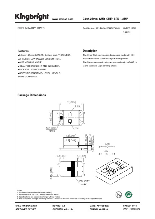
2.0x1.25mm SMD CHIP LED LAMP 洸子其科技是一家从事发光二极管产品研发、生产及销售公司,致力于为国内国际市场提供高品质,低成本的各类发光管。
主营产品有:SMD LED 0402、0603、0802、0805、1204、1206、3528、5050、3020、3014、2835、3535、335、020、正面发光及侧面发光,红、绿、蓝、白、黄、橙、粉红、紫、单色双色及三色等…主要应用:照明灯具、灯光亮化装饰工程、玩具礼品、背光显示、荧光验证防伪、手机、家电、MP3、手电筒、汽车、圣诞树、霓虹灯等…点击进入洸子其科技Selection GuidePart No.DiceLens TypeIv (mcd) [2] @ 20mA Viewing Angle [1] Min.Typ. 2θ1/2 APHBM2012SURKCGKC HYPER RED (InGaAlP) WATER CLEAR70 200 GREEN (InGaAIP)3680120°Electrical / Optical Characteristics at T A =25°CAbsolute Maximum Ratings at T A =25°CNote:1. 1/10 Duty Cycle, 0.1ms Pulse Width.Symbol Parameter DeviceTyp. Max. Units Test Conditionsλpeak Peak Wavelength Hyper Red Green 650 574 nm I F =20mA λD [1] Dominant Wavelength Hyper Red Green 635 570 nm I F =20mA Δλ1/2 Spectral Line Half-widthHyper Red Green 28 20 nm I F =20mA C Capacitance Hyper Red Green 35 15 pF V F =0V;f=1MHz V F [2] Forward Voltage Hyper Red Green 1.95 2.1 2.5 2.5 V I F =20mA I RReverse CurrentHyper Red Green10 10uAV R = 5VParameter Hyper RedGreen Units Power dissipation 75 75 mW DC Forward Current 30 30 mA Peak Forward Current [1] 185 150 mA Reverse Voltage55VOperating / Storage Temperature-40°C To +85°CNotes:1. Wavelength: +/-1nm.2. Forward Voltage: +/-0.1V.Notes:1. θ1/2 is the angle from optical centerline where the luminous intensity is 1/2 the optical centerline value.2. Luminous Intensity / Luminous Flux: +/-15%.。
STS232120U901电路保护器数据手册说明书
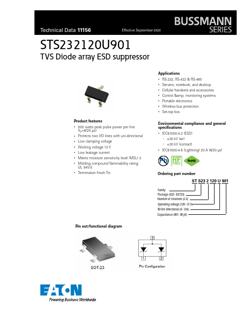
STS232120U901 TVS Diode array ESD suppressorProduct features• 500 watts peak pulse power per line(t P=8/20 µs)• Protects two I/O lines with uni-directional • Low clamping voltage• Working voltage:12 V• Low leakage current• Meets moisture sensitivity level (MSL) 3• Molding compound flammability rating: UL 94V-0• Termination finish:Tin Applications• RS-232, RS-422 & RS-485• Servers, notebook, and desktop• Cellular handsets and accessories• Control & monitoring systems• Portable electronics• Wireless bus protection• Set-top boxEnvironmental compliance and general specifications• IEC61000-4-2 (ESD)• ±30 kV (air)•±30 kV (contact)• IEC61000-4-5 (Lightning) 20 A (8/20 µs) Pb HALOGENHFFREEST S23 2 120 U 901FamilyPackage (S23- SOT23)Number of channels (2-2)Ordering part numberBi/Uni directional (U- Uni)Capacitance (901- 90 pF)Pin out/functional diagramOperating voltage (120- 12 V)2Technical Data 11156Effective September 2020STS232120U901 TVS Diode array ESD suppressor/electronicsSTS232120U901 ParameterSymbolValueUnitPeak pulse power dissipation on 8/20 μs waveform P pp 500W ESD per IEC 61000-4-2 (Air)ESD per IEC 61000-4-2 (Contact)V ESD +/-30+/-30kVLead soldering temperature T L +260 (10 seconds)°C Operating junction temperature range T J -55 to +125°C Storage temperature rangeT STG-55 to +150°CElectrical characteristics (+25 °C)STS232120U901 ParameterTest conditionMinimumTypicalMaximumSymbol (Units)Reverse working voltage ---12V RWM (V)Reverse breakdown voltage I T = 1 mA 13--V BR (V)Reverse leakage current V RWM = 12 V --0.15I R (μA)Clamping voltageI PP = 1 A, t p = 8/20 μs I PP = 20 A, t p = 8/20 μs --14231826V C (V)V C (V)Junction capacitanceV RWM = 0 V, f = 1 MHz Any I/O pin to GND V RWM = 0 V, f = 1 MHz Between I/O pins--9045--C J (pF)*C J (pF)*** C J measured at VRWM = 0 V, 1 MHz (pin1 to pin3, pin2 to pin3). **C J measured at VRWM = 0 V, 1 MHz (pin1 to pin2, pin2 to pin1).Absolute maximum ratings(+25 °C, RH=45%-75%, unless otherwise noted)Mechanical parameters, pad layout- mm/inchesPart markingMillimetersInches DimensionMinimumMaximumMinimumMaximumA 0.90 1.150.0350.045A10.000.100.0000.004b 0.250.3250.0100.013C 0.220.250.0090.010D 2.80 3.000.1100.118e 1.80 1.900.0710.075E 1.20 1.400.0470.055L 0.300.500.0120.020He 2.25 2.550.0890.100X 0.80 0.031X1 0.95 0.037Y 0.80 0.031Z2.020.0803Technical Data 11156Effective September 2020STS232120U901TVS Diode array ESD suppressor /electronics Packaging information mm/inchesDrawing not to scale.Supplied in tape and reel packaging, 3,000 parts per 7” diameter reel (EIA-481 compliant)4Technical Data 11156Effective September 2020STS232120U901 TVS Diode array ESD suppressor/electronicsRatings and V-I characteristic curves(+25 °C unless otherwise noted)V- I curve characteristics (Uni-directional)Pulse waveform (8/20 µs)Pulse derating curve ESD waveformEatonElectronics Division 1000 Eaton Boulevard Cleveland, OH 44122United States/electronics© 2020 EatonAll Rights Reserved Printed in USAPublication No. 11156 BU-MC20138September 2020Technical Data 11156Effective September 2020STS232120U901TVS Diode array ESD suppressor Life Support Policy: Eaton does not authorize the use of any of its products for use in life support devices or systems without the express writtenapproval of an officer of the Company. Life support systems are devices which support or sustain life, and whose failure to perform, when properly used in accordance with instructions for use provided in the labeling, can be reasonably expected to result in significant injury to the user.Eaton reserves the right, without notice, to change design or construction of any products and to discontinue or limit distribution of any products. Eaton also reserves the right to change or update, without notice, any technical information contained in this bulletin.Solder reflow profileT e m p e r a t u r eT LT PEaton is a registered trademark.All other trademarks are property of their respective owners.Follow us on social media to get the latest product and support information.Reference J-STD-020Profile featureStandard SnPb solderLead (Pb) free solderPreheat and soak • Temperature min. (T smin )100 °C 150 °C • Temperature max. (T smax )150 °C 200 °C • Time (T smin to T smax ) (t s )60-120 seconds 60-120 seconds Ramp up rate T L to T p 3 °C/ second max. 3 °C/ second max.Liquidous temperature (T l ) Time (t L ) maintained above T L183 °C60-150 seconds 217 °C60-150 seconds Peak package body temperature (T P )*Table 1Table 2Time (t p )* within 5 °C of the specified classification temperature (T c )20 seconds*30 seconds*Ramp-down rate (T p to T L ) 6 °C/ second max. 6 °C/ second max.Time 25 °C to peak temperature6 minutes max.8 minutes max.* Tolerance for peak profile temperature (T p ) is defined as a supplier minimum and a user maximum.Table 1 - Standard SnPb solder (T c )Package thicknessVolume mm3 <350Volume mm3 ≥350<2.5 mm 235 °C 220 °C ≥2.5 mm220 °C220 °CTable 2 - Lead (Pb) free solder (T c )Package thicknessVolume mm 3 <350Volume mm 3350 - 2000Volume mm 3 >2000<1.6 mm 260 °C 260 °C 260 °C 1.6 – 2.5 mm 260 °C 250 °C 245 °C >2.5 mm250 °C245 °C245 °C。
- 1、下载文档前请自行甄别文档内容的完整性,平台不提供额外的编辑、内容补充、找答案等附加服务。
- 2、"仅部分预览"的文档,不可在线预览部分如存在完整性等问题,可反馈申请退款(可完整预览的文档不适用该条件!)。
- 3、如文档侵犯您的权益,请联系客服反馈,我们会尽快为您处理(人工客服工作时间:9:00-18:30)。
SPECIFICATION FOR APPROV ALCUSTOMER: CUSTOMER’S P/N:VENDOR’S P/N: TL201209-2R7KA 2.0± 0.2 m/mB 1.2± 0.2 m/mC 0.9± 0.2 m/mD 0.5± 0.3 m/mE m/mF m/mG m/mH m/mI m/mJ m/mK m/mL m/mM m/mN m/mDIMENSION:(m/m)O m/mELECTRICAL REQUIREMENTSL 2.70 ± 10% μH TESTFREQ.10MHz/100mV Q 45 MIN. TESTFREQ.10MHz/100mVSrf 45 MHz MIN. TEST FREQ. MHzRdc 0.75 OHM. MAX. TEST FREQ. MHzIdc 30 mA MAX. TEST FREQ. MHzTEST INSTRUMENTS●HP 4338A MILLIOHMMETER○HP 4195A NETWORK/SPECTRUMANALYZER○HP 4284A BIAS CURRENT SOURCE○HP 4285A PRECISION LCR METER ○HP 4286A PRECISION LCR METER●HP 4291B RF IMPEDANCE/MATERIAL ANALYZER○HP 6632A DC POWER SUPPLY DRAWN BYJuli WangCHECKED BYJohn ChuangAPPROVED BYLionel LinTEST DATACUSTOMER:CUSTOMER’S P/N:SERIES NO: TL3059 VENDOR’S P/N:TL201209-2R7K DATE: MEAS A B C D L Q Rdc ITEM (m/m) (m/m) (m/m) (m/m) (μH) (Ω)SPEC 2.0 ± 0.21.2 ± 0.2 0.9 ±0.20.5±0.3 2.7 ±10%45 MIN. 0.75MAX. TESTFREQ. 10MHz10MHz1 2.00 1.23 0.93 0.50 2.56 65.6 0.4172 2.03 1.20 0.91 0.53 2.72 65.4 0.4213 2.04 1.22 0.89 0.52 2.64 62.4 0.4254 2.01 1.21 0.92 0.50 2.54 72.7 0.3965 2.00 1.23 0.90 0.51 2.58 68.5 0.4066 1.99 1.22 0.92 0.52 2.64 63.7 0.4157 2.02 1.20 0.89 0.53 2.60 71.2 0.4198 2.03 1.23 0.91 0.48 2.67 66.8 0.4159 2.01 1.21 0.92 0.53 2.60 60.9 0.43610 2.00 1.22 0.90 0.52 2.59 63.3 0.428A VG. 2.01 1.22 0.91 0.52 2.61 66.1 0.418R 0.05 0.03 0.04 0.05 0.18 11.8 0.040DRAWN BYJuli Wang CHECKED BYJohn ChuangAPPROVED BYLionel LinTYPICAL ELECTRICAL CHARACTERISTICS CURVE TL2012 TypeInductance VS. Frequency Impedance VS. FrequencyInductance VS. Temperature Q VS. FrequencyRELIABILITY TESTItemPerformanceTest conditionOperating temperature range-55 o C to + 125 oC Storage temperature and umidity ranges 40 oC MAX., 70% RH MAX.Soldering heat resistanceThe chip shall not be cracks.More than 75% of terminal electrode shall be covered with solder.Preheat: 150 o C, 60 secondsSolder temperature : 260 ± 5 oC Flux: RosinDip time: 10 ± 1 secondsSolderabilityMore than 90% of the terminal electrode shall be covered with new solder.Preheat: 150 o C, 60 seconds Solder temperature: 245 ± 5 o C Flux: RosinDip time: 4 ± 1 seconds245℃Recommended Soldering Conditions(REFLOW TEMPERATURE PROFILE) Lead-FreeA 260 ± 5℃B 230 ± 5℃C 30 ± 10 secD 150℃ E180℃ F90 ± 30secRELIABILITY TESTTerminal strength The terminal electrode and the body shall not be damaged by the forces applied on the right conditions.Bending strengthType P (kgf) Time (s)T 100505 0.3T 160808 0.5T 201209 0.6T 201212 0.8T 321611 1.0T 322513 1.0 30± 5T 451616 1.0T 453215 1.5TA3216M4 0.5The body shall not be damaged by the forcesapplied on the right conditions.Type A (mm) P (kgf)P(N)T 160808 1.0 0.5T 201209 1.4 1.0T 201212 1.4 1.2T 321611 2.0 2.0T 322513 2.0 2.5T 451616 2.5 2.5T 453215 2.7 2.5TA3216M4 1.4 1.0RELIABILITY TESTItemPerformanceTest conditionHigh temperature resistanceAppearance : Ferrite shall not be damaged. Inductance : Within ±10% of the initial value. Q: Within ±30% of the initial value.Temperature: 85±2℃Testing time: 1008±12 hoursMeasurement: After placing for 24 hours minHumidity resistance Appearance: Ferrite shall not be damaged.Inductance: Within ±10% of the initial value Q: Within ±30 % of the initial value.Humidity: 90 to 95% RH Temperature: 40±2℃Testing time: 1008±12 hoursMeasurement: After placing for 24 hours minThermal ShockAppearance: Cracking, chipping or any other defects harmful to the characteristics shall not be allowed.Inductance: Within ±10% of the initial value Q: Within ±30% of the initial value.Temperature: -40℃, +85℃, kept stabilized for 30 minutes eachCycle: 100 cyclesMeasurement: After placing for 24 hours minLow temperaturestorage life testAppearance: Cracking, chipping or any other defects harmful to the characteristics shall not be allowed. Inductance: Within ±10% of the initial value. Q: Within ±30% of the initial value.Temperature: -40±2℃Testing time: 1008±12 hours Measurement: After placing for 24 hours minPACKAGINGz Tape dimensions and packaging quantitiesCarrier tape material: papermaterial: Paper ( Dimensions in mm)TYPE A B W P T CHIPS / REEL 100505 0.62 1.12 8 2 0.60 10000 160808 1.10 1.90 8 4 0.95 4000 201209 1.50 2.30 8 4 0.954000material: Polystyrene ( Dimensions in mm)TYPE A B W P T CHIPS /REEL 160808 1.01 1.80 8 4 1.02 4000 201209 1.42 2.25 8 4 1.04 4000 201212 1.50 2.35 8 4 1.45 2000 321611 1.88 3.50 8 4 1.273000z Reel dimensionsDimensions in mmTYPE 8mm 12mm A 178±2 178±2 B 21.0±0.8 21.0±0.8 C13.0±0.8 13.0±0.8G 10.0 14.0 N 75 75T 12.5 16.5。