operational amplifier basis
常用物料英文代码
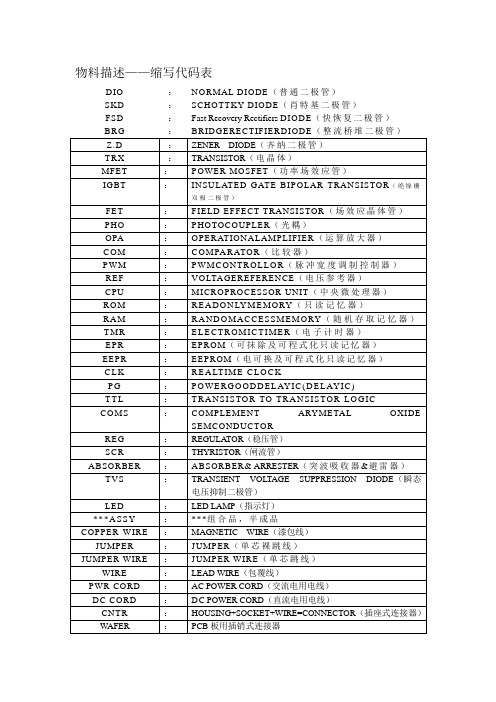
POLYFOAM PLATE LAYER(保丽龙板层)
PA BOX
:
PAPER BOX(纸盒)
GIFT BOX
:
GIFT BOX(礼盒)
SPONGE
:
SPONGE(海绵)
BUBBLE BAG
:
BUBBLE BAG(气泡袋)
ANTI-ELE BAG
:
ANTI-STATIC ELECTRICAL BAG(抗静电袋)
DC CORD
:
DC POWER CORD(直流电用电线)
CNTR
:
HOUSING+SOCKET+WIRE=CONNECTOR(插座式连接器)
WAFER
:
PCB板用插销式连接器
MINI JUMPER
:
小型短用插座
HOUSING
:
HOUSING
TERMINAL
:
TERMINAL(端子)
SCREW
:
SCREW(螺丝)
TRX
:
TRANSISTOR(电晶体)
MFET
:
POWER MOSFET(功率场效应管)
IGBT
:
INSULATED GATE BIPOLAR TRANSISTOR(绝缘栅双极二极管)
FET
:
FIELD EFFECT TRANSISTOR(场效应晶体管)
PHO
:
PHOTOCOUPLER(光耦)
OPA
VARNISH
:
凡立水
QUATZITE
:
石英砂
Comform Coating
:
三防漆
Hot Melt Adhesives
Operational Amplifiers

operational amplifier 运算放大器 input resistance 输入电阻 output resistance 输出电阻 high-gain 高增益 linear 线性的 feedback 反馈 network 网络 vacuum tube 电子管 external 外部的 compensate 补偿 nonideal 非理想的 behavior 行为 inverting input 反相输入端 non-inverting input 同相输入端 minus sign 减号 plus sign 加号 dc voltage 直流电压 supply voltage 电源电压 regulated dc power supplies 直流稳压电源 output load 输出负载
Two shorthand notations for op-amps are shown in Figure 5.16(b)and 5.16(c). In Figure5.16(b), the reference node is presumed; proper connections to supplies are presumed, and inputs and outputs are labeled with the appropriate node-toreference voltages. Often the supply, terminals are left off, as in Figure 5.16(c). However, this streamlined notation can be confusing, as explained below.
voltage gain 电压增益 voltage-controlled voltage source 电压控制电压源
美军雷达命名规则和雷达英文词汇e
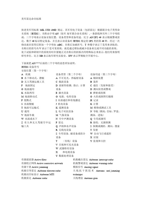
美军雷达命名标准按老美军用标准MIL-STD-196D规定,其军用电子设备〔包括雷达〕根据联合电子类型命名系统〔JETDS〕。
名称由字母AN〔陆军-海军联合命名系统〕,一条斜线和另外三个字母组成。
三个字母表示设备安装位置,设备类型和设备用途。
比方AN/SPS-49表示舰载警戒雷达。
数字49标识特定装备,并且表示该设备时JETDS规定的SPS类的第49种。
经过一次修改就在原型后附加一个字母如ABC,名称后加破折号,T和数字表示丫是用来训练的。
名称后的括号内V表示丫是可变系统,就是通过增加或减少设备来完成不同功能的系统。
处于试验和研制中的系统有时在紧随正式名称后的括弧内用特殊标志来表示,他们用来指明研究单位。
比方XB表示海军研究实验室,XW表示罗姆航空开展中心。
下面就把AN/***后面的三个字母的意思祥加说明。
JETDS设备符号安装位置〔第一个字母〕A 机载B 水下移动式,潜艇D 无人驾驶运载工具F 地面固定G 地面通用K 水陆两用M 地面移动式P 便携式S 水面舰艇T 地面可运输式U 通用V 地面车载W 水面或水下Z 有人和无人驾驶空中运输工具设备类型〔第二个字母〕A 不可见光,热辐射设备C 载波设备D 放射性检测,指示,计算设备E 激光设备G 电报,电传设备I 内部通信和有线播送J 机电设备K 遥测设备L 电子对抗设备M 气象设备N 空中声测设备P 雷达Q 声纳和水声设备R 无线电设备S 专用设备,磁设备或组合设备T 〔有线〕设备V 目视和可见光设备W 武器特有设备X 和电视设备Y 数据处理设备设备用途〔第三个字母〕A 辅助装置B 轰炸C 通信〔发射和接受〕D 测向侦查或警戒E 弹射或投掷G 火控或探照灯瞄准H 记录K 计算M 维修或测试工具N 导航〔测高,信标,罗盘,测深,进场〕Q 专用或兼用R 接收,无源探测S 探测或测距,测向,搜索T 发射W 自动飞行或遥控X 识别Y 监视和火控有源滤波器Active filter有源校正网络Active corrective network 有源干扰Active jamming机载引导雷达Airborne director radar 机载动目标显示Airborne MTI机载雷达Airborne radar 机载截击雷达Airborne-intercept radar机载警戒雷达Airborne warning radar模拟信号Analog signal天线抗干扰技术Antenna anti-jamming technique天线增益Antenna gain反辐射导弹Anti-radiation missile背射天线Backfire antenna回差Backlash 轰炸雷达Bombing radar 平衡电感Balancing inductor选频放大器Bandpass amplifier战场侦察雷达Battle-field search radar 盲区Blind zone闪烁干扰Blinking jamming击穿功率Breakdown power体效应二极管本地振荡器Bulk effect diode local oscillator宽带中频放大器Broad band intermediate frequency amplifier机柜、分机结构Cabinet, subassembly标定误差Calibrated error电子束管(阴极射线管) Cathode-ray tube(CRT)空腔型振荡器Cavity Oscillator谐振腔Cavity Resonator空腔稳频本地振荡器Cavity-Stabilized Local Oscillator干扰偶极子Chaff Dipole信道化接收机Channelized receiver圆极化平面波Circularly polarized plane wave闭环控制系统〔反应控制系统〕Close-loop control system (feed-back control system)杂波抑制Clutter suppression同轴电缆Coaxial cable 同轴谐振腔Coaxial cavity同轴定向耦合器Coaxial directional coupler 同轴滤波器Coaxial filter相干振荡器Coherent oscillator 相干动目标显示Coherent MTI复调制干扰Complex modulated jamming圆锥扫描雷达Conical scan radar圆锥扫描天线Conical Scanned Antenna连续波雷达接收机Continuous-wave radar receiver比照度Contrast 卷积器Convolutor变频损耗Conversion loss 相关时间Correlation time抗反辐射导弹措施Counter anti-radiation missile measures 正交场器件〔M型器件〕Crossed-field devices(M-type devices)截止式衰减器Cut-Off Attenutor截止波长Cut-off wavelength连续波雷达发射机CW Radar Transmitter直流阻抗D.C. impedance直流谐振充电D.C. resonant charging 直流谐振二极管充电D.C. resonant diode charge 数据处理Data processing偏转线圈Deflection coil延时充电电路Delayed charging circuit介质移相器Dielectric phase shifter介质干扰杆Dielectric chaff rod数字滤波器Digital filter数字匹配滤波器Digital matched filter数字测距Digital ranging引导雷达Director radar多普勒雷达Doppler Radar双门限检测器Double threshold detector 双T接头Double T-junction等效负载Dummy load 天线收发开关DuplexerE面〔H面〕折叠双T E plane (H plane) magic-T天线的有效面积Effective area of an antenna 有效辐射功率Effective radiation power(E.R.P.)电液伺服阀Electro-hydraulic Servo value电磁兼容性Electromagnetic compatibility 电子抗干扰Electronic anti-jamming电扫描天线Electronic Scanned antenna电扫描雷达Electronically Scanned Radar椭圆极化场矢量Elliptically Polarized Field Vector末制导雷达End-guidance radar鼓励器〔预调器、触发器〕Exciter(premodulator, trigger)极窄脉冲雷达Extra-short pulse radar快速付里叶变换Fast Fourier Transform馈电网络Feed network 相控阵馈电网络Feed networks For Phased Array铁氧体移相器Ferrite phase shifter火控雷达Fire control radar 频率捷变雷达Frequency agile radar调频雷达发射机Frequency modulation radar transmitter引信干扰Fuse jamming齿轮传动误差Gear transmission error图形失真校正Graphic distortion correction 格雷戈伦天线Gregarain antenna制导雷达Guidance radar炮瞄雷达Gun directing radar 盘旋管Gyrotron测高雷达Height-finding radar水平极化场矢量Horizontally polarized field vector喇叭天线Horn antenna 环行电桥Hybrid ring液压泵Hydraulic pump阻抗匹配Impedance match 天线阻抗匹配Impedance match of antenna输入阻抗Input impedance 天线罩插入相移Insertion phase of a radome阵列单元的孤立阻抗Isolated impedance of an array element天线间的隔离Isolation between antennas干扰压制系数Jamming blanket factor干扰调制样式Jamming modulation type干扰信号带宽Jamming signal band width速调管Klystron激光雷达Laser radar 线阵天线Linear array antenna 负载阻抗Load impedance低空搜索雷达Low altitude surveillance radar主振放大式发射机M.O.P.A. transmitter磁脉冲调制器Magnetic pulse modulator 磁控管Magnetron磁控管灯丝电压控制电路Magnetron filament voltage controlling Circuit主瓣零点宽度Main (major) lobe zero beamwidth航海雷达Marine radar 矩阵阵列Matrix array 气象雷达Meteorological radar微波带通滤波器Microwave band-pass filter 微波场效应晶体管放大器Microwave field effect transistor amplifier微波全息雷达Microwave hologram radar微波低通滤波器Microwave low-pass filter 副瓣电平Minor (side) lobe level机动雷达Movable radar 阵列天线的互耦Mutual coupling of an array antenna多模馈电器Multimode feed 多基地雷达Multistatic radar多端网络Multiport network导航雷达Navigation radar 噪声调幅干扰Noise AM jamming噪声调幅调相干扰Noise AM-PM jamming 归一化差斜率Normalized difference slope 单通道单脉冲雷达One-channel Monopulse Radar开环系统频率特性Open-loop system frequency characteristic运算放大器Operational Amplifier超视距雷达Over-the-horizon radar过压保护电路Overvoltage protection circuit 抛物柱面天线Parabolic cylindrical antenna 参量检测器Parameter detector无源雷达Passive radar相位检波器Phase detector 移相器Phase detector相控阵天线Phased array antenna 锁相接收机Phase-locked receiver相位扫描雷达Phase-scanned radar脉冲压缩雷达Pulse compression radar 脉冲雷达接收机Pulse radar receiver相控阵的量化误差Quantization error of a phased array雷达精度Radar accuracy 雷达反侦察Radar anti-reconnaissance天线罩Radome采样频率Sampling frequency 舰载雷达Shipbased radar船用雷达Shipboard radar 侧视雷达Side-looking radar旁瓣对消Sidelobe Cancellation固体微波振荡器Solid state microwave oscillator合成孔径雷达Synthetic radar目标识别雷达Target-identification radar三通道单脉冲雷达接收机Three-channel monopulse radar receiverT型〔Y型〕环行器〔结环行器〕T-type(Y-type) circulator (junction circulator)静电控制超高频电子管〔栅控管〕UHF electronstatic control tubeV形波束雷达V-beam radar压控晶体振荡器V oltage controlled oscillator 波导谐振腔Waveguide cavity天气雷达Weather radar X-Y型天线座X-Y type antenna pedestal八木天线Yagi antenna雷达覆盖范围Zone of radar coverage零轴漂移Zero-axsis drift雷达工作模式:目标捕获系统:The tention action system(该系统配备有嵌入式惯性导航系统和全球定位系统,可在雷达快速展开时提供雷达位置坐标。
电荷放大器
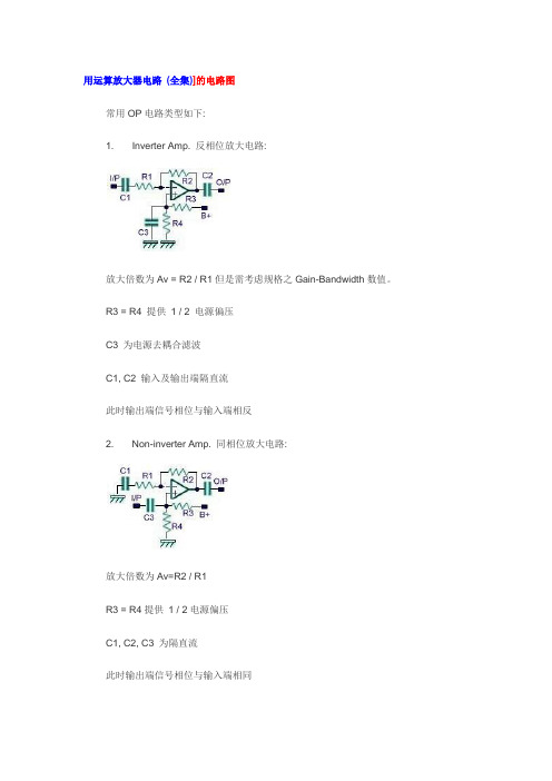
用运算放大器电路(全集)]的电路图常用OP电路类型如下:1. Inverter Amp. 反相位放大电路:放大倍数为Av = R2 / R1但是需考虑规格之Gain-Bandwidth数值。
R3 = R4 提供1 / 2 电源偏压C3 为电源去耦合滤波C1, C2 输入及输出端隔直流此时输出端信号相位与输入端相反2. Non-inverter Amp. 同相位放大电路:放大倍数为Av=R2 / R1R3 = R4提供1 / 2电源偏压C1, C2, C3 为隔直流此时输出端信号相位与输入端相同3. Voltage follower 缓冲放大电路:O/P输出端电位与I/P输入端电位相同单双电源皆可工作4. Comparator比较器电路:I/P 电压高于Ref时O/P输出端为Logic低电位I/P 电压低于Ref时O/P输出端为Logic高电位R2 = 100 * R1 用以消除Hysteresis状态, 即为强化O/P输出端, Logic高低电位差距,以提高比较器的灵敏度. (R1=10 K, R2=1 M)单双电源皆可工作5. Square-wave oscillator 方块波震荡电路:R2 = R3 = R4 = 100 KR1 = 100 K, C1 = 0.01 uFFreq = 1 /(2π* R1 * C1)6. Pulse generator脉波产生器电路:R2 = R3 = R4 = 100 KR1 = 30 K, C1 = 0.01 uF, R5 = 150 KO/P输出端On Cycle = 1 /(2π* R5 * C1)O/P输出端Off Cycle =1 /(2π* R1 * C1)7. Active low-pass filter 主动低通滤波器电路:R1 = R2 = 16 KR3 = R4 = 100 KC1 = C2 = 0.01 uF放大倍数Av = R4 / (R3+R4)Freq = 1 KHz8. Active band-pass filter 主动带通滤波器电路:R7 = R8 = 100 K, C3 = 10 uFR1 = R2 = 390 K, C1 = C2 = 0.01 uFR3 = 620, R4 = 620KFreq = 1 KHz, Q=259. Window detector窗型检知器电路:当I/P电位高于OP1+端电位时, Led 1暗/Led 2亮当I/P电位高于OP2-端电位时, Led 1亮/Led 2暗只有当I/P电位高于OP2-端电位, 却又低于OP1+端电位时, Led 1与Led 2同时皆亮如果适当选择R1, R2,R3数值可用以检知I/P电位是否合乎规格。
电化学工作站原理及应用

内容
恒电位仪的原理
1、溶液等效电路与三电极体系 2、电子线路基础 3、恒电位仪典型电路与结构 4、恒电位仪主要技术参数
法国雷氏恒电位仪voltalab50
恒电位仪
EG&G PARC
263
2263
273
2273
Autolab
BAS 100W
恒电位仪 WE RE CE
WE:工作电极/研究电极 RE: 参比电极 CE: 辅助电极/对电极
④ 汞滴表面积可准确测量,S 0 .0 0 8 5 2 m 2 3 t2 3/cm2,
m为滴汞流速(mg/s),t为时间(s)
滴Hg电极的缺点
➢ 被测体系的浓度有一定的限制
浓度不能太小,若<10-5 M,汞滴面积变化引起的电容电 流影响较大; 浓度也不能太大,若>0.1 M,汞滴不宜滴落; 合适的浓度范围是:0.01<[C]<0.1 M
Hg|Hg2SO4|SO42-
H g 2 S O 4 2 e 2 H g S O 4 2
0
RT 2F
ln aSO42
亚汞不稳定,高温时易变成Hg2+,受温度影响大。防止Hg2SO4水解,应选 高浓度的SO42-,<40℃。
参比电极
常见的参比电极
③ 汞-氧化汞电极;
Hg|HgO|OH-
H g O H 2 O 2 e H g 2 O H
太小:研究体系浓度变化;太大:浪费
浓度变化:J0 nFkc,可见c与J0有关→η。
三电极体系中各组成部分的作用和要求
③ 鲁金Luggin毛细管距离;
太近:电位测不准;太远:较大的欧姆压降;
距离(管直径) l d 0 .1 ~ 0 .3 m m ,这是半定性半定量关系;
机械振动方面的专业英语及词汇
帕斯瓦尔定理 (Parseval''''s Theorem)
维纳,辛钦公式 (Wiener-Khinchin Formula)
2 振动系统的固有特性、激励与响应
振动系统 (Vibration System)
激励 (Excitation)
传递函数矩阵 (Matrix Of Transfer Function)
频响函数 (FRF,Frequency Response Function)
频响函数矩阵 (Matrix Of FRF)
实模态 (Normal Mode)
复模态 (Complex Mode)
模态参数 (Modal Parameter)
响应 (Response)
单自由度系统 (Single Degree-Of-Freedom System)
多自由度系统 (Multi-Degree-Of- Freedom System)
离散化系统 (Discrete System)
连续体系统 (Continuous System)
刚度系数 (Stiffness Coefficient)
傅里叶谱 (Fourier Spectrum)
线性谱 (Linear Spectrum)
幅值谱 (Amplitude Spectrum)
相位谱 (Phase Spectrum)
均方值 (Mean Square Value)
方差 (Variance)
协方差 (Covariance)
自协方差函数 (Auto-covariance Function)
连轧分部调速

摘要电动机具有良好的起动、制动性能,宜于在大范围内平滑调速,在许多需要调速或快速正反向的电力拖动领域中得到了广泛的应用。
从控制的角度来看,直流调速还是交流拖动系统的基础。
早期直流电动机的控制均以模拟电路为基础,采用运算放大器、非线性集成电路以及少量的数字电路组成,控制系统的硬件部分非常复杂,功能单一,而且系统非常不灵活、调试困难,阻碍了直流电动机控制技术的发展和应用范围的推广。
随着单片机技术的日新月异,使得许多控制功能及算法可以采用软件技术来完成,为直流电动机的控制提供了更大的灵活性,并使系统能达到更高的性能。
采用单片机构成控制系统,可以节约人力资源和降低系统成本,从而有效的提高工作效率。
本设计主电路采用晶闸管三相全控桥整流电路供电方案,控制电路由集成电路实现,系统中有速度调节器、电流调节器、触发器、锁零单元和电流自适应调节器等。
本文所论述的是转速、电流双闭环直流调速系统设计。
主电路设计是依据晶闸管-电动机(V—M)系统组成,其系统由整流变压器TR、晶闸管整流调速装置、平波电抗器L和电动机-发电机组等组成。
整流变压器TR和晶闸管整流调速装置的功能是将输入的交流电整流后变成直流电;平波电抗器L的功能是使输出的直流电流更平滑;电动机-发电机组提供三相交流电源。
关键词双闭环调速系统;转速调节器;电流调节器ABSTRACTThe motor has a good starting, braking performance, and is suitable for smoothing over a wide range of speed regulation, widely used in a lot of need for speed or fast forward and reverse drag in the field of electricity. From the control point of view, based on DC or AC drive system. Early control of DC motor based on analog circuit, an operational amplifier, nonlinear integrated circuit and a small amount of digital circuit, the hardware part of control system is very complex, single function, and the system is not flexible, difficult debugging, to promote the development and application of hindered the control technology of direct current motor. Along with the single chip microcomputer technology change rapidly, making many control functions and algorithms can be used to complete the software technology, provides more flexibility to control DC motor, and the system can achieve higher performance. Using single chip computer control system, can save the human resources and reduce the cost of the system, to improve work efficiency.The main circuit adopts thyristor three-phase full controlled bridge rectifier circuit, control circuit of an integrated circuit, system with speed regulator, current regulator, flip flops, lock parts unit and the current adaptive controller etc..Discussed in this paper is the design speed, current double closed loop DC speed regulating system. The main circuit is designed on the basis of thyristor motor (V - M) system, the system is composed of rectifier transformer TR, thyristor speed regulating device, flat wave reactor L and motor generator set. Rectifier transformer TR and thyristor rectifier control device is the function of the AC input into a DC power; the flat wave reactor L function is the direct current output more smooth; motor generator set provides three-phase AC power supply.Key words dual closed-loop speed contrd system;speed regulator;the current regulator目录1 设计课题任务、功能要求说明 (1)1.1 设计课题任务 (1)1.2 设计要求 (1)1.3 设计方案的选取 (2)2 主电路的计算 (3)2.1 整流变压器的计算与选择 (3)2.2 整流元件的计算和选择 (3)2.3 平波电抗器的计算与选择 (4)2.4 电阻的计算 (5)2.5 时间常数的计算 (5)2.6 保护元件的计算与选择 (6)2.7 触发电路的选择与校验 (7)2.8 控制电路参数设置 (8)3 系统计算机仿真 (10)3.1 开环调速系统 (10)3.2 转速单环调速系统 (11)3.3 转速单环调速系统 (12)4. 仿真结果分析 (13)5. 设计结论与心得 (14)致谢 (15)参考文献 (16)1 设计课题任务、功能要求说明1.1 设计课题任务在冶金工业中,轧制过程是金属压力加工的一个主要工艺过程,连轧是一种可以提高劳动生产率和轧制质量的先进方法,连轧机则是冶金行业的大型设备。
Operational Amplifier
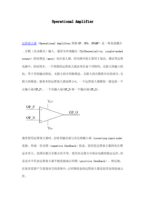
Operational Amplifier运算放大器(Operational Amplifier,简称OP、OPA、OPAMP)是一种直流耦合﹐差模(差动模式)输入、通常为单端输出(Differential-in,single-ended output)的高增益(gain)电压放大器,因为刚开始主要用于加法,乘法等运算电路中,因而得名。
一个理想的运算放大器必须具备下列特性:无限大的输入阻抗、等于零的输出阻抗、无限大的开回路增益、无限大的共模排斥比的部分、无限大的频宽。
最基本的运算放大器如图1-1。
一个运算放大器模组一般包括一个正输入端(OP_P)、一个负输入端(OP_N)和一个输出端(OP_O)。
通常使用运算放大器时,会将其输出端与其反相输入端(inverting input node)连接,形成一负反馈(negative feedback)组态。
原因是运算放大器的电压增益非常大,范围从数百至数万倍不等,使用负反馈方可保证电路的稳定运作。
但是这并不代表运算放大器不能连接成正回馈(positive feedback),相反地,在很多需要产生震荡讯号的系统中,正回馈组态的运算放大器是很常见的组成元件。
开环回路运算放大器如图1-2。
当一个理想运算放大器采用开回路的方式工作时,其输出与输入电压的关系式如下:Vout=(V+-V-)*Aog其中Aog代表运算放大器的开环回路差动增益(open-loop differential gai 由于运算放大器的开环回路增益非常高,因此就算输入端的差动讯号很小,仍然会让输出讯号「饱和」(saturation),导致非线性的失真出现。
因此运算放大器很少以开环回路出现在电路系统中,少数的例外是用运算放大器做比较器(comparator),比较器的输出通常为逻辑准位元的「0」与「1」。
闭环负反馈将运算放大器的反向输入端与输出端连接起来,放大器电路就处在负反馈组态的状况,此时通常可以将电路简单地称为闭环放大器。
LM741 UA741运算放大器使用说明及应用

LM741/UA741运算放大器使用说明及应用物理量的感测在一般应用中,经常使用各类传感器将位移、角度、压力、与流量等物理量转换为电流或电压信号,之后再由量测此电压电流信号间接推算出物理量变化,以达成感测、控制的目的。
但有时传感器所输出的电压电流信号可能非常微小,以致信号处理时难以察觉其间的变化,故需要以放大器进行信号放大以顺利测得电流电压信号,而放大器所能达成的工作不仅是放大信号而已,尚能应用于缓冲隔离、准位转换、阻抗匹配、以及将电压转换为电流或电流转换为电压等用途。
现今放大器种类繁多,一般仍以运算放大器(Operational Amplifier, Op Amp)应用较为广泛,本文即针对741运算放大器的使用加以说明。
1. 运算放大器简介ab126计算公式大全放大器最初被开发的目的是运用于类比计算器之运算电路,其内部为复杂的集成电路(Integrated Circuit, IC),亦即在单一电子组件中整合了许多晶体管与二极管,图1为一般放大器之内部等值电路。
1. 运算放大器内部等值电路图运算放大器属于使用反馈电路进行运算的高放大倍率型放大器,其放大倍率完全由外界组件所控制,透过外接电路或电阻的搭配,即可决定增益(即放大倍率)大小。
图2为运算放大器于电路中的表示符号,可看出其包含两个输入端,其中(+)端为非反相(Non-Inverting)端,而(-)端称为反相(Inverting)端,运算放大器的作动与此二输入端差值有关,此差值称为「差动输入」。
通常放大器的理想增益为无穷大,实际使用时亦往往相当高(可放大至105或106倍),故差动输入跟增益后输出比较起来几乎等于零。
838电子图2. 差动运算放大器表示符号2. 741运算放大器使用说明2.1 作动方式与原理新艺图库741放大器为运算放大器中最常被使用的一种,拥有反相向与非反相两输入端,由输入端输入欲被放大的电流或电压信号,经放大后由输出端输出。
美国临床医学工程师的考试大纲(译)

美国临床工程师的专业职责(译)作者:Thomas J. Bauld Ph.D.Chairman, Clinical Engineering Definition Committee, AmericanCollege of Clinical Engineering.原著:"The Definition of A Clinical Engineer", From: Journal of Clinical Engineering, V ol.16 5 , 1991.>随着科技的快速进步,也加速了医疗管理走向多专业领域的整合,临床工程学是根基于工程学与生命科学的一支也因应而蓬勃发展。
本文系美国临床工程学会所定义的『临床工程师』一词,提供读者更进一步了解这一新兴的医院新的专业角色。
一位临床工程师,他或她是应用工程专业与医疗性科技管理技术于支持与推展病人医疗照顾的专业人员。
一位临床工程师至少应具备经工程与技术评鉴委员会认可的学士资格,或具有工程师知识与技能考试合格的专业执业者。
临床工程师系一相当新的专业领域,在美国七0年代各大学院校才发展正式课程授予学士、硕士或博士的临床工程或生物医学工程学位,课程内容包括:物理学、生命科学、数学、人性科学、管理科学与工程科学,许多传统工程学是临床工程的基础,例如:电子工程、机械工程、化学工程与计算机工程等;生命科学课程通常包括:生物化学、生物学、生理学与解剖学等;工程学与生命科学的多专业组合而成的多重专业领域是临床工程与其它工程科学专业所不同的独具特色。
在临床工程的大学课程必须合乎进入医学预备课程的专业课程要求,再获取工程、商业管理、医疗管理或科技管理的较高学位;教育单位或专业团体或雇主则扮演提供临床工程师的持续教育训练角色。
虽然工程学位是主要的专业训练,但是有某些人他们的专业训练与知识经验累积造就与正式工程师相同的基础,尤其是早期临床工程未正式授予专业学位时,他们已具备临床工程师生命科学与工程物理科学知识者,美国国际证照委员会备有授予临床工程师的认定办法。
参考电压 英语
参考电压英语
参考电压英语:reference voltage。
例句:
1、参考电压产生单元用以提供多个电压电平。
The reference voltage generation unit provides a plurality of voltage levels.
2、电路基础是单运算放大器,其不需要参考电压。
The circuit's basis is a single operational amplifier, and it needs no reference voltages.
3、那是因为0 V的参考电压通常是指众所周知的大地。
That's because the 0 V reference is usually the famous ground.
4、在电压扰动期间使用递推算法计算每一时刻的参考电压。
During the voltage sag, the reference values are replaced by those which are calculated from the actual values according to the forecast algorithm.
5、提出一种采用改变参考电压来校正热电偶非线性的简单方法。
The simple method by changing reference voltage for non-linear correction of thermocouples is introduced.。
英汉电力技术词汇opq

observer errors 观察者误差
observing point 观测点
obsolete 已废的,不能用的
obsolete price 过期价格
obsolete project 过时项目
obstacle 阻碍,障碍[物];干扰;雷达目标
observation table 观测台,检查台
observation window 观察窗,视察窗
observatory 观测台,天文台
observe 遵守(法律)
observed 被观察的
observed data 观测数据,实验数据,被观察的数据
observed mean time 平均观察时间
occupational cancer 职业性癌
occupational chemical erosion 职业性化学侵蚀
occupational disease 职业病
occupational environment 职业环境
occupational exposure 职业性照射[量]
octal base 八脚管底
octal debugger 八进制调试程序
octal debugging technique 八进制排错法;八进制调试技术
octal digit 八进制数制,八进制数字
octal loading program 八进制装入程序,八进制调入程序
octal multiplication 八进制乘法
OA (overall) 总的,所有的
OAD (overall dimension) 总尺寸,外形轮廓尺寸
Operational Amplifiers

A First Look at OP-AMPS The term operational amplifier refers to a circuit that is composed of transistors, resistors, and capacitors, and that has a very large Thevenin input resistance and a very small Thevenin output resistance. It behaves, over at least a portion of its operating range, as a high-gain linear voltage amplifier.
These signs, however, are simply the names of the terminal and a pair of terminals to which dc voltages, called supply voltages, are connected. Batteries or regulated dc power supplies can be used; in either case, these voltage sources supply power to the components inside the op-amp and any power delivered to an output load.
Each terminal on an op-amp has a name. The conventionally used names for the two input terminals often confuse beginning students. The so-called inverting input is identified with a minus sign, and the non-inverting input with a plus sign.
Operational_Amplifiers(运放电路的生动介绍)

ME 6405 Introduction to Mechatronics
Basic Circuits Review
• Capacitance (Farad – F)
– Series
– Parallel
• Inductance (Henry – H)
– Series
– Parallel
ME 6405 Introduction to Mechatronics
ME 6405 Introduction to Mechatronics
High pass filter (active)
Band-pass filter cascades both high-pass and low-pass!
ME 6405 Introduction to Mechatronics
ME 6405 Introduction to Mechatronics
Filters
• Decouple the low-pass RC filter from the load.
Uses: Simple audio. Remove frequencies over 20kHz (audible)
Difference
Vout
V 2 R3 R1 R4 V1R3 ( R4 R2 ) R1 R1
If all resistors are equal:
Vout V2 V1
ME 6405 Introduction to Mechatronics
Integrating Op-Amp
ME 6405 Introduction to Mechatronics
Low-pass Filter (active)
运算放大器
RF uo ui 1 R1 RF (1 uo ) u R1
R3 RF (1 ) ui 2 R1 R2 R3
+ ui1 + ui2 R2 – –
R1
– u+ + + R3
+ uo –
uo uo uo
R3 RF RF (1 ) ui 2 ui 1 R1 R2 R3 R1
电工电子教学部
例:电路如下图所示,已知 R1= 10 k ,RF = 50 k 。 求:1. Auf 、R2 ; 2. 若 R1不变,要求Auf为 – 10,则RF 、 R2 应为 多少? RF
R1 R2 – + + 解:1. Auf = – RF R1 = –50 10 = –5 uo – +
+ uo –
RF R1 Ri1 Ri2
电工电子教学部
–
+
+
+ uo –
RF Ri 2 Ri 1 uo (1 )( ui 1 ui 2 ) R1 Ri 1 Ri 2 Ri 1 Ri 2
2、减法运算电路 RF + ui1 + ui2 R2 – – R1
– + + R3
常用做测量 分析方法1: 放大电路 由虚断可得: + uo –
电工电子教学部
三、集成电路器件命名及主要性能指标
国标 GB-3430-82 对集成电路的规定
第一部分 字 母 符号国标 符 号 C 意 义 符 号 T H E C F D W J B 第二部分 字 母 器件类型 意 义 TTL HTL ECL CMOS 线性放大 音响电视 稳压器 接口电路 非线性 第三 部分 数字 品种 符 号 C E R M 第四部分 字 母 工作条件 意 义 0 ~ 70C -40 ~ 85C -55 ~ 85C -55 ~125C 符 号 W B F D P J K T 第五部分 字 母 封 装 意 义 陶瓷扁平 塑料扁平 全封闭扁平 陶瓷直插 塑料直插 黑陶瓷直插 金属菱形 金属圆形
运算放大器知识

运算放大器最早被设计出来的目的是用来进行加、减、微分、积分的模擬数学运算,因此被称为“运算放大器”[1]。同时它也成为实现模拟计算机(analog computer)的基本建构单元。然而,理想运算放大器的在电路系统设计上的用途却远超过加减等的计算。今日的运算放大器,无论是使用晶体管(transistor)或真空管(vacuum tube)、分立式(discrete)元件或集成电路(integrated circuits)元件,运算放大器的效能都已经逐渐接近理想运算放大器的要求。最早期的运算放大器是使用真空管设计,现在则多半是集成电路式的元件,但是如果系统对于放大器的需求超出集成电路放大器的能力时,也会利用分立式元件来实现这些特殊规格的运算放大器。
运算放大器(英语:Operational Amplifier,简称OP、OPA、OPAMP、运放)是一种直流耦合,差模(差动模式)输入、通常为单端输出(Differential-in, single-ended output)的高增益(gain)电压放大器,因为刚开始主要用于加法,减法等模擬运算电路中,因而得名。
1968年:飞兆半导体公司推出 μA741,与 LM101 相比,μA741内部增加了30pF的频率补偿电容。该产品第二来源众多,迄今仍然在生产使用,它是有史以来最成功的运算放大器,也是极少数最长寿的IC型号之一;
1970年:开始出现输入端使用 FET 的高速、低输入电流(高输入阻抗)运算放大器;
目前运算放大器广泛应用于家电,工业以及科学仪器领域。一般用途的集成电路运算放大器售价不到一美元,而现在运算放大器的设计已经非常成熟,输出端可以直接短路到系统的接地端(ground)而不至于产生短路电流(short-circuit current)破坏元件本身。
运放的共模

运放的共模标题:深入探究运放的共模特性简介:本文将介绍运放的共模特性,分析其原理和应用,帮助读者更好地理解和应用运放。
正文:运放(Operational Amplifier,简称Op Amp)作为一种重要的电子元件,具有广泛的应用范围。
在实际应用中,我们不仅需要了解运放的基本特性,还需要深入研究其共模特性。
共模是指运放输入端同时接受到的共同模式信号。
运放的共模增益是衡量其共模特性的重要指标之一。
共模增益反映了运放在接收共模信号时的放大倍数。
如果运放的共模增益不理想,会导致信号失真,降低系统性能。
为了减小共模增益,提高运放的共模抑制比,我们可以采取一些措施。
首先,选择具有较高共模抑制比的运放器件。
其次,合理设计电路布局,减少共模信号的干扰。
此外,对于特殊应用场景,如在高噪声环境下工作,还可以采用差分输入运放,以提高系统的共模抑制能力。
除了共模增益外,共模偏移也是运放共模特性的重要指标之一。
共模偏移是指运放在输入端口所引入的偏移电压。
偏移电压会导致输出信号出现误差,影响系统的准确性。
为了减小共模偏移,我们可以采取校准电路、温度补偿等方法。
运放的共模特性不仅在模拟电路设计中起到重要作用,也在许多数字电路中有着广泛的应用。
例如,对于差分信号的接收和传输,我们经常使用差分运放来提高共模抑制能力,减小共模噪声的影响。
总之,了解和掌握运放的共模特性对于电子工程师来说至关重要。
通过深入研究运放的共模特性,我们可以更好地应用运放,提高系统的性能和稳定性。
在实践中,我们需要根据具体应用场景选择合适的运放器件,并合理设计电路布局,以减小共模干扰,提高系统的共模抑制能力。
通过持续学习和实践,我们可以不断提升对于运放共模特性的理解和应用能力。
集成运放实验报告
集成运放实验报告
一、实验内容
本次实验有两个目的:
1、学习集成运放器(Integrated Operational Amplifier)原理及其基本特性。
2、实现4级级联放大器,实验者要求将放大后的信号接到音箱上,在视觉上调节输入信号的大小,而无需任何外部仪器及辅助电路的情况下实现对输出信号的控制。
二、实验准备
实验前先查阅及准备一些基础理论,以利于理解操作过程中的变化,将电路图画出,清楚的理解其行为,熟悉试验电路并熟悉每个元件的性质,在此基础上检查实验准备是否齐全。
三、实验步骤
(1)先了解集成运放器原理,清楚其位移放大电路,了解集成运放器的基本特性,它可以实现大范围放大信号。
(2)根据目标功能,搭建实验电路,采取四级级联放大,运用集成运放器达到放大信号的目的,然后将输出信号接到音箱上,利用变阻器调节放大器的输入信号等级。
(3)最后,连接对应的电源线,查看设备运行是否正常,检查线路有无漏电,有无错接的线路,,如果没有可以放心使用。
四、实验结果
本次实验中,级联放大器把电路中的输入信号放大到输出信号,可以大幅度调节输出信号的等级,而无需任何外部仪器及辅助电路,测试结果证明级联放大器确实达到了预期的电路效果,实现了输出信号的控制以及增益的调节。
五、总结
通过本次实验,实现了无外接仪器就可以大幅度改变输出信号强度的级联放大器,掌握了常用集成运放器,以及其优势与功能,增进对运放器及其原理的理解。
- 1、下载文档前请自行甄别文档内容的完整性,平台不提供额外的编辑、内容补充、找答案等附加服务。
- 2、"仅部分预览"的文档,不可在线预览部分如存在完整性等问题,可反馈申请退款(可完整预览的文档不适用该条件!)。
- 3、如文档侵犯您的权益,请联系客服反馈,我们会尽快为您处理(人工客服工作时间:9:00-18:30)。
OPERATIONAL AMPLIFIER BASICSby Harry LythallIntroductionThe Operational Amplifier (Op-Amp) was developed many years ago for analogue computing. This was in the days when the output information from a calculation was readable with a simple voltmeter. Fortunately for us, the Op-Amp can be misused for a huge variety of functions. In this page I will attempt to show what the Op-Amp is and a few uses of it.What IS An Op-Amp?Basically, the Op-Amp is nothing more than a differential amplifier that amplifies the difference between two inputs. One input has a positive effect on the output signal, the other input has a negative effect on the output. The component circuit symbol is:For clarity, the power supply terminals to the amplifier chip are not usually shown, except on detailled circuit diagrams. The Op-Amp requires two power supplies; a positive voltage supply and a negative voltage supply, both with respect to our circuit ground/Earth/chassis connection.The theoretically perfect Op-Amp has an infinite voltage gain, an infinite bandwidth and infinite input impedances. In this way it just senses an input voltage level without actually interfering with that voltage in any way. The perfect Op-Amp also has a zero-Ohm output impedance. It may therefore be used to drive heavy (in electronic terms) circuits.A Practical Op-AmpThe practical Op-Amp is far from perfect, but the more you pay then the better the Op-Amp you get. The circuits I will give you in this article can all be built and used using the LM741 Op-Amp. Here you can find the datasheets for operational amplifiers, and other circuits, if you want a little extra reading. These chips look something like this:A typical operational amplifier has input impedances of 100M-ohms, 1-ohm output impedance and will drive up to 20mA of output current. Supply voltages may be as high as +20V and -20V (total 40 volts from +ve supply to -ve supply). The typical voltage gain/bandwidth of a normal Op-Amp is about 1 000 000. This is to say that at DC it will have a voltage gain of one Million, but at 1MHz it will only have a voltage gain of 1.To understand a little more of what is inside the chip, here is a much simplified circuit diagram.The circuit will function quite well with the component values shown, should you feel the need to built the device. In the real Op-Amp, the silicon diode biasing and current limiting resistors are constant current supplies that enable the device to operate at low supply voltages.Now you have a little information about what the device is, let us take a look at what it can do.Basic FunctionThe basic function of the Op-Amp is to multiply a voltage level by the gain of the amplifier. If you were to couple a DC level of +1v into the + input of our Op-Amp then the output would be 1v X 1000000 or one Million volts. The output, however, cannot exceed the supply voltage, so the output will be +20v DC.If you were to couple a DC level of +1v into the - input of our Op-Amp then the output would be -1v X 1000000 or MINUS one Million volts. The output, however, still cannot exceed the supply voltage, so the output will be -20v DC.If you were to couple a DC level of +1v into both the - and + inputs of our Op-Amp then the output would be (-1v X 1000000) plus (1v X 1000000) = 0v.In other words, both inputs act on the output simultaneously and the output is the sum of both input functions. If both inputs are identical then the output should always be zero. This is a good test for an Op-Amp. If you connected both inputs to the same input, then the output SHOULD be zero volts. In reality, there are small differences in the circuit's characteristics and components, this will result in a small "offset" voltage.The numbers beside the Op-Amp symbol are the chip pin numbers for the LM741.The offset voltage can be corrected on several Op-Amps by an internal circuits known as "offset null" which means that the offset voltage can be trimmed out.In most Op-Amp applications this function is not necessary, but in very accurate systems, such as instrumentation, the function can be very useful.The Op-Amp As A Comparator - LogicOne of the most basic Op-Amp functions is the voltage comparator. Here the two inputs are used to compare two different voltages. If the input to the + input is greater than the input to the - input then the output will be 1000000 times the difference between the two inputs.Example, if the + input were +3.2vDC and the - input were +3.215vDC then the output voltage will be 1000000 X the difference between the two inputs, or 1000000 X -0.015vDC = -15000vDC. Again, the amplifier cannot output a voltage beyond the supply voltages so the output will become -20vDC.Wow! This opens up a few possibilities. The gain is so high that the output can never be practically anything else but -20vDC or +20vDC. This is a good input circuit to CMOS and other digital equipment. Just change the supply voltages to match. It can also interface directly to an RS232 computer input if the supply were just + & - 10vDC. RS232 requires a 20mA current limit capability, so the 741 Op-Amp is ideal. The Hamcomm interface uses just this effect to interface an analogue signal to the computer so radio amateurs can interface a radio receiver to the PC.The basic voltage comparator can also have many other uses, for example, as a battery under/over voltage indicator.Here, the input voltage to your precious VHF transciever can be monitored by a simple device to give you an idea as to the battery condition. The 13.8vDC input is regulated by a Zener diode (6.8v works fine) and the resultant 6.8vDC is then presented to the -ve input of the Op-Amp. This will drive the Op-Amp output to the -ve supply voltage, which in this case is ground (0v). The input voltage is also divided by a 50K preset potentiometer and fed into the + input of the same Op-Amp. As long as the 50K preset delivers more than 6.8vDC then the output of the Op-Amp will be high and equal to (almost) the 13.8vDC input. If you want to reverse the sense of the device then just reverse the + and - input to the Op-Amp.The DC output from the 50K preset potentiometer will vary in sympathy with the 13.8vDC input to the whole circuit. The DC voltage across the Zener diode, however, will be a constant, quite independant on the input voltage. Assume the 50K preset is set to mid-position then the pot will deliver 13.8/2 = 6.9v to the Op-Amp + input. The Op-Amp will therefore always deliver a high voltage from it's output and the LED will be illuminated. If the input fell below 13.6vDC then the preset will deliver less than 6.8v to the Op-Amp and the Op-Amp output will change from High (13.8v) to Low (0v). A voltage warning indicator.The Op-Amp comparator can also be used in many other applications where voltages vary, for example, the basic CR time-constant circuit. In this example, I have chosen to make a simple timer circuit.When the switch S is pressed and released, the capacitor C will discharge, then begin to charge through R. The voltage across C will start at 0v, so the output from the Op-Amp is also Low (0v). As soon as the capacitor charge rises to more than 6.8v then the + input to the Op-Amp is greater than the - input and the Op-Amp output will suddenly switch High (12v) and the LED will light. In this circuit you may, of course, replace the 470R and LED for a small relay. Any relay capable of switching from just 20mA will do the job.Ok then, so now you know all about using the Op-Amp as a voltage comparator and some of the ways it could be used. It is probably time to start using the Op-Amp in some analogue circuits.The Op-Amp As A Comparator - AnalogueThe basic Op-Amp gain is for too high to be of much use in analogue circuits without some form of control. That form of control usually comes in the form of "negative feedback". This means simply connecting all, or a part, of the Op-Amp output back to the - input.Here we see that pin 6 of the Op-Amp is coupled directly back to pin 2, so that 100% of the output voltage is coupled back to the - input of the Op-Amp. Now we have applied 100% negative feedback. If any voltage is applied to the + input (pin 3) then the Op-Amp will only become stable if the output voltage is the same. If the output is too high then - input is higher than + input and the output will fall. If the output is too low then - input is lower than + input and the output will rise. The only stable condition that can exist is if the + and - inputs are the same voltage.If you now vary the 50K potentiometer then the Op-Amp output will follow the input voltage from the pot. The advantage here is that any load placed on the Op-Amp will not affect the voltage since the Op-Amp controls it. Any error will be fed back in the opposite polarity and cause a correction. This circuit is a simple low current (20mA) variable voltage generator. You can increase the output current capability by adding a transistor for the Op-Amp to drive.Here we have added a single transistor buffer stage. If the Hfe of the transistor was 100 and the Op-Amp can deliver up to 20mA, then this PSU circuit would handle up to 2-Amperes. Naturally, the transistor should be fitted to a heatsink and should be capable of handling that sort of load current. You will also see that I have taken the liberty of taking the reference voltage from a Zener diode. Now our power supply unit will be as well regulated as the Zener diode.The power transistor will drop 0.7v between Base and Emitter (1.4v for a power Darlington transistor) which would otherwise lower the output voltage of the complete PSU. I have connected the - input of the Op-Amp, not to the Op-Amp output, but to the output of the regulator transistor. The circuit functions exactly as before, but the result of the 100% negative feedback will be to maintain the output of the transistor TR at the correct voltage. The output of the Op-Amp may be a volt or two higher than this; whatever is needed to control the transistor.In reality, this circuit would be a little dangerous to use withou some form of current limiting, but that is outside the scope of this article. There are circuits elsewhere on my homepages.One other small point, all devices generate noise. The Op-Amp is no exception, but in the above circuit the negative feedback will remove all traces of noise from the output of the PSU that are generated WITHIN THE FEEDBACK LOOP. The 50K pot and Zener diode lie outside the feedback loop. The 50K pot will not generate much noise, but the Zener diode is a very noisy device. It should be decoupled with a large electrolytic capacitor.Another point here is temperature stability. A 15v zener diode will have a voltage variation of about 25mV for every degree Centegrade. A 10 degree rise in temp will therefore cause the full-voltage output from the PSU to vary by 1/4 of a volt! To overcome this we can modify the circuit to use the gain of the Op-Amp. We know that high-voltage Zener diodes have a +ve temperature coefficient and low-voltage Zeners have a -ve coefficient. A 5.6v Zener has a temperature coefficient of about 0v per degree centigrade. So let us substitute the 15v Zener with a 5.6v Zener. Now let us modify the circuit so we can still have a 0-15v variable PSU.All I have added is R1 and R2 which form a voltage divider. The feedback loop now has a bit of gain, equal to (R1 + R2) / R2 which is a gain of only 2.7857. The reference can now vary from 0 to 5.6v and the maximum voltage available is 5.6v X 2.7857 = 15v (welllll..... 15.6v ... maybe a little over, but who cares?).If the Zener generates 5.6v and the voltage pot is set to maximum, then the + input of the Op-Amp is +5.6v. This will drive the output of the Op-Amp high, until the - input of the Op-Amp (pin 2) is also 5.6v. Pin 2 is connected to the junction of R1 and R2 and this can only become 5.6v if the right-hand side of R1 is 15.6vDC. Our PSU now works and has a very good temperature stability.Audio AmplifiersThe Op-Amp makes an ideal audio amplifier with very few external components. With an output current of up to 20mA then it can also drive headphones and even high-impedance speakers, eg. 50 - 80 ohms. To use the Op-Amp for linear (undistorted) audio applications we always need to use negative feedback. It is the negative feedback that "tames the wild beast". With an "open loop" voltage gain of over 1000000 times then we do need to "tame" the amplifier.R1 and R2 again control the voltage gain of the amplifier and the gain is equal to (R1 + R2) / R2 and the gain may be set to anything practical within the scope of the Op-Amp. Bear in mind the gain/bandwidth characteristic of the Op-Amp. If you wanted the amplifier to have a flat response from 0 - 20KHz and the Op-Amp gain/bandwidth was 1000000, then at 20KHz the open loop amplifier gain cannot be greater than 1000000/20000 = 50. If you wanted a flat response from 0 - 20KHz with a gain of 200 then you should use two amplifiers with a total voltage gain product of 200. Audio test signals through the amplifier should be sinusoidal, something like this:The amplifier shown has a frequency response of 0Hz to "somethingquitehigh" and is limited only by the Op-Amp gain/bandwidth characteristic. The input resistor Rin can be typically 1M0 and just references the + input to ground (0v). If you wanted a specific input impedance then change Rin to suit the input impedance you want. In real life you would also want to isolate the input and output from any DC component. This would be done with capacitors:The reactance of the capacitors should be at least 0.2 x the input or output impedances at the lowest operating frequency. For example, Rin = 50K and the lowest frequency we wish to amplify is 20Hz, then the reactance of C1 shall be 10K at 20Hz, which would be about 0.8uf. If the output were driving a 72-ohm headphone then C2 reactance shall be 14.4-Ohms at 20Hz, or about 560uf.This amplifier would be quite fine if you had both + and - 20v DC supplies, but in most applications we are not so fortunate. To modify the circuit to operate from a single supply, we have to move the amplifier DC operating point away from 0v to something else. Add a couple of 1K0 series resistors to divide the single supply voltage. If we had a single supply of +20 volts available, then the new operating point would be 1/2 of that = 10vDC.Naturally, the two 1K0 resistors shall be decoupled to remove any trace of audio ripple, using a BIG electrolytic capacitor. The reactance of the capacitor shall be 0.2 x R2 at the lowest operating frequency. If the two 1K0 resistors were NOT identical then the amplifier would distort at high signal levels:All the coupling and decoupling caps values discussed so-far are MINIMUM values. If the capacitors are larger then the AC characteristics of the amplifier will only improve a little. If they are too large then it may take a few seconds (or minutes) for the amplifier to stabilise when you switch ON the power.The AF amplifiers discussed so-far have the input signal fed into the + input which means that the output signal is in the same phase as the input signal. But what if we want the signal to be inverted? Easy, change the original configuration to feed the input signal into the -ve input:In this event the input resistor Rin that sets the input impedance is also the R2 feedback resistor. The gain of the stage will also be reduced by 1. The voltage gain is now R2/R1 which means that an amplifier voltage gain of less than 1 is now possible.Another usefull point with this circuit, the output and inputs are 100% out of phase. The + input is referenced to 0v (ground) and so the -ve input MUST also be 0v. There will also be NO SIGNAL at the - input pin. This point in this circuit is called a "Virtual Earth".Audio Power AmplifiersPower = Volts X Amperes. So to get an AF power amplifier we must have both volts and current. We have already seen how to build a voltage amplifier, now let us give it a little current capability. We can do this by simply adding a pair of power transistors, one to give positive current, the other to give negative current.It is quite simple and this particular amplifier will deliver over20-watts RMS (40-watts Music Power) into a 6-Ohm speaker. It will sound like crap, but at least the power is there (great for RAP music!). Notice how R1 has been moved. In this way the distortion generated by the power transistors will be fed back to generate an "anti-distortion" signal at the output of the Op-Amp. If the voltage gain of the amplifier is set quite low, for example X10 maximum, then the sound of this circuits is quite acceptable. But if you put your head inside the speaker, or increase the gain, then you will hear a very unpleasant distortion at low volume levels. This distortion is called "crossover distortion" and is caused by the transistors not conducting until the signal level has exceeded 0.7vDC. It looks like this on an oscilloscope:The cure, of course, is to make the transistors conduct a little current when they are idle. The simplest form of conduction bias would be to add resistors and diodes.The resistor R+ and D1 provide a bit of current into the base of the NPN transistor. D1 ensures that the DC voltage is the output of the Op-Amp plus 0.7v. R- and D2 do the same at the opposite side for the PNP transistor.Audio Amplifier LimitationsLet us go back to our basic Op-Amp AF amplifier for a few moments, both the circuit and all the internal "gubbins":andRemember that the Op-Amp may operate from as little as 5v and as high as 40 volts. This gives rise to some form of design conflicts, at least with the cheaper Op-Amp chips. At low signal levels they can distort; crossover distortion generated within the chip. If you want an output signal of, say, +/-10v then there may be no problem at all, but a small high-gain pre-amplifier with an output in the region of 0.1v RMS could suffer terrible crossover distortion. The "cure" for this is to either reduce the gain and/or add a bit of bias current to the output stage.I have now added Rbias which makes one of the output transistors (BC557) conduct permanently. This effectively converts the output stage to a single transistor Class-A amplifer, the other (NPN) transistor never being used.If you do not wish to muck about with transistors in conjunction with an Op-Amp then choose a "Power Op-Amp" such as the LM2020 which already has the power transistors built-in. This Op-Amp will provide 20 watts of audio. You can even use it to drive motors and lamps. This amplifier must be mounted on a heatsink.Frequency ResponseNow you know what an Op-Amp is all about and how it can be used to make amplifiers, let us consider the limitations of frequency response. I have already introduced the concept of "Unity Gain/Bandwidth" (UGB). So let us explore this a little more.Imagine for one moment that an Op-Amp had a Unity Gain/Bandwidth of 1000000Hz and we used resistors to set the amplifier voltage gain to 190 and then 20. What would the actual frequency response be? This graph shows you exactly what will happen.With a voltage gain of 190 set, the amplifier will have a gain of 190, but ONLY up to that frequency where the open-loop gain of the Op-Amp reduces to 190. That point would occur at about 6KHz. Not very good for Hi-Fi reproduction! But if we were to reduce the voltage gain to just 20 then the frequency response would extend to 50KHz. If we needed an amplifier to have a gain of 190 then we would be far better off to have two cascaded amplifier; each with a voltage gain of just 14. The total gain would then be a little over 190 and the frequency response would be DC to over 70KHz.Frequency ResponseBut is UGB the end of the limitations story? No! Operational amplifiers have another property called "Slew Rate". This means that if the input waveform were to be a square-wave then the output would not change instantaneously. It would take a finite time for the output to change state.If this slope were shallower than a part of our signal then the signal waveform will distort. If the same waveform were reduced in amplitude then the signal slope would also reduce. This means that the Op-Amp's "slew rate" would affect high-level signals more than low-level signals. Consider the following two output sine-waves with respect to the slew-rate (shown in RED).In the first waveform, the signal amplitude is high, so the slope is steep; steeper than the slew rate of the Op-Amp can follow. The waveform will therefore become distorted. The second waveform is of exactly the same frequency, but the signal amplitude is low. The slope of the waveform is therefore less steep than the slew rate of the Op-Amp, so the waveform will be undistorted.In reality, the Slew rate characteristic of an Op-Amp will only affect signals of a very high frequency, or waveforms having a very steep rise and fall time, for example, square and sawtooth waveforms. For general audio work up to about 30KHz you can normally forget about this effect. The slew rate of an Op-Amp may complicate matters if you try to drive fast logic circuits, such as the 5400 and 7400 series. If you need to drive TTL circuits from Op-Amps then try to choose a logic gate that has a "Schmitt" input function. CMOS gates tend to be a bit more forgiving so you can usually get away with driving them directly from Op-Amps.Active Low-Pass FilterThe high input impedance of the Op-Amp makes it especially usefull in filter design. Simple RC filters are good, but in order to take an output signal from them you need to load the filter. It is the load that "cocks up" everything. Your load circuit may be resistive, that will affect the responses of the filter. If your load is capacitive or inductive then you have little chance of predicting the outcome with any form of accuracy. So, let us consider the basic Low-Pass filter:At the frequency of calculation, the output signal will have fallen by 50% of the voltage, or -6dB if you prefer decibels. If you double the frequency then it will have fallen by another 50% (now 25%). Another usefull reference point is the output signal falls by a further 90% every frequency decade. To all intents and purposes, the loss of the filter is zero at F/2. The filter has no gain, in fact, any load at all will cause it to have a loss at all frequencies. This is what we are going to cure first.( or to be more conventional )The Op-Amp has simply become a high-impedance buffer stage and has also given the filter a little gain by virtue of (R1+R2)/R2, or R/Rgain in the more conventional circuit. The output impedance is almost zero ohms.The Op-Amp really "earns it's corn" when you want a little more that 6dB/octave (20dB/decade) rolloff. You could simply cascade twosingle-pole filters, but inacuracies can enter when one filter is a load for the next. This filter is a 2-pole filter having a rolloff of12dB/octave (40dB/decade), which in real terms is 25% of the original signal level:Notice that the turnover formula has changed a little. The 6dB point has now become a 12dB point; the new 6dB point is somewhat lower in frequency, so the 1 in the top line of the formula has become 0.7071 instead. This filter gives a unity gain up to the point it begins to "turnover" - about 0.5/(2 pi R C)Active High-Pass FilterThe active high-pass filter is almost the same as the low-pass, but the C and R are exchanged in the circuit to give the opposite response curve. First, the basic high-pass circuit element.Again, the turnover frequency for the single-pole filter is 1/(2PiCR) and now we shall buffer it with the Op-Amp.The basic response is still 6dB per octave (20dB per decade) which may not be too usefull for general work. To all intents and purposes, the response is flat from 2/(2PiRC) upwards. Adding an extra RC circuit to make a 2-pole filter will increase the rolloff slope to 12dB per octave.The The losses at 1/(2PiCR) have now increased from -6dB to -12dB so the rolloff point is now 1.41/(2PiRC). I must state here that this only applies for a unity voltage gain (1). To get other voltage gains complicates the formula and they can become quite complex.Active Band-Pass FilterThis is easy. Use a Low-Pass AND a High-Pass in cascade.Active Rejection FilterIn many application you need to pass a complete band but with a filter to reject just one single frequency. There are many circuits for this, but here is one that I find so simple that even I understand it and I can remember the formula!The notch frequency is 1/(2PiRC). The "Gyrator" circuit uses two Op-Amps in a novel circuit where one amplifier inverts the effects of a capacitor which then behaves as an inductor. But I think this has now gone beyond the scope of an article on Op-Amps. But here is the circuit, anyway.This is one of the circuits that remains firmly planted in my memory, but the brain-failure has extended to the formulas - Sorry! The roughorder-of-magnitude is that R is 10K and C is 10nf for somewhere in the middle of the AF band, probably about 1.5KHz. This would imply that1/(2PiRC) would be the formula, but don't quote me on that. The resistor Q would be about 100K for a bandwidth in the region of about 10Hz or so. Gain is 1 although the output impedance from Out1 is quite high, so an Op-Amp buffer would be needed here.ReferencesThis is about all I wish to write on this subject. If you are interested in further reading then I suggest you take a trip to your local library. There are several educational Op-Amp books that you may find of interest:The ARRL Handbook For Radio Amateurs is rather good and easy to understand, but it is a little rudimentary. Assuming you know nothing, you assimilate all the Op-Amp section in one "sitting" on the toilet.Electronic Circuits (Discrete and integrated)Donald L. Schilling & Charles Belove published by McGraw-Hill International is a real goldmine but tends to be a little "heavy" when it comes to mathematics - I keep my copy in the toilet so I am never short of reading material.The IC OP-AMP Cookbook" is published by Sams & simply OP-AMPS published by Newnes press are both well worth reading. They contain a lot of useful information for all levels of knowledge. If you seriously wish to learn more, or have an Op-Amp reference data handy, then these are the books for you.If you want an on-line resource for active filters then you could visit /filters/active-bandpass-filters. htm or /active.html where you will find loads of information, although a lot of it is designed to sell filter design software.Best regards from Harry Lythall - SM0VPO, Lunda, SwedenReturn to INFO page。
