12104D107MAT2A中文资料
AD2S1210芯片手册-中文

One Technology Way, P.O. Box 9106, Norwood, MA 02062-9106, U.S.A.Tel: 781.329.4700 Fax: 781.461.3113 ©2008–2010 Analog Devices, Inc. All rights reserved.功能框图REFERENCE OSCILLATOR(DAC)EXCITATION OUTPUTSAD2S1210E N C O D E R E M U L A T I O NSYNTHETIC REFERENCE RESETDATA I/OINPUTS FROM RESOLVERENCODER EMULATION OUTPUTSVOLTAGE REFERENCEREFERENCEPINSINTERNAL CLOCK GENERATORCRYSTALTYPE IITRACKING LOOP FAULT DETECTIONFAULTDETECTION OUTPUTSPOSITION REGISTERADCADCCONFIGURATIONREGISTERMULTIPLEXERDATA BUS OUTPUTDATA I/OVELOCITY REGISTER07467-001图1.AD2S1210分辨率可变、10位至16位R/D转换器,内置参考振荡器产品特性完整的单芯片旋变数字转换器最大跟踪速率:3125 rps(10位分辨率) 精度:±2.5弧分分辨率:10/12/14/16位,由用户设置 并行和串行10位至16位数据端口 绝对位置与速度输出 系统故障检测可编程故障检测阈值 差分输入增量式编码器仿真内置可编程正弦波振荡器 兼容DSP 和SPI 接口标准电源电压:5 V ,逻辑接口电压2.3 V 至5 V 额定温度范围:−40°C 至+125°C应用直流和交流伺服电机控制 编码器仿真 电动助力转向 电动汽车集成的启动发电机/交流发电机 汽车运动检测与控制概述AD2S1210是一款10位至16位分辨率旋变数字转换器,集成片上可编程正弦波振荡器,为旋变器提供正弦波激励。
UN1210中文资料
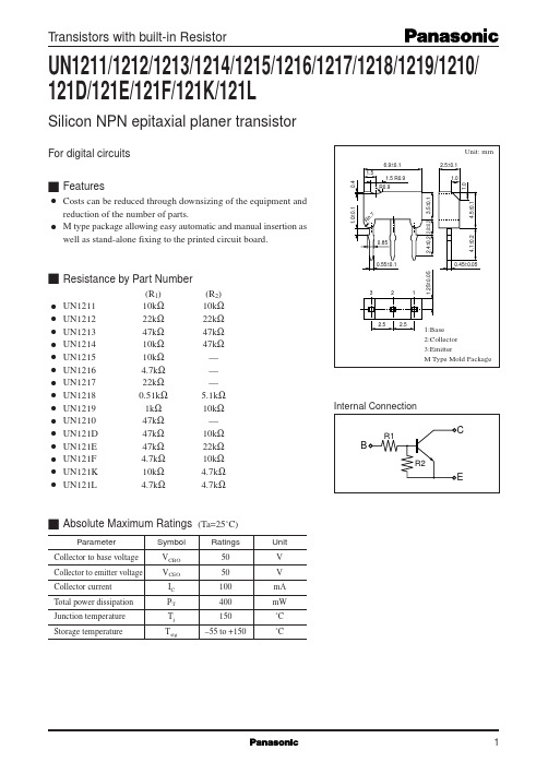
3.5±0.1
1.0 2.4±0.2 2.0±0.2
0.45±0.05 2 1 2.5
1.0±0.1
R 0. 7
0.85
0.55±0.1
s Resistance by Part Number
q q q q q q q q q q q q q q q
UN1211 UN1212 UN1213 UN1214 UN1215 UN1216 UN1217 UN1218 UN1219 UN1210 UN121D UN121E UN121F UN121K UN121L
120 100 80 60
0.7mA 0.6mA 0.5mA 0.4mA 0.3mA
Forward current transfer ratio hFE
Collector current IC (mA)
300 Ta=75˚C
200 25˚C 100 –25˚C
0.2mA 40 20 0 0 2 4 6 8 10 12
3
2.5
1:Base 2:Collector 3:Emitter M Type Mold Package
Internal Connection
R1
1.25±0.05
C
B
R2
E
s Absolute Maximum Ratings
Parameter Collector to base voltage Collector to emitter voltage Collector current Total power dissipation Junction temperature Storage temperature Symbol VCBO VCEO IC PT Tj Tstg
TMCM-1210 硬件手册说明书

TRINAMIC Motion Control GmbH & Co. KGHamburg, GermanyHardware Version V 1.10HARDWARE MANUAL+ +TMCM-12101-Axis steppercontroller/drivermax. 0.6A RMS / 24V DC STOP / HOME switch input hall sensorRS485++Table of contents1Life support policy (3)2Features (4)3Order codes (5)4Mechanical and Electrical Interfacing (6)4.1Dimensions and Mounting Holes (6)4.2Board mounting considerations (6)4.3Connectors (7)4.3.1Power, RS485 + HOME connector (8)4.3.2Motor connector (9)4.4Power supply (9)4.5RS485 (10)5Motor driver current (12)6On-Board LEDs (13)7Reset to Factory Default Values (13)8EMC considerations (14)9Operational Ratings (15)10Functional Description (16)11Revision History (17)11.1Document revision (17)11.2Hardware revision (17)12References (17)1Life support policyTRINAMIC Motion Control GmbH & Co. KG does not authorize or warrant any of its products for use in life support systems, without the specific written consent of TRINAMIC Motion Control GmbH & Co. KG.Life support systems are equipment intended to support or sustain life, and whose failure to perform, when properly used in accordance with instructions provided, can be reasonably expected to result in personal injury or death.© TRINAMIC Motion Control GmbH & Co. KG 2015 - 2019Information given in this data sheet is believed to be accurate and reliable. However neither responsibility is assumed for the consequences of its use nor for any infringement of patents or other rights of third parties, which may result from its use.Specifications are subject to change without notice.2FeaturesThe TMCM-1210 is a highly compact 20mm x 20mm single axis stepper motor controller and driver board with RS485 interface. It has been designed in order to be mounted on the rear side of a NEMA8 (20mm flange size) stepper motor and offers an integrated hall-sensor based encoder IC in addition to a reference switch input for easy homing / search of reference position. The module supports motor currents up to 0.6A RMS and supply voltages up to 24V DC nominal. It is available with standard TMCL firmware and supports stand-alone operation (TMCL programs with auto-start stored on-board) and remote control via RS485 interface.MAIN CHARACTERISTICSMotion controller∙Motion profile calculation in hardware in real-time∙Motion controller supports linear and sixPoint™ ramps∙On the fly alteration of motor parameters (e.g. position, velocity, acceleration)∙High performance microcontroller (Cortex-M0+) for overall system control and serial communication protocol handlingBipolar stepper motor driver∙Up to 256 microsteps per full step∙Highly integrated and highly-efficient operation∙Dynamic current control∙stallGuard2™ feature for stall detectionInterfaces∙RS485 2-wire communication interface∙Digital input IN0 (+24V compatible), can be used as reference switch or left and/or right stop switch input, alsoOn board hall sensor∙Absolute sensor within one motor rotation∙12bit / 4096 steps / revolution max.∙Low-cost sensor - suitable for low velocity applications (few hundred rpm) –e.g. initial reference search (together with HOME sensor input) after power-upSoftware∙TMCL™ remote (direct mode) and standalone oper ation with memory for up to 876 TMCL commands∙Fully supported by TMCL-IDE (PC based integrated development environment)Electrical data∙Supply voltage: +7V… +30V DC∙Motor current: up to 0.6A RMS (programmable)Mechanical data∙Board size: 20mm x 20mm, overall height 9mm max. (without mating connectors and cables)∙Mounting holes compatible with NEMA 8 stepper motors (for mounting the board to the rear side of a NEMA8 stepper motor using two of the four existing screw)Please see separate TMCM-1210 Firmware Manual for additional information regarding firmware functionality and TMCL programming.3Order codesThe TMCM-1210 is available as:A cable loom set is available for this module, also:Table 3.2: Cable loom order code4 Mechanical and Electrical Interfacing4.1 Dimensions and Mounting HolesThe dimensions of the board are approx. 20mm x 20mm x 9 mm in order to fit on the back side of a 20mm (NEMA8) stepper motor. Maximum component height (height above PCB level) without mating connectors is around 6mm above PCB level and 2 mm below PCB level. There are two mounting holes for M2 screws for mounting to a NEMA8 stepper motor.2xFigure 4.1 Dimensions of TMCM-1210 and position of mounting holes (with comparison of size)4.2 Board mounting considerationsThe TMCM-1210 offers two metal plated mounting holes. Both mounting holes are connected to power supply ground. Please keep this in mind when mounting the board to the rear side of a motor.Figure 4.2: Example of TMCM-1210 mounted to NEMA 8 stepper motor4.3 ConnectorsThe TMCM-1210 offers two connectors including the motor connector which is used for attaching the motor coils to the electronics. The Power, RS485 and HOME connector is used for power supply, RS485 serial wire communication and offers one digital input.4115Power, RS485 + HOME connector HOME 5RS485+RS485-34VDD GND 12IN0STOP_L / STOP_R Motor connectorOA1OA234OB1OB212Figure 4.2 Overview connectorsOverview of connectors and mating connectors types:Table 4.1: Connectors and mating connectors, contacts and applicable wire4.3.1Power, RS485 + HOME connectorThe module offers one combined power, RS485 2-wire serial communication and digital input (HOME) connector (JST PH series).51Table 4.2: Power, RS485 + IN0 connector4.3.2 Motor connectorAs motor connector a 4pin JST PH-series 2mm pitch single row connector is available. The motor connector is used for connecting the four motor wires of the two motor coils of the bipolar stepper motor to the electronics. 14Table 4.4: Motor connector 4.4 Power supplyFor proper operation care has to be taken with regard to power supply concept and design. Due to space restrictions the TMCM-1210 includes just about 20µF/35V of supply filter capacitors. These are ceramic capacitors which have been selected for high reliability and long life time.4.5RS485For remote control and communication with a host system the TMCM-1210 provides a two wire RS485 bus interface. For proper operation the following items should be taken into account when setting up an RS485 network:1.BUS STRUCTURE:The network topology should follow a bus structure as closely as possible. That is, the connection between each node and the bus itself should be as short as possible. Basically, it should be short compared to the length of the bus.termination resistor (120 Ohm)termination resistor (120 Ohm)Figure 4.6: Bus structure2.BUS TERMINATION:Especially for longer busses and/or multiple nodes connected to the bus and/or high communication speeds, the bus should be properly terminated at both ends. The TMCM-1210 does not integrate any termination resistor. Therefore, 120 Ohm termination resistors at both ends of the bus have to be added externally.3.NUMBER OF NODES:The RS485 electrical interface standard (EIA-485) allows up to 32 nodes to be connected to a single bus.The bus transceiver used on the TMCM-1210 unit (SN65HVD3085E) has a significantly reduced bus load and allow a maximum of 255 units to be connected to a single RS485 bus using TMCL firmware. Please note: usually it cannot be expected to get reliable communication with the maximum number of nodes connected to one bus and maximum supported communication speed at the same time. Instead, a compromise has to be found between bus cable length, communication speed and number of nodes. MUNICATION SPEED:The maximum RS485 communication speed supported by the TMCM-1210 hardware is 1Mbit/s. Factory default is 9600 bit/s. Please see separate TMCM-1210 TMCL firmware manual for information regarding other possible communication speeds below the upper limit in hardware.5.NO FLOATING BUS LINES:Avoid floating bus lines while neither the host/master nor one of the slaves along the bus line is transmitting data (all bus nodes switched to receive mode). Floating bus lines may lead to communication errors. In order to ensure valid signals on the bus it is recommended to use a resistor network connecting both bus lines to well defined logic levels.There are actually two options which can be recommended:Add resistor (Bias) network on one side of the bus, only (120R termination resistor still at both ends):termination resistor(120R)RS485- / RS485Btermination resistor (120R)RS485+ / RS485AFigure 4.7: Bus lines with resistor (Bias) network on one side, onlyOr add resistor (Bias) network at both ends of the bus (like Profibus™ termination):termination resistor (220R)RS485- / RS485BRS485+ / RS485A termination resistor (220R)Figure 4.8: Bus lines with resistor (Bias) network at both endsCertain RS485 interface converters available for PCs already include these additional resistors (e.g. USB-2-485 with bias network at one end of the bus).5Motor driver currentThe on-board stepper motor driver operates current controlled. The driver current may be programmed in software with 32 effective scaling steps in hardware.Explanation of different columns in table below:Motor current setting in software (TMCL)These are the values for TMCL axis parameter 6 (motor run current) and 7 (motor standby current). They are used to set the run / standby current using the following TMCL commands:SAP 6, 0, <value> // set run currentSAP 7, 0, <value> // set standby current(read-out value with GAP instead of SAP. Please see separate TMCM-1210 firmware manual for further information)Motor currentI RMS [A]Resulting motor current based on motor current setting6On-Board LEDsThe board offers one LED in order to indicate board status. The function of the LED is dependent on the firmware version. With standard TMCL firmware the green LED should be flashing slowly during operation.GREEN LEDFigure 6.1 On-board LED7Reset to Factory Default ValuesIn order to reset all settings (e.g. incl. address and RS485 baud rate) to factory default values please follow instruction sequence below:1.Switch OFF power supply.2.Short programming pads on bottom of PCB as shown in figure 7.1.3.Switch ON power supply (on-board LED should start flashing fast).4.Switch OFF power supply.5.Remove short circuit.Figure 7.1 Reset to factory default values (bottom view of pcb)8EMC considerationsThe TMCM-1210 contains ferrite beads on-board in line with the positive supply input and all 4 motor windings connections in addition to filter capacitors.Tests have shown that it is possible to meet Class B emission standards using the bare TMCM-1210 (motor and power connected) with the motor running slowly at maximum current (0.7A RMS) and +24V supply voltage without additional / external filters.Figure8.1:SetupwithTMCM-1210andattachedmotor(***************************/24Vsupply,stand-alone mode using on-board TMCL-autostart-program)Figure 8.2: measurement results (example)Please note that these measurement results using a bare TMCM-1210 unit with only motor and power supply connected do not imply any guarantee for a complete system with one or more integrated TMCM-1210 with meeting any emission limits.9Operational RatingsThe operational ratings show the intended or the characteristic ranges and should be used as design values. In no case shall the maximum values be exceeded!Table 9.1 General operational ratings of modulePERATIONAL RATINGS OF SWITCHTable 9.2 Operational ratings of HOME + STOP switches / IN0 inputsPERATIONAL RATINGS OF INTERFACETable 9.3: Operational ratings of RS485 interface10Functional DescriptionThe TMCM-1210 is a highly integrated controller/driver module which can be controlled via several serial interfaces. Communication traffic is kept low since all time critical operations (e.g. ramp calculations) are performed on board. The nominal supply voltage of the unit is 12V or 24V DC. The module is designed for both, standalone operation and direct mode. Full remote control of device with feedback is possible. The firmware of the module can be updated via the RS485 serial interfaces.In Figure 10.1 the main parts of the TMCM-1210 are shown:∙microprocessor, which runs the TMCL operating system (connected to TMCL memory),∙motion controller (part of TMC2130), which calculates ramps and speed profiles internally by hardware, ∙driver (part of TMC2130) with stallGuard2™ and its energy efficient coolStep™ feature and stealthCh o p™ for extremely quiet operation∙hall sensor based encoder which delivers position feedback at low speed (few 100rpm max.) – can be used for reference search e.g. after power-up7…Figure 10.1 Main parts of the TMCM-121011Revision History11.1D ocument revisionTable 11.1: Document revision11.2H ardware revisionTable 11.2: Hardware revision12References[JST] JST connector[TMC2130] TMC2130 datasheetManual available on [TMCL-IDE] TMCL-IDE User ManualManual available on .。
贴片压敏电阻1210封装参数型号规格书大全
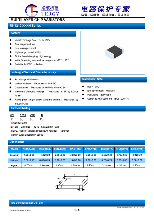
The specimen should be subjected to -40℃, without load for 1000 hours and then Low Temperature Storage stored at room temperature for one two hours. The change of varistor voltage shall be
Pulse Rated peak single pulse transient current : Measured by
8/20µs Pulse
Part Numbering
Mechanical Data
Body ZnO End termination Ag/Ni/Sn Packaging Bulk/Tape Complies with Standard IEC61000-4-5
B0
K0
±0.10 ±0.10
1.88 1.04
T ±0.05 0.22
T2
D0
±0.05 +0.10
0.87 1.50
D1 ±0.05
1.00
P1
P2
±0.10 ±0.05
4.00 2.00
P0 ±0.05
4.00
W ±0.20 8.00
VB
12
10-14
18
15.5-21
21
19-23
24
22-27
27
24-30
30
27-33
33
29-36
37
32-39
39
35-43
47
42-52
53
47-58.5
56
1210贴片自恢复保险丝型号规格书
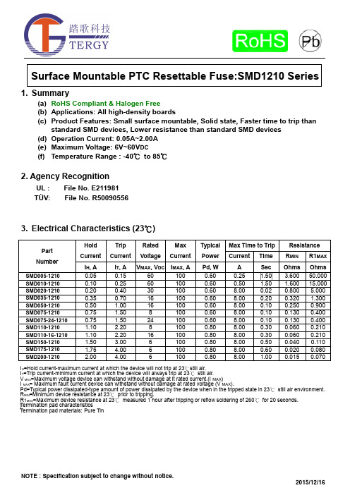
1. Summary(a) RoHS Compliant & Halogen Free(b) Applications: All high-density boards(c) Product Features: Small surface mountable, Solid state, Faster time to trip thanstandard SMD devices, Lower resistance than standard SMD devices (d) Operation Current: 0.05A~2.00A (e) Maximum Voltage: 6V~60V DC(f) Temperature Range : -40℃ to 85℃2. Agency RecognitionUL : File No. E211981TÜV: File No. R500905563.Electrical Characteristics (23℃)I H =Hold current-maximum current at which the device will not trip at 23℃still air. I T =Trip current-minimum current at which the device will always trip at 23℃ still air. V MAX =Maximum voltage device can withstand without damage at it rated current.(I MAX )I MAX = Maximum fault current device can withstand without damage at rated voltage (V MAX ).Pd=Typical power dissipated-type amount of power dissipated by the device when in the tripped state in 23℃ still air environment. R MIN =Minimum device resistance at 23℃ prior to tripping.R 1MAX =Maximum device resistance at 23℃ measured 1 hour after tripping or reflow soldering of 260℃ for 20 seconds. Termination pad characteristics Termination pad materials: Pure Tin4. SMD Product Dimensions (Millimeters)5. Thermal Derating Curve6. Typical Time-To-Trip at 23℃7. Material SpecificationTerminal pad material: Pure TinSoldering characteristics: Meets EIA specification RS 186-9E, ANSI/J-std-002 Category 38. Part Numbering and Marking SystemPart Numbering SystemS M D □□□–□□– 1210Warning: -Operation beyond the specified maximum ratings or improper use may result in damage and possible electrical arcing and/or flame.-PPTC device are intended for occasional overcurrent protection. Application for repeated overcurrentcondition and/or prolonged trip are not anticipated.甲、-Avoid contact of PPTC device with chemical solvent. Prolonged contact will damage the device performance.A = SMD005-1210B = SMD010-1210C = SMD020-1210D = SMD035-1210E = SMD050-1210F = SMD075-1210/ 075-24-1210G = SMD110-1210/ 110-16-1210H = SMD150-1210I = SMD175-1210J = SMD200-1210Current RatingVoltage Rating9. Pad Layouts 、Solder Reflow and Rework RecommendationsThe dimension in the table below provide the recommended pad layout for each SMD 1210 deviceNote 1: All temperatures refer to of the package,measured on the package body surface.Reflow Profile。
DS1210中文资料

DS1210中文资料FEATURES Converts CMOS RAMs into nonvolatile memories Unconditionally write protects when V CC isout of toleranceAutomatically switches to battery when power-fail occursSpace saving 8-pin DIPConsumes less than 100 nA of battery current Tests battery condition on power up Provides for redundant batteries Optional 5% or 10% power-fail detection Low forward voltage drop on the V CC switch Optional 16-pin SOIC surface mount package Optional industrial temperature range of -40°C to +85°CPIN ASSIGNMENTPIN DESCRIPTIONV CCO - RAM Supply V BAT1- + Battery 1TOL - Power Supply Tolerance GND- GroundCE - Chip Enable Input CEO- Chip Enable Output V BAT2- + Battery 2V CCI - + Supply NC- No ConnectDESCRIPTIONThe DS1210 Nonvolatile Controller Chip is a CMOS circuit which solves the application problem of converting CMOS RAM into nonvolatile memory. Incoming power is monitored for an out-of-tolerance condition. When such a condition is detected, chip enable is inhibited to accomplish write protection and the battery is switched on to supply the RAM with uninterrupted power. Special circuitry uses a low-leakage CMOS process whichaffords precise voltage detection at extremely low battery consumption.The 8-pin DIP package keeps PC board real estate requirements to a minimum. By combining the DS1210 Nonvolatile Controller Chip with a CMOS memory and batteries, nonvolatile RAM operation can be achieved.DS1210Nonvolatile Controller ChipVCCOVCCI VBAT2CEO DS1210 8-pin DIP (300-mil)See Mech. Drawings Section NC VCCO NC NC TOL NC GND NC VCCI NC VBAT2NC CEO NC CESee Mech. Drawings SectionDS1210 OPERATIONThe DS1210 nonvolatile controller performs five circuit functions required to battery back up a RAM.First, a switch is provided to direct power from the battery or the incoming supply (V CCI) depending onwhich is greater. This switch has a voltage drop of less than 0.3V. The second function which thenonvolatile controller provides is power-fail detection. The DS1210 constantly monitors the incomingsupply. When the supply goes out of tolerance a precision comparator detects power-fail and inhibits chip enable (CEO). The third function of write protection is accomplished by holding the CEO output signal to within 0.2 volts of the V CCI or batterysupply. If CE input is low at the time power-fail detection occurs, the CEO output is kept in its present state until CE is returned high. The delay of write protection untilthe current memory cycle is completed prevents the corruption of data. Power-fail detection occurs in the range of 4.75 volts to 4.5 volts with the tolerance Pin 3 grounded. If Pin 3 in connected to V CCO, thenpower-fail detection occurs in the range of 4.5 volts to 4.25 volts. During nominal supply conditions CEO will follow CE with a maximum propagation delay of 20ns. The fourth function the DS1210 performs is a battery status warning so that potential data loss is avoided. Each time that the circuit ispowered up the battery voltage is checked with a precision comparator. If the battery voltage is less than2.0 volts, the second memory cycle is inhibited. Battery status can, therefore, be determined byperforming a read cycle after power-up to any location in memory, verifying that memory locationcontent. A subsequent write cycle can then be executed to the same memory location altering the data. Ifthe next read cycle fails to verify the written data, then the batteries are less than 2.0V and data is indanger of being corrupted. The fifth function of the nonvolatile controller provides for batteryredundancy. In many applications, data integrity is paramount. In these applications it is often desirable to use two batteries to ensure reliability. The DS1210 controller provides an internal isolation switch whichallows the connection of two batteries. During battery backup operation the battery with the highestvoltage is selected for use. If one battery should fail, the other will take over the load. The switch to aredundant battery is transparent to circuit operation and to the user. A battery status warning will occurwhen the battery in use falls below 2.0 volts. A grounded V BAT2 pin will not activate a battery-failwarning. In applications where battery redundancy is not required, a single battery should be connected tothe BAT1 pin. The BAT2 battery pin must be grounded. The nonvolatile controller contains circuitry toturn off the battery backup. This is to maintain the battery(s) at its highest capacity until the equipment is powered up and valid data is written to the SRAM. While in the freshness seal mode the CEO and V CCO will be forced to V OL. When the batteries are first attached to one or both of the V BAT pins, V CCO will not provide battery back-up until V CCI exceeds V CCTP, as set by the T OL pin, and then falls below V BAT. Figure 1 shows a typical application incorporating the DS1210 in a microprocessor-based system. Section A shows the connections necessary to write protect the RAM when V CC is less than 4.75 volts and to back up the supply with batteries. Section B shows the use of the DS1210 to halt the processor when V CC is less than 4.75 volts and to delay its restart on power-up to prevent spurious writes.DS1210 SECTION A - BATTERY BACKUP Figure 1BATTERY BACKUP CURRENT DRAIN EXAMPLECONSUMPTIONDS1210 I BAT100 nARAM I CC0210 μATotal Drain10.1 μASECTION B - PROCESSOR RESETABSOLUTE MAXIMUM RATINGS*Voltage on Any Pin Relative to Ground-0.3V to +7.0VOperating Temperature0°C to 70°CStorage Temperature-55°C to +125°CSoldering Temperature260°C for 10 seconds*This is a stress rating only and functional operation of the device at these or any other conditions above those indicated in the operation sections of this specification is not implied. Exposure to absolute maximum rating conditions for extended periods of time may affect reliability. RECOMMENDED DC OPERATING CONDITIONS(0°C to 70°C) PARAMETER SYMBOL MIN TYP MAX UNITS NOTES Pin 3 = GND Supply Voltage V CCI 4.75 5.0 5.5V1Pin 3 = V CCO Supply Voltage V CCI 4.5 5.0 5.5V1 Logic 1 Input V IH 2.2V CC+0.3V1 Logic 0 Input V IL-0.3+0.8V12.0 4.0V1, 2 Battery Input V BAT1,V BAT2(0°C to 70°C; V CCI = 4.75 to 5.5V PIN 3 = GND)CAPACITANCE(T A = 25°C) PARAMETER SYMBOL MIN TYP MAX UNITS NOTES Input Capacitance C IN5pFOutput Capacitance C OUT7pF(0°C to 70°C; V CCI = 4.75V to 5.5V, PIN 3 = GND)NOTES:1.All voltages are referenced to ground.2.Only one battery input is required. Unused battery inputs must be grounded.3.Measured with V CCO and CEO open.4.I CC01is the maximum average load which the DS1210 can supply to the memories.5.Measured with a load as shown in Figure 2.6.I CC02is the maximum average load current which the DS1210 can supply to the memories in thebattery backup mode.7.t CE max. must be met to ensure data integrity on power loss.8.CEO can only sustain leakage current in the battery backup mode.TIMING DIAGRAM: POWER-UPTIMING DIAGRAM: POWER-DOWNOUTPUT LOAD Figure 2。
Littelfuse力特1210自恢复保险丝规格书

© 2015 Littelfuse, Inc.Specifications are subject to change without notice. Revised: 04/08/15The 1210L Series PTC provides surface mount overcurrent protection for applications where space is at a premium and resettable protection is desired.Electrical CharacteristicsI hold = Hold current: maximum current device will pass without tripping in 20°C still air. I trip = Trip current: minimum current at which the device will trip in 20°C still air.V max = Maximum voltage device can withstand without damage at rated current (I max) I max = Maximum fault current device can withstand without damage at rated voltage (V max )P d = Power dissipated from device when in the tripped state at 20°C still air.R min = Minimum resistance of device in initial (un-soldered) state.R typ = Typical resistance of device in initial (un-soldered) state.R 1max =M aximum resistance of device at 20°C measured one hour after tripping or reflow soldering of 260°C for 20 sec.DescriptionApplications• U SB peripherals • D isk drives • C D-ROMs • P C motherboards - plug and play protection• M obile phones - battery and port protection • P DAs / digital cameras • G ame console port protectionFeatures• R oHS compliant, lead-free and halogen-free • F ast response to fault currents • C ompact design saves board space• L ow resistance • L ow-profile • C ompatible with high temperature soldersAgency ApprovalsCaution: Operation beyond the specified rating may result in damage and possible arcing and flame.© 2015 Littelfuse, Inc.Specifications are subject to change without notice.Revised: 04/08/15T emperature Rerating Curve-40-30-20-1010203040506070808510%30%50%70%90%110%130%150%170%Temperature (°C)P e r c e n t a g e o f R a t e dC u r r e n tAverage Time Current CurvesThe average time current curves and Temperature Rerating curve performance is affected by a number or variables, and these curves provided as guidance only. Customer must verify the performance in their application.0.10A 0.14A 0.20A 0.50A 0.75A /33V 0.75A /24V 0.75A 1.10A /16V 1.10A /33V 1.10A 1.25A 1.25A /6V 1.50A /12V 1.50A 1.50A /24V 1.60A /12V 1.60A 1.60A /8V 2.00A 2.60A100010000s1210L OLD0.05A 0.10A 0.20A 0.35A 0.50A 0.75A 1.10A 1.50A 1.75A 2.00A0.010.101.0010.00100.000.101.0010.00T i m e i n S e c o n d sCurrent in Amperes1210L0.05A 0.10A 0.20A 0.35A 0.50A 0.75A 0.75A /241.10A 1.50A 1.75A 2.00AThe temperature rerating data is only for reference, please contact Littelfuse technical support for detail temperature rerating information.Note:Typical Temperature rerating curve, refer to table for derating data© 2015 Littelfuse, Inc.Specifications are subject to change without notice. Revised: 04/08/15Environmental SpecificationsPhysical Specifications-- All temperature refer to topside of the package, measured on the package body surface -- If reflow temperature exceeds the recommended profile, devices may not meet the performance requirements-- Recommended reflow methods: IR, vapor phase oven, hot air oven, N 2 environment for lead-- Recommended maximum paste thickness is 0.25mm (0.010 i nch)-- Devices can be cleaned using standard industry methods and solvents -- Devices can be reworked using the standard industry practices© 2015 Littelfuse, Inc.Specifications are subject to change without notice.Revised: 04/08/15(.040)MARKING CODE VARIES WITH AMPERAGE RATING(See Electrical Characteristics Table)SHOWN IS 1.5AMP RATING© 2015 Littelfuse, Inc.Specifications are subject to change without notice. Revised: 04/08/15=10,000 Y =4,000 W =3,000 P =2,000Tape & Reel-A: Automotive grade Blank: Standard version© 2015 Littelfuse, Inc.Specifications are subject to change without notice.Revised: 04/08/15WARNING• Users shall independently assess the suitability of these devices for each of their applications• Operation of these devices beyond the stated maximum ratings could result in damage to the devices and lead to electrical arcing and/or fire• These devices are intended to protect against the effects of temporary over-current or over-temperature conditions and are not intended to perform as protective devices where such conditions are expected to be repetitive or prolonged in duration• Exposure to silicon-based oils, solvents, electrolytes, acids, and similar materials can adversely affect the performance of these PPTC devices• These devices undergo thermal expansion under fault conditions, and thus shall be provided with adequate space and be protected against mechanical stresses • Circuits with inductance may generate a voltage (L di/dt) above the rated voltage of the PPTC device.。
msc1210中文
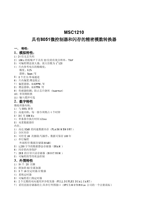
参数
模拟输入 AIN0-AIN7 AINCOM 模拟输入范
围
全输入电压范围 差分输入阻抗
输入电流 带宽
快速沉积滤波器 Sinc2滤波器 Sinc2滤波器
可编程增益放大器 输入电容 输入漏电流 熔断电流
偏移DAC 偏移DAC范围 偏移DAC单调性 偏移DAC增益偏差 偏移DAC增益偏差漂移
条件
缓冲区关闭 缓冲区打开 IN+ - IN- 看图4 缓冲区关闭 缓冲区打开
256
内部 MOVX 静态随机存储器 字节 1024
1024
1024
1024
数
外部可存取存储器 字节数
程序 64K 数据 64K
程序 64K 数据 64K
程序 64K 数据 64K
程序 64K 数据 64K
注释 1 所有器件的外围特性相同 仅闪存容量不同 2 类型号的最后一位数字代表片内闪存容量 的大小= 2N KB
DC下 fCM = 60Hz, fDATA = 10Hz fCM = 50Hz, fDATA = 50Hz fCM = 60Hz, fDATA = 60Hz fSIG = 50Hz, fDATA = 50Hz fSIG = 60Hz, fDATA = 60Hz
DC下 dB =–20log( VOUT/ VDD)
MSC1210YX
最小值
典型值
最大值
单位
AGND-0.1 AGND
1
5/PGA 0.5
AVDD+0.1
AVDD-1.5
+VREF/PGA
0.469 • fDATA 0.318 • fDATA 0.262 • fDATA
9 0.5 +6
128
横河AQ1210系列光时域反射仪说明书

现场多用测试仪OTDRAQ1210系列安全可靠操作方便快速启动10030紧凑机身、长效电池外形大小如A5纸张,重量大约1Kg (2.2Lbs)。
使用电池可工作10小时。
触摸屏与按键相结合的直观操作AQ1210配备了5.7英寸多点触控的电容式触摸屏,还有一个适合 现场操作的旋钮按键。
连接能力通过Wi-Fi 或以太网进行数据传输和远程控制。
增强的OTDR 性能测量多达128分路的PON 系统。
高速实时测量。
提高工作效率的功能和特点多光纤测量、智能链路分析功能、PDF 报告。
一机多能用于多种任务的各种可选功能。
OTDRFSTVLSOPCOL TS列全尺寸 210mm (W)×148mm (H)结构紧凑、功能完备智能、紧凑、多功能OTDRAQ1210系列4产品型号共有7款机型可供选择,满足用户安装和维护各种光网络的需求(LAN/PON/FTTA/FTTH/FTTB)。
产品型号&选型指南产品型号&选型指南AQ1210系列5触摸屏与按键相结合的直观操作双操作模式AQ1210配备了5.7英寸多点触控触摸屏,可方便的进行触控操作和曲线缩放。
此外它还带有一个适合现场操作的旋钮按键。
触摸屏与按键相结合的直观操作直接保存数据只需按“直接保存”图标,就可以根据用户先前的选择以SOR 、PDF 或全部两种格式来保存测量数据。
长电池续航超过10小时的续航能力!用户不必担心日常工作中电池电量耗尽的问题。
AQ1210锂电池拥有的强劲电力,可使它在Telcordia 标准条件下持续供电10个小时。
快速启动小于10秒钟!从完全关机状态到测量准备完成仅需不到10秒的时间!放大曲线窗口只需点击专用图标即可放大曲线显示窗口,便于查看和操作。
曲线区域放大后的大小约为标准大小的两倍。
测量条件设置窗口可以在OTDR 初始屏幕中切换测量条件,用于进行多条件测量。
AQ1210系列61 × 81 × 641 × 1281 × 16增强的OTDR 性能PON 优化利用出色的硬件性能和先进的分析算法,AQ1210可以通过多端口分路器(高达1×128)*准确地描述无源光网络(PON)。
1210使用说明书
HYP1210微机电容器保护装置使用说明书USERGUIDE®ZHEJIANG HUAYI ELECTRIC POWER AUTOMATION CO.,LTD ®ZHEJIANG HUAYI ELECTRIC POWER AUTOMA TION CO.,LTD目录1.适用范围 (4)2.装置功能及保护原理简述 (4)2.1 电气参数测量 (4)2.2 延时速断保护 (4)2.3 定时限过流保护 (4)2.4中性点不平衡电流保护(适用于电容器组双Y形接线) (4)2.5零序电压保护(开口三角电压,适用于单组电容器) (4)2.6过电压保护 (4)2.7低电压保护 (4)2.8 PT断线报警 (5)2.9定值错误报警 (5)2.10装置故障报警 (5)3、技术参数 (5)4.按键功能及操作方法 (6)4.1按键功能 (6)4.1.1“▼”搜索键与功能键 (6)4.1.2“◄►”显示、进入修改状态及移动、修改键 (6)4.1.3“▲”修改、操作键 (6)4.1.4“■信号复归”键 (6)4.2输入密码的方法: (6)4.3搜索方法(适用于定点显示和进入定值区的显示): (6)4.4密码种类 (6)5.数码管的显示种类 (6)5.1 数码管显示说明 (6)5.2几种显示列表 (6)5.2.1循环显示(供运行人员使用) (7)5.2.2定点显示 (7)5.2.3定值区的显示(输入密码1111) (7)5.2.4有报警或预告时的显示: (8)6.调试大纲(适用于调试人员及维护人员) (9)6.1查看、输入或修改保护定值: (9)6.2开关量的检查 (9)6.3保护继电器的出口检查 (9)6.4模拟量输入检查及精度检查 (9)6.4.1电流校准 (9)6.4.2电压校准 (9)6.4.3不平衡电流校准 (9)6.6保护试验 (10)6.6.1延时速断与定时限过流保护测试 (10)6.6.2过电压保护测试 (10)6.6.3低电压保护测试 (10)®ZHEJIANG HUAYI ELECTRIC POWER AUTOMA TION CO.,LTD®ZHEJIANG HUAYI ELECTRIC POWER AUTOMA TION CO.,LTD 36.6.4不平衡电流保护测试 (10)6.6.5零序电压保护测试 (10)6.6.6保护动作时间测试 (10)6.6.7 PT回路断线报警 (10)7.机箱结构及端子图 (11)7.1装置组成 (11)7.1机箱结构图与说明 (11)7.2安装与开孔图 (12)7.3装置端子图 (12)8.运行人员注意事项及要求 (13)9.检修及维护 (14)附录1:HYP1210微机电容器保护装置原理图 (1)附录2:HYP1210微机电容器保护装置原理接线图 (2)1.适用范围HYP1210微机电容器保护装置适用于6-66KV 中性点不接地系统,作为电容器的成套保护和监视报警装置,适用于高低压开关柜、箱式变电站等使用电容补偿的场合。
FPGA可编程逻辑器件芯片EP1C12Q240I7N中文规格书

Description of OperationADSP-BF54x Blackfin Processor Hardware ReferenceA processor reset disables the SPORTs by clearing the SPORTx_TCR1, SPORTx_TCR2, SPORTx_RCR1, and SPORTx_RCR2 registers (including the TSPEN and RSPEN enable bits) and the SPORTx_TCLKDIV , SPORTx_RCLKDIV , SPORTx_TFSDIVx , and SPORTx_RFSDIVx clock and frame sync divisor regis-ters. Any ongoing operations are aborted.Clearing the TSPEN and RSPEN bits disables the SPORTs and aborts any ongoing operations. Status bits are also cleared. Configuration bits remain unaffected and can be read by the software in order to be altered or over-written. To disable the SPORT output clock, disable the SPORT. Note that disabling a SPORT through TSPEN /RSPEN may shortenany currently active pulses on the TFSx /RFSx and TSCLKx /RSCLKx outputs, if these signals are configured to be generated internally.When disabling the SPORT from multichannel operation, first disable TSPEN and then disable RSPEN . Note both TSPEN and RSPEN must be dis-abled before re-enabling. Disabling only TX or RX is not allowed.Setting SPORT ModesSPORT configuration is accomplished by setting bit and field values in configuration registers. Each SPORT must be configured prior to being enabled. Once the SPORT is enabled, further writes to the SPORT con-figuration registers are disabled (except for SPORTx_RCLKDIV ,SPORTx_TCLKDIV , and multichannel mode channel select registers). To change values in all other SPORT configuration registers, disable the SPORT by clearing TSPEN in SPORTx_TCR1 and/or RSPEN in SPORTx_RCR1.Each SPORT has its own set of control registers and data buffers. These registers are described in detail in the “SPORT Registers” section. All control and status bits in the SPORT registers are active high unless other-wise noted.Description of OperationADSP-BF54x Blackfin Processor Hardware Reference Table 24-3 shows the dependencies of bits in the SPORT configuration register when the SPORT is in multichannel mode.Frame Syncs in Multichannel ModeAll receiving and transmitting devices in a multichannel system must have the same timing reference. The RFSx signal is used for this reference, indi-cating the start of a block or frame of multichannel data words.Table 24-3. Multichannel Mode Configuration SPORTx_RCR1 orSPORTx_RCR2SPORTx_TCR1 or SPORTx_TCR2Notes RSPENTSPEN Set or clear both IRCLK-Independent -ITCLK Independent RDTYPETDTYPE Independent RLSBITTLSBIT Independent IRFS-Independent -ITFS Ignored RFSRTFSR Ignored -DITFS Ignored LRFSLTFS Independent LARFSLATFS Both must be 0RCKFETCKFE Set or clear both to same value SLENSLEN Set or clear both to same value RXSETXSE Independent RSFSETSFSE Both must be 0RRFST TRFST Ignored。
1210的钽电容
1210的钽电容摘要:1.钽电容的概述2.钽电容的特点3.1210 钽电容的规格参数4.1210 钽电容的应用领域5.钽电容的选购与使用注意事项正文:一、钽电容的概述钽电容,又称钽电解电容,是一种以钽为阳极材料的电解电容器。
钽电容具有体积小、容量大、稳定性高、寿命长等特点,广泛应用于各类电子设备中。
二、钽电容的特点1.体积小:钽电容的体积较其他电容器更小,可以节省电路板空间。
2.容量大:钽电容具有较高的电容量,能够满足多种应用场景的需求。
3.稳定性高:钽电容的工作电压稳定,温度特性好,适合在恶劣环境下使用。
4.寿命长:钽电容的使用寿命较长,可以在长时间内保持稳定的工作性能。
5.良好的抗干扰性能:钽电容具有较强的抗电磁干扰和抗射频干扰能力。
三、1210 钽电容的规格参数1210 钽电容是指尺寸为12mm×10mm 的钽电容器。
其主要规格参数包括:1.电容值:钽电容的电容值有多种选择,如10pF、100pF、1nF 等。
2.额定电压:钽电容的额定电压有3V、5V、10V、16V 等不同规格。
3.工作温度:钽电容的工作温度范围为-55℃至+105℃。
4.存储温度:钽电容的存储温度范围为-55℃至+125℃。
四、1210 钽电容的应用领域1210 钽电容广泛应用于各类电子设备和电路中,如:1.通信设备:手机、无线电、卫星通信系统等。
2.计算机硬件:内存条、主板、显卡等。
3.消费电子产品:电视、音响、照相机等。
4.医疗设备:心电图仪、超声波设备等。
5.工业控制:自动化控制系统、传感器等。
五、钽电容的选购与使用注意事项1.选购时,应根据电路需求选择合适的电容值、额定电压和工作温度等参数。
2.钽电容在焊接时,应注意焊接温度不要过高,以免损坏电容器。
3.在使用过程中,应注意保持钽电容的工作电压和温度在规定范围内,避免长时间过载使用。
msc1210芯片资料(中文)

具有 8051 微处理器及闪存的精密模数转换器
一 特性 1 模拟特性 1 24 位无丢失码 2 10Hz 的低噪声下具 22 位有效分辨率 75nV 3 可编程增益放大器 PGA 放大倍数为 1 128 4 片内参考电压的精确度 精度 0.2 漂移 5ppm/ 5 8 个差分/单端通道 6 片内偏置/增益校正 7 偏置漂移 0.02 ppm/ 8 增益漂移 0.5 ppm/ 9 传感器检测 防止芯片烧坏 burn out 10 单周期转换 11 输入缓冲可选 2 数字特性 微处理器内核 1 与 8051 兼容 2 高速内核 每一指令周期占 4 个时钟 3 DC 至 33MHz 4 单条指令执行时间 121ns 5 双重数据指针 内存 1 高达 32KB 的闪速数据内存 FLASH MEMORY 2 分区闪存 3 可经受 1M 次擦除/写操作 数据可保存 100 年 4 系统内部连续编程 串行编程 外部程序/数据存储器 64KB 5 1,280 字节的数据静态存储器 SRAM 6 闪存的内容保护 7 2KB 的引导只读存储器 BOOT ROM 8 可编程的等待状态控制 3 外围特性 1 34 个 I/O 脚 2 附加的 32 位累加器 3 3 个 16 位定时器/计数器 4 系统定时器 5 可编程看门狗定时器 6 2 个完整的双向通用异步收发器 FULL DUPLEX DUAL UART 7 采用直接存储器的主/从串行外围接口 SPI 为 MOTOROLA 公司的一个注册商标 8 16 位 PWM 9 电源管理控制 10 空闲模式下电流<1mA 11 停止模式下电流<1uA
注释
1
若需查询更多电流规格与封装资料
请登陆网站
四 最大额定值 绝对值 1 1 模拟输入 输入电流 输入电流 输入电压 2 供电电源 DVDD 相对于 DGND AVDD 相对于 AGND AGND 相对于 DGND VREF 相对于 AGND
1210标准封装尺寸

1210标准封装尺寸
1210标准封装是一种电子元器件封装类型,通常用于表面贴装技术(SMT)应用。
它是一种小型尺寸封装,尺寸为12mm x 10mm。
具体来说,1210标准封装的尺寸为12mm(长度) x 10mm (宽度),因此也被称为3216封装,代表其尺寸为32 x 16百分之一英寸。
1210标准封装适用于一些小型电子元件,如电容、电感、保险丝、电阻器等。
其小尺寸使得它能够在紧凑的电路板上实现高密度的布局。
需要注意的是,尽管1210封装是标准尺寸,但在不同的应用和行业中,可能会有一些微小的尺寸变化。
因此,在选择和使用具体元件时,最好参考相关的产品规格表或厂商提供的数据来确定封装的精确尺寸。
MD1210资料

Initial Release High Speed, Dual MOSFET DriverFeatures6.0ns rise and fall time with 1000pF load 2.0A peak output source/sink current1.2V to 5V input CMOS compatible4.5V to 13V total supply voltageSmart Logic thresholdLow jitter designDual matched channelsOutputs can swing below groundLow inductance packageThermally-enhanced packageApplicationsMedical ultrasound imagingPiezoelectric transducer driversNondestructive evaluationPIN diode driverClock driver/bufferHigh speed level translator General DescriptionThe Supertex MD1210 is a high speed, dual MOSFET driver. It is designed to drive high voltage N- and P-channel MOSFET transistors for medical ultrasound applications and other application requiring a high output current for a capacitive load. The high-speed input stage of the MD1210 can operate from 1.2 to 5.0 volt logic interface with an optimum operating input signal range of 1.8 to 3.3 volts. An adaptive threshold circuit is used to set the level translator switch threshold to the average of the input logic 0 and logic 1 levels. The input logic levels may be ground referenced, even though the driver is putting out bipolar signals. The level translator uses a proprietary circuit, which provides DC coupling together with high-speed operation.The output stage of the MD1210 has separate power connections enabling the output signal L and H levels to be chosen independently from the supply voltages used for the majority of the circuit. As an example, the input logic levels may be 0 and 1.8 volts, the control logic may be powered by +5.0 and –5.0 volts, and the output L and H levels may be varied anywhere over the range of –5.0 to +5.0 volts. The output stage is capable of peak currents of up to ±2.0 amps, depending on the supply voltages used and load capacitance present.The OE pin serves a dual purpose. First, its logic H level is used to compute the threshold voltage level for the channel input level translators. Secondly, when OE is low, the outputs are disabled, with the A output high and the B output low. This assists in properly pre-charging the AC coupling capacitors that may be used in series in the gate drive circuit of an external PMOS and NMOS transistor pair.Typical Application CircuitNR013105Ordering InformationPackage Option Product Marking InformationDevice12-lead 4x4x0.9 QFN1stline 1210 Device Number MD1210 MD1210K62ndline YWLL Year, Week Code, Lot Number Example: 5A88 means Lot #88 of first or second week in 2005Absolute Maximum Ratings*Pin1→DC Electrical Characteristics(Over operating conditions unless otherwise specified, V H =V DD 1=V DD 2=12V, V L =V SS 1=V SS 2=0V, V OE =3.3V, T J = 25°C)Sym Parameter Min Typ Max Units ConditionsV DD -V SS Logic supply voltage 4.5 13 V V SS Low side supply voltage -5.5 0VV H Output high supply voltage V SS +2.0 V DD VV L Output low supply voltage V SS V DD -2 V I DD1Q V DD1 quiescent current 0.55 mA I DD2Q V DD2 quiescent current 10 µA I HQ V H quiescent current 10 µA No input transitionsI DD1 V DD1 average current 0.88 mA I DD2 V DD2 average current 6.6 mA I H V H average current 23 mA One channel on at 5.0Mhz, No load V IH Input logic voltage high V OE -0.3 5.0 VV IL Input logic voltage low 0 0.3 V I IH Input logic current high 1.0 µA I IL Input logic current low 1.0 µA For logic inputs INA and INB.V IH OE Input logic voltage high 1.2 5.0 V V IL OE Input logic voltage low 00.3VR IN Input logic impedance to GND12 20 30 K Ω For logic input OEC IN Logic input capacitance 5.0 10 pFAll InputsθJA Thermal resistance to air 47 °C/W1oz. 4-layer 3x4inch PCB with thermalpad and thermal via array.θJCThermal resistance to case7.0°C/WOutputs (V H=VDD1=V DD 2=12V, V L =V SS 1=V SS 2=0V, V OE =3.3V, T J =25°C)Sym Parameter Min Typ Max UnitsConditionsR SINK Output sink resistance12.5 Ω I SINK =50mA R SOURCE Output source resistance 12.5 Ω I SOURCE =50mA I SINK Peak output sink current 2.0 A I SOURCEPeak output source current2.0AV DD -V SS , Logic Supply Voltage -0.5V to +13.5V V H , Output High Supply Voltage V L -0.5V to V DD +0.5V V L , Output Low Supply Voltage V SS -0.5V to V H +0.5VV SS , Low Side Supply Voltage -7.0V to +0.5VLogic Input LevelsV SS -0.5V to V SS +7.0VMaximum Junction Temperature +125°CStorage Temperature-65°C to 150°C*Absolute Maximum Ratings are those values beyond which damage to the device may occur. Functional operation under these conditions is not implied. Continuous operation of the device at the absolute rating level may affect device reliability. All voltages are referenced to device ground.Top ViewAC Electrical Characteristics (V H=VDD1=V DD 2=12V, V L =V SS 1=V SS 2=0V, V OE =3.3V, T J =25°C)Sym Parameter Min Typ Max Units Conditions t irf Inputs or OE rise & fall time10nsLogic input edge speed requirementt PLH Propagation delay when output is from low to high 7.0 nst PHL Propagation delay when output is from high to low 7.0 nst POE Propagation delay OE to outputs9.0 ns No load, see timing diagram Input signal rise/fall time 2ns t r Output rise time 6.0 ns t f Output fall time6.0 ns l t r - t f l Rise and fall time matching1.0TBDnsC LOAD =1000pF, see timing diagram Input signal rise/fall time 2nsl t PLH -t PHL l Propagation low to high and high to low matching 1.0 ns∆t dmPropagation delay Match±2.0TBDnsDevice to device delay matchLogic Truth TableLogic InputsOutputOE INA INB OUTA OUTB H L LV HV HH L H V H V LH H L V L V H H H H V L V L L X X V H V LIN OUT r f3.3V0V0VTiming DiagramSimplified Block DiagramPropagation DelayLogic Input ThresholdMD1210 DetailedBlockDiagramApplication InformationFor proper operation of the MD1210, low inductance bypass capacitors should be used on the various supply pins. The GND input pin should be connected to the digital ground. The INA, INB, and OE pins should be connected to their logic source with a swing of GND to logic level high which is 1.2 to 5.0 volts. Good trace practices should be followed corresponding to the desired operating speed. The internal circuitry of the MD1210 is capable of operating up to 100MHz, with the primary speed limitation being the loading effects of the load capacitance. Because of this speed and the high transient currents that result with capacitive loads, the bypass capacitors should be as close to the chip pins as possible. Unless the load specifically requires bipolar drive, the V SS1, V SS2, and V L pins should have low inductance feed-through connections directly to a ground plane. If these voltages are not zero, then they need bypass capacitors in a manner similar to the positive power supplies. The power connections V DD1 and V DD2 should have a ceramic bypass capacitor to the ground plane with short leads and decoupling components to prevent resonance in the power leads. A common capacitor and voltage source may be used for these two pins, which should always have the same DC voltage applied. For applications sensitive to jitter and noise, separate decoupling networks may be used for V DD1 and V DD2. The supplied voltages of V H and V L determine the output logic levels. These two pins can draw fast transient currents of up to 2.0A, so they should be provided with an appropriate bypass capacitor located next to the chip pins. A ceramic capacitor of up to 1.0µF may be appropriate, with a series ferrite bead to prevent resonance in the power supply lead coming to the capacitor. Pay particular attention to minimizing trace lengths and using sufficient trace width to reduce inductance. Surface mount components are highly recommended. Since the output impedance of this driver is very low, in some cases it may be desirable to add a small series resistor in series with the output signal to obtain better waveform integrity at the load terminals. This will of course reduce the output voltage slew rate at the terminals of a capacitive load.Pay particular attention to the parasitic coupling from the driver output to the input signal terminals. This feedback may cause oscillations or spurious waveform shapes on the edges of signal transitions. Since the input operates with signals down to 1.2V even small coupled voltages may cause problems. Use of a solid ground plane and good power and signal layout practices will prevent this problem. Be careful that the circulating ground return current from a capacitive load cannot react with common inductance to cause noise voltages in the input logic circuitry.MD1210Pin DescriptionV DD 1 High side analog circuit and level shifter supply voltage. Should be at the same potential as V DD 2. V DD 2 High side gate drive supply voltageV SS 1 Low side analog circuit and level shifter supply voltage. Should be at the same potential as V SS 2. V SS 2 Low side gate drive supply voltage V H Supply voltage for P-channel output stage V L Supply voltage for N-channel output stage GND Logic input ground referenceOE Output-enable logic input. When OE is high, (V OE +V GND )/2 sets the threshold transition between logic level high and low for INA and INB. When OE is low, OUTA is at V H and OUTB is at V L regardless of INA and INB. INA Logic input. Controls OUTA when OE is high. Input logic high will cause the output to swing to V L . Input logic low will cause the output to swing to V H .INBLogic input. Controls OUTB when OE is high. Input logic high will cause the output to swing to V L . Input logic low will cause the output to swing to V H .OUTAOutput driver. Swings from V H to V L . Intended to drive the gate of an external P-channel MOSFET via a series capacitor. When OE is low, the output is disabled. OUTA will swing to V H turning off the external P-channel MOSFET.OUTBOutput driver. Swings from V H to V L. Intended to drive the gate of an external N-channel MOSFET via a series capacitor. When OE is low, the output is disabled. OUTB will swing to V L turning off the external N-channel MOSFET.Pin ConfigurationPin #Function1 INA2 V L3 INB4 GND5 V SS 16 V SS 27 OUTB 8 V H9 OUTA 10 V DD 2 11 V DD 112 OE NoteThermal Pad, and substrate areconnected to Pin#5,V SS 1Doc.#: DSFP-MD1210 NR013105。
MAT02中文资料
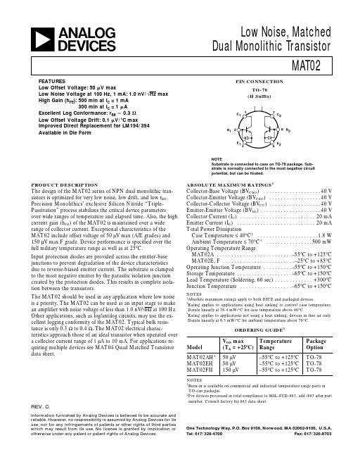
One Technology Way, P.O. Box 9106, Norwood, MA 02062-9106, U.S.A. Tel: 617/329-4700 Fax: 617/326-8703
元器件交易网MAT02来自SPECIFICATIONSELECTRICAL CHARACTERISTICS (@ V
PRODUCT DESCRIPTION
ABSOLUTE MAXIMUM RATINGS 1
The design of the MAT02 series of NPN dual monolithic transistors is optimized for very low noise, low drift, and low rBE. Precision Monolithics’ exclusive Silicon Nitride “TriplePassivation” process stabilizes the critical device parameters over wide ranges of temperature and elapsed time. Also, the high current gain (hFE) of the MAT02 is maintained over a wide range of collector current. Exceptional characteristics of the MAT02 include offset voltage of 50 µV max (A/E grades) and 150 µV max F grade. Device performance is specified over the full military temperature range as well as at 25°C. Input protection diodes are provided across the emitter-base junctions to prevent degradation of the device characteristics due to reverse-biased emitter current. The substrate is clamped to the most negative emitter by the parasitic isolation junction created by the protection diodes. This results in complete isolation between the transistors. The MAT02 should be used in any application where low noise is a priority. The MAT02 can be used as an input stage to make an amplifier with noise voltage of less than 1.0 nV/√Hz at 100 Hz. Other applications, such as log/antilog circuits, may use the excellent logging conformity of the MAT02. Typical bulk resistance is only 0.3 Ω to 0.4 Ω. The MAT02 electrical characteristics approach those of an ideal transistor when operated over a collector current range of 1 µA to 10 mA. For applications requiring multiple devices see MAT04 Quad Matched Transistor data sheet.
Agilent 1200 Infinity 系列产品介绍说明书

• Pump: New next generation inlet valves for better performance • Detectors: Next generation 1290 Infinity DAD technology • HiP Autosampler: leveraging of many parts of the 1290 Infinity
• 30 % Price Reduction by March 1st, attractive upfront contracts • Based on
– proven robustness – 2x higher than 1100 Series at introduction – Increased parts lifetime / longer maintenance intervalls – new design-for-supportability technology for faster maintenance,
1260 Infinity Quat./Iso LC 1220 Infinity LC
6
8
10 flow
Page 6
1260 Quaternary LC and 1220 Gradient LC
RRLC Performance for EVERY LAB!
10x productivity increase and improved data quality!
Conventional 4.6x150, 5µm Resolution peak 5 = 4.20 Run time 11 min
自恢复保险丝SMD1210封装参数型号规格书大全
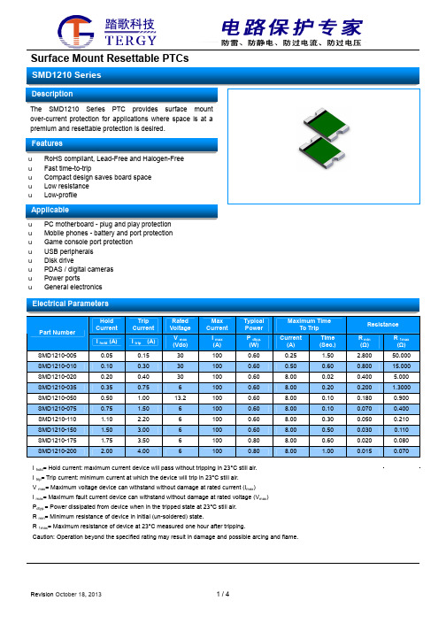
The SMD1210 Series PTC providessurfacemount over-current protection for applications where space is at a premium and resettable protection is desired.u RoHS compliant, Lead-Free and Halogen-Free u Fast time-to-tripu Compact design saves board space u Low resistance uLow-profileu Mobile phones - battery and port protection u Game console port protection u USB peripherals u Disk driveu PDAS / digital cameras u Power portsuGeneral electronicsHold Current Trip Current Rated Voltage Max Current Typical Power Maximum TimeTo Trip Resistance Part NumberI hold (A)I trip (A) V max (Vdc) I max (A) P dtyp. (W) Current (A) Time (Sec.) R min (Ω) R 1max (Ω) SMD1210-005 0.05 0.15 30 100 0.60 0.25 1.50 2.800 50.000 SMD1210-010 0.10 0.30 30 100 0.60 0.50 0.60 0.800 15.000 SMD1210-020 0.20 0.40 30 100 0.60 8.00 0.02 0.400 5.000 SMD1210-035 0.35 0.75 6 100 0.60 8.00 0.20 0.200 1.3000 SMD1210-050 0.50 1.00 13.2 100 0.60 8.00 0.10 0.180 0.900 SMD1210-075 0.75 1.50 6 100 0.60 8.00 0.10 0.070 0.400 SMD1210-110 1.10 2.20 6 100 0.60 8.00 0.30 0.050 0.210 SMD1210-150 1.50 3.00 6 100 0.60 8.00 0.50 0.030 0.110 SMD1210-175 1.75 3.50 6 100 0.80 8.00 0.60 0.020 0.080 SMD1210-2002.004.0061000.808.001.000.0150.070I hold = Hold current: maximum current device will pass without tripping in 23°C still air. I trip = Trip current: minimum current at which the device will trip in 23°C still air. V max = Maximum voltage device can withstand without damage at rated current (I max ) I max = Maximum fault current device can withstand without damage at rated voltage (V max ) P dtyp.= Power dissipated from device when in the tripped state at 23°C still air. R min = Minimum resistance of device in initial (un-soldered) state.R 1max = Maximum resistance of device at 23°C measured one hour after tripping.Caution: Operation beyond the speci fied rating may result in damage and possible arcing and flame.Profile FeaturePb-Free Assembly Average Ramp-Up Rate (T S max to T P ) 3°C/second max. Preheat :Temperature Min (T S min) Temperature Max (T S max) Time (T S min to T S max) 150°C 200°C60-180 seconds Time maintained above:Temperature(TL) Time (tL)217°C60-150 seconds Peak/Classification Temperature(T P ): 260°C Time within 5°C of actual peak: Temperature20-40 seconds Ramp-down Rate:6°C/ second max. Time 25°C to Peak Temperature8 minutes max.Note: All temperatures refer to of the package, measured on the package body surface.Solder reflowDue to “Lead Free ” nature, Temperature and Dwelling time for the soldering zone is higher than those for Regular. This may cause damage to other components.1.Recommended max past thickness > 0.25mm.2.Devices can be cleaned using standard methods and aqueous solvent.3.Rework use standard industry practices.4.Storage Environment : < 30/ 60%RH℃Caution:1.If reflow temperatures exceed the recommended profile, devices may not meet the performance requirements.2.Devices are not designed to be wave soldered to the bottom side of the board.Terminal pad material Pure TinSoldering CharacteristicsMeets EIA specification RS 186-9E, ANSI/J-std-002 Category 3holdA B C DeviceNominalNominal Nominal 1210 Series2.001.002.80Model -40℃-20℃0℃25℃ 40℃50℃60℃ 70℃ 85℃SMD1210-005 0.08 0.07 0.06 0.05 0.04 0.04 0.03 0.03 0.02 SMD1210-010 0.16 0.14 0.12 0.10 0.08 0.07 0.06 0.05 0.03 SMD1210-020 0.29 0.26 0.22 0.20 0.16 0.14 0.13 0.11 0.08 SMD1210-035 0.47 0.45 0.40 0.35 0.33 0.28 0.24 0.21 0.18 SMD1210-050 0.76 0.67 0.58 0.50 0.43 0.40 0.36 0.32 0.28 SMD1210-075 1.00 0.97 0.86 0.75 0.64 0.59 0.54 0.48 0.40 SMD1210-110 1.69 1.48 1.29 1.10 0.88 0.76 0.65 0.57 0.43 SMD1210-150 2.13 1.92 1.71 1.50 1.26 1.14 1.01 0.89 0.71 SMD1210-175 2.54 2.30 2.02 1.75 1.47 1.33 1.18 1.05 0.86 SMD1210-2002.902.632.312.001.681.521.351.200.98Maximum ambient operating temperature (Tmao) vs .hold current(I hold)u Operation beyond the specified maximum ratings or improper use may result in damage and possible electrical arcing and/or flame.u PPTC device are intended for occasional over-current protection. Application for repeated over-current condition and/or prolonged trip are not anticipated.uAvoid contact of PPTC device with chemical solvent. Prolonged contact will damage the device performance.0.33 (8.4)0.512(13.0)Arbor Hole DiameterDimensions are in inches (and millimeters)0.157 (4.0) 0.059 (1.5)Diameter Cover tape(4.0)(5.4)。
1210贴片取样电阻

P max.
Power ratio(%)
Ambient
Temp. ( C )
Figure 1
5.2 Rated Voltage:
The rated voltage is calculated by the following formula: E = P*R E=Rated Voltage(V) P=Rated Power(W) R=Resistance Value(Ω)
R020
RL13FT
F
Manufacture Label
9.2 Customer Label ( By customer request ): Lead-Free Products
TA-I TECH
Product Spec. Customer No:
1210 1%(T) 0.02Ω 105A702723 RL13FTNR020
Low Resistance for 1210 Halogen-Free
4. Dimensions:
TRL-130S032D
2012/11/26 2 /8
R020
UNIT: mm
Type RL13
L 3.10 ±0.20
W 2.55 ± 0.2
C 0.50 ±0.30
d 0.50 ± 0.20
t 0.55 ± 0.15
Refer to paragraph 5
Short Time Overload
IEC60115-1-4.13 JIS-C5201-1-4.13
2.5 X rated voltage, 5s
1%: (1%+0.005 ) 2%,5%: (3%+0.005 ) 1%: (1%+0.001 ) 2%,5%: (3%+0.001 ) 1%: (1%+0.001 ) 2%,5%: (3%+0.001 ) 1%+0.005
- 1、下载文档前请自行甄别文档内容的完整性,平台不提供额外的编辑、内容补充、找答案等附加服务。
- 2、"仅部分预览"的文档,不可在线预览部分如存在完整性等问题,可反馈申请退款(可完整预览的文档不适用该条件!)。
- 3、如文档侵犯您的权益,请联系客服反馈,我们会尽快为您处理(人工客服工作时间:9:00-18:30)。
Load Humidity
24
元器件交易网
X5R Dielectric
Capacitance Range
PREFERRED SIZES ARE SHADED
SIZE
Soldering Packaging
(L) Length (W) Width (t) Terminal MM (in.) MM (in.) MM (in.) WVDC 100 150 220 330 470 680 1000 1500 2200 3300 4700 6800 Cap (μF) 0.010 0.015 0.022 0.033 0.047 0.068 0.10 0.15 0.22 0.33 0.47 0.68 1.0 1.5 2.2 3.3 4.7 10 22 47 100 WVDC
1mm/sec
Insulation Resistance Dielectric Strength Appearance Capacitance Variation Dissipation Factor Insulation Resistance
Resistance to Flexure Stresses
TYPICAL ELECTRICAL CHARACTERISTICS
Insulation Resistance (Ohm-Farads)
Temperature Coefficient
20 15
Insulation Resistance vs Temperature
10,000
Capacitance
10 5 0 -5 -10 -15 -20 -60 -40 -20 0 +20 +40 +60 +80
2
Packaging 2 = 7" Reel 4 = 13" Reel 7 = Bulk Cass. 9 = Bulk
A
Special Code A = Std.
NOTE: Contact factory for availability of Tolerance Options for Specific Part Numbers. Contact factory for non-specified capacitance values.
1,000
100
%
Temperature °C
0 0
20
40
60
80
1Hale Waihona Puke 0120Temperature °C
23
元器件交易网
X5R Dielectric
Specifications and Test Methods
Parameter/Test Operating Temperature Range Capacitance Dissipation Factor X5R Specification Limits -55ºC to +85ºC Within specified tolerance ≤ 2.5% for ≥ 50V DC rating ≤ 3.0% for 25V DC rating ≤ 12.5% Max. for 16V DC rating and lower Contact Factory for DF by PN 100,000MΩ or 500MΩ - μF, whichever is less No breakdown or visual defects No defects ≤ ±12% Meets Initial Values (As Above) ≥ Initial Value x 0.3 ≥ 95% of each terminal should be covered with fresh solder No defects, <25% leaching of either end terminal ≤ ±7.5% Meets Initial Values (As Above) Meets Initial Values (As Above) Meets Initial Values (As Above) No visual defects ≤ ±7.5% Meets Initial Values (As Above) Meets Initial Values (As Above) Meets Initial Values (As Above) No visual defects ≤ ±12.5% ≤ Initial Value x 2.0 (See Above) ≥ Initial Value x 0.3 (See Above) Meets Initial Values (As Above) No visual defects ≤ ±12.5% ≤ Initial Value x 2.0 (See Above) ≥ Initial Value x 0.3 (See Above) Meets Initial Values (As Above) Step 1: -55ºC ± 2º Step 2: Room Temp Step 3: +85ºC ± 2º Step 4: Room Temp 30 ± 3 minutes ≤ 3 minutes 30 ± 3 minutes ≤ 3 minutes Dip device in eutectic solder at 260ºC for 60 seconds. Store at room temperature for 24 ± 2 hours before measuring electrical properties.
Solderability Appearance Capacitance Variation Dissipation Factor Insulation Resistance Dielectric Strength Appearance Capacitance Variation Dissipation Factor Insulation Resistance Dielectric Strength Appearance Capacitance Variation Dissipation Factor Insulation Resistance Dielectric Strength Appearance Capacitance Variation Dissipation Factor Insulation Resistance Dielectric Strength
2.01 ± 0.20 3.20 ± 0.20 (0.079 ± 0.008) (0.126 ± 0.008) 1.25 ± 0.20 1.60 ± 0.20 (0.049 ± 0.008) (0.063 ± 0.008) 0.50 ± 0.25 0.50 ± 0.25 (0.020 ± 0.010) (0.020 ± 0.010) 10 16 25 35 50 6.3 10 16 25 35 50
Dip device in eutectic solder at 230 ± 5ºC for 5.0 ± 0.5 seconds
Resistance to Solder Heat
Thermal Shock
Load Life
Repeat for 5 cycles and measure after 24 ± 2 hours at room temperature Charge device with 1.5X rated voltage in test chamber set at 85ºC ± 2ºC for 1000 hours (+48, -0). Note: Contact factory for *optional specification part numbers that are tested at < 1.5X rated voltage. Remove from test chamber and stabilize at room temperature for 24 ± 2 hours before measuring. Store in a test chamber set at 85ºC ± 2ºC/ 85% ± 5% relative humidity for 1000 hours (+48, -0) with rated voltage applied. Remove from chamber and stabilize at room temperature and humidity for 24 ± 2 hours before measuring.
1.00 ± 0.10 (0.040 ± 0.004) 0.50 ± 0.10 (0.020 ± 0.004) 0.25 ± 0.15 (0.010 ± 0.006) 4 6.3 10 16 25 50
0603
Reflow Only All Paper
0805
Reflow/Wave Paper/Embossed
0201
Reflow Only All Paper
0.60 ± 0.03 (0.024 ± 0.001) 0.30 ± 0.03 (0.011 ± 0.001) 0.15 ± 0.05 (0.006 ± 0.002) 4 6.3 10 16 25 A A A A A A A A A A
0402
Reflow Only All Paper
90 mm
Measuring Conditions Temperature Cycle Chamber Freq.: 1.0 kHz ± 10% Voltage: 1.0Vrms ± .2V For Cap > 10 μF, 0.5Vrms @ 120Hz Charge device with rated voltage for 120 ± 5 secs @ room temp/humidity Charge device with 300% of rated voltage for 1-5 seconds, w/charge and discharge current limited to 50 mA (max) Deflection: 2mm Test Time: 30 seconds
