FEC40-24S12中文资料
红胶点胶使用方法以及详细技术知识

红胶点胶使用方法以及详细技术知识 (2010/09/30 11:19)目录:公司动态浏览字体:大中小东莞市海思电子有限公司产品资料1. 产品名称:贴片红胶S712(高速点胶)2. 产品说明:S712型贴片胶,是单一组分常温储藏受热后迅速固化的环氧树脂胶粘剂,其容许低温度固化,超高速微少量涂敷仍可保持没有拉丝、溢胶、塌陷的稳定形状,其“剪切稀化”粘度特性和低吸湿性,非常适合应用于点胶的SMT工艺,胶点形状非常容易控制,储存安定性好且具有优良的耐热冲击性和优良的电气特性,同时使用安全,完全符合环保要求。
3.典型用途:在波峰焊前将表面贴装元件粘接在印刷电路板上,适合于点胶等需要低吸湿性贴片胶所场合,防止在固化的胶粘剂中形成孔隙。
S712的特性( Specification of S712)* 处理条件:85℃×85%RH×DC50V×1000hrs. 使用JIS Z3197梳型电极II型(G10)Treating condition:85℃×85%RH×DC50V×1000hrs.JIS Z3197 Measured at comb electrode model II (G10)4.包装方式(Package styles)5.特征(Features )6.固化条件(Curing condition)7.使用方法(How to use)硬化条件曲线图(Example:curing profile)90120306021024015018027030016014012010080406020120℃/150sec150℃/120sec8.注意事项(Warning)9.备注(Remark)本产品不宜在纯氧或富氧系统中使用。
不可做为氯气或其它强氧化性物质的密封材料使用。
有关本产品安全注意事项,请与一通达技术部联系。
冷藏储存的产品必须等到与室温(~23℃)平衡后方可使用。
CH412 中文手册说明书

ESD 保护芯片CH412中文手册 版本:1B 1、概述CH412是四路ESD 保护二极管阵列,能够承受IEC 61000-4-2规定的最高±15KV 人体模型、±8KV 接触放电以及±15KV 气隙放电的ESD 脉冲,用于电子产品对外接口中的高速信号和差分信号以及通用信号的ESD 保护。
CH412K 提供4通道低电容二极管保护和TVS 瞬态电压抑制器箝位,适用于高速和中低速信号,可以用于USB 超速、高速和全速以及低速信号保护。
CH412Z 提供4通道TVS 瞬态电压抑制器箝位,适用于中低速信号,可以用于USB 全速和低速信号保护。
CH412K CH412Z2、特点● 支持±15KV 人体模型HBM 。
● 支持±8KV 接触放电。
● 支持±15KV 气隙放电。
● CH412K :内部4路独立箝位二极管,典型值1pF 的低输入电容,适用于高速和中低速信号。
● CH412Z :内部4路TVS 箝位保护,典型值20pF 的输入电容,适用于中低速信号。
● 采用SOT 小体积晶体管级贴片无铅封装,兼容RoHS 。
3、封装封装形式 塑体宽度 引脚间距 封装说明 订货型号 SOT363 1.25mm 49mil 0.65mm 26mil 小型6脚贴片 CH412K SOT353 1.25mm 49mil 0.65mm 26mil 小型5脚贴片 CH412Z 注:1、封装体积较小,正面印字仅有代号而不含全部型号,例如CH412Z 代号是12。
2、盘装,每盘整包装数量为3000只,可以零售,但是零售时不会逐个清点数量。
IO4 IO3 IO3 VCC IO44、型号CH412B已经停产,请换用CH412K,多出的两个通道可以悬空或并联(低速时)。
4、引脚CH412K 引脚号CH412Z引脚号引脚名称类型引脚说明2 2 GND 电源公共接地端,必须直接连接到全局地5 无VCC 电源正电源端,必须靠近引脚对GND连接0.1μF电容,用于USB信号保护时通常为3.3V(或者5V),用于其它信号须同被保护芯片的电源电压(2V~5V)1,3,4,6 1,3,4,5 IO1~IO4 信号ESD保护通道,与被保护芯片的信号引脚并联5、应用说明CH412设计用来与被保护芯片内置的ESD保护一起工作。
SS24中文资料_数据手册_参数

Symbol
Parameter
Value Units
SS22 SS23 SS24 SS25 SS26 SS28 SS29 S210
VRRM
Maximum Repetitive Reverse Voltage
20 30 40 50 60 80 90 100 V
IF(AV)
Maximum Average Forward Current: 0.375-inch Lead Length at TA = 75°C
2.0
A
Non-Repetitive Peak Forward Surge
IFSM Current: 8.3 ms Single Half-Sine
50
A
Wave Temperature Range Operating Junction Temperature
-65 to +150
October 2013
Description
The SS22-S210 series includes high-efficiency, low power loss, general-propose Schottky rectifiers. The clipbonded leg structure provides high thermal performance and low electrical resistance. These rectifier are suited for free wheeling, secondary rectification, and reverse polarity protection applications.
Value
SS22 SS23 SS24 SS25 SS26 SS28 SS29 S210
EN4SD202410SS中文资料(hammond)中文数据手册「EasyDatasheet - 矽搜」
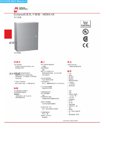
标准
•UL 508类型3R,4,4X和12 •CSA类型3R,4,4X和12 •使 用 符 合
• NEMA 3R, 4, 4X, 12 and 13 •IEC 60529,IP 66
施工
•成立14或16号304或316 不锈钢.
•连续焊缝地面 流畅.
单门机箱
耐腐蚀
壁挂式机箱
芯片中文手册,看全文,戳
Eclipse的系列,不锈钢 - NEMA 4X
单门机箱
304 S.S.
零件号
EN4SD12126SS EN4SD16126SS EN4SD16166SS EN4SD16206SS EN4SD20166SS EN4SD20206SS EN4SD24206SS EN4SD16128SS EN4SD16168SS
外形尺寸
Door/
车身闭锁
A B C Gauge Qty
12.00 12.00 6.00 16
1
16.00 12.00 6.00 16
1
16.00 16.00 6.00 16
1
16.00 20.00 6.00 16
1
20.00 16.00 6.00 16
1
20.00 20.00 6.00 16
1
24.00 20.00 6.00 16
EN4SD30248S16 EN4SD30308S16 EN4SD36248S16 EN4SD36308S16 EN4SD161210S16 EN4SD161610S16 EN4SD162010S16 EN4SD201610S16 EN4SD202010S16 EN4SD202410S16 EN4SD241610S16 EN4SD242010S16 EN4SD242410S16 EN4SD243010S16 EN4SD302010S16 EN4SD302410S16 EN4SD303010S16 EN4SD362410S16 EN4SD363010S16 EN4SD482410S16 EN4SD202012S16 EN4SD242412S16 EN4SD302412S16 EN4SD362412S16 EN4SD363012S16 EN4SD363612S16 EN4SD483616S16R
LTC2440中文资料
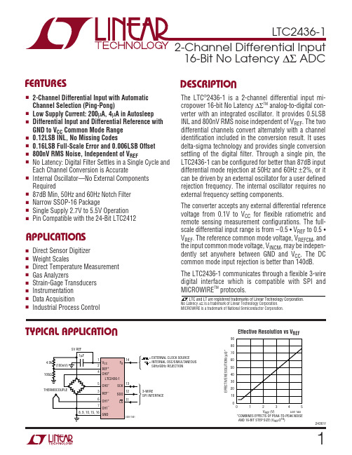
AXI U
RATI GS
U U W PACKAGE/ORDER I FOR ATIO
TOP VIEW VCC REF + REF – CH0+ CH0– CH1+ CH1– GND 1 2 3 4 5 6 7 8 16 GND 15 GND 14 FO 13 SCK 12 SDO 11 CS 10 GND 9 GND
TYPICAL APPLICATIO
5V REF 1µF 4.9k (100mV) 100Ω 1 2 4 VCC
+
EFFECTIVE RESOLUTION (µV)*
FO
14
REF CH0+ LTC2436-1 CH0– REF – CH1
+
= EXTERNAL CLOCK SOURCE = INTERNAL OSC/SIMULTANEOUS 50Hz/60Hz REJECTION
SCK SDO CS
13 12 11 3-WIRE SPI INTERFACE
CH1– GND
24361 TA01
U
Effective Resolution vs VREF
90 80 70 60
U
24361f
1
元器件交易网
AM42DL3244GB40IT资料

— Operating: 22 mA maximum for 70 ns, 30 mA maximum for 55 ns — Standby: 10 µA maximum
■ Ultra low power consumption (typical values)
— Hardware method for detecting program or erase cycle completion
■ Secured Silicon (SecSi) Sector: Extra 256 Byte sector
— Factory locked and identifiable: 16 bytes available for secure, random factory Electronic Serial Number; verifiable as factory locked through autoselect function. — Customer lockable: Sector is one-time programmable. Once locked, data cannot be changed
■ Hardware reset pin (RESET#)
— Hardware method of resetting the internal state machine to reading array data
■ Zero Power Operation
— Sophisticated power management circuits reduce power consumed during inactive periods to nearly zero
HFBR-2412中文资料
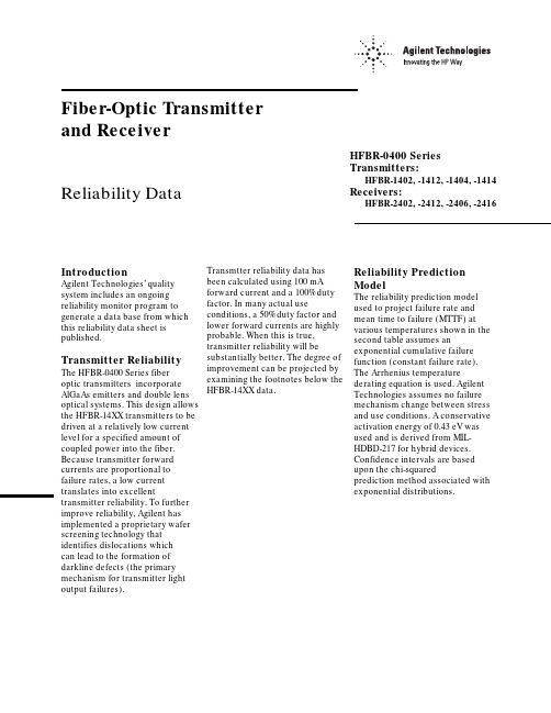
Fiber-Optic Transmitter and ReceiverReliability Data IntroductionAgilent Technologies’ quality system includes an ongoing reliability monitor program to generate a data base from which this reliability data sheet is published.Transmitter Reliability The HFBR-0400 Series fiberoptic transmitters incorporate AlGaAs emitters and double lens optical systems. This design allows the HFBR-14XX transmitters to be driven at a relatively low current level for a specified amount of coupled power into the fiber. Because transmitter forward currents are proportional to failure rates, a low current translates into excellent transmitter reliability. To further improve reliability, Agilent has implemented a proprietary wafer screening technology that identifies dislocations whichcan lead to the formation of darkline defects (the primary mechanism for transmitter light output failures).HFBR-0400 SeriesTransmitters:HFBR-1402, -1412, -1404, -1414Receivers:HFBR-2402, -2412, -2406, -2416 Transmtter reliability data hasbeen calculated using 100 mAforward current and a 100% dutyfactor. In many actual useconditions, a 50% duty factor andlower forward currents are highlyprobable. When this is true,transmitter reliability will besubstantially better. The degree ofimprovement can be projected byexamining the footnotes below theHFBR-14XX data.Reliability PredictionModelThe reliability prediction modelused to project failure rate andmean time to failure (MTTF) atvarious temperatures shown in thesecond table assumes anexponential cumulative failurefunction (constant failure rate).The Arrhenius temperaturederating equation is used. AgilentTechnologies assumes no failuremechanism change between stressand use conditions. A conservativeactivation energy of 0.43 eV wasused and is derived from MIL-HDBD-217 for hybrid devices.Confidence intervals are basedupon the chi-squaredprediction method associated withexponential distributions.Fiber-Optic TransmitterReliability Data HFBR-1402HFBR-1412HFBR-1404HFBR-1414High Temperature Operating Life TestA. Demonstrated PerformanceTest Equivalent Test Condition Samples Device Hours Failures HTOL T A = 85°C, I F = 100 mA880 units879,5003B. Failure CriteriaFailure has occurred when the unitfails catastrophically, or when thelight output power decreases 3 dB.Point Typical PerformancePerformance [1]in Time [2]in Time(90% Confidence) Ambient Junction MTTF [1]FITs [3]MTTF [2]FITs [3] Temperature (°C)Temperature (°C)(hours)(/109 Hours)(hours)(/109 Hours) 85100293,0003411131,00075968095352,0002844158,00063347590424,0002360190,00052557085514,0001947231,00043376580626,0001598281,00035606075766,0001305344,00029055570945,0001059424,000235750651,172,000854526,000190145601,462,000684657,000152340551,838,000544825,000121235502,326,0004301,044,00095830452,965,0003371,331,00075125403,810,0002631,711,000585C. Failure Rate Prediction for Random Failures (I F @ 100 mA, 100% duty cycle)Notes:1. The point MTTF (representing an esti-mate of the mean point MTTF) is the total device hours divided by either the number performance that is expected from 90% ofall samples. This confidence interval isbased on the statistics of the distribution offailure rates prior to the onset of wear out.Refer to MIL-STD-690 for details of thismethodology.Fiber-Optic Link ReceiverReliability DataHFBR-2402HFBR-2412High Temperature Operating Life TestA. Demonstrated PerformanceTest Equivalent Test Condition Samples Device Hours Failures HTOL T A = 85°C, V CC = 5.25 V3,9602,370,0001B. Failure CriteriaFailure has occurred when the unitfails catastrophically. One devicefailed to switch logic states.Point Typical PerformancePerformance [1]in Time [2]in Time(90% Confidence) Ambient Junction MTTF [1]FITs [3]MTTF [2]FITs [3] Temperature (°C)Temperature (°C)(hours)(/109 Hours)(hours)(/109 Hours) 851002,370,000421609,0001,64080952,880,000346742,0001,34075903,530,000282909,0001,09070854,350,0002291,120,00089265805,400,0001841,390,00071960756,740,0001481,730,00057655708,480,0001172,180,000458506510,700,000932,750,000362456013,600,000733,510,000284405517,500,000564,520,000221355022,700,000435,850,000170304529,700,000337,650,000130254039,200,0002510,000,00099C. Failure Rate Prediction, Receiver (V CC = 5.25 V)Notes:1. The point MTTF (representing an esti-mate of the mean point MTTF) is the total device hours divided by either the number performance that is expected from 90% ofall samples. This confidence interval isuseful life failures. Refer to MIL-STD-690 fordetails of this methodology.Fiber-Optic Link ReceiverReliability DataHFBR-2406HFBR-2416High Temperature Operating Life TestA. Demonstrated PerformanceTest Equivalent Test Condition Samples Device Hours Failures HTOL T A = 85°C, V CC = 5.25 V2,2502,250,0000B. Failure CriteriaFailure has occurred when the unitfails catastrophically.Point Typical PerformancePerformance [1]in Time [2]in Time(90% Confidence) Ambient Junction MTTF [1]FITs [3]MTTF [2]FITs [3] Temperature (°C)Temperature (°C)(hours)(/109 Hours)(hours)(/109 Hours) 851002,250,000444977,164102380952,698,5163711,171,95385375903,252,6873071,412,62770870853,941,1732541,711,63358465804,801,4322082,085,24048060755,882,7441702,554,84939155707,250,3821383,148,80831850658,991,4071113,904,927256456011,222,799894,874,010205405514,102,949716,124,846163355017,848,023567,751,315129304522,755,516449,882,616101254029,238,4093412,698,10779C. Failure Rate Prediction, Receiver (V CC = 5.25 V)Notes:1. The point MTTF (representing an esti-mate of the mean point MTTF) is the total device hours divided by either the number performance that is expected from 90% ofall samples. This confidence interval isuseful life failures. Refer to MIL-STD-690 fordetails of this methodology.HFBR-0400 Mechanical and Environmental Test Data [1]MIL-STD-883D Units Total Test Name Reference Test Conditions Tested Failed Temperature Cycle1010500 cycles from -55 to +125°C, 15 minutes20201at extremes, 5 minutes transfer. [1]HFBR-1414500 cycles from -55 to +125°C, 15 minutes20900at extremes, 5 minutes transfer.[1]HFBR-2416 85/85T A = 85°C, 85% relative humidity,21407No bias, duration = 1,000 hours. [1]HFBR-1414T A = 85°C, 85% relative humidity,22206V CC = 5 volts, Duration = 1,000 hours[1]HFBR-2416 High Temperature1008T A = 125°C800 Storage Condition B1000 hoursResistance to2015Three 1 minute immersions.200 Solvents Brush after solvent immersion.Chemical Resistance— 5 minutes in Acetone, Methanol, Freon TF200and Boiling WaterVibration Variable 2007,20 G min., 20 to 2000 Hz.200 Frequency Condition B4, 4 minute cycles each X, Y, and Z.Thermal Shock1011-55°C to +125°C, 15 cycles600Condition B 5 min. dwell / 10 sec. transferMechanical Shock2002, 5 blows each X1, X2, Y1, Y2, Z1, Z2600Condition B1500 G, 0.5 msec. pulse.Port Wear Test [2]T A = 25°C500 connectorings200Less than 1 dBm variationConnector Side T A = 25°C 1 kg side load100 Load [3]Less than 1 dBm variationPort Strength [4]T A = 25°C 6 kg-cm (5.21 inch-lbs), no port damage100 Seal-Dye Penetrant101445 psi, 10 hours200 (Zyglo)Condition D No Leakage into microelectronic cavitySolderability2003245°C300 ESD Method 3015Human body model @ 10,000 V50HFBR-1414Human body model @ 2,000 V50HFBR-2402Human body model @ 1000 V50HFBR-2416Notes: See following page.Notes:1. Devices were preconditioned with 10 second, 260°C solder dip and 20 cycles, -40°C to 85°C, temperature cycle.2. Coupled power measurements were maximized before and after stress in determining the 1 dBm variation for SMA HFBR-0400 products. HFBR-0400 ST products do not require this due to the improved coupling design.3. The Connector Side Load test was only applied to HFBR-0400 SMA products. The Connector Side Load testing required that the housing be held so to prevent the leads from yielding. The load was applied through a SMA connectored fiber optic cable, perpendicular to the port. The product family is designed to limit cable and ferrule damage due to cable loading. The support and active leads should yield before damage to the cable or connector occurs. If extreme mechanical abuse of the cable/ connector is anticipated please contact Agilent’s Application Department for suggestions about mechanical strain relief. Due to the spring loaded feature of the ST connector, HFBR-0400 ST products will experience 1 dBm coupled power variation at a side load of less than 1 kg.4. The Port Strength test was designed to gauge the concerns with hand tightening the connector to the fiber optic port. The limit is set to alevel beyond most reasonable hand fastening loading.5. Package tests are defined as stresses that indicate the environmental strength of the package. Units tested indicate the total number of devices taken from the product family. While not all part numbers have been subjected to each stress, worst case products have been included.。
CLC40-S中文资料
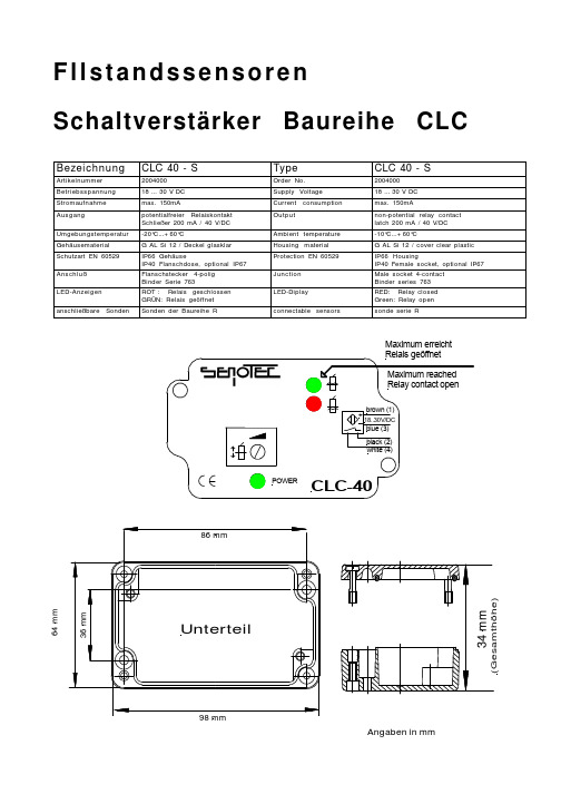
Schaltverstärker Baureihe CLCBezeichnungCLC 40 - STypeCLC 40 - SArtikelnummer 2004000Order No.2004000Betriebsspannung 18 ... 30 V DC Supply Voltage 18 ... 30 V DC Stromaufnahme max. 150mACurrent consumption max. 150mAAusgangpotentialfreier Relaiskontakt Schließer 200 mA / 40 V/DC Outputnon-potential relay contact latch 200 mA / 40 V/DC Umgebungstemperatur -20°C...+60°CAmbient temperature -10°C...+60°CGehäusematerial G AL Si 12 / Deckel glasklar Housing material G AL Si 12 / cover clear plastic Schutzart EN 60529IP66 GehäuseIP40 Flanschdose, optional IP67Protection EN 60529IP66 HousingIP40 Female socket, optional IP67AnschlußFlanschstecker 4-polig Binder Serie 763Junction Male socket 4-contact Binder series 763LED-AnzeigenROT : Relais geschlossen GRÜN: Relais geöffnet LED-DiplayRED: Relay closed Green: Relay open anschließbare SondenSonden der Baureihe Rconnectable sensorssonde serie R64 m mMaximum erreichtSchaltverstärker Baureihe CLCBezeichnungCLC 40 - L05TypeCLC 40 - L05Artikelnummer 2004005Order No.2004005Betriebsspannung 18 ... 30 V DC Supply Voltage 18 ... 30 V DC Stromaufnahme max. 150mACurrent consumption max. 150mAAusgangpotentialfreier Relaiskontakt Schließer 200 mA / 40 V/DC Outputnon-potential relay contact latch 200 mA / 40 V/DC Umgebungstemperatur -20°C...+60°CAmbient temperature -10°C...+60°CGehäusematerial G AL Si 12 / Deckel glasklar Housing material G AL Si 12 / cover clear plastic Schutzart EN 60529IP66 GehäuseIP40 Flanschdose, optional IP67Protection EN 60529IP66 HousingIP40 Female socket, optional IP67Anschlußkabel LIYCY 4x0,25mm² Länge: 0,5m Junction cable LIYCY 4x0,25mm² length: 0,5m LED-AnzeigenROT : Relais geschlossen GRÜN: Relais geöffnet LED-DiplayRED: Relay closed Green: Relay open anschließbare SondenSonden der Baureihe Rconnectable sensorssonde serie R64 m mMaximum erreichtSchaltverstärker Baureihe CLC(64 m mMaximum erreichtBezeichnungCLC 40 - L15TypeCLC 40 - L15Artikelnummer 2004015Order No.2004015Betriebsspannung 18 ... 30 V DC Supply Voltage 18 ... 30 V DC Stromaufnahme max. 150mACurrent consumption max. 150mAAusgangpotentialfreier Relaiskontakt Schließer 200 mA / 40 V/DC Outputnon-potential relay contact latch 200 mA / 40 V/DC Umgebungstemperatur -20°C...+60°CAmbient temperature -10°C...+60°CGehäusematerial G AL Si 12 / Deckel glasklar Housing material G AL Si 12 / cover clear plastic Schutzart EN 60529IP66 GehäuseIP40 Flanschdose, optional IP67Protection EN 60529IP66 HousingIP40 Female socket, optional IP67Anschlußkabel LIYCY 4x0,25mm² Länge: 1,5m Junction cable LIYCY 4x0,25mm² length: 1,5m LED-AnzeigenROT : Relais geschlossen GRÜN: Relais geöffnet LED-DiplayRED: Relay closed Green: Relay open anschließbare SondenSonden der Baureihe Rconnectable sensorssonde serie RSchaltverstärker Baureihe CLC64 m mMaximum erreichtBezeichnungCLC 40 - L50TypeCLC 40 - L50Artikelnummer 2004050Order No.2004050Betriebsspannung 18 ... 30 V DC Supply Voltage 18 ... 30 V DC Stromaufnahme max. 150mACurrent consumption max. 150mAAusgangpotentialfreier Relaiskontakt Schließer 200 mA / 40 V/DC Outputnon-potential relay contact latch 200 mA / 40 V/DC Umgebungstemperatur -20°C...+60°CAmbient temperature -10°C...+60°CGehäusematerial G AL Si 12 / Deckel glasklar Housing material G AL Si 12 / cover clear plastic Schutzart EN 60529IP66 GehäuseIP40 Flanschdose, optional IP67Protection EN 60529IP66 HousingIP40 Female socket, optional IP67Anschlußkabel LIYCY 4x0,25mm² Länge: 5,0m Junction cable LIYCY 4x0,25mm² length: 5,0m LED-AnzeigenROT : Relais geschlossen GRÜN: Relais geöffnet LED-DiplayRED: Relay closed Green: Relay open anschließbare SondenSonden der Baureihe Rconnectable sensorssonde serie R。
RT424012中文资料
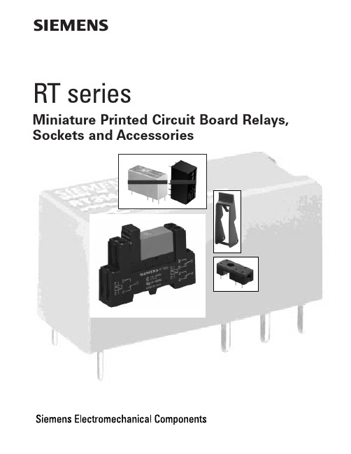
元器件交易网
Ordering Information
Typical Part Number B RT
1
3
1. Basic Series: RT = Miniature, printed circuit board relay.
2. Enclosure: 1 = 1 pole 12A, Pinning 3.5mm, flux-tight (Code 1). 3 = 1 pole 16A, Pinning 5mm, flux-tight (Code 3). 4 = 2 pole 8A, Pinning 5mm, flux-tight (Code 5).
4. Contact Material: 4 = Silver-nickel 90/10 (standard stock).
1 = Silver cadmium Oxide (Special order)
5. Coil Voltage: 005 = 5VDC 006 = 6VDC
009 = 9VDC 012 = 12VDC
Operate Data @ 25°C
Must Operate Voltage(DC): 70% of nominal. Must Release Voltage(DC): 10% of nominal. Operate Time (Excluding Bounce):
7 ms, typ., 15ms max. at nom. voltage. Release Time (Excluding Bounce):
RT series (DC Coil)
16 Amp PC Board Miniature Relay
Meets VDE 10mm Spacing, 5KV Dielectric
佛玛拓 ST 2412 安全技术说明书
安全技术说明书页: 1/10 巴斯夫安全技术说明书按照GB/T 16483编制日期 / 本次修订: 06.03.2022版本: 1.5日期/上次修订: 09.11.2016上次版本: 1.4日期 / 首次编制: 17.09.2013产品: 佛玛拓 ST 2412Product: FoamStar® ST 2412(30535109/SDS_GEN_CN/ZH)印刷日期 02.11.20231. 化学品及企业标识佛玛拓 ST 2412FoamStar® ST 2412推荐用途和限制用途: 消去泡沫公司:巴斯夫(中国)有限公司中国上海浦东江心沙路300号邮政编码 200137电话: +86 21 20391000传真号: +86 21 20394800E-mail地址: **********************紧急联络信息:巴斯夫紧急热线中心(中国)+86 21 5861-1199巴斯夫紧急热线中心(国际):电话: +49 180 2273-112Company:BASF (China) Co., Ltd.300 Jiang Xin Sha RoadPu Dong Shanghai 200137, CHINA Telephone: +86 21 20391000Telefax number: +86 21 20394800E-mail address: ********************** Emergency information:Emergency Call Center (China):+86 21 5861-1199International emergency number: Telephone: +49 180 2273-1122. 危险性概述纯物质和混合物的分类:根据 GHS 标准,该产品不需要进行分类。
巴斯夫安全技术说明书日期 / 本次修订: 06.03.2022版本: 1.5产品: 佛玛拓 ST 2412Product: FoamStar® ST 2412(30535109/SDS_GEN_CN/ZH)印刷日期 02.11.2023标签要素和警示性说明:根据GHS标准,该产品不需要添加危险警示标签其它危害但是不至于归入分类:注意有关存储和操作的规定或注解,无已知特殊危害。
FEC40-24S15中文资料
Model Number Output Voltage Output AmpsInput Range efficiency Ripple & NoiseSINGLe OUTPUTFEC40-24S3P3 3.3 VDC 8 18-36 VDC 50mV Pk-Pk 87% FEC40-48S3P38 36-75 VDC 50mV Pk-Pk 88% FEC40-24S05 5 VDC 8 18-36 VDC 50mV Pk-Pk 89% FEC40-48S058 36-75 VDC 50mV Pk-Pk 90% FEC40-24S12 12 VDC 3.33 18-36 VDC 75mV Pk-Pk 88% FEC40-48S123.33 36-75 VDC 75mV Pk-Pk 89% FEC40-24S15 15 VDC 2.66 18-36 VDC 75mV Pk-Pk 89% FEC40-48S152.66 36-75 VDC 75mV Pk-Pk 89% DUAL OUTPUTFEC40-24D3305 3.3 / 5 VDC 4 / 4 18-36 VDC 100mV Pk-Pk 84% FEC40-48D3305 4 / 4 36-75 VDC 100mV Pk-Pk 85% TRIPLe OUTPUT FEC40-24T3312 3.3, +/-12 VDC 6, +/-0.40 18-36 VDC 50 / 75mV Pk-Pk 85% FEC40-48T33126, +/-0.40 36-75 VDC 50 / 75mV Pk-Pk 86% FEC40-24T3315 3.3, +/-15 VDC 6, +/-0.30 18-36 VDC 50 / 75mV Pk-Pk 85% FEC40-48T33156, +/-0.30 36-75 VDC 50 / 75mV Pk-Pk 86% FEC40-24T0512 5, +/-12 VDC 6, +/-0.40 18-36 VDC 50 / 75mV Pk-Pk 87% FEC40-48T05126, +/-0.40 36-75 VDC 50 / 75mV Pk-Pk 88% FEC40-24T0515 5, +/-15 VDC 6, +/-0.30 18-36 VDC 50 / 75mV Pk-Pk 87% FEC40-48T05156, +/-0.3036-75 VDC50 / 75mV Pk-Pk88%Wide 2 : 1 Input Range High Efficiency Regulated Outputs 1600V Isolation Full EMI Shielding L-C Type Input FilterUnit measures 2.0”W x 2.0”L x 0.4”HINPUT SPecIfIcATIONSInput Voltage Ranges: 24 VDC Nominal 18-36 VDC48 VDC Nominal 36-75 VDC Input Filter (Note 6) L-C TypeUnder Voltage Lockout 24V Input DC-DC On: 17.8VDC-DC Off: 16V48V Input DC-DC On: 36VDC-DC Off: 34V Input Voltage Variation dv/dt 5V / mS, max.(Complies with ETS300 132 part 4.4) Input Surge Voltage 100mS max. 24V Input 50VDC48V Input 100VDC Input Reflected Ripple (Note 7) Nom I/P and FL 40mA Pk-Pk Start Up Time Nom. I/P and Static Resistive Load25mS, typ.Remote ON/OFF (Note 8) DC-DC On: Open or 3.5V < Vr < 12VDC-DC Off: Short or 0V < Vr < 1.2V Remote Off Input Current Nom. Input: 2.5mA OUTPUT SPecIfIcATIONSOutput Power 40 Watts Max.Voltage and Current See Selection ChartO/P Accuracy (FL & Nom I/P) single/dual; +/- 1%Triple Main: +/-1%Triple Aux.: +/-3%Voltage Adjust (Note 1) +/-10%Min. Load-Triple Only (Note 2) 10%Load Regulation-10%-FL singles: +/-0.5%(Note 3) duals: +/-1%Triple Main: +/-2%Triple Aux.: +/-5%Line Regulation single/dual; +/- 0.5%Triple Main: +/-1%Triple Aux.: +/-5%Cross Regulation (Note 4) single/dual/triple main +/-1%triple aux. +/-5%Temperature Coefficient +/-0.02%/DegC, Max.Ripple/Noise (Note 5) See Selection ChartTransient Response (25% Load Step) 400uS Voltage Stability (singles/duals) +/- 2%(triples) 5 V:+/-2%, Aux: +/-5% Over Load Protection FL, Nom. I/P: 150% Max.Short Circuit Protection Hiccup, Auto Recovery OVP Threshold, Zener Diode Clamp:3.3V Output 3.9Volts5V Output 6.2Volts12V Output 15Volts15V Output 18Volts GeNeRAL SPecIfIcATIONSInput-Out Isolation 1600VDCIsolation Resistance 10-9nth OhmsIsolation Capacitance 1000pF, Max.Efficiency See Selection ChartSwitching Frequency (Note 9) 300Khz, typ eNVIRONMeNTAL SPecIfIcATIONSOper. Temperature -40 to +85°C with derate Storage Temperature -55 to +105°C *Relative Humidity 5 to 95% RH *Maximum Case Temp 100°C *Over Temp. Protection 115°C, typ.Thermal Impedance (Note 11) Convection: 9.2°C/WattHeat Sink w. 20LFM 8.5°C/WattHeat Sink w. 500LFM 2.8°C/Watt Thermal Shock MIL-STD-810DVibration 10-55Hz, 2G, 30 Minutesalong X, Y and Z AxesMTBF (Note 10) 1.398 MHrsPHYSIcAL SPecIfIcATIONSCase Material Nickel-Coated CopperNon-Conductive Base Construction Fully Encapsulated withUL94-VO EpoxyDimensions 2.0” x 2.0” x 0.40”Weight 2.11 oz, (60g)*These are stress ratings. Exposure of the devices to any of these conditions may adversely affect long term reliability. Proper operation under conditions other than the standard operating conditions is neither warranteed nor implied. All specifications are typical at nominal input, full load, and 25DegC unless otherwise notedAstrodyne products are not authorized or warranteed for use as critical components in life support systems, equipment used in hazardous environments, nuclear controls systems, or other mission-critical applications.Notes:1. Maximum output deviation is 10% inclusive of remote sense and him. If remote sense is not being used, the +Vsense should be connected to its cor-responding +OUTPUT and likewise the sense should be connected to its corresponding -OUTPUT.2. Triple outputs requires a minimum 10% loading on the output to maintain specified regulation. Operation under no-load condition will not damage these devices, however they may not meet all listed specifications3.Load regulation for triple output:Main output (V1): 10 to 100% with 10% to 100% balanced on auxiliaries.Auxiliary outputs (V2 and V3): 10% to 100% balanced on all outputs.4.Cross regulation for triple output:Main output 100% load, auxiliary 100%, other auxiliary 25% to 100%.Auxiliary outputs (V2 and V3): main output 100% load, auxiliary 100%, other auxiliary 25% to 100% or main output 25%, auxiliary 25%, other auxiliary 25% to 100%.5. The models of FEC40-XXD3305 are specified with a 1uF ceramic output capacitors.6. An external filter capacitor is required for normal operation. The capacitor should be capable of handing 1A ripple current for 48V/24V models. Astrodyne suggests: Nippon chemi-con KMF series, 220µF/100V, ESR 9OmÙ.7. Simulated source impedance of 12uH. 12uH inductor in series with +Vin.8. The ON/OFF control pin voltage is referenced to negative Input.9. Switching frequency for dual output: Master (5Vo) 300KHz; Slave (3.3Vo) 500KHz10. BELLCORE TR-NWT-000332. Case I: 50% Stress, Temperature at 4OºC. (Ground fixed and controlled environment). 11. Heat sink is optional and P/N: 7G-OO26A.12. Any condition of dual output (3.3V/5V) rated lout current, not to exceed 8A of total output currents. 13. Maximum value at nominal input voltage and full load.14. Typical value at nominal input voltage and full load.15.Test by minimum Vin and constant resistor load.MecHANIcAL DIMeNSIONS1. All dimensions in Inches (mm) Tolerance: X.XX Ʋ0.02 (X.X Ʋ0.5)X.XXX Ʋ0.01 (X.XX Ʋ0.25)2. Pin pitch tolerance Ʋ0.014(0.35)8(8)9(9)TRIM UPTRIM DOWNR DexTeRNAL OUTPUT TRIMMINGPin# SingleDualTriple1 +INPUT +INPUT +INPUT2 -INPUT -INPUT -INPUT3 CTRL CTRL CTRL4 NC3.3V+AUX 5 -SENSE (note 1) 3.3V RTN (COM) COMMON 6 +SENSE (note 1) NC -AUX 7 +OUTPUT NC +OUTPUT8 -OUTPUT 5V-OUTPUT (COM) 9TRIM5V RTN (COM)NCOUTPUT DeRATING cURVe606672753654428283INPUT VOLTAGE (V))%( Y C N E I C I F F E FEC40-48S05Efficiency VS Input voltage92919089888786858448 5678126570OUTPUT LOAD (A))%( Y C N E I C I F F E FEC40-48S05Efficiency VS Output load949290888684828075 34FEC40-48S05 Derating Curve50 60 70 80 90 100-40-250-10255075AMBIENT TEMPERATURE (ºC))%( R E W O P T U P T U O。
ZT485ECN中文资料(List Unclassifed)中文数据手册「EasyDatasheet - 矽搜」
ZT4xxE
ZT483E, ZT485E, ZT488E ZT489E, ZT490E, ZT491E
低功率5V 250kbps/ 10MbpsRS485收发器
特征
•达到或超过ANSI斯坦要求 准TIA / EIA-485-A和ISO 8482:1987(E)specifi阳离子欲诉 CC 在+ 5V±5%
Differential Input Voltage, (V ID) ..................... -12V to +12V
A, B (V I) .......................................................... +12V to -7V
DriverCommonModeOutput 有R L =27Ω或50Ω. C L = 50pF.请参看图3.
ChangeinVoltageMagnitude 差分输出电压,带有R forComplimentaryStates,dOVC 指如图1所示.
L =27Ω或50Ω,C L = 50pF.
ChangeinVoltageMagnitude 共模输出电压,带有R forComplimentaryStatesO,VC 请参看图2.
The information furnished by Zywyn has been carefully reviewed for accuracy and reliability. Its application or use, however, is solely the responsibility of the user.否 responsibility of the use of this information become part of the terms and conditions of any subsequent sales agreement with Zywyn.规格若有变更, without the responsibility for any infringement of patents or other rights of third parties which may result from its 使用. No license or proprietary rights are granted by implication or otherwise under any patent or patent rights of Zywyn Corporation.
RP40-2412SG中文资料
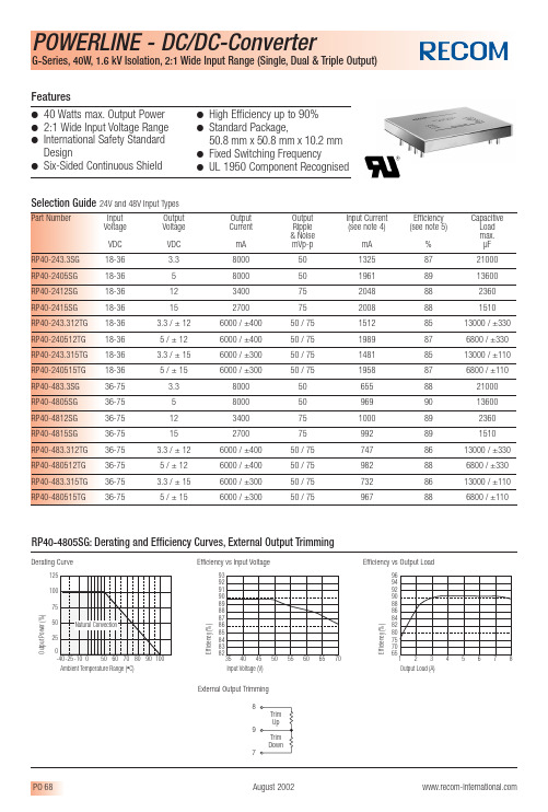
RP40-4805SG:Derating and Efficiency Curves,External Output TrimmingAugust 2002PO Specifications(typical at nominal input and 25°C unless otherwise noted)Output Power40W max. Voltage Accuracy (full Load and nominal Vin)Single / Dual±1%Triple Main±1%Auxilliary±5% Voltage Adjustability (single output only)±10% Minimum Load Voltage (see note 1)Single & Triple10% of FLDual (3.3V)800mA Line Regulation (LL-HL at FL)±0.5% Load Regulation (10% to 100% FL)Single±0.5%Dual±1%Triple Main±2%Auxilliary±5% Ripple and Noise,20MHz BW (measured with a 104pF/50V MLCC) See selection guide table Temperature Coefficient±0.02%/°C max. Transient Response Recovery Time (25% load step change)400µsec Over Voltage Protection (zener diode clamp): 3.3V Output 3.9V5V Output 6.2V12V Output15V15V Output18V Over Load Protection (% of full load at nominal Vin)150% max. Short Circuit Protection Hiccup,Automatic Recovery Input Voltage Range 24V types nominal input18-36VDC48V types nominal input36-75VDC Under Voltage Lockout24V Input DC-DC ON17.8VDCDC-DC OFF16VDC48V Input DC-DC ON36VDCDC-DC OFF34VDC Input Filter L-C Type Input Surge Voltage (100 ms max.)24V Input50VDC48V Input100VDC Input Reflected Ripple (see note 2) Nominal Vin and full load40mAp-p Start Up Time (nominal Vin and constant resistor load)25ms typ. Remote ON/OFF (see note 3)DC-DC ON Open or 3.5V < Vr < 12VDC-DC OFF Short or 0V < Vr < 1.2V Remote off Input Current Nominal Vin 2.5 mA Isolation Voltage1600VDC Isolation Resistance109ΩIsolation Capacitance1000pF Switching Frequency 300kHz Approved to Safety Standards UL 1950,EN60950 Case Material Nickel-Coated Copper Base Material Non-conducted Black FR4 Potting Material Epoxy (UL94-V0) Weight60g (2.11 oz) Dimensions50.8 x 50.8 x 10.2 mm MTBF (MIL-HDBK-217F,TA = 25°C full load) 1.434 x 10⁵Hourscontinued on next page August 2002PO 69August 2002PO 70。
MAX1241中文资料datasheet

MAX1240 / MAX1241 采用 8 引脚封装的低 功耗、12 位模数转换器转换器(ADC)。 MAX1240 采 用 + 2.7V 至 + 3.6V 的 电 源 供 电,MAX1241 采用单电源供电范围是+ 2.7V 至+ 5.25V。这两款设备都具有 7.5μs 的功 能 逐次逼近 ADC,快速跟踪/保持(1.5μs), 片上时钟和高速 3 线串行接口。 在 73ksps 的 最 大 采 样 速 度 下 , 功 耗 仅 为 37mW(VDD = 3V)。2μA 关断模式以较 慢的吞吐率来降低功耗。 MAX1240 具 有 内 部 2.5V 参 考 电 压 , 而 MAX1241 需要外部参考电 压。MAX1241 接受从 0V 到VREF 和参考信号输入范围包括 正电源轨。外部的时钟从 3 线接口访问数据, 它直接连接到标准微控制器的 I/O 港口。该 接口与 SPI™,QSPI™和 MICROWIRE™兼容。 该接卓越的交流特性和极低的功耗,易于使 用和小封装尺寸,使这些转换器成为远程传 感器和数据采集应用的理想之选,或者是要 求降低功耗和对空间有要求的电路的最好 选择。MAX1240/MAX1241 采用 8 引脚 PDIP 和 SO 封装。
兑换率
转换时间 跟踪/保持采集时 间 转换时间 吞吐率 光圈抖动
tCONV
t ACQ
t APR
fSCLK=2.1MHz 图8
5.5
7.5
us
1.5
us
73
ksps
30
ns
<50
ps
模拟输入
输入电压范围 输入电容
0
VREF V
16
pF
电源要求
C2404资料

Product Construction:Conductor:• Fully annealed tinned copper perASTM B-33• Fully annealed solid bare copper perASTM B-3, (C2754, C2755)Insulation:• Premium-grade, coIor-coded S-R PVCper UL 1061Jacket:• PVC, gray• Temperature Range: –20°C to +80°CApplications:• Public address systems• Intercoms• Remote control circuits• Suggested voltage rating: 300 voltsCompliances:• NEC Article 800 Type CM (UL: 75°C)• UL Style 2464 (UL: 80°C 300V)• CSA CMG (CSA: 60°C)• Designed to meet UL 70,000 BTU VerticalTray Flame Test• Passes CSA CMG Flame TestPackaging:• Please contact Customer Service forpackaging and color options*Capacitance between conductorsProduct Construction: Conductor:• 24 AWG fully annealed stranded tinnedcopper per ASTM B-33 Insulation:• Premium-grade, coIor-coded S-R PVCper UL 1061• Color Code: See charts below Jacket:• PVC, gray• Temperature Range: –20°C to +80°C Applications:• Public address systems• Intercoms• Internal telephones• Remote control circuits• Suitable for EIA RS-232 applications • Suggested voltage rating: 300 volts Features:• Easy to terminate• Excellent electrical properties• Tinned conductors provide excellentcorrosion resistance• Assists soldering applications Compliances:• NEC Article 800 Type CM (UL: 75°C)• UL Style 2464 (UL: 80°C, 300V)• UL Style 2576 (UL: 80˚C, 150V)• CSA CMG (CSA: 60°C)• Designed to meet UL 70,000 BTU Vertical Tray Flame Test• Passes CSA CMG Flame Test Packaging:• Please contact Customer Service forpackaging and color optionsProduct Construction:Conductor:• 22 AWG fully annealed, stranded tinnedcopper per ASTM B-33Insulation:• Premium-grade, coIor-coded S-R PVCper UL 1061• Color Code: See charts belowJacket:• PVC, gray• Temperature Range: –20°C to +80˚CApplications:• Public address systems• Intercoms• Internal telephones• Remote control circuits• Suitable for EIA RS-232 applications• Suggested voltage rating: 300 voltsFeatures:• Easy to terminate• Excellent electrical properties• Tinned conductors provide excellentcorrosion resistance• Assists soldering applicationsCompliances:• NEC Article 800 Type CM (UL: 75°C)• UL Style 2464 (UL: 80°C, 300V)• UL Style 2576 (UL: 80˚C, 150V)• CSA CMG (CSA 80°C)• Designed to meet UL 70,000 BTU VerticalTray Flame Test• Passes CSA CMG Flame TestPackaging:• Please contact Customer Service forpackaging and color options†CM-CSA CMG OnlyProduct Construction:Conductor:• 20 or 18 AWG fully annealed stranded,tinned copper per ASTM B-33Insulation:• Premium-grade, coIor-coded PVC perUL 1007• Color Code: See charts belowJacket:• PVC, gray• Temperature Range: –20˚C to +80°CApplications:• Public address systems• Intercoms• Internal telephones• Remote control circuits• Suitable for EIA RS-232 applications• Suggested voltage rating: 300 voltsCompliances:• NEC Article 800 Type CM (UL: 75°C)• UL Style 2464 (UL: 80°C, 300V)• UL Style 2576 (UL: 80˚C, 150V)• CSA CMG (CSA: 60°C)• Designed to meet UL 70,000 BTU VerticalTray Flame Test• Passes CSA CMG Flame TestPackaging:• Please contact Customer Service forpackaging and color options†CM (UL) c(UL), CSA CMG OnlyProduct Construction:Conductor:• 16 thru 12 AWG fully annealed strandedtinned copper per ASTM B-33Insulation:• Premium-grade, coIor-coded PVC• Color Code: See chart belowJacket:• PVC, gray• Temperature Range: –20°C to +80°CApplications:• Public address systems• Intercoms• Internal telephones• Remote control circuits• Suitable for EIA RS-232 applications• Suggested voltage rating: 300 voltsCompliances:• NEC Article 725 Type CL3 (UL: 75°C)• NEC Article 800 Type CM (UL: 75°C)• UL Style 2464 (UL: 80°C, 300V)• UL Style 2587 (UL: 90°C, 600V)• CSA CMG (CSA: 60°C)• Designed to meet UL 70,000 BTU VerticalTray Flame Test• Passes CSA CMG Flame TestPackaging:• Please contact Customer Service forpackaging and color options†CL3, UL2587, CSA CMH OnlyProduct Construction: Conductor:• 22 thru 18 fully annealed stranded tinnedcopper per ASTM B-33Insulation:• Premium-grade, coIor-coded PVC (18 AWG), S-R PVC (22 AWG)• Color Code: See chart belowJacket:• PVC, gray• Temperature Range: –20°C to +80°C Applications:• TV antenna rotor control• Satellite actuator control• Public address systems• Suggested voltage rating: 300 volts Features:• Tinned copper conductors provide excellent corrosion resistance• Assists with soldering applications Compliances:• NEC Article 800 Type CM (UL: 75°C)• UL Style 2464 (UL: 80°C, 300V)• CSA CMG (CSA: 60°C)• Designed to meet UL 70,000 BTU VerticalTray Flame Test• Passes CSA CMG Flame Test Packaging:• Please contact Customer Service forpackaging and color options。
IRS20124S中文资料

D IGIT AL A UDIO D RIVER WITH D ISCRETE D EAD -TIME AND P ROTECTIONProduct SummaryV SUPPL Y 200V max.I O +/-1A / 1.2A typ.Selectable Dead Time15/25/35/45ns typ.Prop Delay Time 70ns typ.Bi-directional Over Current SensingFeatures•200V high voltage ratings deliver up to 1000Woutput power in Class D audio amplifier applications•Integrated dead-time generation and bi-directional over current sensing simplify design•Programmable compensated preset dead-time for improved THD performances over temperature •High noise immunity•Shutdown function protects devices from overload conditionsIRS20124S(PbF)SymbolDefinitionMin.Max.UnitsV B High side floating supply voltage -0.3220V V s High side floating supply voltage VB-20VB+0.3V V HO High side floating output voltage Vs-0.3VB+0.3V V CC Low side fixed supply voltage -0.320V V LO Low side output voltage -0.3Vcc+0.3V V IN Input voltage-0.3Vcc+0.3V V OC OC pin input voltage-0.3Vcc+0.3V V OCSET1 OCSET1 pin input voltage -0.3Vcc+0.3V V OCSET2OCSET2 pin input voltage-0.3Vcc+0.3V dVs/dt Allowable Vs voltage slew rate-50V/ns Pd Maximum power dissipation- 1.25W Rth JA Thermal resistance, Junction to ambient -100°C/W T J Junction Temperature -150°C T S Storage Temperature-55150°CT LLead temperature (Soldering, 10 seconds)-300°CAbsolute Maximum RatingsAbsolute maximum ratings indicate sustained limits beyond which damage to the device may occur. All voltage parameters are absolute voltages referenced to COM. All currents are defined positive into any lead. The thermal resistance and power dissipation ratings are measured under board mounted and still air conditions.DescriptionThe IRS20124S is a high voltage, high speed power MOSFET driver with internal dead-time and shutdown functions specially designed for Class D audio amplifier applications.The internal dead time generation block provides accurate gate switch timing and enables tight dead-time settings for better THD performances.In order to maximize other audio performance characteristics, all switching times are designed for immunity from external disturbances such as VCC perturbation and incoming switching noise on the DT pin. Logic inputs are compatible with LSTTL output or standard CMOS down to 3.0V without speed degradation. The output drivers feature high current buffers capable of sourcing 1.0A and sinking 1.2A. Internal delays are optimized to achieve minimal dead-time variations. Proprietary HVIC and latch immune CMOS technologies guarantee operation down to Vs= –4V, providing outstanding capabilities of latch and surge immunities with rugged monolithic construction.Recommended Operating ConditionsFor Proper operation, the device should be used within the recommended conditions. The Vs and COM offset ratings are tested with all supplies biased at 15V differential.Symbol Definition Min.Max.Units V B High side floating supply absolute voltage Vs+10Vs+18V V S High side floating supply offset voltage Note 1200VV V HO High side floating output voltage Vs VB V CC Low side fixed supply voltage1018V V LO Low side output voltage0VCC V V IN Logic input voltage0VCC V V OC OC pin input voltage0VCC V V OCSET1OCSET1 pin input voltage0VCC V V OCSET2OCSET2 pin input voltage0VCC V T A Ambient Temperature-40125°CDynamic Electrical CharacteristicsV BIAS (V CC, V BS) = 15V, C L = 1nF and T A = 25°C unless otherwise specified. Figure 2 shows the timing definitions.IRS20124S(PbF)Lead DefinitionsSymbol DescriptionVCC Low side logic Supply voltage VB High side floating supply HO High side outputVS High side floating supply returnINLogic input for high and low side gate driver outputs (HO and LO), in phase with HODT/SD Input for programmable dead-time, referenced to COM. Shutdown LO and HO when tied to COM COM Low side supply returnLO Low side outputOC Over current output (negative logic)OC SET1Input for setting negative over current threshold OC SET2Input for setting positive over current thresholdIRS20124S(PbF)VBHOVSO O C S E T O C S E T VccLOCOM50%50%t off(L)t on(L)90%10%90%10%DT HO-LOt off(H)INHOLOt on(H)DT LO-HO DT/SDHO LOV SDT SD90%Figure 1. Switching Time Waveform DefinitionsFigure 2. Shutdown Waveform DefinitionsIRS20124S(PbF)toc filt HIGHVSOCV soct COMCOMtwocVSOCV Soc+tdocCOM COMLOV Soc-15V Vsoc+Vsoc-OCVsoc+Vsoc-COM VSOCFigure 5. OC Waveform DefinitionsFigure 3. OC Input FilterTime DefinitionsIRS20124S(PbF)IRS20124S(PbF)2.0()2()IRS20124S(PbF)2430()()IRS20124S(PbF)10()10()IRS20124S(PbF)IRS20124S(PbF)Figure 6. Effective Dead-timeA longer dead time period is required for a MOSFETwith a larger gate charge value because of thelonger tf. A shorter effective dead-time setting isalways beneficial to achieve better linearity in theClass D switching stage. However, the likelihoodof shoot-through current increases with narrowerdead-time settings in mass production. Negativevalues of effective dead-time may cause excessiveheat dissipation in the MOSFETs, potentiallyleading to their serious damage. To calculate theoptimal dead-time in a given application, the falltime tf for both output voltages, HO and LO, in theactual circuit needs to be measured. In addition,the effective dead-time can also vary withtemperature and device parameter variations.Therefore, a minimum effective dead-time of 10nSis recommended to avoid shoot-through currentover the range of operating temperatures andsupply voltages.V DT Dead-timeFigure 7. Dead-time Settings vs V DT Voltage Design ExampleT able 1 shows suggested values of resistance for setting the dead-time. Resistors withup to 5% tolerancecan be used if theselisted values are fol-lowed.Table 1. Suggested resistor values for dead-timesettingsShutdownSince IRS20124 has internal dead-time genera-tion, independent inputs for HO and LO are no longer provided. Shutdown mode is the only way to turn off both MOSFETs simultaneously to pro-tect them from over current conditions. If the DT/ SD pin detects an input voltage below the thresh-old, VDT4,the IRS20124 will output 0V at both HO and LO outputs, forcing the switching output node to go into a high impedance state.Over Current SensingIn order to protect the power MOSFET, IRS20124 has a feature to detect over current conditions, which can occur when speaker wires are shorted together. The over current shutdown feature can be configured by combining the current sensing function with the shutdown mode via the DT/SD pin.Load Current Direction in Class D Audio ApplicationIn a Class D audio amplifier, the direction of the load current alternates according to the audio in-put signal. An over current condition can therefore happen during either a positive current cycle or a negative current cycle. Fig.9 shows the rela-Figure 8. External ResistorIRS20124S(PbF)Bi-directional Current SensingIRS20124 has an over current detection function utilizing R DS(ON) of the low side switch as a current sensing shunt resistor. Due to the proprietary HVIC process, the IRS20124 is able to sense negative as well as positive current flow, enabling bi-direc-tional load current sensing without the need for any additional external passive components.Figure 9. Direction in MMOSFET Current and LoadCurrentv sVsoc +Vsoc -COM (a ) Normal OperationCondition (b ) Over -Current in Positive Load Current (c ) Over -Current in Negative Load CurrentFigure 10. Vs Waveform in Over-current ConditionIRS20124 measures the current during the period when the low side MOSFET is turned on. Fig.10illustrates how an excessive voltage at Vs node detects an over current condition. Under normal operating conditions, Vs voltage for the low side switch is well within the trip threshold boundaries,V SOC- and V SOC+. In the case of Fig.9(b) which dem-onstrates the amplifier sourcing too much current to the load, the Vs node is found below the trip level, V SOC-. In Fig.9(c) with opposite current direc-tion, the amplifier sinks too much current from the load, positioning Vs well above trip level, V SOC+.Once the voltage in Vs exceeds the preset thresh-old, the OC pin pulls down to COM to detect an over current condition.Since the switching waveform usually contains over/under shoot and associated oscillatory arti-facts on their transient edges, a 200ns blanking interval is inserted in the Vs voltage sensing block at the instant the low side switch is engaged.Because of this blanking interval, the OC function will be unable to detect over current conditions if the low side ON duration less than 200ns.OCFigure 11. Simplified Functional Block Diagram ofBi-Directional Current SensingAs shown in Fig.11, bi-directional current sens-ing block has an internal 2.0V level shifter feeding the signal to the comparator. OC SET1 sets the posi-tive side threshold, and is given a trip level at V SOC+,which is OC SET1 - 2.0V. In same way, for a given OC SET2, V SOC- is set at OC SET2 – 2.0VHow to set OC ThresholdThe positive and negative trip thresholds for bi-directional current sensing are set by the voltages at OC SET1 and OC SET2. Fig.14 shows a typical re-sistor voltage divider that can. be used to set OC SET1 and OC SET2.The trip threshold voltages, V SOC+ and V SOC+, are determined by the required trip current levels, I TRIP+and I TRIP-, and R DS(ON) in the low side MOSFET .Since the sensed voltage of Vs is shifted up by 2.21V internally and compared with the voltages fed to the OC SET1 and OC SET2 pins, the required value of OC SET1 with respect to COM is V OCSET1 = V SOC+ + 2.21 = I TRIP+ x R DS(ON) + 2.21The same relation holds between OC SET2 and V SOC-,V OCSET2 = V SOC- + 2.21 = I TRIP- x R DS(ON) + 2.21In general, R DS(ON) has a positive temperature co-efficient that needs to be considered when thethreshold level is being set. Please also note that,in the negative load current direction, the sensing voltage at the Vs node is limited by the body di-ode of the low side MOSFET as explained later.Design ExampleThis example demonstrates how to use the ex-ternal? resistor network to set I TRIP+ and I TRIP- to be ±11A, using a MOSFET that has R DS(ON)=60mÙ.V ISET1 = V TH + + 2.21 = I TRIP+ x R DS(ON) + 2.21= 11x 60mÙ +2.21 = 2.87VV ISET2 = V TH- + 2.21 = I TRIP- x R DS(ON) + 2.21= (-11)x 60mÙ +2.21 = 1.55VThe total resistance of resistor network is based on the voltage at the Vcc and required bias cur-rent in this resistor network.R total =R3 + R4 + R5 = Vcc / I bias = 12V / 1mA = 12KÙThe expected voltage across R3 is Vcc- V ISET1= 12-2.87=9.13V. Similarly, the voltages across R4 is V SOC+ - V SOC- = 2.87-1.55=1.32V, and the voltage across R5 is V ISET2= 1.55V respectively.R3 =9.13V/ I bias = 9.13KÙR4 =1.32V/ I bias = 1.32KÙR5 =1.55V/ I bias = 1.55KÙChoose R3= 9.09KÙ, R4=1.33KÙ, R5=1.54KÙfrom E-96 series.Consequently, actual threshold levels are V SOC+ =2.88V gives I TRIP+ = 11.2A V SOC- =1.55V gives I TRIP- = -11.0AResisters with 1% tolerances are recommended.IRS20124S(PbF)OC Output SignalThe OC pin is a 20V open drain output. The OC pin is pulled down to ground when an over current condition is detected. A single external pull-up resistor can be shared by multiple IRS20124 OC pins to form the ORing logic. In order for a micro-processor to read the OC signal, this information is buffered with a mono stable multi vibrator to ensure 100ns minimum pulse width.Because of unpredictable logic status of the OC pin, the OC signal should be ignored during power up/down.Limitation from Body Diode in MOSFET When a Class D stage outputs a positive current,flowing from the Class D amp to the load, the body diode of the MOSFET will turn on when the Drain to Source voltage of the MOSFET become larger than the diode forward drop voltage. In such a case, the sensing voltage at the Vs pin of the IRS20124 is clamped by the body diode. This means that the effective Rds(on) is now much lower than expected from Rds(on) of the MOSFET,and the Vs node my not able to reach the thresh-old to turn the OC output on before the MOSFET fails. Therefore, the region where body diode clamping takes a place should be avoided when setting V SOC-.Voltage in Vsbe For further application information for gate driver IC please refer to AN-978 and DT98-2a. For fur-ther application information for class D applica-tion, please refer to AN-1070 and AN-1071.Figure 13. Body Diode in MOSFET Clamps vsVoltage。
口炎清颗粒提取和制粒工艺优选[权威资料]
![口炎清颗粒提取和制粒工艺优选[权威资料]](https://img.taocdn.com/s3/m/3ddb21d15ebfc77da26925c52cc58bd63186931d.png)
口炎清颗粒提取和制粒工艺优选摘要:目的优选口炎清颗粒的提取和制粒工艺。
方法采用高效液相色谱法测定口炎清浸膏中芍药苷含量。
以浸膏收率、芍药苷提取率为评价指标,用单因素试验和正交试验优化提取工艺。
以吸湿率、堆密度、休止角为评价指标,采用多因素比较法和正交试验优化制粒工艺,并测定口炎清颗粒的临界相对湿度。
结果最佳提取工艺为12倍60%乙醇回流提取3次,每次2 h。
口炎清浸膏粉与糊精按6∶4比例混合后用90%乙醇制粒,制得的口炎清颗粒吸湿性小,流动性好,临界相对湿度约为63%。
结论口炎清颗粒的提取和制粒工艺合理可行,稳定性好,可为工业化生产提供依据。
关键词:口炎清颗粒;高效液相色谱法;提取工艺;正交试验;制粒工艺R283.5 A 1005-5304(2013)04-0060-05口炎清颗粒为本院开发的中药汤剂,由赤芍、葛根、石斛、麦冬等组成,功效清热凉血、生津养阴,用于扁平苔藓等口腔疾病的治疗。
汤剂味苦,患者依从性差,且久储易酸败,不易携带,为此,我们将其制成胶囊剂。
为保证制剂质量,合理制定制备工艺,本试验对提取和制粒工艺进行优选。
1 仪器与试药Agilent 1200高效液相色谱仪(美国Agilent公司), HWS24型电热恒温水浴锅(上海科技一恒有限公司),RE-2000A型旋转蒸发仪(上海亚荣生化仪器厂),CS101-2ABN型电热鼓风干燥箱(重庆市永生实验仪器厂),KQ5200型超声波清洗器(昆山市超声仪器有限公司),BS224S电子天平(德国 Sartorius公司)。
口炎清颗粒处方药材购于重庆桐君阁中药材批发公司,经重庆医科大学药学院刘新教授鉴定为正品,均符合2010年版《中华人民共和国药典》(一部)项下有关规定。
芍药苷对照品(批号110736-201136,中国食品药品检定研究院),淀粉(批号20120201,曲阜市药用辅料有限公司),乳糖(批号20120101,湖南尔康药用辅料有限公司),糊精(批号20120301,曲阜市药用辅料有限公司),乙腈为色谱纯,其他试剂均为分析纯。
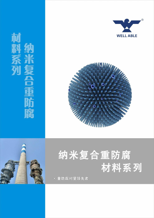
纳米复合重防腐材料系列产品说明书-石狮华宝新材料
超强耐化学腐蚀性
解决衬层“返锈”、 剥离、脱落、溶胀 纳米级及抗开腐裂蚀介质 解决衬层“返锈”、 剥离、脱落、溶胀 解决返及锈开剥裂离脱落 解决衬层“返锈”、 剥离、脱落、溶胀
及开裂
水中固化性能
解决衬层“返锈”、 剥离、脱落、溶胀
优异及机开械裂性能 解决衬层“返锈”、 剥离、脱落、溶胀
优异及基开材附裂着力 解决衬层“返锈”、 剥离、脱落、溶胀
合 计:28.5kg/套 · 适用于常规重防腐体系衬里
A 组分:20kg/桶 · 耐酸、碱、盐、微生物等重腐蚀
B 组分:5kg/桶
· 涂层坚韧、耐磨损、耐冲击
C 组分:30kg/桶 · 无溶剂型
合 计:55kg/套 · 适用于常规重防腐体系衬里
WA82-58
WA72-58 其他型号
水中固化纳米涂料 水中固化纳米胶泥
实验仪器
干混凝土
湿混凝土
基材
底涂
8231A
8241A
环氧树脂 乙烯基树脂
8231C
(kgf/cm2) (kgf/cm2) (kgf/cm2) (kgf/cm2) (kgf/cm2)
铁板-铁板(Q235)
152-161
115-127
铝板-铝板
102-107
76-95
铜板-铜板
195-206
148-167
2.5-3.0
2.7-3.5
弯曲强度(MPa)
140-150
130-140
120-130
耐温性能(℃)
100-120
140-160
耐腐蚀性能
1000多种化学品腐蚀体系,详见耐腐蚀数据表
* 以上为实验测试典型数据,仅供参考,不可作为标准。
离子检验试剂

阳离子铯离子Cs +:四碘合铋酸钾(KBiI 4):与铯离子反应生成亮红色Cs 3[Bi 2I 9]沉淀,用于分析化学试剂,可鉴定铯离子。
铵根离子NH 4+:碘化汞钾(K 2HgI 4): 与氨作用产生黄色或棕色(高浓度时)沉淀,是鉴定试样中氨的常用试剂.灵敏度大约为0。
3μg NH 3/2μL 。
检出限量:0。
05μg 最低浓度:1μg·g —1(1ppm) NH 4++2[HgI 4]2—+4OH — →HgO·Hg(NH 2)I ↓+7I - +3H 2O注:Fe 3+、Cr 3+、Co 2+、Ni 2+、Ag +、Hg 2+等离子能与奈斯勒试剂生成有色沉淀,大量S 2—的存在,使[HgI 4]2-分解析出HgS ↓。
大量I —存在使反应向左进行,沉淀溶解。
妨碍鉴定。
氢氧化钠(NaOH ):在强碱性介质中NH 4++NaOH →NH 3↑+H 2ONH 3使润湿的红色石蕊试纸变蓝或PH 试纸呈碱性反应注:CN -+H2O →OH-并加热HCOO —+NH 3↑干扰鉴定锂离子Li +:高碘酸铁钾(K 2FeIO 6): 与锂离子反应生成黄色的KLi [FeIO 6]沉淀,用作分析化学中鉴定锂离子的试剂。
可由铁离子与高碘酸根反应,调节pH 制得.铁离子Fe 3+:硫氰酸钾(KSCN): 遇Fe 3+ 生成血红色的硫氰酸铁络离子[Fe (SCN )n ]3—n (n=1—6),是检验 Fe 3+ 离子十分灵敏的方法,可以排除目前已知的一切其它金属离子的影响. 注: 1、在酸性溶液中进行,但不能用HNO 3。
2、F —、H 3PO 4、H 2C 2O 4、酒石酸、柠檬酸以及含有α — 或β —羟基的有机酸都能与Fe 3+形成稳定的配合物而干扰。
溶液中若有大量汞盐,由于形成[Hg(SCN )4]2-而干扰,钴、镍、铬和铜盐因离子有色,或因与SCN -的反应产物的颜色而降低检出Fe 3+的灵敏度。
- 1、下载文档前请自行甄别文档内容的完整性,平台不提供额外的编辑、内容补充、找答案等附加服务。
- 2、"仅部分预览"的文档,不可在线预览部分如存在完整性等问题,可反馈申请退款(可完整预览的文档不适用该条件!)。
- 3、如文档侵犯您的权益,请联系客服反馈,我们会尽快为您处理(人工客服工作时间:9:00-18:30)。
Model Number Output Voltage Output AmpsInput Range efficiency Ripple & NoiseSINGLe OUTPUTFEC40-24S3P3 3.3 VDC 8 18-36 VDC 50mV Pk-Pk 87% FEC40-48S3P38 36-75 VDC 50mV Pk-Pk 88% FEC40-24S05 5 VDC 8 18-36 VDC 50mV Pk-Pk 89% FEC40-48S058 36-75 VDC 50mV Pk-Pk 90% FEC40-24S12 12 VDC 3.33 18-36 VDC 75mV Pk-Pk 88% FEC40-48S123.33 36-75 VDC 75mV Pk-Pk 89% FEC40-24S15 15 VDC 2.66 18-36 VDC 75mV Pk-Pk 89% FEC40-48S152.66 36-75 VDC 75mV Pk-Pk 89% DUAL OUTPUTFEC40-24D3305 3.3 / 5 VDC 4 / 4 18-36 VDC 100mV Pk-Pk 84% FEC40-48D3305 4 / 4 36-75 VDC 100mV Pk-Pk 85% TRIPLe OUTPUT FEC40-24T3312 3.3, +/-12 VDC 6, +/-0.40 18-36 VDC 50 / 75mV Pk-Pk 85% FEC40-48T33126, +/-0.40 36-75 VDC 50 / 75mV Pk-Pk 86% FEC40-24T3315 3.3, +/-15 VDC 6, +/-0.30 18-36 VDC 50 / 75mV Pk-Pk 85% FEC40-48T33156, +/-0.30 36-75 VDC 50 / 75mV Pk-Pk 86% FEC40-24T0512 5, +/-12 VDC 6, +/-0.40 18-36 VDC 50 / 75mV Pk-Pk 87% FEC40-48T05126, +/-0.40 36-75 VDC 50 / 75mV Pk-Pk 88% FEC40-24T0515 5, +/-15 VDC 6, +/-0.30 18-36 VDC 50 / 75mV Pk-Pk 87% FEC40-48T05156, +/-0.3036-75 VDC50 / 75mV Pk-Pk88%Wide 2 : 1 Input Range High Efficiency Regulated Outputs 1600V Isolation Full EMI Shielding L-C Type Input FilterUnit measures 2.0”W x 2.0”L x 0.4”HINPUT SPecIfIcATIONSInput Voltage Ranges: 24 VDC Nominal 18-36 VDC48 VDC Nominal 36-75 VDC Input Filter (Note 6) L-C TypeUnder Voltage Lockout 24V Input DC-DC On: 17.8VDC-DC Off: 16V48V Input DC-DC On: 36VDC-DC Off: 34V Input Voltage Variation dv/dt 5V / mS, max.(Complies with ETS300 132 part 4.4) Input Surge Voltage 100mS max. 24V Input 50VDC48V Input 100VDC Input Reflected Ripple (Note 7) Nom I/P and FL 40mA Pk-Pk Start Up Time Nom. I/P and Static Resistive Load25mS, typ.Remote ON/OFF (Note 8) DC-DC On: Open or 3.5V < Vr < 12VDC-DC Off: Short or 0V < Vr < 1.2V Remote Off Input Current Nom. Input: 2.5mA OUTPUT SPecIfIcATIONSOutput Power 40 Watts Max.Voltage and Current See Selection ChartO/P Accuracy (FL & Nom I/P) single/dual; +/- 1%Triple Main: +/-1%Triple Aux.: +/-3%Voltage Adjust (Note 1) +/-10%Min. Load-Triple Only (Note 2) 10%Load Regulation-10%-FL singles: +/-0.5%(Note 3) duals: +/-1%Triple Main: +/-2%Triple Aux.: +/-5%Line Regulation single/dual; +/- 0.5%Triple Main: +/-1%Triple Aux.: +/-5%Cross Regulation (Note 4) single/dual/triple main +/-1%triple aux. +/-5%Temperature Coefficient +/-0.02%/DegC, Max.Ripple/Noise (Note 5) See Selection ChartTransient Response (25% Load Step) 400uS Voltage Stability (singles/duals) +/- 2%(triples) 5 V:+/-2%, Aux: +/-5% Over Load Protection FL, Nom. I/P: 150% Max.Short Circuit Protection Hiccup, Auto Recovery OVP Threshold, Zener Diode Clamp:3.3V Output 3.9Volts5V Output 6.2Volts12V Output 15Volts15V Output 18Volts GeNeRAL SPecIfIcATIONSInput-Out Isolation 1600VDCIsolation Resistance 10-9nth OhmsIsolation Capacitance 1000pF, Max.Efficiency See Selection ChartSwitching Frequency (Note 9) 300Khz, typ eNVIRONMeNTAL SPecIfIcATIONSOper. Temperature -40 to +85°C with derate Storage Temperature -55 to +105°C *Relative Humidity 5 to 95% RH *Maximum Case Temp 100°C *Over Temp. Protection 115°C, typ.Thermal Impedance (Note 11) Convection: 9.2°C/WattHeat Sink w. 20LFM 8.5°C/WattHeat Sink w. 500LFM 2.8°C/Watt Thermal Shock MIL-STD-810DVibration 10-55Hz, 2G, 30 Minutesalong X, Y and Z AxesMTBF (Note 10) 1.398 MHrsPHYSIcAL SPecIfIcATIONSCase Material Nickel-Coated CopperNon-Conductive Base Construction Fully Encapsulated withUL94-VO EpoxyDimensions 2.0” x 2.0” x 0.40”Weight 2.11 oz, (60g)*These are stress ratings. Exposure of the devices to any of these conditions may adversely affect long term reliability. Proper operation under conditions other than the standard operating conditions is neither warranteed nor implied. All specifications are typical at nominal input, full load, and 25DegC unless otherwise notedAstrodyne products are not authorized or warranteed for use as critical components in life support systems, equipment used in hazardous environments, nuclear controls systems, or other mission-critical applications.Notes:1. Maximum output deviation is 10% inclusive of remote sense and him. If remote sense is not being used, the +Vsense should be connected to its cor-responding +OUTPUT and likewise the sense should be connected to its corresponding -OUTPUT.2. Triple outputs requires a minimum 10% loading on the output to maintain specified regulation. Operation under no-load condition will not damage these devices, however they may not meet all listed specifications3.Load regulation for triple output:Main output (V1): 10 to 100% with 10% to 100% balanced on auxiliaries.Auxiliary outputs (V2 and V3): 10% to 100% balanced on all outputs.4.Cross regulation for triple output:Main output 100% load, auxiliary 100%, other auxiliary 25% to 100%.Auxiliary outputs (V2 and V3): main output 100% load, auxiliary 100%, other auxiliary 25% to 100% or main output 25%, auxiliary 25%, other auxiliary 25% to 100%.5. The models of FEC40-XXD3305 are specified with a 1uF ceramic output capacitors.6. An external filter capacitor is required for normal operation. The capacitor should be capable of handing 1A ripple current for 48V/24V models. Astrodyne suggests: Nippon chemi-con KMF series, 220µF/100V, ESR 9OmÙ.7. Simulated source impedance of 12uH. 12uH inductor in series with +Vin.8. The ON/OFF control pin voltage is referenced to negative Input.9. Switching frequency for dual output: Master (5Vo) 300KHz; Slave (3.3Vo) 500KHz10. BELLCORE TR-NWT-000332. Case I: 50% Stress, Temperature at 4OºC. (Ground fixed and controlled environment). 11. Heat sink is optional and P/N: 7G-OO26A.12. Any condition of dual output (3.3V/5V) rated lout current, not to exceed 8A of total output currents. 13. Maximum value at nominal input voltage and full load.14. Typical value at nominal input voltage and full load.15.Test by minimum Vin and constant resistor load.MecHANIcAL DIMeNSIONS1. All dimensions in Inches (mm) Tolerance: X.XX Ʋ0.02 (X.X Ʋ0.5)X.XXX Ʋ0.01 (X.XX Ʋ0.25)2. Pin pitch tolerance Ʋ0.014(0.35)8(8)9(9)TRIM UPTRIM DOWNR DexTeRNAL OUTPUT TRIMMINGPin# SingleDualTriple1 +INPUT +INPUT +INPUT2 -INPUT -INPUT -INPUT3 CTRL CTRL CTRL4 NC3.3V+AUX 5 -SENSE (note 1) 3.3V RTN (COM) COMMON 6 +SENSE (note 1) NC -AUX 7 +OUTPUT NC +OUTPUT8 -OUTPUT 5V-OUTPUT (COM) 9TRIM5V RTN (COM)NCOUTPUT DeRATING cURVe606672753654428283INPUT VOLTAGE (V))%( Y C N E I C I F F E FEC40-48S05Efficiency VS Input voltage92919089888786858448 5678126570OUTPUT LOAD (A))%( Y C N E I C I F F E FEC40-48S05Efficiency VS Output load949290888684828075 34FEC40-48S05 Derating Curve50 60 70 80 90 100-40-250-10255075AMBIENT TEMPERATURE (ºC))%( R E W O P T U P T U O。