IPB50R199CP中文资料
1585LC类别5e网线,4双,U UTP,LC,CMP商品说明书
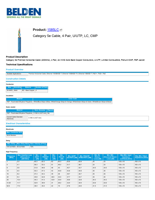
Product:1585LCCategory 5e Cable, 4 Pair, U/UTP, LC, CMPProduct DescriptionCategory 5e Premise Horizontal Cable (200MHz), 4 Pair, 24 AWG Solid Bare Copper Conductors, U/UTP, Limited Combustible, Plenum-CMP, FEP Jacket Technical SpecificationsProduct OverviewConstruction DetailsConductorInsulationOuter JacketElectrical CharacteristicsElectricalsDelayHigh Frequency10022.035.332.31410.323.820.820.120.1100 ± 15100 ± 1515528.132.529.5 4.4 1.419.916.915.8100 ± 25100 ± 15 2003230.827.84117.714.715100 ± 25100 ± 15VoltageUL Voltage Rating300 V (CMP)Mechanical CharacteristicsTemperatureOperating Installation Storage-40°C To +150°C0°C To +50°C-20°C To +75°CBend RadiusStationary Min.Installation Min.1 in (25 mm) 1.8 in (46 mm)Max. Pull Tension:35 lbs (16 kg)Bulk Cable Weight:21 lbs/1000ft (31 kg/km)Standards and ComplianceEnvironmental Suitability:Plenum, IndoorFlammability / Reaction toNFPA 262 Plenum Flame Test (UL910),UL723 (NFPA 255), FT6, FT6, IEC 60332-1-2Fire:CPR Compliance:CPR Euroclass: Eca; CPR UKCA Class: EcaNEC / UL Compliance:Article 800, CMPCEC / C(UL) Compliance:CMPIEEE Compliance:IEEE 802.3bt Type 1, Type 2, Type 3Data Category:Category 5eTIA/EIA Compliance:ANSI/TIA-568.2-D Category 5eISO/IEC Compliance:ISO/IEC 11801-1, IEC 61156-5European DirectiveEU CE Mark, EU Directive 2015/863/EU (RoHS 2 amendment), REACH, EU Directive 2011/65/EU (RoHS 2), EU Directive 2012/19/EU (WEEE), REACH: 2020-01-16 Compliance:UK Regulation Compliance:UKCA MarkAPAC Compliance:China RoHS II (GB/T 26572-2011)Plenum Number:1585ANon-Plenum Number:1583AProduct NotesNotes:Electrical values are expected performance based on cable testing and representative performance within a typical Belden system. Jacket sequentially marked at 2 ft. intervals.Thrid party verified to ANSI/TIA-568-C.2, Category 5e.HistoryUpdate and Revision:Revision Number: 0.374 Revision Date: 02-16-2022VariantsItem #Color Putup Type Length UPC1585LC 006U1000Blue UnReel1,000 ft6128251184661585LC 0061000Blue Reel1,000 ft6128251184731585LC 009U1000White UnReel1,000 ft6128251184801585LC 0091000White Reel1,000 ft612825118497© 2022 Belden, IncAll Rights Reserved.Although Belden makes every reasonable effort to ensure their accuracy at the time of this publication, information and specifications described here in are subject to error or omission and to change without notice, and the listing of such information and specifications does not ensure product availability.Belden provides the information and specifications herein on an "ASIS" basis, with no representations or warranties, whether express, statutory or implied. In no event will Belden be liable for any damages (including consequential, indirect, incidental, special, punitive, or exemplary damages) whatsoever, even if Belden has been advised of the possibility of such damages, whether in an action under contract, negligence or any other theory, arising out of or in connection with the use, or inability to use, the information or specifications described herein.All sales of Belden products are subject to Belden's standard terms and conditions of sale.Belden believes this product to be in compliance with all applicable environmental programs as listed in the data sheet. The information provided is correct to the best of Belden's knowledge, information and belief at the date of its publication. This information is designed only as a general guide for the safe handling, storage, and any other operation of the product itself or the one that it becomes a part of. The Product Disclosure is not to be considered a warranty or quality specification. Regulatory information is for guidance purposes only. Product users are responsible for determining the applicability of legislation and regulations based on their individual usage of the product.。
IP25 说明书(1)
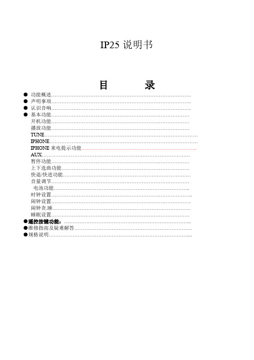
IP25说明书目录●功能概述……………………………………………………………………….●声明事项……………………………………………………………………….●认识音响……………………………………………………………………….●基本功能………………………………………………………………………开机功能………………………………………………………………………播放功能………………………………………………………………………TUNE………………………………………………………………………………IPHONE……………………………………………………………………………IPHONE来电提示功能…………………………………………………………..AUX……………………………………………………………………………暂停功能………………………………………………………………………上下选曲功能…………………………………………………………………快退/快进功能…………………………………………………………………音量调节………………………………………………………………………电池功能……………………………………………………………………..时钟设置………………………………………………………………………..闹钟设置……………………………………………………………………….闹钟贪.睡………………………………………………………………………睡眠设置………………………………………………………………………●遥控按键功能:………………………………………………………………...●维修指南及疑难解答……………………………………………………………●规格说明………………………………………………………………………....●介绍感谢尊贵的您选购我们的新一代多功能组合迷你音响!此款组合迷你音响,具有多种功能复合,本机完美的音质、及极高的可靠性和精巧的外观相得益彰,堪称大师级的作品,衷心的希望能给喜欢音乐的您带来数码时代的超凡享受。
PHOENIX CONTACT 5孔绿色插针5-pos版商品说明书

Extract from the onlinecatalogPCV 4/ 2-G-7,62Order No.: 1804687The figure shows a 5-pos. version of the producthttp://eshop.phoenixcontact.de/phoenix/treeViewClick.do?UID=1804687Header, Nominal current: 20 A, Nom. voltage: 400 V, Pitch: 7.62 mm, Number of positions: 2, Color: green, Assembly: Solderinghttp://Please note that the data givenhere has been taken from theonline catalog. For comprehensiveinformation and data, please referto the user documentation. TheGeneral Terms and Conditions ofUse apply to Internet downloads. Technical dataDimensions / positionsPitch7.62 mmDimension a7.62 mmNumber of positions2Pin dimensions 1 x 0,8 mmHole diameter 1.3 mmTechnical dataInsulating material group IRated surge voltage (III/3) 6 kVRated surge voltage (III/2) 6 kVRated surge voltage (II/2) 6 kVRated voltage (III/2)630 VRated voltage (II/2)630 VConnection in acc. with standard EN-VDENominal current I N20 ANominal voltage U N400 VMaximum load current20 AInsulating material PAInflammability class acc. to UL 94V0Certificates / ApprovalsCertification BV, CSA, CUL, DNV, GL, GOST, LR, RS, ULCSANominal voltage U N300 VNominal current I N20 ACULNominal voltage U N300 VNominal current I N35 AULNominal voltage U N300 VNominal current I N35 AAccessoriesItem Designation DescriptionAssembly1827570BF-PC 4Mounting flange, is snapped onto the left and right of the headers,for screw connection with PC 4/...-STF-7.62Marking1051993B-STIFT Marker pen, for manual labeling of unprinted Zack strips, smear-proof and waterproof, line thickness 0.5 mm0804549SK 7,62/3,8:FORTL.ZAHLEN Marker card, printed horizontally, self-adhesive, 10-section markerstrip, 12 identical decades marked 1-10, 11-20 etc. up to 91-99,sufficient for 120 terminal blocks0805153SK 7,62/3,8:SO Marker card, special printing, self-adhesive, labeled acc. tocustomer requirements, 12 identical marker strips per card, max.25-position labeling per strip, color: white0803906SK U/3,8 WH:UNBEDRUCKT Unprinted marker cards, DIN A4 format, pitch as desired, self-adhesive, with 40 stamped marker strips, 185 mm strip length, canbe labeled with the CMS system or manually with the M-PENPlug/Adapter1600027CP-HCC 4Coding profile, Color: redAdditional productsItem Designation DescriptionGeneral1848892PC 4 HV/ 2-ST-7,62Plug component, Nominal current: 20 A, Nom. voltage: 800 V,Pitch: 7.62 mm, Number of positions: 2, Connection type: Screwconnection, Color: green1882379PC 4 HV/ 2-STF-7,62Plug component, Nominal current: 20 A, Nom. voltage: 800 V,Pitch: 7.62 mm, Number of positions: 2, Connection type: Screwconnection, Color: green1804904PC 4/ 2-ST-7,62Plug component, Nominal current: 20 A, Nom. voltage: 400 V,Pitch: 7.62 mm, Number of positions: 2, Connection type: Screwconnection, Color: green1828249PC 4/ 2-STF-7,62Plug component, Nominal current: 20 A, Nom. voltage: 400 V,Pitch: 7.62 mm, Number of positions: 2, Connection type: Screwconnection, Color: green1840191PCC 4/ 2-ST-7,62Plug component, Nominal current: 20 A, Nom. voltage: 400 V,Pitch: 7.62 mm, Number of positions: 2, Connection type: Crimpconnection, Color: greenDiagrams/DrawingsDrilling plan/solder pad geometryDimensioned drawingAddressPHOENIX CONTACT Inc., USA586 Fulling Mill Road Middletown, PA 17057,USA Phone (800) 888-7388Fax (717) 944-1625© 2010 Phoenix Contact Technical modifications reserved;。
INFINEON IPP50R199CP 说明书
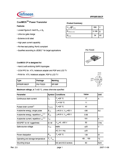
IPP50R199CPMaximum ratings, at T j =25 °C, unless otherwise specified ParameterSymbol Conditions Unit Continuous diode forward current I S ADiode pulse current2)I S,pulse 40Reverse diode d v /d t 4)d v /d t15V/nsParameter Symbol ConditionsUnitmin.typ.max.Thermal characteristicsThermal resistance, junction - case R thJC --0.9K/WR thJAleaded--62Soldering temperature,wavesoldering only allowed at leadsT sold 1.6 mm (0.063 in.) from case for 10 s--260°CElectrical characteristics, at T j =25 °C, unless otherwise specified Static characteristicsDrain-source breakdown voltage V (BR)DSS V GS =0 V, I D =250 µA 500--VGate threshold voltageV GS(th)V DS =V GS , I D =0.66 mA 2.533.5Zero gate voltage drain current I DSS V DS =500 V, V GS =0 V, T j =25 °C--1µAV DS =500 V, V GS =0 V, T j =150 °C-10-Gate-source leakage current I GSS V GS =20 V, V DS =0 V --100nA Drain-source on-state resistanceR DS(on)V GS =10 V, I D =9.9 A, T j =25 °C-0.180.199ΩV GS =10 V, I D =9.9 A, T j =150 °C-0.45-Gate resistanceR Gf =1 MHz, open drain-2.2-ΩValue T C =25 °C9.9Values Thermal resistance, junction - ambientIPP50R199CPParameterSymbol ConditionsUnitmin.typ.max.Dynamic characteristics Input capacitance C iss -1800-pFOutput capacitanceC oss-80-Effective output capacitance, energyrelated 5)C o(er)-75-Effective output capacitance, time related 6)C o(tr)-160-Turn-on delay time t d(on)-35-nsRise timet r -14-Turn-off delay time t d(off)-80-Fall timet f-10-Gate Charge Characteristics Gate to source charge Q gs -8-nCGate to drain charge Q gd -11-Gate charge total Q g -3445Gate plateau voltage V plateau-5.2-VReverse Diode Diode forward voltage V SD V GS =0 V, I F =9.9 A, T j =25 °C-0.9 1.2V Reverse recovery time t rr -340-ns Reverse recovery charge Q rr -4-µC Peak reverse recovery currentI rrm-24-A1)J-STD20 and JESD222)Pulse width t p limited by T j,max3)Repetitive avalanche causes additional power losses that can be calculated as P AV =E AR *f.6)C o(tr) is a fixed capacitance that gives the same charging time as C oss while V DS is rising from 0 to 80% V DSS.4)I SD ≤I D , d i /d t ≤200A/µs, V DClink =400V, V peak <V (BR)DSS , T j <T jmax , identical low and high side switchV R =400 V, I F =I S , d i F /d t =100 A/µs5)C o(er) is a fixed capacitance that gives the same stored energy as C oss while V DS is rising from 0 to 80% V DSS.Values V GS =0 V, V DS =100 V, f =1 MHzV DD =400 V,V GS =10 V, I D =9.9 A, R G =16.4 ΩV DD =400 V, I D =9.9 A, V GS =0 to 10 VV GS =0 V, V DS =0 V to 400 V1 Power dissipation5 Typ. output characteristics9 Typ. gate charge13 Typ. capacitancesIPP50R199CP Definition of diode switching characteristicsIPP50R199CP PG-TO220-3-1/TO220-3-21: OutlineIPP50R199CPPublished byInfineon Technologies AG81726 Munich, Germany© 2007 Infineon Technologies AGAll Rights Reserved.Legal DisclaimerThe information given in this document shall in no event be regarded as a guarantee ofconditions or characteristics. With respect to any examples or hints given herein, any typicalvalues stated herein and/or any information regarding the application of the device,Infineon Technologies hereby disclaims any and all warranties and liabilities of any kind,including without limitation, warranties of non-infringement of intellectual property rightsof any third party.InformationFor further information on technology, delivery terms and conditions and prices, pleasecontact the nearest Infineon Technologies Office().WarningsDue to technical requirements, components may contain dangerous substances. For informationon the types in question, please contact the nearest Infineon Technologies Office.Infineon Technologies components may be used in life-support devices or systems only withthe express written approval of Infineon Technologies, if a failure of such components canreasonably be expected to cause the failure of that life-support device or system or to affectthe safety or effectiveness of that device or system. Life support devices or systems areintended to be implanted in the human body or to support and/or maintain and sustainand/or protect human life. If they fail, it is reasonable to assume that the health of the useror other persons may be endangered.。
ip5306中文资料
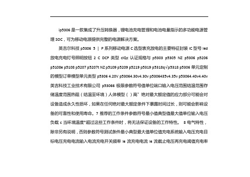
ip5306是一款集成了升压转换器,锂电池充电管理和电池电量指示的多功能电源管理SOC,可为移动电源提供完整的电源解决方案。
英吉尔科技p5306 5 | P系列移动电源C选型表充放电的主要特征封装IC型号led 放电充电灯号照明按钮2 C DCP类型cIQc认证规格与p5303 p5305 NZ p5306 p5206 p5108e p5108 p5207 p5207t NZ p5109 p5209 p5219 p5319 p5318q√p5318 p5306单元定制的模型订单模型单元类型p5306 4.20V p53064.30v4.30v p5306435v4.35v p53064.40v4.40v 英吉科技工业技术有限公司p53066极限参数符号值单位端口输入电压范围结温范围存储温度范围热阻(结温至环境)人体模型()高”绝对最大额定值的应力部分可能会对设备造成永久性损坏,如果在任何绝对最大额定条件下暴露时间过长,则可能会影响设备的可靠性和使用寿命。
7推荐的工作条件参数符号最小值典型值最大值单位输入电压负载c当环境温度*超过这些工作条件时,将无法保证设备的工作特性。
8电气特性,除非另有说明,否则参数符号测试条件最小典型最大值单位值充电系统输入电压充电目标电压充电电流输入电流充电开关频率le流充电电流le流截止电压再充电阈值充电率截止时间输入欠压保护升压英集科技工业技术p5306欠压保护迟滞升压系统电池电压开关操作电池输入电流输出电压输出电压输出电压纹波△V升压开关频率升压系统电源电流负载过电流检测时间输出电压持续低于负载短路检测时间输出电流持续大于控制系统的导通电阻电池输入等待电流照明驱动电流显示驱动电流负载自动检测时间负载电流持续减小s比短键唤醒时间更准时,热关断温度上升温度℃,热关断温度滞后△t℃英吉,而科技工业技术p5306 9灯显示模式D4 D3 D2 D1四灯D2 D1 D1灯蝙蝠1K L1两灯蝙蝠D2 D1扁平L1灯1K套,同时工业技术p5306■4灯模式放电能量()C≥75%50%≤C <开,开,开,关,25%≤C <3%≤C <开,关,闪烁,充电容量()完全打开,75%≤C,开,开,开,开,开,开,50%≤C,开,25%≤C,开,关,关,25 %≤C,打开,关闭,关闭,25%≤C <打开,关闭,关闭,25%≤C <打开,关闭,关闭,25%≤C <打开,关闭,关闭,25%≤C <打开,灭,灭,25%≤C <亮,灭,灭,25%≤C <亮,各灯的相应电池电量如下表所示。
IPB50R140CP中文资料

CoolMOSTM Power Transistor
Features • Lowest figure of merit RON x Qg • Ultra low gate charge • Extreme dv/dt rated • High peak current capability • Pb-free lead plating; RoHS compliant • Quailfied according to JEDEC1) for target applications
10-4
10-3
10-2
t p [s]
10-1
45
30
15
0 0
6V
5.5 V
5V 4.5 V
5
10
15
20
V DS [V]
Rev. 2.0
page 4
2007-11-20
元器件交易网
I D [A] R DS(on) [Ω]
5 Typ. output characteristics I D=f(V DS); T j=150 °C parameter: V GS
Type IPB50R140CP
Package PG-TO263
Marking 5R140P
Maximum ratings, at T j=25 °C, unless otherwise specified
Parameter
Symbol Conditions
Continuous drain current
6V
0.5
5V
0.4
4.5 V
0.3
0
0
5
10
15
20
ZJY51R5-2P-01;ZJY51R5-2PB-01;ZJY51R5-2PL-01;ZJY51R5-M4PA-01;ZJY51R5-4P-01;中文规格书,Datasheet资料

•All specifications are subject to change without notice.•Conformity to RoHS Directive: This means that, in conformity with EU Directive 2002/95/EC, lead, cadmium, mercury, hexavalent chromium, and specific Common Mode FiltersFor general signal line/power line ZJY seriesType:Issue date:ZJY51R5September 2011Common Mode FiltersFor General Signal Line / Power LineZJY Series ZJY51R5FEATURES• A common mode filter for distortion-free removal of noise from transmitted signals. Best common mode filter for transmission of high quality signals.•Best filter for countering the common mode noise resulting from data signal processing by PCs, phone equipment, etc.•Highly appropriate for IC board mounting due to DIP type struc-ture.•Due to a maximum current tolerance of 2A, can also be used to counter power line noise.APPLICATIONSPersonal computers, telephones, LANs, ISDNs, digital PBXs, elec-tronic games, CTVs, CD-ROM drives, 8mm video equipment, and other electronic devicesPACKAGING STYLE AND QUANTITIES (Tube style)RECOMMENDED SOLDERING CONDITIONRECOMMENDED FLOW TEMPERATURE PROFILE FOR LEAD-FREE SOLDERSHAPES AND DIMENSIONS TRANSFER MOLDPLASTIC CASE ZJY51R5-2P-01, -2PB-01, -2PL-01ZJY51R5-4P-01, -M4PA-01ZJY51R5-8PA-01Dimensions in mmCIRCUIT DIAGRAMSZJY51R5-2P-01, -2PB-01, -2PL-01ZJY51R5-4P-01, -M4PA-01ZJY51R5-8PA-01Conformity to RoHS DirectiveZJY51R5-2PB-0180 pieces ZJY51R5-2PL-0180 pieces ZJY51R5-4P-0140 pieces ZJY51R5-M4PA-0140 pieces ZJY51R5-8PA-0120 piecesPart No. A max. B max. C max. D max.E F±0.25G H I ZJY51R5-2P-01, -2PB-01, -2PL-01∗ 5.5 6.86 4.57 5.840.5 2.547.620.25 2.54ZJY51R5-4P-01, -M4PA-0110.5 6.86 4.57 5.840.5 2.547.620.25 2.54ZJY51R5-8PA-0123.57 4.6 6.30.52.547.620.252.54•Conformity to RoHS Directive: This means that, in conformity with EU Directive 2002/95/EC, lead, cadmium, mercury, hexavalent chromium, and specificELECTRICAL CHARACTERISTICS∗1 This type has improved low-range characteristics.∗2 This type is wrapped separately (for communication lines).TYPICAL ELECTRICAL CHARACTERISTICSIMPEDANCE CHARACTERISTICS (for 1 element)ZJY51R5-2P-01, -4P-01, -8PA-01ZJY51R5-2PB-01ZJY51R5-2PL-01ZJY51R5-M4PA-01MEASURING CIRCUITTYPICAL APPLICATIONAn application example showing how radiation noise is prevented when transmitter and receiver are connected via twisted pair cables.Part No.ZJY51R5-2P-01, -4P-01ZJY51R5-2PB-01∗1ZJY51R5-2PL-01∗2ZJY51R5-M4P A-01ZJY51R5-8P A-01Rated voltage Edc(V)5050505050Rated current (A)2220.50.5T est voltage Edc(V)[Between terminals for 5s]125125*********[Between terminals at DC.50V for 1min]100 min.100 min.100 min.100 min.100 min.DC resistance (Ω) [Each line]0.12 max.0.12 max.0.10 max.0.25 max.0.07 max.Operating temperature range (°C)–25 to +85–25 to +85–25 to +85–25 to +85–25 to +85Storage temperature range(After mount)(°C)–25 to +85–25 to +85–25 to +85–25 to +85–25 to +85Impedance (Ω) [+5 to +35°C][20 to 300MHz][6 to 20MHz][20 to 100MHz][20 to 300MHz][20 to 300MHz]分销商库存信息:TDKZJY51R5-2P-01ZJY51R5-2PB-01ZJY51R5-2PL-01 ZJY51R5-M4PA-01ZJY51R5-4P-01。
PQ05RF1中文资料

s Outline Dimensions
10.2MAX 4.5±0.2
(Unit : mm)
2.8±0.2
7.4±0.2
29.1MAX
PQ05RF1
4-1.4
+0.3 -0
13.5MIN
4-0.6
+0.2 -0.1
s Model Line-ups
Output voltage Output voltage precision:±5% Output voltage precision:±2.5%
2.0
Fig.5 Output Voltage Minute Adjustment Characteristics (PQ05RF1V)
6.0 R1=390Ω R1=1kΩ
Output voltage VO (V)
Fig.6 Output Voltage Minute Adjustment Characteristics (PQ09RF1V)
Symbol VIN VC IO PD1 PD2 Tj Topr Tstg Tsol
Rating 35 35 1 1.5 15 150 -20 to +80 -40 to +150 260 (For 10s)
Unit V V A W W ˚C ˚C ˚C ˚C
*1 *2
All are open except GND and applicable terminals. Overheat protection may operate at 125=<Tj=<150˚C
15
PD2
80 60 40
10
5 PD1
20 0
0 50 100 150 Ambient temperature Ta (˚C) Note) Oblique line portion:Overheat protection may operate in this area.
EC5525NPAP-1 商品说明书
EC5525PPAP-1EC 55 25 NPAPSpecifications are subject to change without notice (25.06.99)1Type SelectionProduct DescriptionProximity Sensors Capacitive Flat pack Polycarbonate Housing Type EC 5525, DCCapacitive proximity switches with sensing distance 16 mm flush mounted and sensing distance 25 mm non-flush mounted by adjustment. 4-wire DC output with both make (N O) and break (N C)switching. Flat pack housing,size (WxHxD) 35 x 55 x 15 mm made in polycarbonate. Easy mounting with only two M4screws. Ideal for use in materi-al handling and plastic ma-chinery applications.Housing Rated Ordering no.Ordering no.Ordering no.Ordering no.dimensions operating NPN/cableNPN/plugPNP/cablePNP/plugW x H x D dist. (S n )1)Make & break swit.Make & break swit.Make & break swit.Make & break swit.Flush/non-flush 35 x 55 x 1516/25 mmEC 5525 NPAPEC 5525 NPAP-1EC 5525 PPAPEC 5525 PPAP-11)Object: Grounded steel plateT R I P L E S H I E L D ™• Featuring TRIPLESHIELD ™ sensor protection•Adjustable sensing distance 4-25 mm •Rated operational voltage: 10-40 VDC •Output: DC 200 mA, NPN or PNP•Make and break switching function, LED indication •Capacitive, Inductive and Photoelectric flat pack series in PC housing, IP 67•High noise immunity•Universal flush and non-flush mountable •Plug and cable versions2Specifications are subject to change without notice (25.06.99)EC 5525object distanceand industrial (noise) interference.Because of this, Carlo Gavazzi offers as standard features in allInstallation HintsCapacitive sensors have the unique ability to detect almost all materials, either in liquid or solid form. Capacitive sensors can detect metallic as well as non-metallic objects, however , their traditional use is for non-metallic materials such as:•Plastic IndustryResins, regrinds or moulded products.•Chemical IndustryCleansers, fertilisers, liquid soaps, corrosives and petro-chemicals.•Wood IndustrySaw dust, paper products,door and windowframes.•Ceramic & Glass Industry Raw material, clay or finished products, bottles.•Packaging Industry Packa-ge inspection for level or con-tents, dry goods, fruits and vegetables, dairy products.Materials are detected due to their dielectric constant. The big-ger the size of an object, the hig-her the density of material, the better or easier it is to detect the object. Nominal sensing distance for a capacitive sensor is referen-ced to a grounded metal plate (ST37). For additional information regarding dielectric ratings of materials please refer to T echnical Information.Delivery Contents•Capacitive switch: EC55.. PAP(-1)•Screw driver•Packaging:Cardboard box •Installation & Adjustment Guide• Plugs CON.1A.. serieFor further information refer to “Accessories”.EC5525PPAP-1EC 55 25 NPAP。
WD-9915P(共用版)使用手册说明书

使用說明書WD-9915P為充分發揮本機功能,在您使用前請詳細閱讀本說明書,並妥善保存,作為日後參考V1.01208◎當發生異常或有燒焦味時,應立即拔除電源或電池,若在異常狀態下繼續使用,易造成火災之發生。
◎請速與本公司服務專線聯絡或就近經銷商洽詢。
MP3數位錄音筆目錄(一)本機特點 (2)(二)免責聲明 (2)(三)安全注意事項 (3)(四)外型及各部位名稱 (4)(五)基本操作 (5)充電 (5)開機/關機 (5)錄音操作 (5)暫停錄音 (5)音樂及錄音播放 (6)上/下曲 (6)音量調整 (6)耳機的使用 (6)(六)與電腦連結 (7)連結電腦 (7)(七)疑難排解 (8)(八)故障排除 (9)(九)規格 (9)請詳細閱讀本說明書,讓您輕鬆操作,使用 EASY! 11.單鍵錄音功能2.鋅合金外殼,高強度可有效保護機器。
3.內置高靈敏度麥克風。
4.內建高品質喇叭。
5.耳機插座。
6.電池電力指示,自動省電關機功能。
7.錄音指示燈功能,錄音一目了然。
免責聲明●聲明:此產品為電子數位機器,如有電源不穩(連接電腦或電池)的現象及操作不當,可能會導致資料遺失。
在此強烈建議您將重要資料備份。
本公司對於任何資料遺失所造成的損失或賠償恕難負責。
本手冊業經仔細檢查及校對,但仍不排除文字拼寫及技術錯誤之可能,若因錯誤導致與實機不符時,以實機為準,此種錯誤或疏漏不能當呈堂的依據,其將於新版予以修正。
本手冊之全部內容,本公司享有隨時修改之權力,且不另行通知。
2在使用本機之前,應仔細閱讀下列事項及使用說明,閱後並請妥為收存,以備將來參考:1.本機請勿置於雨中、濕氣中或避免陽光直射及遠離其他會產生熱能的裝置。
2.在本機和電腦連接進行通訊時,不要隨意扭動USB連線,以免資料中斷影響正常 操作,而導致資料存取毀損。
3.在解除本機與電腦的連接前,先點擊電腦桌面右下角的USB圖示安全移除,再拔 出USB連接線,這樣會減少電腦和本機出現錯誤。
施耐德电涌保护器选型方案

标注方式
iPRC
iPRI
产品型号
产品型号
产品参数
产品名称
Un (V)
Uc (V) Up (kV) 波形 (µs)
iPRC型
iPRC
130 VAC
<130 VAC
300V
180 VDC
8/20
iPRI型
37 VAC
48 VDC
70V 8/20
53 VDC
iPRI
Imax (kA)
18
In (kA)
极数 工作状态 远程指示 指示窗口 触点
36
25
iSCB2 20N2
+
iPRU 10
15
iSCB2 20N1
+
iPRU 10
iSCB2 65H2
+
iPRU 40(r)
iSCB2 65H2
+
iPRU 65r
iSCB2 20N2
+
iPRU 20(r)
iSCB2 20N1
+
iPRU 20(r)
iSCB2 65H1
+
iPRU 40(r)
iSCB2 65H1
+
iPRU 65r
iSCB2 120L1
+
iPRU 80r
iSCB2 120L1
+
iPRU 120r
10 kA
20 kA
40 kA
65 kA
80 kA
120 kA
Imax
注意: ● 此选型表中电涌保护器与后备保护装置的配合关系经过全面的试验验证。 ● 电涌保护器每极都必须设置保护。例如:3P+N 的电涌保护器必须用4P的iSCB。
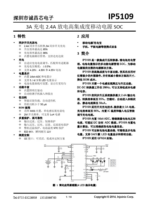
IP5109 datasheet v1.0
按键
KEY
图 3
KEY 按键
按键连接方式如图 2 所示, 可识别长按键和短按键操作。 按键持续时间长于 30ms,但小于 2s, 即为短按动作,短按会打开电量显示灯和升压输出。 按键持续时间长于 2s, 即为长按动作, 长按会开启或者关闭照明 LED。 小于 30ms 的按键动作不会有任何响应。 在 1s 内连续两次短按键,会关闭升压输出、电量显示和照明 LED。
无 100% 80%
无 无 100%
电池内阻设定
IP5109 可以通过 RSET 引脚设定电池内阻,从而调节 LED 电量显示的均匀特性。RSET 电阻大小和 设定的电池内阻如下表所示。 RSET 端电阻 Kohm 184 174 164 154 144 134 124 114 104 94 84 74 64 54 44 34 对应电池设定内阻(mOhm) 165 155 145 135 125 110 100 90 80 70 60 40 30 20 10 0
IP5109
12 4.5 200 Hour V mV
3.0 3 100 5.0 50 2.4 30 150
4.4
V mA uA V mV A ms
200
us
1.5 50 30
MHz mΩ mΩ V uA mA mA
VREG ISTB ILDO Ilight IL1 IL2 IL3 IL4 TloadD TOnDebounce TKeylight TOTP ΔTOTP
*超出这些工作条件,器件工作特性不能保证。
8 电气特性
除特别说明,TA=25℃,L=1uH 参数 充电系统 输入电压 输入工作电流 输入静态电流 充电目标电压 充电电流 涓流充电电流 涓流截止电压 再充电阈值 IVIN VTRGT ICHRG ITRKL VTRKL VRCH VIN=5v,BAT=2.7v 100 3 4.1 VIN VIN=5V,fs=1.5MHz VIN=5V,Device not switching 100 4.2 3 4.5 5 5.5 2 V mA uA V A mA V V 符号 测试条件 最小 值 典型 值 最大 值 单位
IP6505降压快充芯片datasheet

支持 BC1.2、Apple、三星协议 支持高通 QC2.0 和 QC3.0(认证编号:
4788120153-2) 支持 MTK PE1.1/PE2.0 支持华为快充协议 FCP 支持华为快充协议 SCP 支持三星快充协议 AFC 支持展讯快充协议 SFCP
多重保护、高可靠性
Idc(A)Max.
Saturation Current
图 4 输出应用原理图
7 / 10
TEL:18319027317
IP6505
11 BOM 表
序号 元件名称
型号&规格
单位 用量
位置
1 IC
IP6505
PCS
2 贴片电阻
0603 3.3K 5%
PCS
3 贴片电阻
0603 75K 1%
PCS
TC-220M-4. 22uH+/-20%,电流 4.5A
4 5A-CS1371 DCR<12mohm
6 / 10
TEL:18319027317
IP6505
10 典型应用原理图
IP6505 外围只需要电感、电容、电阻, 即可实现完整功能的车充方案
VOUT R2 3.3K
VOUT
22uH L1
SW 1
DM
DP
C5 C4
SW
C3
2
R4
10uF
220uF
2R 0.1uFBST
3
C6 1nF FS
R3 75k
开关频率设定
IP6505 可以通过 FS 来设定开关频率大小。DCDC 开关频率和电阻的对应关系如下表.
FS 外接电阻(ohm) 47K
75k
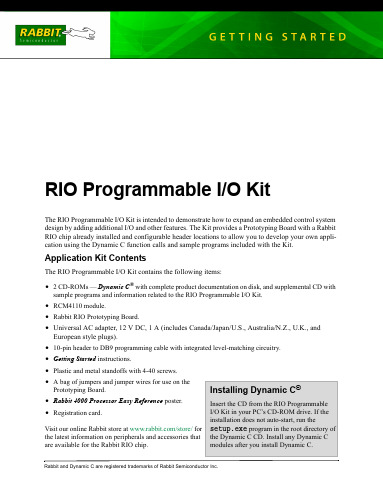
瑞兔(Rabbit)半导体公司注册商标的RIO可编程I O套件说明书
Rabbit and Dynamic C are registered trademarks of Rabbit Semiconductor Inc.RIO Programmable I/O KitThe RIO Programmable I/O Kit is intended to demonstrate how to expand an embedded control system design by adding additional I/O and other features. The Kit provides a Prototyping Board with a Rabbit RIO chip already installed and configurable header locations to allow you to develop your own appli-cation using the Dynamic C function calls and sample programs included with the Kit.Application Kit ContentsThe RIO Programmable I/O Kit contains the following items:• 2 CD-ROMs — Dynamic C ® with complete product documentation on disk, and supplemental CD withsample programs and information related to the RIO Programmable I/O Kit.•RCM4110 module.•Rabbit RIO Prototyping Board.•Universal AC adapter, 12 V DC, 1 A (includes Canada/Japan/U.S., Australia/N.Z., U.K., andEuropean style plugs).•10-pin header to DB9 programming cable with integrated level-matching circuitry.•Getting Started instructions.•Plastic and metal standoffs with 4-40 screws.•A bag of jumpers and jumper wires for use on the Prototyping Board.•Rabbit 4000 Processor Easy Reference poster.•Registration card.Visit our online Rabbit store at /store/ for the latest information on peripherals and accessories that are available for the Rabbit RIO chip.Installing Dynamic C ®Insert the CD from the RIO Programmable I/O Kit in your PC’s CD-ROM drive. If the installation does not auto-start, run thesetup.exe program in the root directory of the Dynamic C CD. Install any Dynamic Cmodules after you install Dynamic C .Hardware Connections1. Prepare the Prototyping Board for DevelopmentSnap in four of the plastic standoffs supplied in the bag of accessory parts from the RIO Programmable I/O Kit in the holes at the corners as shown.2. Attach Module to Prototyping BoardTurn the RCM4110 module so that the mounting holes of the RCM4110 line up with the corresponding holeson the Prototyping Board. Insert the metal standoffs as shown in Figure 2, secure them from the bottom of the Prototyping Board using the 4-40 × 3/16 screws, then insert the module’s header J3 on the bottom side into header socket RCM1 on the Prototyping Board.Figure 2. Install the RCM4110 Module on the Prototyping BoardNOTE:It is important that you line up the pins on header J3 of the RCM4110 module exactly with socket RCM1 on the Prototyping Board. The header pins may become bent or damaged if the pin alignment is offset, and the module will not work. Permanent electrical damage to the module may also result if a misaligned module is powered up.Press the module’s pins gently into the Prototyping Board header socket—press down in the area above the header pins. For additional integrity, you may secure the RCM4110 to the standoffs from the top using the remaining two 4-40 × 3/16 screws.3. Set JumpersJumpers were placed at the factory on Prototyping Board headers J2, J7, J8, J9, and J15 as shown in Figure 3 to set up the Prototyping Board for the SPI serial mode used with the sample programs. Application Note AN415, RIO Programmable I/O Kit , describes other configuration options.4. Connect Programming CableThe programming cable connects the RCM4110 to the PC running Dynamic C to download programs and to monitor the RCM4110 module during debugging.Connect the 10-pin connector of the programming cable labeled PROG to header J1 on the RCM4110 as shown in Figure 3. Be sure to orient the marked (usually red) edge of the cable towards pin 1 of the connector. (Do not use the DIAG connector, which is used for a normal serial connection to Serial Port A.)Figure 1. Insert Plastic StandoffsFigure 3. Prototyping Board and Programming Cable SetupNOTE:Be sure to use the programming cable (part number 101-0542) supplied with the RIOProgrammable I/O Kit—the programming cable has blue shrink wrap around the RS-232 con-verter section located in the middle of the cable. Programming cables with red or clear shrinkwrap from other Rabbit Semiconductor kits are not designed to work with RCM4110 modules. Connect the other end of the programming cable to a COM port on your PC.NOTE:Some PCs now come equipped only with a USB port. It may be possible to use an RS-232/USB converter (Part No. 540-0070) with the programming cable supplied with the RIO Pro-grammable I/O Kit. Note that not all RS-232/USB converters work with Dynamic C.5. Connect PowerOnce all the other connections have been made, you can connect power to the Prototyping Board. First, prepare the AC adapter for the country where it will be used by selecting the appropriate plug. The RIO Programmable I/O Kit presently includes Canada/Japan/U.S., Australia/N.Z., U.K., and European style plugs. Snap in the top of the plug assembly into the slot at the top of the AC adapter as shown in Figure3, then press down on the plug until it clicks into place.Connect the AC adapter to 3-pin header J1 on the Prototyping Board as shown in Figure3 above. The connector may be attached either way as long as it is not offset to one side—the center pin of J1 is always connected to the positive terminal, and either edge pin is ground.Plug in the AC adapter. The power LED on the Prototyping Board above the power connector at J1 should light up. The RCM4110 and the Prototyping Board are now ready to be used.NOTE:If you need to reset the RCM4110, disconnect, then reconnect the power supply.Starting Dynamic COnce the RCM4110 is connected as described in the preceding pages, start Dynamic C by double-clicking on the Dynamic C icon on your desktop or in your Start menu. Dynamic C uses the serial port specified during installation.If you are using a USB port to connect your computer to the RCM4110, choose Options > Project Options and check “Use USB to Serial Converter” in “Serial Options.” Click OK to save the settings. Run a Sample ProgramUse the File menu to open the sample program ROTATELED.C in the Dynamic C SAMPLES\RIO folder. Press function key F9 to compile and run the program.The four LEDs on the Prototyping Board will flash on and off in a rotating sequence, and the Dynamic C STDIO window will open on your PC to display the status of the Rabbit RIO chip’s Channel 1.This sample program uses Channel 1 with the Rabbit RIO chip operating in the SPI clocked serial communi-cation mode. The Rabbit RIO Chip User's Manual describes the communication modes in more detail. Where Do I Go From Here?If the sample program ran fine, you are now ready to go on to other sample programs and to develop your own applications. Application Note AN415, RIO Programmable I/O Kit, discusses how to use the Prototyp-ing Board and explains the sample programs and Rabbit RIO function calls. The source code for the sample programs is provided to allow you to modify them for your own use. The RCM4100 User's Manual on the Dynamic C CD also provides complete hardware reference information and describes the software function calls for the RCM4110 RabbitCore module, and the Rabbit RIO User's Manual provides complete reference information for the Rabbit RIO chip.TroubleshootingIf Dynamic C cannot find the target system (error message "No Rabbit Processor Detected."):•Check that the RCM4110 is powered correctly — the red power LED on the Prototyping Board should be lit when the RCM4110 is mounted on the Prototyping Board and the AC adapter is plugged in.•Check both ends of the programming cable to ensure that they are firmly plugged into the PC and the PROG connector, not the DIAG connector, is plugged in to the programming port on the RCM4110.•Ensure that the RCM4110 module is firmly and correctly installed in its socket on the Prototyping Board. If there are no faults with the hardware, select a different COM port within Dynamic C. On your computer, open Control Panel > System > Hardware > Device Manager > Ports and look at the list of available COM ports. In Dynamic C, select Options > Project Options, then select one of the available COM ports on the “Communications” tab, then click OK. Press <Ctrl-Y> to force Dynamic C to recompile the BIOS. If Dynamic C still reports it is unable to locate the target system, repeat the above steps for another available COM port. You should receive a Bios compiled successfully message once this step is com-pleted successfully.If a program compiles and loads, but then loses target communication before you can begin debugging, it is possible that your PC cannot handle the default debugging baud rate. Try lowering the debugging baud rate.•Locate the Serial Options dialog in the Dynamic C Options > Project Options > Communica-tions menu. Choose a lower debug baud rate.If there are any other problems:•Use the Dynamic C Help menu to get further assistance with Dynamic C.•Check the Rabbit Semiconductor Technical Bulletin Board at /support/bb/.•Use the Technical Support e-mail form at /support/.NOTE:If you purchased your RIO Programmable I/O Kit through a distributor or through a RabbitSemiconductor partner, contact the distributor or partner first for technical support.020–0124•070715–C。
protel 99 英汉对照

Protel 99各元器件名字中英文对照表2009-04-13 13:33:51| 分类:ARM嵌入式学习| 标签:|举报|字号大中小订阅1. 标准电阻:RES1、RES2;封装:AXIAL-0.3到AXIAL-1.0两端口可变电阻:RES3、RES4;封装:AXIAL-0.3到AXIAL-1.0 三端口可变电阻:RESISTOR TAPPED,POT1,POT2;封装:VR1-VR52.电容:CAP(无极性电容)、ELECTRO1或ELECTRO2(极性电容)、可变电容CAPVAR封装:无极性电容为RAD-0.1到RAD-0.4,有极性电容为RB.2/.4到RB.5/1.0.3.二极管:DIODE(普通二极管)、DIODE SCHOTTKY(肖特基二极管)、DUIDE TUNNEL(隧道二极管)DIODE VARCTOR(变容二极管)ZENER1~3(稳压二极管)封装:DIODE0.4和DIODE 0.7;(上面已经说了,注意做PCB时别忘了将封装DIODE的端口改为A、K)4.三极管:NPN,NPN1和PNP,PNP1;引脚封装:TO18、TO92A(普通三极管)TO220H(大功率三极管)TO3(大功率达林顿管)以上的封装为三角形结构。
T0-226为直线形,我们常用的9013、9014管脚排列是直线型的,所以一般三极管都采用TO-126啦!5、效应管:JFETN(N沟道结型场效应管),JFETP(P沟道结型场效应管)MOSFETN(N沟道增强型管)MOSFETP(P沟道增强型管)引脚封装形式与三极管同。
6、电感:INDUCTOR、INDUCTOR1、INDUCTOR2(普通电感),INDUCTORVAR、INDUCTOR3、INDUCTOR4(可变电感)8.整流桥原理图中常用的名称为BRIDGE1和BRIDGE2,引脚封装形式为D系列,如D-44,D-37,D-46等。
9.单排多针插座原理图中常用的名称为CON系列,从CON1到CON60,引脚封装形式为SIP系列,从SIP-2到SIP-20。
爱迪生187369型号RCCB电路保护设备说明书

Eaton 187369Eaton Moeller series xEffect - FRCmM Type F RCCB. Residual current circuit breaker (RCCB), 80A, 2p, 30mA, type G/FGeneral specificationsEaton Moeller series xEffect - FRCmM Type F RCCB187369401508182427480 mm 76 mm 35 mm 0.202 kg RoHS conformIEC/EN 62423 EN45545-2 IEC 61373 IEC/EN 61008FRCMM-80/2/003-G/FProduct NameCatalog Number EANProduct Length/Depth Product Height Product Width Product Weight Compliances Certifications Model CodeTwo-pole10 ms delayed80 A10 kA with back-up fuse 30 mAPulse-current sensitive3 kA (8/20 μs) surge-proof 240 V AC240 V440 V4 kV0.03 A0.03 A50 Hz / 60 Hz80 A (max. admissible back-up fuse)Other800 A80 A gG/gL10 kA3 kA184 V AC - 250 V AC2Frequency mix (10 Hz, 50 Hz, 1000 Hz) enhanced sensitivity 4000 operationsApplicationNumber of polesTripping timeAmperage RatingRated short-circuit strength Fault current rating Sensitivity typeImpulse withstand current Type Voltage rating (IEC/EN 60947-2)Rated operational voltage (Ue) - maxRated insulation voltage (Ui)Rated impulse withstand voltage (Uimp) Rated fault current - minRated fault current - maxFrequency ratingShort-circuit ratingLeakage current typeRated residual making and breaking capacity Admissible back-up fuse overload - max Rated short-time withstand current (Icw) Surge current capacityTest circuit rangePollution degreeRadiation resistanceLifespan, electricalSwitchgear for industrial and advanced commercial applicationsxEffect - Switchgear for industrial and advanced commercial applicationsCurrent test marks as per inscriptionMaximum operating temperature is 75 °C: Starting at 40 °C, the max. permissible continuous current decreases by 1.2% for every 1 °C45 mm235 mm (2 SU)70.5 mmQuick attachment with 2 latch positions for DIN-rail IEC/EN 60715DIN railAs requiredIP20IP20, IP40 with suitable enclosureWhite / blueTwin-purpose terminals1.5 mm² - 35 mm²1.5 mm²35 mm²16 mm² (2x)1.5 mm²16 mm²M5 (with cross-recessed screw as defined in EN ISO 4757-Z2, PZ2)80 A6.8 W13.6 W0 W0 W-25 °C40 °CMeets the product standard's requirements.Meets the product standard's requirements.Meets the product standard's requirements.Meets the product standard's requirements.Meets the product standard's requirements.Does not apply, since the entire switchgear needs to be evaluated.Does not apply, since the entire switchgear needs to be evaluated.FrameWidth in number of modular spacingsBuilt-in width (number of units)Built-in depthMounting MethodMounting positionDegree of protectionStatus indicationTerminals (top and bottom)Terminal capacity (solid wire)Connectable conductor cross section (solid-core) - min Connectable conductor cross section (solid-core) - max Terminal capacity (stranded cable)Connectable conductor cross section (multi-wired) - min Connectable conductor cross section (multi-wired) - max Terminal capacity (cable)Rated operational current for specified heat dissipation (In) Heat dissipation per pole, current-dependentEquipment heat dissipation, current-dependentStatic heat dissipation, non-current-dependentHeat dissipation capacityAmbient operating temperature - minAmbient operating temperature - max10.2.2 Corrosion resistance10.2.3.1 Verification of thermal stability of enclosures10.2.3.2 Verification of resistance of insulating materials to normal heat10.2.3.3 Resist. of insul. mat. to abnormal heat/fire by internal elect. effects10.2.4 Resistance to ultra-violet (UV) radiation10.2.5 Lifting10.2.6 Mechanical impact10.2.7 InscriptionsFinger and hand touch safe, DGUV VS3, EN 502742 Nm - 2.4 NmRed / green0.8 mm - 2 mm20000 operations-35 °C60 °C25-55 °C / 90-95% relative humidity according to IEC 60068-2Meets the product standard's requirements.Does not apply, since the entire switchgear needs to be evaluated.Meets the product standard's requirements.Does not apply, since the entire switchgear needs to be evaluated.Does not apply, since the entire switchgear needs to be evaluated.Is the panel builder's responsibility.Is the panel builder's responsibility.Is the panel builder's responsibility.Is the panel builder's responsibility.Is the panel builder's responsibility.The panel builder is responsible for the temperature rise calculation. Eaton will provide heat dissipation data for the devices.Is the panel builder's responsibility. The specifications for the switchgear must be observed.Is the panel builder's responsibility. The specifications for the switchgear must be observed.The device meets the requirements, provided the information in the instruction leaflet (IL) is observed.Terminal protectionTightening torqueContact position indicator colorBusbar material thicknessLifespan, mechanicalPermitted storage and transport temperature - min Permitted storage and transport temperature - max Climatic proofing 10.3 Degree of protection of assemblies10.4 Clearances and creepage distances10.5 Protection against electric shock10.6 Incorporation of switching devices and components 10.7 Internal electrical circuits and connections10.8 Connections for external conductors10.9.2 Power-frequency electric strength10.9.3 Impulse withstand voltage10.9.4 Testing of enclosures made of insulating material 10.10 Temperature rise10.11 Short-circuit rating10.12 Electromagnetic compatibility10.13 Mechanical functionFeatures Application notesEaton Corporation plc Eaton House30 Pembroke Road Dublin 4, Ireland © 2023 Eaton. All rights reserved. Eaton is a registered trademark.All other trademarks areproperty of their respectiveowners./socialmediaResidual current circuit breaker Additional equipment possibleInterlocking deviceShort-time delayed trippingType G/F (�VE E 8601) Residual current circuit breakers FRCmM eaton-rcd-application-guide-br019003en-en-us.pdfeaton-pdd-railrolling-stock-brochure-br011002en-en-us.pdfeaton-xeffect-frcmm-rccb-catalog-ca003018en-en-us.pdfDA-DC-03_FRCmeaton-circuit-breaker-xeffect-frcmm-na-rccb-dimensions.eps Mas_frcmmDA-CE-ETN.FRCMM-80_2_003-G_Featon-187365-3d-model.stpeaton-187365-drawing.dwgeaton-xeffect-frcmm-rccb-wiring-diagram.jpgFitted with: Functions Special featuresUsed with Brochures Catalogues Certification reports DrawingseCAD model mCAD model Wiring diagramsFRCmMResidual current circuit breakersType G/F (ÖVE E 8601)。
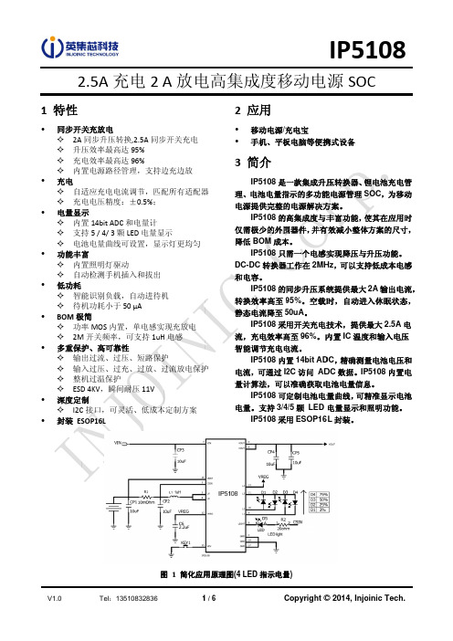
IP5109,IP5108,IP5206,IP5105 移动电源5合一芯片介绍
1 特性
同步开关 关充放电 2A 同步升压转 转换,2.5A 同步 步开关充电 升压 压效率最高达 达 95% 充电效率最高达 达 96% 内置 置电源路径管 管理,支持边 边充边放 充电 自适 适应充电电流 流调节,匹配 配所有适配器 器 充电电压精度: :±0.5%; 电量显示 示 内置 置 14bit ADC C 和电量计 支持 持 5 / 4/ 3 颗 LED 电量显 显示 电池 池电量曲线可 可设置,显示 示灯更均匀 功能丰富 富 内置 置照明灯驱动 动 自动 动检测手机插 插入和拔出 低功耗 智能 能识别负载, ,自动进待机 机 待机 机功耗小于 50 µA BOM 极 极简 功率 率 MOS 内置 置,单电感实 实现充放电 2M M 开关频率,可支持 1uH H 电感 多重保护 护、高可靠性 性 输出过流、过压 压、短路保护 护 输入 入过压、过充 充、过放、过 过流放电保护 护 整机 机过温保护 ESD D 4KV,瞬间 间耐压 11V 深度定制 制 I2C C 接口,可灵 灵活、低成本 本定制方案 封装 ES SOP16L
图 2 简化应用 用原理图(4 LED L 指示电量 量)
V1.0
Tel:13 3510832836
2/6
Copyright C © 2014, Injo oinic Tech.
1 特性
同步开关 关充放电 1A 同步升压转 转换,1.2A 同步 步开关充电 升压 压效率最高达 达 91% 充电效率最高达 达 93% 内置 置电源路径管 管理,支持边 边充边放 充电 自适 适应充电电流 流调节,匹配 配所有适配器 器 充电电压精度: :±0.5% 支持 持 4.2/4.3/4. .35v 电池 电量显示 示 支持 持 4/ 3 颗 LE ED 电量显示 示 功能丰富 富 内置 置照明灯驱动 动 自动 动检测手机插 插入和拔出 低功耗 智能 能识别负载, ,自动进待机 机 待机 机功耗小于 50 µA BOM 极 极简 功率 率 MOS 内置 置,单电感实 实现充放电 1.2 2M 开关频率 率,可支持 1u uH 电感 多重保护 护、高可靠性 性 输出过流、过压 压、短路保护 护 输入 入过压、过充 充、过放、过 过流放电保护 护 整机 机过温保护 ESD D 4KV,瞬间 间耐压 11V 深度定制 制 I2C C 接口,可灵 灵活、低成本 本定制方案
RXB50规格说明书

规格说明书RXB50 ASK超外差无线接收模块版本1.0深圳市晶美润科技有限公司深圳市晶美润科技有限公司V1.0目录1.概述.............................................................................................32.产品特性.....................................................................................33.产品脚位说明............................................................................44.电气参数.....................................................................................55.模块外形尺寸标注图................................................................66.模块名称解释............................................................................77.修改记录. (7)深圳市晶美润科技有限公司V1.01.概述RXB50超外差无线接收模块,采用法国品牌射频无线数据传送接收芯片,是一款性价比较高的ISM 频段的接收模块。
具有较高的接收灵敏度、体积小、低廉的价格,使得一些小体積的可以产品摆脱因为空間原因,提高了无线产品的稳定性及可靠性,改善了产品的品质与形象加强了产品竞争力。
无需外加任何电路即可以做到无线信号输入到数据信号输出。
用户只需要外加简单的数据解码电路,即可轻易实现无线产品的开发。
2.产品特性(1)接收灵敏度达到-110dBm;(2)工作频率:315MHz;433.92MHz;(特殊频率可以根据客户要求定做)(3)电源电压输入范围:3.6V-5.5V;(4)低电源功耗,5.0V @433.92MHz, 6.8mA;5.0V @315MHz,4.8mA;持续数据传输速率至2.4K 曼砌斯特編碼(5)良好的选择性和杂散辐射抑制能力,鏡頻抑制可以達到20dB深圳市晶美润科技有限公司V1.0(6)良好的本振辐射抑制能力,可多个接收模块一起工作(即单发多收)且不会互相干扰,一起使用不影响接收距离。
- 1、下载文档前请自行甄别文档内容的完整性,平台不提供额外的编辑、内容补充、找答案等附加服务。
- 2、"仅部分预览"的文档,不可在线预览部分如存在完整性等问题,可反馈申请退款(可完整预览的文档不适用该条件!)。
- 3、如文档侵犯您的权益,请联系客服反馈,我们会尽快为您处理(人工客服工作时间:9:00-18:30)。
UnitIPB50R199CPMaximum ratings, at T j =25 °C, unless otherwise specified ParameterSymbol Conditions Unit Continuous diode forward current I S ADiode pulse current 2)I S,pulse 40Reverse diode d v /d t 4)d v /d t15V/ns Parameter Symbol ConditionsUnitmin.typ.max.Thermal characteristicsThermal resistance, junction - caseR thJC --0.9K/WR thJASMD version, device on PCB, minimal footprint--62SMD version, device on PCB, 6 cm 2cooling area 5)-35-Soldering temperature, wave & reflowsoldering allowedT soldreflow MSL1--260°CElectrical characteristics, at T j =25 °C, unless otherwise specified Static characteristicsDrain-source breakdown voltage V (BR)DSS V GS =0 V, I D =250 µA 500--VGate threshold voltageV GS(th)V DS =V GS , I D =0.66 mA 2.533.5Zero gate voltage drain current I DSS V DS =500 V, V GS =0 V, T j =25 °C--1µAV DS =500 V, V GS =0 V, T j =150 °C-10-Gate-source leakage current I GSS V GS =20 V, V DS =0 V --100nA Drain-source on-state resistanceR DS(on)V GS =10 V, I D =9.9 A, T j =25 °C-0.180.199ΩV GS =10 V, I D =9.9 A, T j =150 °C-0.45-Gate resistanceR Gf =1 MHz, open drain-2.2-ΩValue T C =25 °C9.9Values Thermal resistance, junction - ambientIPB50R199CPParameterSymbol ConditionsUnitmin.typ.max.Dynamic characteristics Input capacitance C iss -1800-pFOutput capacitanceC oss-80-Effective output capacitance, energyrelated6)C o(er)-75-Effective output capacitance, time related7)C o(tr)-160-Turn-on delay time t d(on)-35-nsRise timet r -14-Turn-off delay time t d(off)-80-Fall timet f-10-Gate Charge Characteristics Gate to source charge Q gs -8-nCGate to drain charge Q gd -11-Gate charge total Q g -3445Gate plateau voltage V plateau-5.2-VReverse Diode Diode forward voltage V SD V GS =0 V, I F =9.9 A, T j =25 °C-0.9 1.2V Reverse recovery time t rr -340-ns Reverse recovery charge Q rr -4-µC Peak reverse recovery currentI rrm-24-A1) J-STD20 and JESD222) Pulse width t p limited by T j,max3) Repetitive avalanche causes additional power losses that can be calculated as P AV =E AR *f.7)C o(tr) is a fixed capacitance that gives the same charging time as C oss while V DS is rising from 0 to 80% V DSS.6)C o(er) is a fixed capacitance that gives the same stored energy as C oss while V DS is rising from 0 to 80% V DSS.4) I SD ≤I D , d i /d t ≤200A/µs, V DClink =400V, V peak <V (BR)DSS , T j <T jmax , identical low and high side switchV R =400 V, I F =I S , d i F /d t =100 A/µs5)Device on 40mm*40mm*1.5 epoxy PCB FR4 with 6cm2 (one layer, 70µm thick) copper area for drain connection. PCB is vertical without blown airValues V GS =0 V, V DS =100 V, f =1 MHzV DD =400 V,V GS =10 V, I D =9.9 A, R G =16.4 ΩV DD =400 V, I D =9.9 A, V GS =0 to 10 VV GS =0 V, V DS =0 V to 400 V1 Power dissipation5 Typ. output characteristics9 Typ. gate charge13 Typ. capacitancesIPB50R199CP Definition of diode switching characteristicsIPB50R199CP PG-TO263-3-2: OutlinesIPB50R199CPPublished byInfineon Technologies AG81726 Munich, Germany© 2007 Infineon Technologies AGAll Rights Reserved.Legal DisclaimerThe information given in this document shall in no event be regarded as a guarantee ofconditions or characteristics. With respect to any examples or hints given herein, any typicalvalues stated herein and/or any information regarding the application of the device,Infineon Technologies hereby disclaims any and all warranties and liabilities of any kind,including without limitation, warranties of non-infringement of intellectual property rightsof any third party.InformationFor further information on technology, delivery terms and conditions and prices, pleasecontact the nearest Infineon Technologies Office().WarningsDue to technical requirements, components may contain dangerous substances. For informationon the types in question, please contact the nearest Infineon Technologies Office.Infineon Technologies components may be used in life-support devices or systems only withthe express written approval of Infineon Technologies, if a failure of such components canreasonably be expected to cause the failure of that life-support device or system or to affectthe safety or effectiveness of that device or system. Life support devices or systems areintended to be implanted in the human body or to support and/or maintain and sustainand/or protect human life. If they fail, it is reasonable to assume that the health of the useror other persons may be endangered.。
