2N2586中文资料
2N5886中文资料
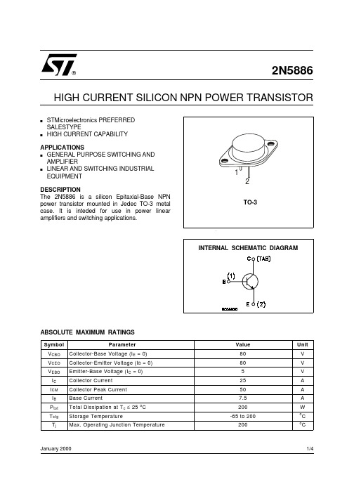
2N5886HIGH CURRENT SILICON NPN POWER TRANSISTORsSTMicroelectronics PREFERRED SALESTYPEsHIGH CURRENT CAPABILITYAPPLICATIONS s GENERAL PURPOSE SWITCHING AND AMPLIFIERs LINEAR AND SWITCHING INDUSTRIAL EQUIPMENT DESCRIPTION The 2N5886 is a silicon Epitaxial-Base NPN power transistor mounted in Jedec TO-3 metal case. It is inteded for use in power linear amplifiers and switching applications.January 2000ABSOLUTE MAXIMUM RATINGS®1/42N5886THERMAL DATAC unless otherwise specified)ELECTRICAL CHARACTERISTICS (T case = 25 o2N5886Information furnished is believed to be accurate and reliable. However, STMicroelectronics assumes no responsibility for the consequences of use of such information nor for any infringement of patents or other rights of third parties which may result from its use. No license is granted by implication or otherwise under any patent or patent rights of STMicroelectronics. Specification mentioned in this publication are subject to change without notice. This publication supersedes and replaces all information previously supplied. STMicroelectronics products are not authorized for use as critical components in life support devices or systems without express written approval of STMicroelectronics.The ST logo is a trademark of STMicroelectronics© 2000 STMicroelectronics – Printed in Italy – All Rights ReservedSTMicroelectronics GROUP OF COMPANIESAustralia - Brazil - China - Finland - France - Germany - Hong Kong - India - Italy - Japan - Malaysia - Malta - Morocco - Singapore - Spain - Sweden - Switzerland - United Kingdom - U.S.A.2N5886。
25136中文资料

CHOOSE XTRA•GUARD® 2 FOR:
s s
s s
s
s s
Now Rated To 90°C! Unmatched Resistance to Oils, Fuels, Solvents, and Water Twice the Tensile Strength of PVC Three Times the Tear and Abrasion Resistance of PVC Superior Low-Temperature Flexibility to -20° C Ultraviolet Light Stability (jacket color black) SUPRASHIELD® - Twice as Effective as Foil Shielding
24 AWG (0,23mm2), 7/32 (7x0,20mm), Insulation Thickness: 0.010" (0,25mm) Jacket Thickness Nominal Diameter Part No. No. of Pairs. Inches mm Inches mm
25271 25272 25273 25274 25275 25276 25279 25279/11 25279/15 25279/19 1 2 3 4 5 6 9 11 15 19 0.032 0.032 0.032 0.032 0.032 0.032 0.032 0.032 0.032 0.032 0,81 0,81 0,81 0,81 0,81 0,81 0,81 0,81 0,81 0,81 0.18 0.23 0.25 0.28 0.30 0.31 0.36 0.38 0.43 0.46 4,6 5,8 6,5 7,0 7,5 8,0 9,1 9,7 10,8 11,8
2n3866参数

2n3866参数(实用版)目录1.2n3866 概述2.2n3866 的主要参数3.2n3866 参数的详细说明正文2n3866 是一款常见的电子元器件,广泛应用于各种电子设备中。
了解 2n3866 的参数对于选择和使用该元器件至关重要。
下面我们将详细介绍 2n3866 的主要参数及其含义。
首先,我们来了解一下 2n3866 的基本概述。
2n3866 是一种双极型晶体管,具有放大和开关等功能。
它主要由三个区域组成:n 型区、p 型区和 n 型区,其中两个 n 型区之间夹着一个 p 型区。
这种结构使得2n3866 具有很高的电流放大能力和良好的开关特性。
接下来,我们来看一下 2n3866 的主要参数。
在查阅相关资料时,我们通常会看到以下几个参数:1.集电极电流(IC):集电极电流是晶体管工作时流经集电极的电流。
它是晶体管的一个重要参数,决定了晶体管的电流放大能力。
2.集电极 - 发射极电压(VCE):集电极 - 发射极电压是指在晶体管工作时,集电极和发射极之间的电压。
这个参数影响了晶体管的输出特性。
3.发射极电流(IE):发射极电流是指在晶体管工作时流经发射极的电流。
发射极电流与集电极电流之间有一定的关系,通常用来评价晶体管的电流放大能力。
4.功耗(PD):功耗是指晶体管在工作过程中消耗的功率。
功耗与晶体管的电流和电压有关,对晶体管的可靠性和稳定性有重要影响。
在了解了 2n3866 的主要参数后,我们还需要对这些参数进行详细说明,以便更好地理解和应用这款元器件。
以下是 2n3866 参数的详细说明:1.集电极电流(IC):集电极电流是 2n3866 最重要的参数之一。
根据不同的使用场景,我们可以选择具有不同集电极电流的 2n3866。
通常情况下,集电极电流越大,晶体管的电流放大能力越强。
2.集电极 - 发射极电压(VCE):集电极 - 发射极电压决定了晶体管的开关速度。
在实际应用中,我们需要根据电路的要求选择合适的 VCE 值。
AN2526NFH资料
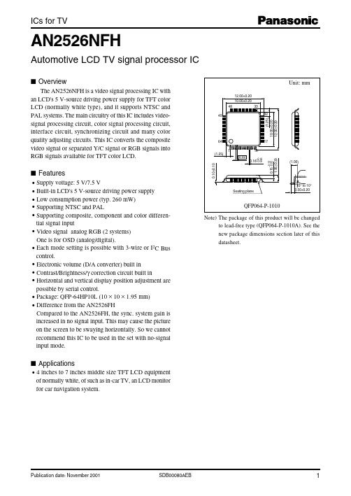
AN2526NFH
Automotive LCD TV signal processor IC
I Overview
The AN2526NFH is a video signal processing IC with an LCD's 5 V-source driving power supply for TFT color LCD (normally white type), and it supports NTSC and PAL systems. The main circuitry of this IC includes videosignal processing circuit, color signal processing circuit, interface circuit, synchronizing circuit and many color quality adjusting circuits. This IC converts the composite video signal or separated Y/C signal or RGB signals into RGB signals available for TFT color LCD.
1 µF 5.1 kΩ NTSC 3.58 MHz PAL 4.43 MHz 0.1 µF
56
VXO
57
58
CLMP (BGP)
R-out
Trap
GND 3
59
GND1 21GBiblioteka mma4.7 µF60
YAP ctl.
VCC1
50 kB
R−Y out
61
20 19
2N5566中文资料

Unit
V mA pA nA pA nA W V
mS mS mS
pF nV⁄ √Hz dB
mV mV/ _C
dB NCBD
8-2
Document Number: 70254 S-04031—Rev. D, 04-Jun-01
元器件交易网
2N5564/5565/5566
元器件交易网
2N5564/5565/5566
Vishay Siliconix
Matched N-Channel JFET Pairs
PRODUCT SUMMARY
Part Number
2N5564 2N5565 2N5566
VGS(off) (V)
–0.5 to –3 –0.5 to –3 –0.5 to –3
76
Notes a. Typical values are for DESIGN AID ONLY, not guaranteed nor subject to production testing.
b. Pulse test: PW v300 ms duty cycle v3%. c. This parameter not registered with JEDEC.
160
0 –10
rDS(on) – Drain-Source On-Resistance ( W )
120 VGS(off) = –2 V
80
40
gfs – Forward Transconductance (mS)
0 –55 –35 –15 5
APPLICATIONS
D Wideband Differential Amps D High-Speed,
LM2586_05资料
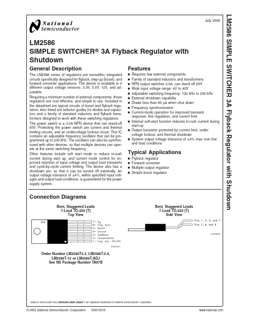
LM2586SIMPLE SWITCHER ®3A Flyback Regulator with ShutdownGeneral DescriptionThe LM2586series of regulators are monolithic integrated circuits specifically designed for flyback,step-up (boost),and forward converter applications.The device is available in 4different output voltage versions:3.3V,5.0V,12V,and ad-justable.Requiring a minimum number of external components,these regulators are cost effective,and simple to use.Included in the datasheet are typical circuits of boost and flyback regu-lators.Also listed are selector guides for diodes and capaci-tors and a family of standard inductors and flyback trans-formers designed to work with these switching regulators.The power switch is a 3.0A NPN device that can stand-off 65V.Protecting the power switch are current and thermal limiting circuits,and an undervoltage lockout circuit.This IC contains an adjustable frequency oscillator that can be pro-grammed up to 200kHz.The oscillator can also be synchro-nized with other devices,so that multiple devices can oper-ate at the same switching frequency.Other features include soft start mode to reduce in-rush current during start up,and current mode control for im-proved rejection of input voltage and output load transients and cycle-by-cycle current limiting.The device also has a shutdown pin,so that it can be turned off externally.An output voltage tolerance of ±4%,within specified input volt-ages and output load conditions,is guaranteed for the power supply system.Featuresn Requires few external componentsn Family of standard inductors and transformers n NPN output switches 3.0A,can stand off 65V n Wide input voltage range:4V to 40Vn Adjustable switching frequency:100kHz to 200kHz n External shutdown capabilityn Draws less than 60µA when shut down n Frequency synchronizationnCurrent-mode operation for improved transient response,line regulation,and current limitn Internal soft-start function reduces in-rush current during start-upn Output transistor protected by current limit,under voltage lockout,and thermal shutdownn System output voltage tolerance of ±4%max over line and load conditions Typical Applicationsn Flyback regulator n Forward convertern Multiple-output regulator nSimple boost regulatorConnection DiagramsBent,Staggered Leads 7-Lead TO-220(T)Top ViewBent,Staggered Leads 7-Lead TO-220(T)Side View0125161701251618Order Number LM2586T3.3,LM2586T-5.0,LM2586T-12or LM2586T-ADJ See NS Package Number TA07BSIMPLE SWITCHER ®and Switchers Made Simple®are registered trademarks of National Semiconductor Corporation.July 2005LM2586SIMPLE SWITCHER 3A Flyback Regulator with Shutdown©2005National Semiconductor Corporation Connection Diagrams(Continued)7-Lead TO-263(S)Top View7-Lead TO-263(S)Side View0125161901251620Order number LM2586S-3.3,LM2586S-5.0,LM2586S-12or LM2586S-ADJTape and Reel Order Number LM2586SX-3.3,LM2586SX-5.0,LM2586SX-12or LM2586SX-ADJSee NS Package Number TS7BOrdering InformationPackage TypeNSC Package Order NumberDrawing 7-Lead TO-220Bent,Staggered Leads TA07B LM2586T-3.3,LM2586T-5.0,LM2586T-12,LM2586T-ADJ 7-Lead TO-263TS7B LM2586S-3.3,LM2586S-5.0,LM2586S-12,LM2586S-ADJ 7-Lead TO-263Tape and ReelTS7BLM2586SX-3.3,LM2586SX-5.0,LM2586SX-12,LM2586SX-ADJL M 2586 2Absolute Maximum Ratings(Note1)If Military/Aerospace specified devices are required, please contact the National Semiconductor Sales Office/ Distributors for availability and specifications.Input Voltage−0.4V≤V IN≤45V Switch Voltage−0.4V≤V SW≤65V Switch Current(Note2)Internally Limited Compensation Pin Voltage−0.4V≤V COMP≤2.4V Feedback Pin Voltage−0.4V≤V FB≤2V OUT ON/OFF Pin Voltage−0.4V≤V SH≤6V Sync Pin Voltage−0.4V≤V SYNC≤2V Power Dissipation(Note3)Internally Limited Storage Temperature Range−65˚C to+150˚CLead Temperature(Soldering,10sec.)260˚C Maximum Junction Temperature(Note3)150˚C Minimum ESD Rating(C=100pF,R=1.5kΩ)2kVOperating RatingsSupply Voltage4V≤V IN≤40V Output Switch Voltage0V≤V SW≤60V Output Switch Current I SW≤3.0A Junction Temp.Range−40˚C≤T J≤+125˚CElectrical CharacteristicsSpecifications with standard type face are for T J=25˚C,and those in bold type face apply over full Operating Temperature Range.Unless otherwise specified,V IN=5V.LM2586-3.3Symbol Parameters Conditions Typical Min Max Units SYSTEM PARAMETERS Test Circuit of Figure1(Note4)V OUT Output Voltage V IN=4V to12V 3.3 3.17/3.14 3.43/3.46VI LOAD=0.3to1.2A∆V OUT/Line Regulation V IN=4V to12V2050/100mV ∆V IN I LOAD=0.3A∆V OUT/Load Regulation V IN=12V2050/100mV ∆I LOAD I LOAD=0.3A to1.2AηEfficiency V IN=5V,I LOAD=0.3A76% UNIQUE DEVICE PARAMETERS(Note5)V REF Output Reference Measured at Feedback Pin 3.3 3.242/3.234 3.358/3.366V Voltage V COMP=1.0V∆V REF Reference Voltage V IN=4V to40V 2.0mV Line RegulationG M Error Amp I COMP=−30µA to+30µA 1.1930.678 2.259mmhoTransconductance V COMP=1.0VA VOL Error Amp V COMP=0.5V to1.6V260151/75V/VVoltage Gain R COMP=1.0MΩ(Note6)LM2586-5.0Symbol Parameters Conditions Typical Min Max Units SYSTEM PARAMETERS Test Circuit of Figure1(Note4)V OUT Output Voltage V IN=4V to12V 5.0 4.80/4.75 5.20/5.25VI LOAD=0.3A to1.1A∆V OUT/Line Regulation V IN=4V to12V2050/100mV ∆V IN I LOAD=0.3A∆V OUT/Load Regulation V IN=12V2050/100mV ∆I LOAD I LOAD=0.3A to1.1AηEfficiency V IN=12V,I LOAD=0.6A80% UNIQUE DEVICE PARAMETERS(Note5)V REF Output ReferenceVoltage Measured at Feedback PinV COMP=1.0V5.0 4.913/4.900 5.088/5.100VLM25863Electrical Characteristics (Continued)LM2586-5.0(Continued)Symbol Parameters ConditionsTypical Min Max Units ∆V REF Reference Voltage V IN =4V to 40V3.3mVLine Regulation G M Error Amp I COMP =−30µA to +30µA 0.7500.447 1.491mmho Transconductance V COMP =1.0V A VOLError Amp V COMP =0.5V to 1.6V 16599/49V/VVoltage GainR COMP =1.0M Ω(Note 6)LM2586-12Symbol Parameters ConditionsTypical Min Max Units SYSTEM PARAMETERS Test Circuit of Figure 2(Note 4)V OUT Output Voltage V IN =4V to 10V 12.011.52/11.4012.48/12.60VI LOAD =0.2A to 0.8A ∆V OUT /Line RegulationV IN =4V to 10V 20100/200mV∆V IN I LOAD =0.2A ∆V OUT /Load RegulationV IN =10V20100/200mV∆I LOAD I LOAD =0.2A to 0.8A ηEfficiency V IN =10V,I LOAD =0.6A 93%UNIQUE DEVICE PARAMETERS (Note 5)V REF Output Reference Measured at Feedback Pin 12.011.79/11.7612.21/12.24VVoltageV COMP =1.0V ∆V REF Reference Voltage V IN =4V to 40V7.8mVLine Regulation G M Error Amp I COMP =−30µA to +30µA 0.3280.1860.621mmhoTransconductance V COMP =1.0V A VOLError Amp V COMP =0.5V to 1.6V 7041/21V/VVoltage GainR COMP =1.0M Ω(Note 6)LM2586-ADJSymbol ParametersConditionsTypical Min Max Units SYSTEM PARAMETERS Test Circuit of Figure 2(Note 4)V OUT Output Voltage V IN =4V to 10V 12.011.52/11.4012.48/12.60VI LOAD =0.2A to 0.8A ∆V OUT /Line RegulationV IN =4V to 10V 20100/200mV∆V IN I LOAD =0.2A ∆V OUT /Load RegulationV IN =10V20100/200mV∆I LOAD I LOAD =0.2A to 0.8A ηEfficiency V IN =10V,I LOAD =0.6A 93%UNIQUE DEVICE PARAMETERS (Note 5)V REF Output Reference Measured at Feedback Pin 1.2301.208/1.2051.252/1.255VVoltageV COMP =1.0V ∆V REF Reference Voltage V IN =4V to 40V1.5mVLine Regulation G M Error Amp I COMP =−30µA to +30µA 3.2001.8006.000mmhoTransconductance V COMP =1.0VA VOLError Amp Voltage GainV COMP =0.5V to 1.6V,R COMP =1.0M Ω(Note 6)670400/200V/VL M 2586 4LM2586 Electrical Characteristics(Continued)LM2586-ADJ(Continued)Symbol Parameters Conditions Typical Min Max UnitsI B Error Amp V COMP=1.0V125425/600nAInput Bias CurrentCOMMON DEVICE PARAMETERS for all versions(Note5)I S Input Supply Current Switch Off(Note8)1115.5/16.5mAI SWITCH=1.8A50100/115mAI S/D Shutdown Input V SH=3V16100/300µASupply CurrentV UV Input Supply R LOAD=100Ω 3.30 3.05 3.75V Undervoltage Lockoutf O Oscillator Frequency Measured at Switch PinR LOAD=100Ω,V COMP=1.0V10085/75115/125kHzFreq.Adj.Pin Open(Pin1)R SET=22kΩ200kHzf SC Short-Circuit Measured at Switch PinFrequency R LOAD=100Ω25kHzV FEEDBACK=1.15VV EAO Error Amplifier Upper Limit 2.8 2.6/2.4V Output Swing(Note7)Lower Limit0.250.40/0.55V(Note8)I EAO Error Amp(Note9)Output Current165110/70260/320µA(Source or Sink)I SS Soft Start Current V FEEDBACK=0.92V11.08.0/7.017.0/19.0µAV COMP=1.0VD MAX Maximum Duty Cycle R LOAD=100Ω9893/90%(Note7)I L Switch Leakage Switch Off15300/600µACurrent V SWITCH=60VV SUS Switch Sustaining Voltage dV/dT=1.5V/ns65VV SAT Switch Saturation Voltage I SWITCH=3.0A0.450.65/0.9VI CL NPN Switch Current Limit 4.0 3.07.0AV STH Synchronization F SYNC=200kHz0.750.625/0.400.875/1.00V Threshold Voltage V COMP=1V,V IN=5VI SYNC Synchronization V IN=5V100200µAPin Current V COMP=1V,V SYNC=V STHV SHTH ON/OFF Pin(Pin1)V COMP=1V 1.6 1.0/0.8 2.2/2.4V Threshold Voltage(Note10)I SH ON/OFF Pin(Pin1)V COMP=1V4015/1065/75µACurrent V SH=V SHTH5Electrical Characteristics (Continued)LM2586-ADJ(Continued)Symbol ParametersConditionsTypical Min Max UnitsCOMMON DEVICE PARAMETERS for all versions (Note 5)θJA Thermal ResistanceT Package,Junction to Ambient (Note 11)65˚C/WθJA T Package,Junction to Ambient (Note 12)45θJC T Package,Junction to Case 2θJA S Package,Junction to Ambient (Note 13)56θJA S Package,Junction to Ambient (Note 14)35θJA S Package,Junction to Ambient (Note 15)26θJCS Package,Junction to Case2Note 1:Absolute Maximum Ratings indicate limits beyond which damage to the device may occur.These ratings apply when the current is limited to less than 1.2mA for pins 1,2,3,and 6.Operating ratings indicate conditions for which the device is intended to be functional,but device parameter specifications may not be guaranteed under these conditions.For guaranteed specifications and test conditions,see the Electrical Characteristics.Note 2:Note that switch current and output current are not identical in a step-up regulator.Output current cannot be internally limited when the LM2586is used as a step-up regulator.To prevent damage to the switch,the output current must be externally limited to 3A.However,output current is internally limited when the LM2586is used as a flyback regulator (see the Application Hints section for more information).Note 3:The junction temperature of the device (T J )is a function of the ambient temperature (T A ),the junction-to-ambient thermal resistance (θJA ),and the power dissipation of the device (P D ).A thermal shutdown will occur if the temperature exceeds the maximum junction temperature of the device:P D x θJA +T A(MAX)≥T J(MAX).For a safe thermal design,check that the maximum power dissipated by the device is less than:P D ≤[T J(MAX)−T A(MAX)]/θJA .When calculating the maximum allowable power dissipation,derate the maximum junction temperature —this ensures a margin of safety in the thermal design.Note 4:External components such as the diode,inductor,input and output capacitors can affect switching regulator performance.When the LM2586is used as shown in Figures 1,2,system performance will be as specified by the system parameters.Note 5:All room temperature limits are 100%production tested,and all limits at temperature extremes are guaranteed via correlation using standard Statistical Quality Control (SQC)methods.Note 6:A 1.0M Ωresistor is connected to the compensation pin (which is the error amplifier output)to ensure accuracy in measuring A VOL .Note 7:To measure this parameter,the feedback voltage is set to a low value,depending on the output version of the device,to force the error amplifier output high and the switch on.Note 8:To measure this parameter,the feedback voltage is set to a high value,depending on the output version of the device,to force the error amplifier output low and the switch off.Note 9:To measure the worst-case error amplifier output current,the LM2586is tested with the feedback voltage set to its low value (Note 7)and at its high value (Note 8).Note 10:When testing the minimum value,do not sink current from this pin —isolate it with a diode.If current is drawn from this pin,the frequency adjust circuit will begin operation (see Figure 41).Note 11:Junction to ambient thermal resistance (no external heat sink)for the 7lead TO-220package mounted vertically,with 1⁄2inch leads in a socket,or on a PC board with minimum copper area.Note 12:Junction to ambient thermal resistance (no external heat sink)for the 7lead TO-220package mounted vertically,with 1⁄2inch leads soldered to a PC board containing approximately 4square inches of (1oz.)copper area surrounding the leads.Note 13:Junction to ambient thermal resistance for the 7lead TO-263mounted horizontally against a PC board area of 0.136square inches (the same size as the TO-263package)of 1oz.(0.0014in.thick)copper.Note 14:Junction to ambient thermal resistance for the 7lead TO-263mounted horizontally against a PC board area of 0.4896square inches (3.6times the area of the TO-263package)of 1oz.(0.0014in.thick)copper.Note 15:Junction to ambient thermal resistance for the 7lead TO-263mounted horizontally against a PC board copper area of 1.0064square inches (7.4times the area of the TO-263package)of 1oz.(0.0014in.thick)copper.Additional copper area will reduce thermal resistance further.See the thermal model in Switchers Made Simple ®software.L M 2586 6Typical Performance CharacteristicsSupply Current vs TemperatureReference Voltage vs Temperature0125160201251603∆Reference Voltage vs Supply Voltage Supply Current vs Switch Current0125160401251605Current Limit vs Temperature Feedback Pin Bias Current vs Temperature0125160601251607LM25867Typical Performance Characteristics(Continued)Switch Saturation Voltage vs TemperatureSwitch Transconductancevs Temperature0125160801251609Oscillator Frequency vs Temperature Error Amp Transconductancevs Temperature0125161001251611Error Amp Voltage Gain vs Temperature Short Circuit Frequencyvs Temperature0125161201251613L M 2586 8Typical Performance Characteristics(Continued)Shutdown Supply Currentvs TemperatureON/OFF Pin Currentvs Voltage0125161401251615Oscillator Frequencyvs Resistance01251616Flyback Regulator01251601LM25869Test Circuits01251621C IN1—100µF,25V Aluminum Electrolytic C IN2—0.1µF CeramicT —22µH,1:1Schott #67141450D —1N5820C OUT —680µF,16V Aluminum Electrolytic C C —0.47µF Ceramic R C —2kFIGURE 1.LM2586-3.3and LM2586-5.001251622C IN1—100µF,25V Aluminum Electrolytic C IN2—0.1µF Ceramic L —15µH,Renco #RL-5472-5D —1N5820C OUT —680µF,16V Aluminum Electrolytic C C —0.47µF Ceramic R C —2kFor 12V Devices:R1=Short (0Ω)and 2=OpenFor ADJ Devices:R1=48.75k,±0.1%and 2=5.62k,±0.1%FIGURE 2.LM2586-12and LM2586-ADJL M 2586 10Flyback Regulator OperationThe LM2586is ideally suited for use in the flyback regulator topology.The flyback regulator can produce a single output voltage,such as the one shown in Figure4,or multiple output voltages.In Figure4,the flyback regulator generates an output voltage that is inside the range of the input voltage. This feature is unique to flyback regulators and cannot be duplicated with buck or boost regulators.The operation of a flyback regulator is as follows(refer to Figure4):when the switch is on,current flows through the primary winding of the transformer,T1,storing energy in the magnetic field of the transformer.Note that the primary and secondary windings are out of phase,so no current flows through the secondary when current flows through the pri-mary.When the switch turns off,the magnetic field col-lapses,reversing the voltage polarity of the primary and secondary windings.Now rectifier D1is forward biased and current flows through it,releasing the energy stored in the transformer.This produces voltage at the output.The output voltage is controlled by modulating the peak switch current.This is done by feeding back a portion of the output voltage to the error amp,which amplifies the differ-ence between the feedback voltage and a1.230V reference. The error amp output voltage is compared to a ramp voltage proportional to the switch current(i.e.,inductor current dur-ing the switch on time).The comparator terminates the switch on time when the two voltages are equal,thereby controlling the peak switch current to maintain a constant output voltage.Block Diagram01251623 For Fixed Versions3.3V,R1=3.4k,R2=2k5.0V,R1=6.15k,R2=2k12V,R1=8.73k,R2=1kFor Adj.VersionR1=Short(0Ω),R2=OpenFIGURE3.Block Diagram LM2586Flyback Regulator Operation(Continued)Typical Performance Characteristics01251624As shown in Figure 4,the LM2586can be used as a flyback regulator by using a minimum number of external components.The switching waveforms of this regulator are shown in Figure 5.Typical Performance Characteristics observed during the operation of this circuit are shown in Figure 6.FIGURE 4.12V Flyback Regulator Design Example01251665A:Switch Voltage,20V/div B:Switch Current,2A/divC:Output Rectifier Current,2A/divD:Output Ripple Voltage,50mV/div AC-CoupledFIGURE 5.Switching WaveformsL M 2586Typical Performance Characteristics(Continued)Typical Flyback Regulator ApplicationsFigure 7through Figure 12show six typical flyback applica-tions,varying from single output to triple output.Each draw-ing contains the part number(s)and manufacturer(s)for every component except the transformer.For the trans-former part numbers and manufacturers’names,see thetable in Figure 13.For applications with different output voltages —requiring the LM2586-ADJ —or different output configurations that do not match the standard configurations,refer to the Switchers Made Simple software.01251666FIGURE 6.V OUT Response to Load Current Step01251627FIGURE 7.Single-Output Flyback RegulatorLM2586Typical Flyback Regulator Applications(Continued)01251628FIGURE 8.Single-Output Flyback Regulator01251629FIGURE 9.Single-Output Flyback RegulatorL M 2586Typical Flyback Regulator Applications(Continued)01251630FIGURE10.Dual-Output Flyback Regulator01251631FIGURE11.Dual-Output Flyback Regulator LM2586Typical Flyback Regulator Applications(Continued)TRANSFORMER SELECTION (T)Figure 13lists the standard transformers available for fly-back regulator applications.Included in the table are the turns ratio(s)for each transformer,as well as the output voltages,input voltage ranges,and the maximum load cur-rents for each circuit.01251632FIGURE 12.Triple-Output Flyback RegulatorApplications Figure 7Figure 8Figure 9Figure 10Figure 11Figure 12Transformers T7T7T7T6T6T5V IN 4V–6V 4V–6V 8V–16V 4V–6V 18V–36V 18V–36V V OUT1 3.3V 5V 12V 12V 12V 5V I OUT1(Max) 1.4A 1A 0.8A 0.15A 0.6A 1.8A N 11111.2 1.20.5V OUT2−12V −12V 12V I OUT2(Max)0.15A 0.6A 0.25A N 2 1.21.21.15V OUT3−12V I OUT3(Max)0.25A N 31.15FIGURE 13.Transformer Selection TableL M 2586Typical Flyback Regulator Applications(Continued)TRANSFORMER FOOTPRINTSFigure15through Figure29show the footprints of eachtransformer,listed in Figure14.TransformerTypeManufacturers’Part NumbersCoilcraft(Note16)Coilcraft(Note16)SurfaceMountPulse(Note17)Surface MountPulse(Note17)Renco(Note18)Schott(Note19)T5Q4338-B Q4437-B PE-68413—RL-553267140890T6Q4339-B Q4438-B PE-68414—RL-553367140900T7S6000-A S6057-A—PE-68482RL-575126606Note16:Coilcraft Inc.,Phone:(800)322-26451102Silver Lake Road,Cary,IL60013Fax:(708)639-1469European Headquarters,21Napier Place Phone:+441236730595Wardpark North,Cumbernauld,Scotland G680LL Fax:+441236730627Note17:Pulse Engineering Inc.,Phone:(619)674-810012220World Trade Drive,San Diego,CA92128Fax:(619)674-8262European Headquarters,Dunmore Road Phone:+3539324107Tuam,Co.Galway,Ireland Fax:+3539324459Note18:Renco Electronics Inc.,Phone:(800)645-582860Jeffryn Blvd.East,Deer Park,NY11729Fax:(516)586-5562Note19:Schott Corp.,Phone:(612)475-11731000Parkers Lane Road,Wayzata,MN55391Fax:(612)475-1786FIGURE14.Transformer Manufacturer GuideT701251633Top ViewFIGURE15.Coilcraft S6000-AT601251634Top ViewFIGURE16.Coilcraft Q4339-BT501251635FIGURE17.Coilcraft Q4437-B(Surface Mount)T501251636Top ViewFIGURE18.Coilcraft Q4338-BLM2586Typical Flyback RegulatorApplications(Continued)T701251637Top ViewFIGURE19.Coilcraft S6057-A(Surface Mount)T601251638Top ViewFIGURE20.Coilcraft Q4438-B(Surface Mount)T701251639Top ViewFIGURE21.Pulse PE-68482T601251640Top ViewFIGURE22.Pulse PE-68414(Surface Mount)T501251642Top ViewFIGURE23.Pulse PE-68413(Surface Mount)T701251643Top ViewFIGURE24.Renco RL-5751T601251645Top ViewFIGURE25.Renco RL-5533T501251646Top ViewFIGURE26.Renco RL-5532LM2586Typical Flyback Regulator Applications(Continued)Step-Up (Boost)Regulator OperationFigure 30shows the LM2586used as a step-up (boost)regulator.This is a switching regulator that produces an output voltage greater than the input supply voltage.A brief explanation of how the LM2586Boost Regulator works is as follows (refer to Figure 30).When the NPN switch turns on,the inductor current ramps up at the rate of V IN /L,storing energy in the inductor.When the switch turns off,the lower end of the inductor flies above V IN ,discharging its current through diode (D)into the output capacitor (C OUT )at a rate of (V OUT −V IN )/L.Thus,energy stored in the inductor during the switch on time is transferred to the output during the switch off time.The output voltage is controlled by adjusting the peak switch current,as described in the flyback regulator section.T701251647Top ViewFIGURE 27.Schott 26606T601251649Top ViewFIGURE 28.Schott 67140900T501251650Top ViewFIGURE 29.Schott 67140890LM2586Step-Up (Boost)Regulator Operation(Continued)By adding a small number of external components (as shown in Figure 30),the LM2586can be used to produce a regulated output voltage that is greater than the applied inputvoltage.The switching waveforms observed during the op-eration of this circuit are shown in Figure 31.Typical perfor-mance of this regulator is shown in Figure 32.01251651FIGURE 30.12V Boost RegulatorL M 2586Typical Performance CharacteristicsTypical Boost Regulator ApplicationsFigures 33,35through Figure 37show four typical boost applications —one fixed and three using the adjustable ver-sion of the LM2586.Each drawing contains the part num-ber(s)and manufacturer(s)for every component.For the fixed 12V output application,the part numbers and manufac-turers’names for the inductor are listed in a table in Figure 34.For applications with different output voltages,refer to the Switchers Made Simple software.01251667A:Switch Voltage,10V/div B:Switch Current,2A/div C:Inductor Current,2A/divD:Output Ripple Voltage,100mV/div,AC-CoupledFIGURE 31.Switching Waveforms01251668FIGURE 32.V OUT Response to Load Current StepLM258621Typical Boost Regulator Applications(Continued)Figure 34contains a table of standard inductors,by part number and corresponding manufacturer,for the fixed out-put regulator of Figure 33.01251654FIGURE 33.+5V to +12V Boost RegulatorCoilcraft (Note 20)Pulse (Note 21)Renco (Note 22)Schott (Note 23)Schott (Note 23)(Surface Mount)DO3316-153PE-53898RL-5471-76714651067146540Note 20:Coilcraft Inc.,Phone:(800)322-26451102Silver Lake Road,Cary,IL 60013Fax:(708)639-1469European Headquarters,21Napier Place Phone:+441236730595Wardpark North,Cumbernauld,Scotland G680LL Fax:+441236730627Note 21:Pulse Engineering Inc.,Phone:(619)674-810012220World Trade Drive,San Diego,CA 92128Fax:(619)674-8262European Headquarters,Dunmore Road Phone:+3539324107Tuam,Co.Galway,Ireland Fax:+3539324459Note 22:Renco Electronics Inc.,Phone:(800)645-582860Jeffryn Blvd.East,Deer Park,NY 11729Fax:(516)586-5562Note 23:Schott Corp.,Phone:(612)475-11731000Parkers Lane Road,Wayzata,MN 55391Fax:(612)475-1786FIGURE 34.Inductor Selection TableL M 2586 22Typical Boost Regulator Applications(Continued)01251655FIGURE 35.+12V to +24V Boost Regulator01251656FIGURE 36.+24V to +36V Boost RegulatorLM258623Typical Boost Regulator Applications(Continued)Note 24:The LM2586will require a heat sink in these applications.The size of the heat sink will depend on the maximum ambient temperature.To calculate the thermal resistance of the IC and the size of the heat sink needed,see the “Heat Sink/Thermal Considerations”section in the Applica-tion Hints.Application HintsLM2586SPECIAL FEATURESSHUTDOWN CONTROLA feature of the LM2586is its ability to be shut down using the ON /OFF pin (pin 1).This feature conserves input power by turning off the device when it is not in use.For proper operation,an isolation diode is required (as shown in Figure 38).The device will shut down when 3V or greater is applied on the ON /OFF pin,sourcing current into pin 1.In shut down mode,the device will draw typically 56µA of supply current (16µA to V IN and 40µA to the ON /OFF pin).To turn the device back on,leave pin 1floating,using an (isolation)diode,as shown in Figure 38(for normal operation,do not source or sink current to or from this pin —see the next section).FREQUENCY ADJUSTMENTThe switching frequency of the LM2586can be adjusted with the use of an external resistor.This feature allows the user to optimize the size of the magnetics and the output capaci-tor(s)by tailoring the operating frequency.A resistor con-nected from pin 1(the Freq.Adj.pin)to ground will set the switching frequency from 100kHz to 200kHz (maximum).As shown in Figure 38,the pin can be used to adjust the frequency while still providing the shut down function.A curve in the Performance Characteristics Section graphs the resistor value to the corresponding switching frequency.The table in Figure 39shows resistor values corresponding to commonly used frequencies.However,changing the LM2586’s operating frequency from its nominal value of 100kHz will change the magnetics selection and compensation component values.01251657FIGURE 37.+24V to +48V Boost Regulator01251658FIGURE 38.Shutdown OperationL M 2586 24Application Hints(Continued)FREQUENCY SYNCHRONIZATIONAnother feature of the LM2586is the ability to synchronizethe switching frequency to an external source,using thesync pin(pin6).This feature allows the user to parallelmultiple devices to deliver more output power.A negative falling pulse applied to the sync pin will synchro-nize the LM2586to an external oscillator(see Figures40,41).Use of this feature enables the LM2586to be synchronizedto an external oscillator,such as a system clock.This opera-tion allows multiple power supplies to operate at the samefrequency,thus eliminating frequency-related noise prob-lems.The scope photo in Figure41shows a LM258612V BoostRegulator synchronized to a200kHz signal.There is a700ns delay between the falling edge of the sync signal and theturning on of the switch.PROGRAMMING OUTPUT VOLTAGE(SELECTING R1AND R2)Referring to the adjustable regulator in Figure42,the outputvoltage is programmed by the resistors R1and R2by thefollowing formula:V OUT=V REF(1+R1/R2)where V REF=1.23VResistors R1and R2divide the output voltage down so thatit can be compared with the1.23V internal reference.WithR2between1k and5k,R1is:R1=R2(V OUT/V REF−1)where V REF=1.23VFor best temperature coefficient and stability with time,use1%metal film resistors.SHORT CIRCUIT CONDITIONDue to the inherent nature of boost regulators,when theoutput is shorted(see Figure42),current flows directly fromthe input,through the inductor and the diode,to the output,bypassing the switch.The current limit of the switch does notlimit the output current for the entire circuit.To protect theload and prevent damage to the switch,the current must beexternally limited,either by the input supply or at the output R SET(kΩ)Frequency(kHz)Open100200125471503317522200FIGURE39.Frequency Setting Resistor Guide01251659FIGURE40.Frequency Synchronization01251669FIGURE41.Waveforms of a Synchronized12V Boost Regulator01251661FIGURE42.Boost RegulatorLM258625。
UL2556中文翻译

UL2556 2011译版通过UL UL安全标准的保护。
既不是一个标准的打印副本,也分布一个标准的软盘和分布软盘上的标准文件的软盘应以任何方式改变。
所有UL的标准和所有,所有权,和权利有关这些标准应保持了UL的唯一和排他性的财产。
保留所有权利。
本出版物的任何部分进行复制,存储在检索系统中,或任何形式的任何手段,电子,机械复印,录音,或以其他方式传播未经事先批准的UL。
UL安全标准的修订,不时发出。
一个是最新的UL安全标准只有当它采用了最近通过的修订。
UL提供本标准平方米²,没有任何形式的的担保,明示或暗示,包括但不限于对适销性或为任何目的的隐含担保。
在任何情况下,UL认证的任何特殊,偶然,必然,间接或类似的损害承担责任,包括利润损失,储蓄损失,数据丢失,或任何因使用或其他损害无法使用这个标准,即使UL或授权的UL代表的建议这种损害的可能性。
在任何情况下,UL的任何损害赔偿责任,不断超过支付的价格这个标准,无论索赔的形式。
UL将尝试回答有关其标准的电子版本的支持请求。
然而,这支持服务是提供一个合理的努力的基础上,和UL未必能解决所有支持请求。
只有他们正在使用的UL认证支持其标准的电子版本条件和操作系统,它的目的是。
UL的扶持政策可能会改变时间到时,恕不另行通知。
UL保留权利更改的格式,简报,文件类型和格式,交货方式和格式,和它的印刷版和电子标准,恕不另行通知。
UL安全标准的电子版本,买方同意维护,保障,并举行UL认证无害和反对任何损失,费用,责任,损失,索赔,或判决(包括合理的律师费)引入任何错误或偏差造成的,而买方存储购买者的计算机系统上的电子标准。
如果购买一个单用户版电子标准,本标准的一个副本可以存储在一台个人计算机的硬盘,或在一个单一的局域网的文件服务器或永久存储在这种方式的多用户电脑设备,这一标准只能由一个用户访问的时间和为没有多个并发访问的可能性。
如果多用户版电子标准购买,可以存储在一个标准的副本一个单一的局域网文件服务器,或在多用户计算机的永久性存储设备,或Intranet 服务器。
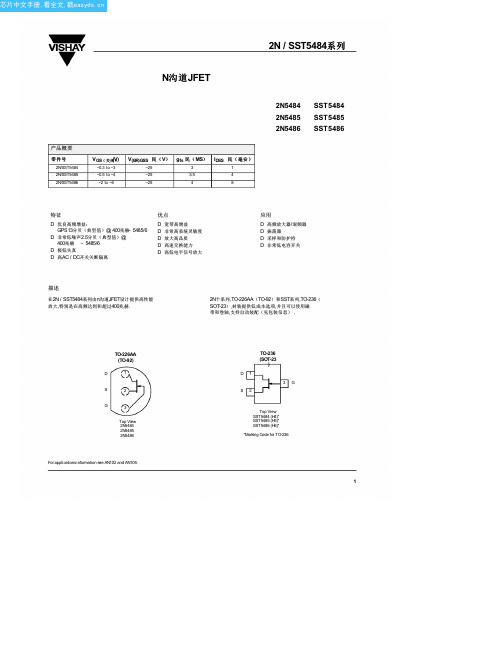
2N5484中文资料(vishay)中文数据手册「EasyDatasheet - 矽搜」
I = 10 mA , V = 0 V
−35 −25
−25
−25
V
−0.3 −3 −0.5 −4 −2 −6
1
5
4
10 8 20 mA
−0.002 −0.2
−1
−1
−1
nA
−200
−200
−200
−20
pA
0.8
V
g V = 15 V, V = 0 V f = 1 kHz
Noise Figgure
V = 15 V, I = 1 mA
NF
R = 1 kW, f = 100 MHz
V = 15 V I = 4 mA R = 1 kW
f = 100 MHz f = 400 MHz
Notes a. Typical valuesare for DESIGN AID ONLY, not guaranteed nor subject to production testing.
80 gos − Output Conductance (µS)
e
V = 15 V, V = 0 V f = 100 Hz
高频
Common-Source Transconductance
Y
f = 100 MHz f = 400 MHz
Common-Source Output Conductance
Y
V = 15 V V =0V
f = 100 MHz f = 400 MHz
5.5
45 mS
65
0.05 mS
0.8
20
21 13
0.3
dB
2SD2568中文资料(rohm)中文数据手册「EasyDatasheet - 矽搜」
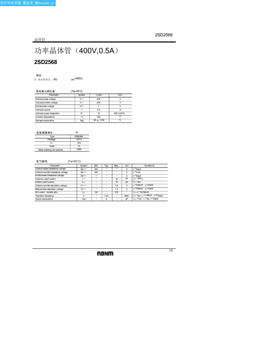
0.5 (A)
1
0.5 (A)
1
0.02 BASE SATURATION VOLTAGE : V 0.01 0.001 0.002 0.005 0.01 0.02 0.05 0.1 0.2 COLLECTOR CURRENT : I
C
0.5 (A)
1
COLLECTOR CURRENT : I
图4 DC电流增益 - 集电极电流(
1/2
芯片中文手册,看全文,戳
2SD2568
晶体管电气特Biblioteka 曲线200 (mA) 160
C
Ta=25 C
mA 3.0m A 2.5m A 2.0m A 1.5m A
1 (A)
C
V CE =3V
FE
1000 500 200 100
Ta=25 C
0.5 0.2 0.1 0.05
25°C
FE
2SD2568 CPT3 PQ TL 2500
电气特性
Parameter Collector-base breakdown voltage Collector-emitter breakdown voltage Emitter-base breakdown voltage Collector cutoff current Emitter cutoff current Collector-emitter saturation voltage Base-emitter saturation voltage DC current transfer ratio Transition frequency Output capacitance
(V) 2
BE(sat)
200 100 50 20
2N5486中文资料
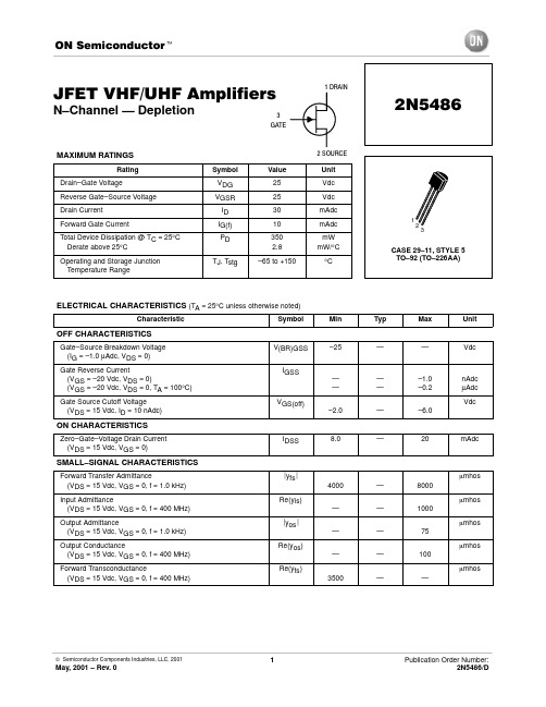
SMALL–SIGNAL CHARACTERISTICS (continued)
Input Capacitance (VDS = 15 Vdc, VGS = 0, f = 1.0 MHz) Reverse Transfer Capacitance (VDS = 15 Vdc, VGS = 0, f = 1.0 MHz) Output Capacitance (VDS = 15 Vdc, VGS = 0, f = 1.0 MHz) Ciss Crss Coss — — — — — — 5.0 1.0 2.0 pF pF pF
OFF CHARACTERISTICS
Gate–Source Breakdown Voltage (IG = –1.0 µAdc, VDS = 0) Gate Reverse Current (VGS = –20 Vdc, VDS = 0) (VGS = –20 Vdc, VDS = 0, TA = 100°C) Gate Source Cutoff Voltage (VDS = 15 Vdc, ID = 10 nAdc) V(BR)GSS IGSS — — VGS(off) –2.0 — –6.0 — — –1.0 –0.2 nAdc µAdc Vdc –25 — — Vdc
S–PARAMETERS (VDS = 15 Vdc, Tchannel = 25°C, Data Points in MHz)
30° 40° 20° 10° 0° 1.0 350° 100 100 50° 0.9 200 300 60° 70° 80° 90° 100° 110° 120° 0.8 ID = IDSS 400 500 600 0.6 900 800 700 900 600 700 800 290° 280° 270° 260° 250° 240° 70° 80° 90° 100° 110° 120° 340° 330° 320° 40° 30° 20° 10° 0° 0.4 350° 340° 330° 320° ID = 0.25 IDSS 200 300 400 500 300° 60° 310° 50° ID = IDSS, 0.25 IDSS 800 600 400 300 200 100 0.0 700 500 0.1 900 0.2 300° 290° 280° 270° 260° 250° 240° 0.3 310°
2N5415;2N5416;中文规格书,Datasheet资料

2N54152N5416SILICON PNP TRANSISTORSsSTMicroelectronics PREFERRED SALESTYPESsPNP TRANSISTORSDESCRIPTION The 2N5415, 2N5416 are high voltage silicon epitaxial planar PNP transistors in Jedec TO-39metal case designed for use in consumer and industrial line-operated applications.These devices are particularly suited as drivers in high-voltage low current inverters, switching and series regulators.December 2000ABSOLUTE MAXIMUM RATINGS®1/42N5415 / 2N5416THERMAL DATAC unless otherwise specified)ELECTRICAL CHARACTERISTICS (T case = 25 o2N5415 / 2N5416Information furnished is believed to be accurate and reliable. However, STMicroelectronics assumes no responsibility for the consequences of use of such information nor for any infringement of patents or other rights of third parties which may result from its use. No license is granted by implication or otherwise under any patent or patent rights of STMicroelectronics. Specification mentioned in this publication are subject to change without notice. This publication supersedes and replaces all information previously supplied. STMicroelectronics products are not authorized for use as critical components in life support devices or systems without express written approval of STMicroelectronics.The ST logo is a trademark of STMicroelectronics© 2000 STMicroelectronics – Printed in Italy – All Rights ReservedSTMicroelectronics GROUP OF COMPANIESAustralia - Brazil - China - Finland - France - Germany - Hong Kong - India - Italy - Japan - Malaysia - Malta - Morocco - Singapore - Spain - Sweden - Switzerland - United Kingdom - U.S.A.2N5415 / 2N5416分销商库存信息:STM2N54152N5416。
2N2646详细资料
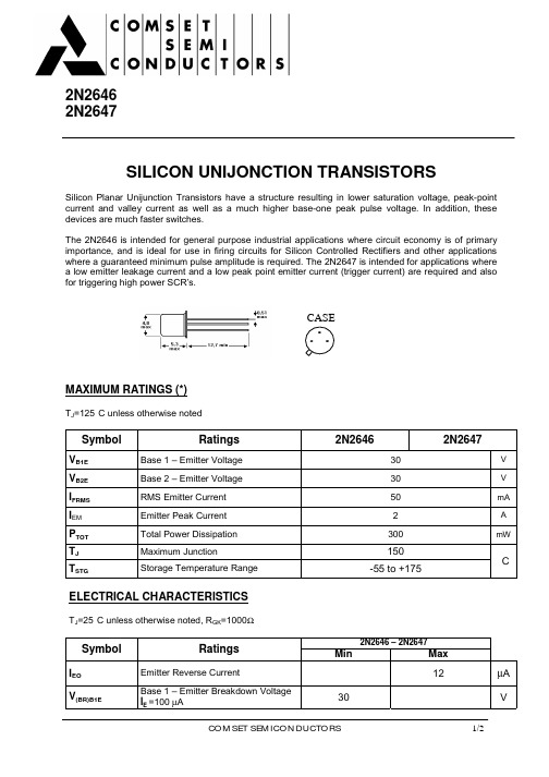
2N26462N2647SILICON UNIJONCTION TRANSISTORSSilicon Planar Unijunction Transistors have a structure resulting in lower saturation voltage, peak-point current and valley current as well as a much higher base-one peak pulse voltage. In addition, these devices are much faster switches.The 2N2646 is intended for general purpose industrial applications where circuit economy is of primary importance, and is ideal for use in firing circuits for Silicon Controlled Rectifiers and other applications where a guaranteed minimum pulse amplitude is required. The 2N2647 is intended for applications where a low emitter leakage current and a low peak point emitter current (trigger current) are required and also for triggering high power SCR’s.MAXIMUM RATINGS (*)T J =125°C unless otherwise notedSymbolRatings2N26462N2647V B1E Base 1 – Emitter Voltage 30V V B2E Base 2 – Emitter Voltage 30V I FRMS RMS Emitter Current 50mA I EM Emitter Peak Current 2A P TOT Total Power Dissipation 300mWT J Maximum Junction150T STGStorage Temperature Range-55 to +175°CELECTRICAL CHARACTERISTICST J =25°C unless otherwise noted, R GK =1000Ω2N2646 – 2N2647SymbolRatingsMin Max I EO Emitter Reverse Current12µA V (BR)B1EBase 1 – Emitter Breakdown Voltage I E =100 µA30VCASE2N26462N26472N2646 – 2N2647 Symbol Ratings Min MaxR BBO Interbase ResistanceV B1B2 = 3 V 4.79.1kΩ2N26460.560.75ηIntrinsic stand-off ratioV B1B2 = 10 V2N26470.680.82-V E(SAT)Emitter Saturation VoltageI E = 50 mA, V B1B2 = 10 V- 2.5V2N26464-I V Valley CurrentV B1B2 = 20 V2N26478-mA2N2646-5I P Peak CurrentV B1B2 = 25 V2N2647-2µA* V DRM or V RSM can be applied for all types on a continuous dc basis without incurring damage.Information furnished is believed to be accurate and reliable. However, CS assumes no responsability for the consequences of use of such information nor for errors that could appear.Data are subject to change without notice.。
at24c256中文手册
精心整理AT24C256中文资料2009-11-15 09:43特性???? 与1MHz I2C 总线兼容64 字节页写缓冲器该器件通过I2C 总线接口进行操作管脚描述管脚名称功能A0 A1 地址输入SDA 串行数据/地址SCL 串行时钟WP 写保护Vcc +1.8V 6.0V 电源功能描述CAT24WC256 支持I2C 总线数据传送协议I2C 总线协议规定任何将数据传送到总线的器件作为发送器任何从总线接收数据的器件为接收器数据传送是由产生串行时钟和所有起始停止信号的主器件控制的CAT24WC256 是作为从器件被操作的主器件和从器件都可以作为发送器或接收器但由主器件控制传送数据发送或接收的模式管脚描述SCL 串行时钟件参阅器件寻址当这些引脚没有连接时其默认值为0I2C 总线协议I2C 总线协议定义如下1 只有在总线空闲时才允许启动数据传送2 在数据传送过程中当时钟线为高电平时数据线必须保持稳定状态不允许有跳变时钟线为高电平时数据线的任何电平变化将被看作总线的起始或停止信号起始信号时钟线保持高电平期间数据线电平从高到低的跳变作为I2C 总线的起始信号SDA 线CAT24WC256 再根据读写控制位R/W 的状态进行读或写操作应答信号I2C 总线数据传送时每成功地传送一个字节数据后接收器都必须产生一个应答信号应答的器件在第9 个时钟周期时将SDA 线拉低表示其已收到一个8 位数据CAT24WC256 在接收到起始信号和从器件地址之后响应一个应答信号如果器件已选择了写操作则在每接收一个8 位字节之后响应一个应答信号止信号后开始内部数据的擦写在内部擦写过程中CAT24WC256 不再应答主器件的任何请求页写在页写模式下单个写周期内CAT24WC256 最多可以写入64 个字节数据页写操作的启动和字节写一样不同在于传送了一字节数据后主器件允许继续发送63 个字节每发送一个字节后CAT24WC256 将响应一个应答位且内部低6 位地址加1 高位地址保持不变如果主器件在发送停止写保护写保护操作特性可使用户避免由于不当操作而造成对存储区域内部数据的改写当WP 管脚接高时整个寄存器区全部被保护起来而变为只可读取CAT24WC256 可以接收从器件地址和字节地址但是装置在接收到第一个数据字节后不发送应答信号从而避免寄存器区域被编程改写读操作CAT24WC256 读操作的初始化方式和写操作时一样仅把R/W 位置为1 有三种不送起始信号从器件地址和它想读取的字节数据的地址执行一个伪写操作在CAT24WC256 应答之后主器件重新发送起始信号和从器件地址此时R/W 位置1 CAT24WC256 响应并发送应答信号然后输出所要求的一个8 位字节数据主器件不发送应答信号但产生一个停止信号连续读连续读操作可通过立即读或选择性读操作启动在CAT24WC256 发送完一个8 位字节数据后主器件产生一个应答信号来响应告知CAT24WC256 主器件要求更多的数据对应每个主机产生的应答信号CAT24WC256 将发送一个8 位数据。
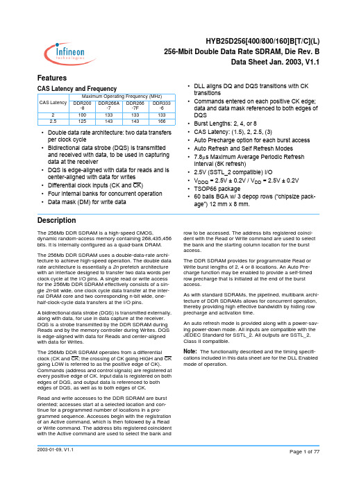
HYB25D256160BTL-7F资料
HYB25D256[400/800/160]B[T/C](L)256-Mbit Double Data Rate SDRAM, Die Rev. BData Sheet Jan. 2003, V1.1Features•Double data rate architecture: two data transfers per clock cycle•Bidirectional data strobe (DQS) is transmitted and received with data, to be used in capturing data at the receiver•DQS is edge-aligned with data for reads and is center-aligned with data for writes •Differential clock inputs (CK and CK)•Four internal banks for concurrent operation •Data mask (DM) for write data •DLL aligns DQ and DQS transitions with CK transitions•Commands entered on each positive CK edge;data and data mask referenced to both edges of DQS•Burst Lengths: 2, 4, or 8•CAS Latency: (1.5), 2, 2.5, (3)•Auto Precharge option for each burst access •Auto Refresh and Self Refresh Modes•7.8m s Maximum Average Periodic Refresh Interval (8K refresh)• 2.5V (SSTL_2 compatible) I/O•V DDQ = 2.5V ± 0.2V / V DD = 2.5V ± 0.2V •TSOP66 package•60 balls BGA w/ 3 depop rows (“chipsize pack-age”) 12 mm x 8 mm.DescriptionThe 256Mb DDR SDRAM is a high-speed CMOS, dynamic random-access memory containing 268,435,456 bits. It is internally configured as a quad-bank DRAM.The 256Mb DDR SDRAM uses a double-data-rate archi-tecture to achieve high-speed operation. The double data rate architecture is essentially a 2n prefetch architecture with an interface designed to transfer two data words per clock cycle at the I/O pins. A single read or write access for the 256Mb DDR SDRAM effectively consists of a sin-gle 2n-bit wide, one clock cycle data transfer at the inter-nal DRAM core and two corresponding n-bit wide, one-half-clock-cycle data transfers at the I/O pins.A bidirectional data strobe (DQS) is transmitted externally, along with data, for use in data capture at the receiver. DQS is a strobe transmitted by the DDR SDRAM during Reads and by the memory controller during Writes. DQS is edge-aligned with data for Reads and center-aligned with data for Writes.The 256Mb DDR SDRAM operates from a differential going LOW is referred to as the positive edge of CK). Commands (address and control signals) are registered at every positive edge of CK. Input data is registered on both edges of DQS, and output data is referenced to both edges of DQS, as well as to both edges of CK.Read and write accesses to the DDR SDRAM are burst oriented; accesses start at a selected location and con-tinue for a programmed number of locations in a pro-grammed sequence. Accesses begin with the registration of an Active command, which is then followed by a Read or Write command. The address bits registered coincident with the Active command are used to select the bank and row to be accessed. The address bits registered coinci-dent with the Read or Write command are used to select the bank and the starting column location for the burst access.The DDR SDRAM provides for programmable Read or Write burst lengths of 2, 4 or 8 locations. An Auto Pre-charge function may be enabled to provide a self-timed row precharge that is initiated at the end of the burst access.As with standard SDRAMs, the pipelined, multibank archi-tecture of DDR SDRAMs allows for concurrent operation, thereby providing high effective bandwidth by hiding row precharge and activation time.An auto refresh mode is provided along with a power-sav-ing power-down mode. All inputs are compatible with the JEDEC Standard for SSTL_2. All outputs are SSTL_2, Class II compatible.Note: The functionality described and the timing specifi-cations included in this data sheet are for the DLL Enabled mode of operation.CAS Latency and FrequencyCAS LatencyMaximum Operating Frequency (MHz) DDR200-8DDR266A-7DDR266-7FDDR333-62100133133133 2.5125143143166Ordering InformationPart Number aa. HYB: designator for memory components25D: DDR-I SDRAMs at Vddq=2.5V 256: 256Mb density400/800/160: Product variations x4, x8 and x16B: Die revision BC/T: Package type FBGA and TSOPL: Low power version (optional) - these components are specifically selected for low IDD6 Self Refresh currents -5/6/7/7F/8: speed grade - see tableOrg.CAS-RCD-RP Latencies Clock (MHz)CAS-RCD-RP Latencies Clock (MHz)Speed Package HYB25D256400BT(L)-6x4 2.5-3-31662-3-3133DDR33366 Pin P-TSOP-IIHYB25D256800BT(L)-6x8HYB25D256160BT(L)-6x16HYB25D256400BT(L)-7x4143DDR266AHYB25D256800BT(L)-7x8HYB25D256160BT(L)-7x16HYB25D256400BT(L)-7F x42-2-2DDR266HYB25D256800BT(L)-7F x8HYB25D256160BT(L)-7F x16HYB25D256400BT(L)-8x4125100DDR200HYB25D256800BT(L)-8x8HYB25D256160BT(L)-8x16HYB25D256400BC(L)-6x4 2.5-3-31662-3-3133DDR33360 Balls P-FBGAHYB25D256800BC(L)-6x8HYB25D256160BC(L)-6x16HYB25D256400BC(L)-7x4143DDR266AHYB25D256800BC(L)-7x8HYB25D256160BC(L)-7x16HYB25D256400BC(L)-7F x42-2-2DDR266HYB25D256800BC(L)-7F x8HYB25D256160BC(L)-7F x16HYB25D256400BC(L)-8x4125100DDR200HYB25D256800BC(L)-8x8HYB25D256160BC(L)-8x16Pin Configuration (TSOP66)123456910111213147815161718192021226665646362615857565554536059525150494847464523242544434226274140282930313233393837363534V DD DQ0V DDQNC DQ1V SSQV DDQNC DQ3V SSQNC NC NC DQ2V DDQNC NC V DD NC NC WE CAS RAS CS NC BA0BA1V SS DQ7V SSQ NC DQ6V DDQ V SSQ NC DQ4V DDQ NC NC NC DQ5V SSQ DQS NC V REF V SS DM CK CK CKE NC A12A11A9V DD NC V DDQNC DQ0V SSQV DDQNC DQ1V SSQNC NC NC NC V DDQNC NC V DD NC NC WE CAS RAS CS NC BA0BA1V SS NC V SSQ NC DQ3V DDQ V SSQ NC DQ2V DDQ NC NC NC NC V SSQ DQS NC V REF V SS DM CK CK CKE NC A12A11A9A10/APA0A1A2A3V DDA10/APA0A1A2A3V DDA8A7A6A5A4V SSA8A7A6A5A4V SS64Mb x 432Mb x 8V DD DQ0V DDQ DQ1DQ2V SSQ V DDQ DQ5DQ6V SSQ DQ7NC DQ3DQ4V DDQ LDQS NC V DD NC LDM WE CAS RAS CS NC BA0BA1A10/APA0A1A2A3V DD16Mb x 16V SS DQ15V SSQ DQ14DQ13V DDQ V SSQ DQ10DQ9V DDQ DQ8NC DQ12DQ11V SSQ UDQS NC V REF V SS UDM CK CK CKE NC A12A11A9A8A7A6A5A4V SSPin Configuration (FBGA)123789123789 VSSQ NC VSS A VDD NC VDDQ VSSQ DQ7VSS A VDD DQ0VDDQ NC VDDQ DQ3B DQ0VSSQ NC NC VDDQ DQ6B DQ1VSSQ NC NC VSSQ NC C NC VDDQ NC NC VSSQ DQ5C DQ2VDDQ NC NC VDDQ DQ2D DQ1VSSQ NC NC VDDQ DQ4D DQ3VSSQ NC NC VSSQ DQS E NC VDDQ NC NC VSSQ DQS E NC VDDQ NC VREF VSS DM F NC VDD NC VREF VSS DM F NC VDD NC CLK CLK G WE CAS CLK CLK G WE CASA12CKE H RAS CS A12CKE H RAS CSA11A9J BA1BA0A11A9J BA1BA0A8A7K A0A10/AP A8A7K A0A10/APA6A5L A2A1A6A5L A2A1A4VSS M VDD A3A4VSS M VDD A3( x 4 )( x8 )Top View (see the balls through the package)123789VSSQ DQ15VSS A VDD DQ0VDDQDQ14VDDQ DQ13B DQ2VSSQ DQ1DQ12VSSQ DQ11C DQ4VDDQ DQ3DQ10VDDQ DQ9D DQ6VSSQ DQ5DQ8VSSQ UDQS E LDQS VDDQ DQ7VREF VSS UDM F LDM VDD NCCLK CLK G WE CASA12CKE H RAS CSA11A9J BA1BA0A8A7K A0A10/APA6A5L A2A1A4VSS M VDD A3( x 16 )Input/Output Functional DescriptionSymbol Type FunctionCK, CK Input Clock:CK and CK are differential clock inputs. All address and control input signals are sam-pled on the crossing of the positive edge of CK and negative edge of CK. Output (read) data is referenced to the crossings of CK and CK (both directions of crossing).CKE Input Clock Enable: CKE HIGH activates, and CKE Low deactivates, internal clock signals and device input buffers and output drivers. Taking CKE Low provides Precharge Power-Down and Self Refresh operation (all banks idle), or Active Power-Down (row Active in any bank). CKE is synchronous for power down entry and exit, and for self refresh entry. CKE is asyn-chronous for self refresh exit. CKE must be maintained high throughout read and write accesses. Input buffers, excluding CK, CK and CKE are disabled during power-down. Input buffers, excluding CKE, are disabled during self refresh.CS Input Chip Select: All commands are masked when CS is registered HIGH. CS provides for exter-nal bank selection on systems with multiple banks. CS is considered part of the command code. The standard pinout includes one CS pin.RAS, CAS, WE Input Command Inputs: RAS, CAS and WE (along with CS) define the command being entered.DM Input Input Data Mask: DM is an input mask signal for write data. Input data is masked when DM is sampled HIGH coincident with that input data during a Write access. DM is sampled on both edges of DQS. Although DM pins are input only, the DM loading matches the DQ and DQS loading.BA0, BA1Input Bank Address Inputs: BA0 and BA1 define to which bank an Active, Read, Write or Pre-charge command is being applied. BA0 and BA1 also determines if the mode register or extended mode register is to be accessed during a MRS or EMRS cycle.A0 - A12Input Address Inputs: Provide the row address for Active commands, and the column address and Auto Precharge bit for Read/Write commands, to select one location out of the memory array in the respective bank. A10 is sampled during a Precharge command to determine whether the Precharge applies to one bank (A10 LOW) or all banks (A10 HIGH). If only one bank is to be precharged, the bank is selected by BA0, BA1. The address inputs also provide the op-code during a Mode Register Set command.DQ Input/Output Data Input/Output: Data bus.DQS Input/Output Data Strobe: Output with read data, input with write data. Edge-aligned with read data, cen-tered in write data. Used to capture write data.NC No Connect: No internal electrical connection is present. V DDQ Supply DQ Power Supply: 2.5V ± 0.2V.V SSQ Supply DQ GroundV DD Supply Power Supply: 2.5V ± 0.2V.V SS Supply GroundV REF Supply SSTL_2 reference voltage: (V DDQ / 2)Block Diagram (64Mb x 4)Block Diagram (32Mb x 8)Functional DescriptionThe 256Mb DDR SDRAM is a high-speed CMOS, dynamic random-access memory containing 268, 435, 456 bits. The 256Mb DDR SDRAM is internally configured as a quad-bank DRAM.The 256Mb DDR SDRAM uses a double-data-rate architecture to achieve high-speed operation. The double-data-rate architecture is essentially a 2n prefetch architecture, with an interface designed to transfer two data words per clock cycle at the I/O pins. A single read or write access for the 256Mb DDR SDRAM consists of a single 2n-bit wide, one clock cycle data transfer at the internal DRAM core and two corresponding n-bit wide, one-half clock cycle data transfers at the I/O pins.Read and write accesses to the DDR SDRAM are burst oriented; accesses start at a selected location and continue for a programmed number of locations in a programmed sequence. Accesses begin with the regis-tration of an Active command, which is then followed by a Read or Write command. The address bits regis-tered coincident with the Active command are used to select the bank and row to be accessed (BA0, BA1 select the bank; A0-A12 select the row). The address bits registered coincident with the Read or Write com-mand are used to select the starting column location for the burst access.Prior to normal operation, the DDR SDRAM must be initialized. The following sections provide detailed infor-mation covering device initialization, register definition, command descriptions and device operation. InitializationDDR SDRAMs must be powered up and initialized in a predefined manner. Operational procedures other than those specified may result in undefined operation. The following criteria must be met: No power sequencing is specified during power up or power down given the following criteria:V DD and V DDQ are driven from a single power converter output ANDV TT meets the specification ANDV REF tracks V DDQ/2orThe following relationship must be followed:V DDQ is driven after or with V DD such that V DDQ < V DD + 0.3 VV TT is driven after or with V DDQ such that V TT < V DDQ + 0.3VV REF is driven after or with V DDQ such that V REF < V DDQ + 0.3VThe DQ and DQS outputs are in the High-Z state, where they remain until driven in normal operation (by a read access). After all power supply and reference voltages are stable, and the clock is stable, the DDR SDRAM requires a 200m s delay prior to applying an executable command.Once the 200m s delay has been satisfied, a Deselect or NOP command should be applied, and CKE should be brought HIGH. Following the NOP command, a Precharge ALL command should be applied. Next a Mode Register Set command should be issued for the Extended Mode Register, to enable the DLL, then a Mode Register Set command should be issued for the Mode Register, to reset the DLL, and to program the operat-ing parameters. 200 clock cycles are required between the DLL reset and any executable command. During the 200 cycles of clock for DLL locking, a Deselect or NOP command must be applied. After the 200 clock cycles, a Precharge ALL command should be applied, placing the device in the “all banks idle” state.Once in the idle state, two AUTO REFRESH cycles must be performed. Additionally, a Mode Register Set command for the Mode Register, with the reset DLL bit deactivated (i.e. to program operating parameters without resetting the DLL) must be performed. Following these cycles, the DDR SDRAM is ready for normal operation.Register DefinitionMode RegisterThe Mode Register is used to define the specific mode of operation of the DDR SDRAM. This definition includes the selection of a burst length, a burst type, a CAS latency, and an operating mode. The Mode Reg-ister is programmed via the Mode Register Set command (with BA0 = 0 and BA1 = 0) and retains the stored information until it is programmed again or the device loses power (except for bit A8, which is self-clearing).Mode Register bits A0-A2 specify the burst length, A3 specifies the type of burst (sequential or interleaved), A4-A6 specify the CAS latency, and A7-A12 specify the operating mode.The Mode Register must be loaded when all banks are idle, and the controller must wait the specified time before initiating the subsequent operation. Violating either of these requirements results in unspecified opera-tion.Burst LengthRead and write accesses to the DDR SDRAM are burst oriented, with the burst length being programmable. The burst length determines the maximum number of column locations that can be accessed for a given Read or Write command. Burst lengths of 2, 4, or 8 locations are available for both the sequential and the interleaved burst types.Reserved states should not be used, as unknown operation or incompatibility with future versions may result.When a Read or Write command is issued, a block of columns equal to the burst length is effectively selected. All accesses for that burst take place within this block, meaning that the burst wraps within the block if a boundary is reached. The block is uniquely selected by A1-Ai when the burst length is set to two, by A2-Ai when the burst length is set to four and by A3-Ai when the burst length is set to eight (where Ai is the most significant column address bit for a given configuration). The remaining (least significant) address bit(s) is (are) used to select the starting location within the block. The programmed burst length applies to both Read and Write bursts.Mode Register OperationA8A7A6A5A4CAS Latency A3A2A1A0Burst LengthBTAddress Bus CAS LatencyA6A5A4Latency 000Reserved 001Reserved0102011 3 (optional)100Reserved 101 1.5 (optional)110 2.5111ReservedBurst LengthA2A1A0Burst Length 000Reserved001201040118100Reserved 101Reserved 110Reserved 111ReservedBA1BA0A11A10A90*0*Mode RegisterOperating Mode* BA0 and BA1 must be 0, 0 to select the Mode Register(vs. the Extended Mode Register).A12 - A9A8A7A6 - A0Operating Mode 000Valid Normal operation Do not reset DLL 010ValidNormal operation in DLL Reset1Reserved ---ReservedA3Burst Type 0Sequential 1InterleaveA12Notes:1.For a burst length of two, A1-Ai selects the two-data-element block; A0 selects the first access within the block.2.For a burst length of four, A2-Ai selects the four-data-element block; A0-A1 selects the first access within the block.3.For a burst length of eight, A3-Ai selects the eight-data- element block; A0-A2 selects the first access within the block.4.Whenever a boundary of the block is reached within a given sequence above, the following access wraps within the block.Burst TypeAccesses within a given burst may be programmed to be either sequential or interleaved; this is referred to as the burst type and is selected via bit A3. The ordering of accesses within a burst is determined by the burst length, the burst type and the starting column address, as shown in Burst Definition on page 12.Read LatencyThe Read latency, or CAS latency, is the delay, in clock cycles, between the registration of a Read command and the availability of the first burst of output data. The latency can be programmed 2, 2.5 or 3 clocks. CAS latency of 1.5 is an optional feature on this device.If a Read command is registered at clock edge n, and the latency is m clocks, the data is available nominally coincident with clock edge n + m.Reserved states should not be used as unknown operation or incompatibility with future versions may result.Burst DefinitionBurst LengthStarting Column AddressOrder of Accesses Within a BurstA2A1A0Type = SequentialT ype = Interleaved20-10-111-01-04000-1-2-30-1-2-3011-2-3-01-0-3-2102-3-0-12-3-0-1113-0-1-23-2-1-080000-1-2-3-4-5-6-70-1-2-3-4-5-6-70011-2-3-4-5-6-7-01-0-3-2-5-4-7-60102-3-4-5-6-7-0-12-3-0-1-6-7-4-50113-4-5-6-7-0-1-23-2-1-0-7-6-5-41004-5-6-7-0-1-2-34-5-6-7-0-1-2-31015-6-7-0-1-2-3-45-4-7-6-1-0-3-21106-7-0-1-2-3-4-56-7-4-5-2-3-0-11117-0-1-2-3-4-5-67-6-5-4-3-2-1-0Operating ModeThe normal operating mode is selected by issuing a Mode Register Set Command with bits A7-A12 set to zero, and bits A0-A6 set to the desired values. A DLL reset is initiated by issuing a Mode Register Set com-mand with bits A7 and A9-A12 each set to zero, bit A8 set to one, and bits A0-A6 set to the desired values. A Mode Register Set command issued to reset the DLL should always be followed by a Mode Register Set command to select normal operating mode.All other combinations of values for A7-A12 are reserved for future use and/or test modes. Test modes and reserved states should not be used as unknown operation or incompatibility with future versions may result. Required CAS LatenciesExtended Mode RegisterThe Extended Mode Register controls functions beyond those controlled by the Mode Register; these addi-tional functions include DLL enable/disable, and output drive strength selection (optional). These functions are controlled via the bits shown in the Extended Mode Register Definition. The Extended Mode Register is programmed via the Mode Register Set command (with BA0 = 1 and BA1 = 0) and retains the stored informa-tion until it is programmed again or the device loses power. The Extended Mode Register must be loaded when all banks are idle, and the controller must wait the specified time before initiating any subsequent oper-ation. Violating either of these requirements result in unspecified operation.DLL Enable/DisableThe DLL must be enabled for normal operation. DLL enable is required during power up initialization, and upon returning to normal operation after having disabled the DLL for the purpose of debug or evaluation. The DLL is automatically disabled when entering self refresh operation and is automatically re-enabled upon exit of self refresh operation. Any time the DLL is enabled, 200 clock cycles must occur before a Read command can be issued. This is the reason 200 clock cycles must occur before issuing a Read or Write command upon exit of self refresh operation.Output Drive StrengthThe normal drive strength for all outputs is specified to be SSTL_2, Class II. In addition this design version supports a weak driver mode for lighter load and/or point-to-point environments which can be activated during mode register set. I-V curves for the normal and weak drive strength are included in this document.Extended Mode Register DefinitionA 8A 7A 6A 5A 4A 3A 2A 1A 0Address Bus Drive StrengthA 1Drive Strength0Normal 1WeakBA1BA0Operating ModeA 11A 10A 90*1** BA0 and BA1 must be 1, 0 to select the Extended Mode Register Mode RegisterExtendedDSDLLA 0DLL 0Enable 1DisableAn - A3A2 - A0Operating Mode 0ValidNormal Operation --All other states Reserved(vs. the base Mode Register)A 12A 20must be set to 0CommandsCommandsDeselectThe Deselect function prevents new commands from being executed by the DDR SDRAM. The DDR SDRAM is effectively deselected. Operations already in progress are not affected.No Operation (NOP)The No Operation (NOP) command is used to perform a NOP to a DDR SDRAM. This prevents unwanted commands from being registered during idle or wait states. Operations already in progress are not affected. Mode Register SetThe mode registers are loaded via inputs A0-A12, BA0 and BA1. See mode register descriptions in the Reg-ister Definition section. The Mode Register Set command can only be issued when all banks are idle and no bursts are in progress. A subsequent executable command cannot be issued until t MRD is met.ActiveThe Active command is used to open (or activate) a row in a particular bank for a subsequent access. The value on the BA0, BA1 inputs selects the bank, and the address provided on inputs A0-A12 selects the row. This row remains active (or open) for accesses until a Precharge (or Read or Write with Auto Precharge) is issued to that bank. A Precharge (or Read or Write with Auto Precharge) command must be issued and com-pleted before opening a different row in the same bank.ReadThe Read command is used to initiate a burst read access to an active (open) row. The value on the BA0, BA1 inputs selects the bank, and the address provided on inputs A0-Ai, Aj (where [i = 8, j = don’t care] forx16, [i = 9, j = don’t care] for x8 and [i = 9, j = 11] for x4) selects the starting column location. The value on input A10 determines whether or not Auto Precharge is used. If Auto Precharge is selected, the row being accessed is precharged at the end of the Read burst; if Auto Precharge is not selected, the row remains open for subsequent accesses.WriteThe Write command is used to initiate a burst write access to an active (open) row. The value on the BA0, BA1 inputs selects the bank, and the address provided on inputs A0-Ai, Aj (where [i = 9, j = don’t care] for x8; where [i = 9, j = 11] for x4) selects the starting column location. The value on input A10 determines whether or not Auto Precharge is used. If Auto Precharge is selected, the row being accessed is precharged at the end of the Write burst; if Auto Precharge is not selected, the row remains open for subsequent accesses. Input data appearing on the DQs is written to the memory array subject to the DM input logic level appearing coin-cident with the data. If a given DM signal is registered low, the corresponding data is written to memory; if the DM signal is registered high, the corresponding data inputs are ignored, and a Write is not executed to that byte/column location.PrechargeThe Precharge command is used to deactivate (close) the open row in a particular bank or the open row(s) in all banks. The bank(s) will be available for a subsequent row access a specified time (t RP) after the Precharge command is issued. Input A10 determines whether one or all banks are to be precharged, and in the case where only one bank is to be precharged, inputs BA0, BA1 select the bank. Otherwise BA0, BA1 are treated as “Don’t Care.” Once a bank has been precharged, it is in the idle state and must be activated prior to anyRead or Write commands being issued to that bank. A precharge command is treated as a NOP if there is no open row in that bank, or if the previously open row is already in the process of precharging.Auto PrechargeAuto Precharge is a feature which performs the same individual-bank precharge functions described above, but without requiring an explicit command. This is accomplished by using A10 to enable Auto Precharge in conjunction with a specific Read or Write command. A precharge of the bank/row that is addressed with the Read or Write command is automatically performed upon completion of the Read or Write burst. Auto Pre-charge is nonpersistent in that it is either enabled or disabled for each individual Read or Write command. Auto Precharge ensures that the precharge is initiated at the earliest valid stage within a burst. The user must not issue another command to the same bank until the precharge (t RP) is completed. This is determined as if an explicit Precharge command was issued at the earliest possible time, as described for each burst type in the Operation section of this data sheet.Burst TerminateThe Burst Terminate command is used to truncate read bursts (with Auto Precharge disabled). The most re-cently registered Read command prior to the Burst Terminate command is truncated, as shown in the Opera-tion section of this data sheet.Auto RefreshAuto Refresh is used during normal operation of the DDR SDRAM and is analogous to CAS Before RAS (CBR) Refresh in previous DRAM types. This command is nonpersistent, so it must be issued each time a refresh is required.The refresh addressing is generated by the internal refresh controller. This makes the address bits “Don’t Care” during an Auto Refresh command. The 256Mb DDR SDRAM requires Auto Refresh cycles at an aver-age periodic interval of 7.8 m s (maximum).To allow for improved efficiency in scheduling and switching between tasks, some flexibility in the absolute refresh interval is provided. A maximum of eight Auto Refresh commands can be posted in the system, meaning that the maximum absolute interval between any Auto Refresh command and the next Auto Refresh command is 9 * 7.8 m s (70.2m s). This maximum absolute interval is short enough to allow for DLL updates internal to the DDR SDRAM to be restricted to Auto Refresh cycles, without allowing too much drift in t AC between updates.Self RefreshThe Self Refresh command can be used to retain data in the DDR SDRAM, even if the rest of the system is powered down. When in the self refresh mode, the DDR SDRAM retains data without external clocking. The Self Refresh command is initiated as an Auto Refresh command coincident with CKE transitioning low. The DLL is automatically disabled upon entering Self Refresh, and is automatically enabled upon exiting Self Refresh (200 clock cycles must then occur before a Read command can be issued). Input signals except CKE (low) are “Don’t Care” during Self Refresh operation.CKE returning high. Once CKE is high, the SDRAM must have NOP commands issued for t XSNR because time is required for the completion of any internal refresh in progress. A simple algorithm for meeting both refresh and DLL requirements is to apply NOPs for 200 clock cycles before applying any other command.Truth Table 1a: CommandsName (Function)CS RAS CAS WE Address MNE Notes Deselect (Nop)H X X X X NOP1, 9 No Operation (Nop)L H H H X NOP1, 9 Active (Select Bank And Activate Row)L L H H Bank/Row ACT1, 3 Read (Select Bank And Column, And Start Read Burst)L H L H Bank/Col Read1, 4 Write (Select Bank And Column, And Start Write Burst)L H L L Bank/Col Write1, 4 Burst Terminate L H H L X BST1, 8 Precharge (Deactivate Row In Bank Or Banks)L L H L Code PRE1, 5 Auto Refresh Or Self Refresh (Enter Self Refresh Mode)L L L H X AR / SR1, 6, 7 Mode Register Set L L L L Op-Code MRS1, 21.CKE is HIGH for all commands shown except Self Refresh.2.BA0, BA1 select either the Base or the Extended Mode Register (BA0 = 0, BA1 = 0 selects Mode Register; BA0 = 1, BA1 = 0selects Extended Mode Register; other combinations of BA0-BA1 are reserved; A0-A12 provide the op-code to be written to the selected Mode Register.)3.BA0-BA1 provide bank address and A0-A12 provide row address.4.BA0, BA1 provide bank address; A0-A i provide column address (where i = 8for x16, i = 9 for x8 and 9, 11 for x4); A10 HIGHenables the Auto Precharge feature (nonpersistent), A10 LOW disables the Auto Precharge feature.5.A10 LOW: BA0, BA1 determine which bank is precharged.A10 HIGH: all banks are precharged and BA0, BA1 are “Don’t Care.”6.This command is AUTO REFRESH if CKE is HIGH; Self Refresh if CKE is LOW.7.Internal refresh counter controls row and bank addressing; all inputs and I/Os are “Don’t Care” except for CKE.8.Applies only to read bursts with Auto Precharge disabled; this command is undefined (and should not be used) for read bursts withAuto Precharge enabled or for write bursts9.Deselect and NOP are functionally interchangeable.Truth Table 1b: DM OperationName (Function)DM DQs NotesWrite Enable L Valid1Write Inhibit H X1ed to mask write data; provided coincident with the corresponding data.。
NTE2586资料
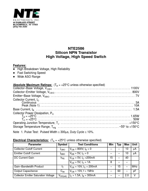
NTE2586 Silicon NPN Transistor High Voltage, High Speed Switch
Features: D High Breakdown Voltage, High Reliability D Fast Switching Speed D Wide ASO Range Absolute Maximum Ratings: (TA = +25°C unless otherwise specified) Collector–Base Voltage, VCBO . . . . . . . . . . . . . . . . . . . . . . . . . . . . . . . . . . . . . . . . . . . . . . . . . . . . . 1100V Collector–Emitter Voltage, VCEO . . . . . . . . . . . . . . . . . . . . . . . . . . . . . . . . . . . . . . . . . . . . . . . . . . . . . 800V Emitter–Base Voltage, VEBO . . . . . . . . . . . . . . . . . . . . . . . . . . . . . . . . . . . . . . . . . . . . . . . . . . . . . . . . . . 7V Collector Current, IC Continuous . . . . . . . . . . . . . . . . . . . . . . . . . . . . . . . . . . . . . . . . . . . . . . . . . . . . . . . . . . . . . . . . . . . 3A Peak (Note 1) . . . . . . . . . . . . . . . . . . . . . . . . . . . . . . . . . . . . . . . . . . . . . . . . . . . . . . . . . . . . . . . . 10A Base Current, IB . . . . . . . . . . . . . . . . . . . . . . . . . . . . . . . . . . . . . . . . . . . . . . . . . . . . . . . . . . . . . . . . . . 1.5A Collector Power Dissipation, PC TA = +25°C . . . . . . . . . . . . . . . . . . . . . . . . . . . . . . . . . . . . . . . . . . . . . . . . . . . . . . . . . . . . . . . . 1.65W TC = +25°C . . . . . . . . . . . . . . . . . . . . . . . . . . . . . . . . . . . . . . . . . . . . . . . . . . . . . . . . . . . . . . . . . 50W Operating Junction Temperature, TJ . . . . . . . . . . . . . . . . . . . . . . . . . . . . . . . . . . . . . . . . . . . . . . . +150°C Storage Temperature Range, Tstg . . . . . . . . . . . . . . . . . . . . . . . . . . . . . . . . . . . . . . . . . . –55° to +150°C Note 1. Pulse Test: Pulsed Width ≤ 300µs, Duty Cycle ≤ 10%. Electrical Characteristics: (TA = +25°C unless otherwise specified)
2586规格书 译文
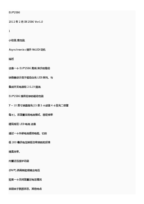
EUP25862012年2月DS2586 Ver1.01小包装,高性能,Asynchronies提升WLED司机描述这是一个EUP2586高频,异步的推动转换器设计用于驱动白光LED阵列。
与集成开关电源和2 0.19限流,EUP2586提供足够的驱动性能7 ~ 10英寸液晶背光(13串3个或者4个发光二极管每个)。
该装臵采用电流模式、固定频率建筑规范LED电流,这是通过一个外部电流感测电阻。
它的低200毫伏电压降低功率损耗和反馈提高效率。
内臵过压保护功能(OVP),西南销监视输出电压如果一个关闭装臵过电压情况目前由于断路状态。
其他特点包括软启动、过电流限制,热保护和低电压闭锁。
这EUP2586是可得到的在小TSOT23-5包裹送到客户提供最佳的解决方案对印刷电路板的空间特征2.6 V输入范围5.5 V内部0.19,18 V MOSFET开关效率高达到93%在表面温度低ILED = 180麻1兆赫开关频率2一个限流导致过电压保护开放内部Soft-StartPWM(脉宽调制)和直流模糊控制可在TSOT23-5包装RoHS认证,并无100%的铅无卤应用7到10英寸液晶面板中部背光Netbook背光便携式媒体播放器GPS导航系统典型应用电路图1。
申请EUP2586 PWM变白光LED驱动EUP25862012年2月DS2586 Ver1.02图2。
框图销配臵包装类型销配臵TSOT23-5销描述销TSOT23-5描述1 SW开关的密码。
这是流失的内部电源开关。
连接电感/二极管在这里。
减少微量区这个别针减少电磁干扰(EMI)。
2电唱机共同点。
连接销到地面的飞机。
3弗拉维奥-布里亚托利反馈的密码。
参考电压是200毫伏。
连接阴极发光二极管(LED)和最低的电阻在这里。
根据计算电阻价值公式:= 200千瓦/ ILED RFB4在芯片使别针。
连接到1.4 V或更高的电压,使装臵,0.3 V或更少电压禁用设备。
5在输入电压。
