L294中文资料
我见过的最好的LM2940 与TL431中文资料
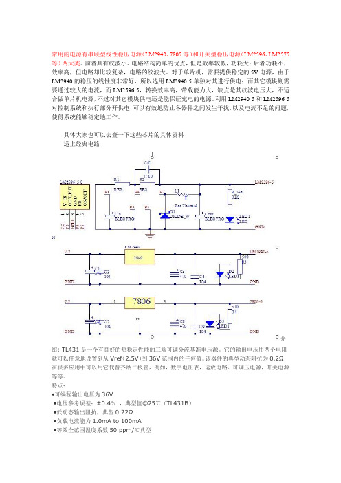
常用的电源有串联型线性稳压电源(LM2940、7805等)和开关型稳压电源(LM2596、LM2575等)两大类。
前者具有纹波小、电路结构简单的优点,但是效率较低,功耗大;后者功耗小,效率高,但电路却比较复杂,电路的纹波大。
对于单片机,需要提供稳定的5V电源,由于LM2940的稳压的线性度非常好,所以选用LM2940-5单独对其进行供电;而其它模块则需要通过较大的电流,而LM2596-5,转换效率高,带载能力大,缺点是其纹波电压大,不适合做单片机电源,不过对其它模块供电还是能保证充电的电源。
利用LM2940-5和LM2596-5对控制系统和执行部分开供电,可以有效地防止各器件之间发生干扰,以及电流不足的问题,使得系统能够稳定地工作。
具体大家也可以去查一下这些芯片的具体资料送上经典电路介绍: TL431是一个有良好的热稳定性能的三端可调分流基准电压源。
它的输出电压用两个电阻就可以任意地设置到从Vref(2.5V)到36V范围内的任何值。
该器件的典型动态阻抗为0.2Ω,在很多应用中可以用它代替齐纳二极管,例如,数字电压表,运放电路、可调压电源,开关电源等等。
特点:•可编程输出电压为36V•电压参考误差:±0.4%,典型值@25℃(TL431B)•低动态输出阻抗,典型0.22Ω•负载电流能力1.0mA to 100mA•等效全范围温度系数50 ppm/℃典型• 温度补偿操作全额定工作温度范围•低输出噪声电压图1 TO92封装引脚图图2 8脚封装引脚功能图3 SOP-8 贴片封装引脚图图4 TL431符号及内部方框图图5 TL431内部电路图MAXIMUM RATINGS (Full operating ambient temperature range applies, unless除非另有说明。
)除非另有说明。
)图6 测试电路VKA = Vref 图7 测试电路VKA > Vref 图8 测试电路for Ioff曲线图:图9 阴极电流与阴极电压图10 阴极电流与阴极电压图11 参考输入电压与常温图12 参考输入电流与常温图13 变化的参考输入电压与阴极电压图14 断态阴极电流随环境温度图15 动态阻抗与频率图16 动态阻抗随环境温度图17 开环电压增益与频率图18 谱噪声密度图19 脉冲响应图20 稳定的边界条件应用法:图21测试电路曲线a 边界条件的稳定性图22曲线测试电路的B,C和D边界条件的稳定性图23并联稳压器电路图图24 大电流并联稳压器电路图25 控制三端固定稳压输出电路图26 串联稳压调节电路图27 过压保护电路图28 恒流源电路图29 恒定流入电流源电路图30 双向可控硅过压保护电路图31 电压监视器电路图32 单电源比较温度补偿电路图33 线性欧姆表电路图图34 简单的400毫瓦唱机放大器电路图35 高效率降压型开关转换器电路图图36 简体TL431器件模型图37 封装图图38 SOP-8 贴片封装图图39 封装图以上文件译自MOTOROLA 公司TL431。
L295;中文规格书,Datasheet资料
where: R1 and R2 are the resistance and inductance of the load and V is the voltage available on the load (Vs Vdrop - Vsense). The current increases until the voltage on the external sensing resistor, RS1, reaches the reference voltage, Vref1. This peak current, Ip1, is given by: V
15
VREF2
October 2003
1/7
/
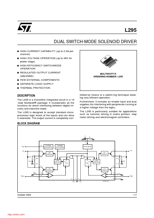
L295
ABSOLUTE MAXIMUM RATINGS
Symbol VS VSS VEN, Vi Vref Io Supply voltage Logic supply voltage Enable and input voltage Reference voltage Peak output current (each channel) - non repetitive (t = 100 µsec) - repetitive (80% on - 20% off; Ton = 10ms) - DC operation Total power dissipation (at Tcase = 75 ″C Storage and junction temperature Parameter Value 50 12 7 7 3 2.5 2 25 - 40 to 150 Unit V V V V A A A W °C
L295中文资料

L295DUAL SWITCH-MODE SOLENOID DRIVERPRELIMINARY DATAHIGH CURRENT CAPABILITY (up to 2.5A per channel)HIGH VOLTAGE OPERATION (up to 46V for power stage)HIGH EFFICIENCY SWITCHMODE OPERATION REGULATED OUTPUT CURRENT (adjustable)FEW EXTERNAL COMPONENTS SEPARATE LOGIC SUPPLY THERMAL PROTECTIONDESCRIPTIONThe L295 is a monolithic integrated circuit in a 15 -lead Multiwatt ® package; it incorporates all the functions for direct interfacing between digital cir-cuitry and inductive loads. The L295 is designed to accept standard microprocessor logic levels at the inputs and can drive 2 solenoids. The output current is completely controlled by means of a switch-March 1993ABSOLUTE MAXIMUM RATINGSing technique allowing very efficient operation.Furthermore, it includes an enable input and dual supplies (for interfacing with peripherals running at a higher voltage than the logic).The L295 is particularly suitable for applications such as hammer driving in matrix printers, stepmotor driving and electromagnet controllers.APPLICATION CIRCUIT1/8CONNECTION DIAGRAM(top view)BLOCK DIAGRAMSymbol ParameterValue Unit R th-j-case Thermal resistance junction-case max 3°C/W R th-j-ambThermal resistance junction-ambientmax35°C/WTHERMAL DATA(*) V drop = V CEsat Q1 + V CEsat Q2.ELECTRICAL CHARACTERISTICS (Refer to the application circuit, V ss = 5V, V s = 36V; T j = 25°C; L =Low; H = High; unless otherwise specified)APPLICATION CIRCUITD2, D4 = 2A High speed diodesD1, D3 = 1A High speed diodesR1 = R2 = 2ΩL1 = L2 = 5 mH)trr ≤ 200 ns FUNCTIONAL DESCRIPTIONThe L295 incorporates two indipendent driver channals with separate inputs and outputs, each capable of driving an inductive load (see block diagram).The device is controlled by three micriprocessor compatible digital inputs and two analog inputs. These inputs are:EN chip enable (digital input, active low), enables both channels when in the lowstate.V in1, V in2channel inputs (digital inputs, active high), enable each channel inde-pendently. A channel is actived whenboth EN and the appropriate channelinput are active.V ref1, V ref2 referce voltages (analog inputs), used to program the peak load currents.Peak load current is proportional to V ref.Since the two channels are identical, only channel one will be described.The following description applies also the channel two, replacing FF2 for FF1, V ref for V ref1 etc. When the channel is avtivated by low level on the EN input and a high level on the channel input, V in2, the output transistors Q1 and Q2 switch on and current flows in the load according to the exponen-tial law:I =VR1( 1 − e− R1 tL1)where:R1 and R2 are the resistance and in-ductance of the load and V is the volt-age available on the load (V s - V drop -V sense).The current increases until the voltage on the ex-ternal sensing resistor, R S1, reaches the reference voltage, V ref1. This peak current, I p1, is given by:I p1=V ref1R S1At this point the comparator output, Vomp1, sete the RS flip-flop, FF1, that turns off the output tran-sistor, Q1. The load current flowing through D2, Q2, R S1, decreases according to the law:I =(V AR1+ I p1) e− R1 tL1−V AR1 where V A = V CEsat Q2 + V sense + V D2If the oscillator pin (9) is connected to ground the load current falls to zero as shown in fig. 1.At this time t2 the channel 1 is disabled, by taking the inputs V in1 low and/or EN high, and the output transistor Q2 is turned off. The load current flows through D2 and D1 according to the law:I =(V BR1+ I T2) e− R1 tL1−V BR1where V B = V S + V D1 + V D2I T2 = current value at the time t2.Fig. 2 in shows the current waveform obtained with an RC network connected between pin 9 and ground. From to t1 the current increases as in fig.1. A difference exists at the time t2 because the current starts to increase again. At this time a pulse is produced by the oscillator circuit that resets the flip.flop, FF1, and switches on the outout transistor, Q1. The current increases until the drop on the sensing resistor R S1 is equal to V ref1 (t3) and the cycle repeats.SIGNAL WAVEFORMS The switching frequency depends on the value R and C, as shown in fig. 4 and must be chosen in the range 10 to 30 KHz.It is possible with external hardware to change the reference voltage V ref in order to obtain a high peak current I p and a lower holding current I h (see fig. 3). The L295 is provided with a thermal protection that switches off all the output transistors when the junction temperature exceeds 150°C. The pres-ence of a hysteresis circuit makes the IC work again aftera fall of the junction temperature of about 20°C.The analog input pins (V ref1 , V ref2) can be left open or connected to V ss; in this case the circuit works with an internal reference voltage of about 2.5V and the peak current in the load is fixed only by the value of R s:I p=2.5RSFigure 1. Load current waveform with pin 9connected to GND.Figure 2. Load current waveform with externalR-C network connected between pin 9 and5/8SIGNAL WAVEFORMS (continued)Figure 3. With V ref changed by hardware.Figure 4. Switching frequency vs. values of Rand C.MULTIWATT15 PACKAGE MECHANICAL DATAInformation furnished is believed to be accurate and reliable. However, SGS-THOMSON Microelectronics assumes no responsibility for the consequences of use of such information nor for any infringement of patents or other rights of third parties which may result from its use. No license is granted by implication or otherwise under any patent or patent rights of SGS-THOMSON Microelectronics. Specifications mentioned in this publication are subject to change without notice. This publication supersedes and replaces all information previously supplied. SGS-THOMSON Microelectronics products are not authorized for use as critical components in life support devices or systems without express written approval of SGS-THOMSON Microelectronics.© 1994 SGS-THOMSON Microelectronics - All Rights ReservedSGS-THOMSON Microelectronics GROUP OF COMPANIESAustralia - Brazil - France - Germany - Hong Kong - Italy - Japan - Korea - Malaysia - Malta - Morocco - The Netherlands - Singapore -Spain - Sweden - Switzerland - T aiwan - Thaliand - United Kingdom - U.S.A.。
LM2940CT中文资料
882243
882244
Top View See NS Package Number J16A TO-263 (S) Surface-Mount Package
Top View See NS Package Number WG16A LLP (LD) 8-Lead
882211
Top View
882212
Ordering Information
Temp Range 0°C Output Voltage 5.0 LM2940CT-5.0 LM2940CS-5.0 LM2940CSX -5.0 8.0 – – – 9.0 LM2940CT-9.0 LM2940CS-9.0 LM2940CSX -9.0 10 – – – 12 LM2940CT-12 LM2940CS-12 LM2940CSX -12 15 LM2940CT-15 LM2940CS-15 LM2940CSX -15 TO-263 Package TO-220
≤ TJ ≤
125°C
For information on military temperature range products, please go to the Mil/Aero Web Site at /appinfo/milaero/index.html.
2
元器件交易网
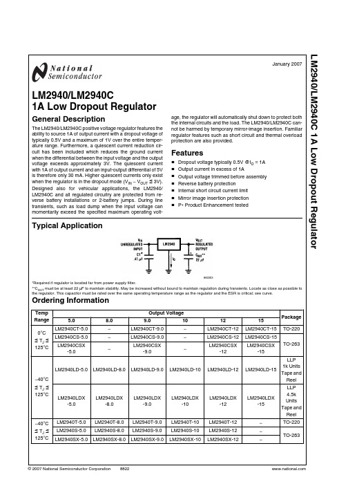
LM2940/LM2940C
Absolute Maximum Ratings (Note 1)
If Military/Aerospace specified devices are required, please contact the National Semiconductor Sales Office/ Distributors for availability and specifications. LM2940S, J, WG, T, MP ≤ 100 ms LM2940CS, T ≤ 1 ms Internal Power Dissipation (Note 2) Maximum Junction Temperature Storage Temperature Range Soldering Temperature (Note 3) TO-220 (T), Wave TO-263 (S) 60V 45V Internally Limited 150°C −65°C ≤ TJ ≤ +150°C 260°C, 10s 235°C, 30s
29400资料
PRELIMINARY
(February, 2001, Version 0.1)
1
AMIC Technology, Inc.
元器件交易Hale Waihona Puke
A29400 Series
The host system can detect whether a program or erase operation is complete by reading the I/O7 ( Data Polling) and I/O6 (toggle) status bits. After a program or erase cycle has been completed, the device is ready to read array data or accept another command. The sector erase architecture allows memory sectors to be erased and reprogrammed without affecting the data contents of other sectors. The A29400 is fully erased when shipped from the factory. The hardware sector protection feature disables operations for both program and erase in any combination of the sectors of memory. This can be achieved via programming equipment. The Erase Suspend feature enables the user to put erase on hold for any period of time to read data from, or program data to, any other sector that is not selected for erasure. True background erase can thus be achieved. Power consumption is greatly reduced when the device is placed in the standby mode. The hardware RESET pin terminates any operation in progress and resets the internal state machine to reading array data.
LM2940IMP中文资料

60V 45V
Internally Limited 150°C
−65°C ≤ TJ ≤ +150°C
260°C, 10s 235°C, 30s
SOT-223 (MP) LLP-8 (LD) ESD Susceptibility (Note 4)
260°C, 30s 235°C, 30s
2 kV
Operating Conditions (Note 1)
LM2940T-8.0 LM2940S-8.0 LM2940SX-8.0
LM2940T-9.0 LM2940S-9.0 LM2940SX-9.0
LM2940T-10 LM2940S-10 LM2940SX-10
12 LM2940CT-12 LM2940CS-12 LM2940CSX
-12
LM2940LD-12
Connection Diagrams
TO-220 (T) Plastic Package
SOT-223 (MP) 3-Lead
882202
Front View See NS Package Number TO3B
16-Lead Dual-in-Line Package (J)
Front View
882242
Range
5.0
8.0
9.0
10
12
Package 15
−40°C
≤ TA ≤
85°C
LM2940IMP-5.0 LM2940IMP-8.0 LM2940IMP-9.0 LM2940Iቤተ መጻሕፍቲ ባይዱP-10
LM2940IMPX LM2940IMPX LM2940IMPX LM2940IMPX
-5.0
一种膨胀阻燃PP体系及其燃烧性能
第25卷第3期高分子材料科学与工程Vol.25,No.3 2009年3月POL YM ER MA TERIAL S SCIENCE AND EN GIN EERIN GMar.2009一种膨胀阻燃PP 体系及其燃烧性能韩俊峰1,王德义1,刘 云1,王玉忠1,2(1.四川大学化学学院,降解与阻燃高分子材料四川省重点实验室,环境友好高分子材料教育部工程研究中心,四川成都610064; 2.高分子材料工程国家重点实验室(四川大学),四川成都610065)摘要:制备了一种阻燃聚丙烯/膨胀阻燃剂(IFR )/蒙脱土(MM T )膨胀阻燃体系,研究了不同阻燃组分含量对体系阻燃性能的影响。
结果表明,阻燃剂总添加量为30%,其中的成炭剂和聚磷酸铵(APP )的配比为1∶2时,体系的极限氧指数为29%,垂直燃烧试验(UL 294)达到V 22级;而在上述体系中添加0.5%的MM T 时,体系的L OI 提高到31%,垂直燃烧试验(UL 294)通过V 20级,表现出较好的协同阻燃效果。
采用扫描电境(SEM )和红外光谱(FT 2IR )对体系的固相残炭进行了观察和分析,探讨了可能的阻燃机理。
关键词:聚丙烯;膨胀阻燃剂;蒙脱土;阻燃性中图分类号:TQ314.24+8 文献标识码:A 文章编号:100027555(2009)0320138204收稿日期:2008210206基金项目:国家杰出青年科学基金(50525309)通讯联系人:王玉忠,主要从事阻燃材料与降解材料等领域的研究,E 2mail :yzwang @ 聚丙烯(PP )是一种产量大、性能优异的通用塑料,具有广泛的用途,并且作为工程塑料的使用范围正在逐渐扩大[1]。
然而,其氧指数仅为17.8%,属于高易燃材料,限制了其应用。
近年来,由于含卤阻燃剂被限制使用,因此PP 的无卤阻燃研究受到了广泛的关注[2],其中无卤膨胀型阻燃剂由于其低烟、低毒、无腐蚀性气体产生等优点而成为研究的热点之一[3]。
IA294中文资料
CHARACTERISTICS
(Typical, @ 25°C, Vs = +15 VDC unless otherwise noted.) GAIN (Non-inverting) ACCURACY Vs. Temperature Nonlinearity Differential Input Impedance Common Mode Input Impedance INPUT VOLTAGE Max. Safe Differential Input Pulse, 10ms Duration Max. Safe Common Mode Input (DC cont.) INPUT BIAS CURRENT Vs. Temperature (0 to + 70°C) SAFETY CURRENT LIMITS INPUT NOISE (5K UNBALANCE) Voltage .05Hz to 100Hz, pp Voltage 10Hz to 1kHz, rms. Current .05Hz to 1kHz, rms. COMMON MODE REJECTION Input to Output, CMV = 115 VAC, 60Hz Balanced Source Impedance 5KΩ Source Imbalance Two Inputs to Input Reference CMV = 10V p-p, 60Hz 5KΩ Source Imbalance OUTPUT Range (50KΩ Load) Output Impedance Max. CMV, Outputs to Power Common Offset Voltage Referred to Input Vs. Temperature (0° to 70°C) Vs. Supply Voltage FREQUENCY RESPONSE Small Signal, - 3 dB Full Power, 6V pp Overload Recovery 10V / V ±2% ±. 01%/°C ±0.1% 3 X 10⁸Ω || 3pF 3 X 10¹⁰Ω || 20pF ±1V min. ±240V rms. ±6500V peak ±5000VDC ±2nA ±0.02nA/°C 10µA max.
2944中文资料
Capable of driving loads to 4 A at supply voltages to 60 V (induc-tive loads to 35 V), the UDN2944W is a quad high-current, high-voltage source driver. Each of the four power drivers can provide space- and cost-saving interface between low-level signal-processing circuits and high-power loads in harsh environments.Individual supply lines have been provided for each pair of drivers so that different supplies can be used to drive multiple loads. The controlling inputs are TTL or CMOS compatible. The outputs include transient-suppression diodes for inductive loads.This quad Darlington array is designed to serve as an interface between low-level circuitry and peripheral-power loads such as sole-noids, motors, incandescent displays, heaters, and similar loads of up to 240 W per channel. The UDN2944W is an ideal complement to the UDN2878W quad 4 A sink driver.For maximum power-handling capability, the UDN2944W driver is supplied in a 12-pin single in-line, power-tab package that allows efficient attachment of an external heat sink for maximum allowable package power dissipation. An external heat sink is usually required for proper operation of this device. The tab is at ground potential and needs no insulation.FEATURESI Output Current to 4 A I Output Voltage to 60 V I Loads to 960 WI Integral Output Suppression Diodes I TTL and CMOS Compatible Inputs I Plastic Single In-Line Package IHeat-Sink Tab2944QUAD HIGH-CURRENT,HIGH-VOLTAGE SOURCE DRIVERABSOLUTE MAXIMUM RATINGS at +25°C Free-Air TemperatureSupply Voltage Range, V S ..... 10 V to 60 V Output Current, I OUT(continuous)............................... -4.0 A (peak)......................................... -5.0 A Input Voltage, V IN ................................ 15 V Package Power Dissipation,P D ....................................... See Graph Operating Temperature Range,T A ................................ -20°C to +85°C Storage Temperature Range,T S .............................. -55°C to +150°C Output current rating will be limited by ambient temperature, duty cycle, heat sinking, air flow, and number of outputsconducting. Under any set of conditions, do not exceed the -5.0 A peak current or a junction temperature of +150°C.V SData Sheet 29309.10†2944QUAD HIGH-CURRENT,HIGH-VOLTAGESOURCE DRIVER115 Northeast Cutoff, Box 15036Worcester, Massachusetts 01615-0036 (508) 853-5000PARTIAL SCHEMATIC5075100125150106420A L L O W A B L E P A C K A G E P O W E R D I S S I P A T I O N I N W A T T STEMPERATURE IN °C825Dwg. GP-012BW Copyright © 1986, 2000 Allegro MicroSystems, Inc.TRUTH TABLEINPUT ENABLEOUTPUTLL L H L H L H L HHLNOTE:Pin 3 must be connected to V S foroperation of input logic gates.Dwg. No. A-13,0582944QUAD HIGH-CURRENT,HIGH-VOLTAGE SOURCE DRIVERELECTRICAL CHARACTERISTICS at T A = +25°C, T J ≤ +150°C, V S = 60 V, V ENABLE = 0 V (unless otherwise noted).Limits Characteristic Symbol Test ConditionsMin.Max.Units Supply Voltage Range V S 1060V Output Leakage Current I CEX V OUT = 0 V, V ENABLE = 2.4 V —50µA Output Sustaining Voltage V CE(sus)I OUT = -4 A, L = 3 mH 35—V Output Saturation VoltageV CE(SAT)I OUT = -1 A, V IN = 2.4 V — 1.8V I OUT = -4 A, V IN = 2.4 V— 2.5V Input VoltageLogic 1V IN(1) or V ENABLE(1) 2.0—V Logic 0V IN(0) or V ENABLE(0)—0.8V Input CurrentLogic 1V IN(1) or V ENABLE(1) = 2.4 V —220µA V IN(1) or V ENABLE(1) = 12 V— 1.5mA Logic 0V IN(0) or V ENABLE(0) = 0.8 V —50µA Total Supply CurrentI S All drivers on, All outputs open —25mA Clamp Diode Leakage Current I R V R = 60 V —50µA Clamp Diode Forward Voltage V F I F = 4 A— 2.2V Turn-On Delay t ON 0.5 E in to 0.5 E out , R L = 15 Ω— 2.0µs Turn-Off Delayt OFF0.5 E in to 0.5 E out , R L = 15 Ω—10µsNOTE: Negative current is defined as coming out of (sourcing) the device being tested.2944QUAD HIGH-CURRENT,HIGH-VOLTAGESOURCE DRIVER115 Northeast Cutoff, Box 15036Worcester, Massachusetts 01615-0036 (508) 853-5000Dimensions in Inches(controlling dimensions)NOTES:1.Lead thickness is measured at seating plane or below.2.Lead spacing tolerance is non-cumulative.3.Exact body and lead configuration at vendor’s option within limits shown.4.Lead gauge plane is 0.030” below seating plane.5.Supplied in standard sticks/tubes of 15 devices.Dwg. MP-007 in2944 QUAD HIGH-CURRENT,HIGH-VOLTAGESOURCE DRIVER Dimensions in Millimeters (for reference only)NOTES:1.Lead thickness is measured at seating plane or below.2.Lead spacing tolerance is non-cumulative.3.Exact body and lead configuration at vendor’s option within limits shown.4.Lead gauge plane is 0.762 mm below seating plane.5.Supplied in standard sticks/tubes of 15 devices.Dwg. MP-007 mm2944QUAD HIGH-CURRENT,HIGH-VOLTAGESOURCE DRIVER115 Northeast Cutoff, Box 15036Worcester, Massachusetts 01615-0036 (508) 853-5000This page intentionally left blank2944 QUAD HIGH-CURRENT,HIGH-VOLTAGESOURCE DRIVERThe products described here are manufactured under one or more U.S. patents or U.S. patents pending.Allegro MicroSystems, Inc. reserves the right to make, from time to time, such departures from the detail specifications as may be required to permit improvements in the performance, reliability, or manufacturability of its products. Before placing an order, the user is cautioned to verify that the information being relied upon is current.Allegro products are not authorized for use as critical components in life-support devices or systems without express written approval.The information included herein is believed to be accurate and reliable. However, Allegro MicroSystems, Inc. assumes no responsi-bility for its use; nor for any infringement of patents or other rights of third parties which may result from its use.2944QUAD HIGH-CURRENT,HIGH-VOLTAGESOURCE DRIVER115 Northeast Cutoff, Box 15036Worcester, Massachusetts 01615-0036 (508) 853-5000POWER SOURCE DRIVERSIN ORDER OF 1) OUTPUT CURRENT, 2) OUTPUT VOLTAGE, 3) NUMBER OF DRIVERSOutput Ratings *FeaturesSerial Latched Diode Saturated InternalmA V #Input Drivers Clamp Outputs Protection Part Number†-2560 8–X –––58156010XX active pull-down ––5810-F and 6809/106012X X active pull-down ––5811 and 68116020X X active pull-down ––5812-F and 68126032X X active pull-down ––5818-F and 681885 8–––––6118-120-25 8––X X –258530 8––X X –298550 8X X X X –5895-35035 8––X –X 298750 8––X ––2981 and 298250 8X X X ––5891-50 8––X ––258080 8––X ––2983 and 298480 8X X X ––5890-80 8––X ––2588-50061–––MOSFET X 2525 and 253562–––MOSFET X 2526 and 2536-4000604––X ––2944over-current protection voltage limits.†Complete part number includes additional characters to indicate operating temperature range and package style.。
lm2940中文资料_数据手册_参数

Note: 1.xx: Output Voltage, refer to Marking Information.
2.Pin Assignment: I: VIN G: GND O:VOUT
Package
SOT-223 TO-220 TO-252 TO-252 TO-263 TO-263 TO-263-3 TO-263-3
TIN VRIN
VTRRI
ROUT=100Ω, T ≤ 100ms ROUT=100Ω
ROUT=100Ω, T ≤ 100ms
For LM2940-6.0V
PARAMETER
SYMBOL
TEST CONDITIONS
Output Voltage Line Regulation Load Regulation Output Impedance Quiescent Current
VOUT △VOUT △VOUT ROUT
IQ
7.5V ≤ VIN ≤ 26V, 5mA ≤ IOUT ≤ 1A VOUT+2V ≤ VIN ≤ 26V, IOUT=5mA 50mA ≤ IOUT ≤ 1A 100 mA DC and 20mArms, fo=120Hz VOUT+2V ≤ VIN ≤ 26V, IOUT=5mA
3 of 11 QW-R102-016.J
LM2940
LINEAR INTEGRATED CIRCUIT
ELECTRICAL CHARACTERISTICS(Cont.)
For LM2940-8.0V
PARAMETER
SYMBOL
TEST CONDITIONS
Output Voltage Line regulation Load Regulation
LU1014D中文资料

LU1014D中⽂资料PWRLITE LU1014DHigh Performance N-Channel P OWERJFET TM with PN DiodeFeaturesSuperior gate charge x Rdson product (FOM)Trench Power JFET with low threshold voltage Vth.Device fully “ON” with Vgs = 0.7VOptimum for “Low Side” Buck ConvertersExcellent for high frequency dc/dc convertersOptimized for Secondary Rectification in isolated DC-DC Low Rg and low Cds for high speed switching ApplicationsDC-DC ConvertersSynchronous RectifiersPC Motherboard ConvertersStep-down power suppliesVRM ModulesIPAK Lead-free Pin Assignments DescriptionThe Power JFET transistor from Lovoltech is a device that presents a Low Rdson allowing for improved efficiencies in DC-DC switching applications. The device is designed with a low threshold such that drivers can operate at 5V, which reduces the driver power dissipation and increases the overall efficiency. Lower threshold produces faster turn-on/turn-off, which minimizes the required dead time. A PN Diode is added for applications where a freewheeling diode is required.This product has tin plated leads.312Case TO251 (IPAK)N –Channel PowerJFET with PN DiodeSDGPin DefinitionsPin Number Pin Name Pin Function Description Product Summary1 GateGate. Transistor Gate V DS (V)Rdson (?)I D (A)2, 4 Drain Drain. Transistor Drain 24V 0.0065 5013 SourceSource. Transistor SourceAbsolute Maximum RatingsParameter SymbolRatingsUnits Drain-Source Voltage V DS 24 VGate-Source Voltage V GS -12 VGate-Drain Voltage V GD -28 VContinuous Drain Current I D501 APulsed Drain Current I D100 ASingle Pulse Drain-to-Source Avalanche Energy at 25°C(V DD= 6V DC, IL=60A PK, L=0.3mH, R G=100 ?)E AS 200 mJJunction Temperature T J-55 to 150°C °CStorage Temperature T STG-65 to 150°C °CLead Soldering Temperature, 10 seconds T 260°C °CPower Dissipation (Derated at 25°C) P D 69 W元器件交易⽹/doc/f73727442.htmlThermal ResistanceSymbol Parameter DPAK RatingsUnitsR ΘJA Thermal Resistance Junction-to-Ambient 90 °C/W R ΘJC Thermal Resistance Junction-to-Case1.8 °C/WElectrical Specifications(T A = +25°C, unless otherwise noted.)The φ denotes a specification which apply over the full operating temperature range. Symbol Parameter Conditions Min. Typ. Max. UnitsStaticBV DSX Breakdown Voltage Drain to Source I D = 0.5 mA V GS = -4 V 24 28 VBV GDO Breakdown Voltage Gate to DrainI G = -50µA-32 -28 V BV GSO Breakdown Voltage Gate to SourceI G = -50µA-14 -12 V R DS(ON ) Drain to Source On Resistance 2I G = 40 mA, I D =10A I G = 10 mA, I D =10A I G = 5 mA, I D =10A 4.6 4.8 4.9 6.5 7.0 m ?m ?V GS(TH) Gate Threshold Voltage V DS =0.1 V, I D =250µA-1 V TCV GSTH Temperature Coefficient of Gate Threshold VoltageV DS =0.1 V, I D =250µA-2.6 mV/o C Dynamic Q Gsync Total Gate Charge Sync JFET ?V Drive =5V,V DS =0.1V (Fig. 2) 9.8 nC Q G Total Gate Charge ?V Drive =5V, I D =10A,V DS =15V 12.4 nC Q GD Gate to Drain Charge V DS =13.5V to V DS =1.5V 8.1 nC Q GS Gate to Source Charge V GS =-4.5V to V DS =13.5V 4.3 nC Q SW Switching Charge V GS =-2V to V DS =1.5V 9.1 nC R G Gate Resistance 0.7T D(ON ) Turn-on Delay Time 5.5 T R Rise Time 12.6 T D(OFF) Turn-off Delay 10.3 T F Fall Time V DD =15V, I D =10A V Drive = 5 V Resistive Load 6.6ns C ISS Input Capacitance 1147 C OSS Output Capacitance 467 C GS Gate-Source Capacitance 784 C GD Gate-Drain Capacitance 363 C DS Drain-Source CapacitanceV DS =10V, V GS = -5 V, 1MHz. (see Fig. 4) 104pF PN DiodeI R Reverse Leakage V R =20V, Vgs = -4V 0.3 mA V F Forward Voltage I F = 1 A 812 mV V F Forward Voltage I F = 10 A 932 mV V F Forward Voltage I F = 20 A 1010 mV Qrr Reverse Recovery Charge I s = 10 A di/dt = 100A/us, 7 nC Trr Reverse Recovery Time I s = 10 A di/dt = 100A/us, 13.3 ns Notes:1. Current is limited by bondwire; with an Rthjc = 1.8 o C/W the chip is able to carry 80A.2. Pulse width <= 500µs, duty cycle < = 2%Lovoltech, Inc. - 3970 Freedom Circle - Santa Clara, CA 95054 -USA2Typical Operating Characteristics(T A = +25°C, unless otherwise noted.))h m sS (m O R D23456781.0E-051.0E-04 1.0E-03 1.0E-02 1.0E-01IG(A)Figure 1 – R DSON vs Gate Current at I D – 10AFigure 2 – Gate Charge Qg sync for V DS =0.1VFigure 5 – I G vs Gate Voltage V GSFigure 6 – Transfer CharacteristicLovoltech, Inc. - 3970 Freedom Circle - Santa Clara, CA 95054 -USATel. 1 408 654 1980 Fax 1 408 654 1988 /doc/f73727442.htmlTypical Operating Characteristics(T A = +25°C, unless otherwise noted.)Figure 7 – R DSON =f(T); I D = -10A; I G = 40mA Figure 8 – I D vs V DS CharacteristicsFigure 9 – PN Diode Voltage vs Current Figure 10 – Safe Operating AreaFigure 11 – Total Power Dissipation Figure 12 – Normalized Thermal Response 4Lovoltech, Inc. - 3970 Freedom Circle - Santa Clara, CA 95054 -USATel. 1 408 654 1980 Fax 1 408 654 1988 /doc/f73727442.htmlOrdering InformationProduct Number PN Marking Package Notes: LU1014D LU1014D TO251 (IPAK) This product is Pb-Free and has Tin Plated leadsPackage and Marking InformationDIMENSIONSmm.inchDIM. TYP. MIN. MAX.TYP. MIN. MAX.A 2.19 2.40 0.086 0.094 A1 0.891.14 0.035 0.045b 0.76 1.14 0.030 0.045b1 0.64 0.90 0.025 0.035 B2 5.20 5.46 0.205 0.215C 0.45 0.60 0.017 0.023 C2 0.45 0.60 0.017 0.023D 5.97 6.22 0.235 0.244 D1 5.64 0.222E 6.35 6.73 0.250 0.265 e 2.28 0.090 H 13.19 13.06 13.32 0.514 0.525 L 5.95 7.6 0.234 0.300 L1 2.03 2.29 0.079 0.090 L30.630.025 0.045Back ViewLife Support PolicyLOVOLTECH’s PRODUCTS ARE NOT AUTHORIZED FOR USE AS CRITICAL COMPONENTS IN LIFE SUPPORT DEVICES OR SYSTEMS WITHOUT THE EXPRESS WRITTEN APPROVAL OF THE PRESIDENT OF LOVOLTECH, Inc. As used herein: 1. Life support devices or systems are devices or systems which (a) are intended for surgical implant into the body, or (b) support orsustain life, and (c) whose failure to perform when properly used in accordance with instructions for use provided in the labeling can be reasonably expected to result in a significant injury of the user.2. A critical component in any component of a life support device or system whose failure to perform can be reasonably expected tocause the failure of the life support device or system, or to affect its safety or effectiveness.Datasheet Identification Product Status Definition Advance Information In definition or in Design This datasheet contains the design specifications for product development.Specifications may change without notice.Preliminary Initial Production This datasheet contains preliminary data; additional and application data will bepublished at a later date. Lovoltech, Inc. reserves the right to make changes at any time without notice in order to improve design.No Identification Needed In Production This datasheet contains final specifications. Lovoltech reserves the right to make changes at any time without notice in order to improve the design.Lovoltech, Inc. - 3970 Freedom Circle - Santa Clara, CA 95054 -USATel. 1 408 654 1980 Fax 1 408 654 1988 /doc/f73727442.html5。
2948资料

A l l t h e b e n e f i t s o f t h e2945A b u t w i t h af oLow phase noise signal generatorHigh stability reference oscillator(OCXO)Accurate power measurement to 150 W Transient and harmonic analysisFast response high resolution bar charts peaking and nullingTracking generator with full offset track-Full span spectrum analyzer with ‘live’and listen Field OperationAt under 12kg the 2948 lightens the load to remote sites. The shape of the 2948 is ideal for carrying; the side handle ensures that the instrument is clear of the stairs when ascending buildings and the 2948’s depth is suitable for the instrument to be operated comfort-ably when it is placed on the floor.An optional bail arm handle is also available. This option allows a stowage cover to be fitted over the front panel for storage of adapters and further protection to the instrument’s front panel. Full opera-tion is possible from the protective ‘ever-ready’ case so that your investment is protected from transit damage.Stored settings may be recalled from internal memory or from a The spectrum analyzer provides spans from 100Hz per division to MHz per division and also has a fully adjustable reference level. Speed is comparable with analog analyzers, allowing real time adjust-SimulationThe 2948 simulates the signalling protocol that the radio would seeCard -with real time clockThe memory card drive meets the PCMCIA standard format for PC cards. The 2948 provides a DOS based filing system that allows trans-AnalysisThe ability to capture transients on the rising or falling edge of aOUTPUT LEVELOutput Level RangeN I C A N D T R A N S I E N T A N A L Y S I S。
GBT 17037.3-2003 塑料 热塑性塑料材料注塑试样的制备 第3部分:小方试片

塑料热塑性塑料材料注塑试样的制备第3部分:小方试片Plastics-Injiection moulding of test specimens ofthermoplasticmerials—Part 3:Small plates(ISO294-3;2002.IDT)目录1 范围 (4)2 规范性引用文件 (4)3 术语和定义 (4)4 设备 (5)4.1 D1型和D2型标准模具 (5)4.2注塑机 (7)5 步骤 (7)5.1状态调节 (7)5.2注塑 (7)6 试样制备的报告 (7)前言GB/T 17037塑料热塑性塑料材料注塑试样的制备分为五部分:——第1部分:一般原理及多用途试样和长条试样的制备;——第2部分:小拉伸试样;——第3部分:小方试片;——第4部分:模塑收缩率的测定;——第5部分:研究各向异性用标准试样的制备。
本部分为GB/T 17037的第3部分,本部分等同采用ISO 294-3:2002塑料热塑性塑料材料注塑试样的注塑第3部分:小方试片本部分等同翻译ISO 294-3:2002 。
本部分的附录A和附录B为资料性附录。
本部分由中国石油化工股份有限公司提出。
本部分由全国塑料标准化技术委员会石化塑料树脂产品分会归口。
本部分主要起草人:王晓丽,王树华,吴世见,陈宏愿,张昌怡。
塑料热塑性塑料材料注塑试样的制备第3部分:小方试片1 范围GB/T 17037的本部分规定了D1型和D2型两个两型腔的标准模具,用于注塑60mm∙60mm的小方试片,试片厚度为1mm(D1型)和2mm(D2型)。
试片可用于多种测试(见附录A),另外,模具可以装配嵌件用于研究熔接线对力学性能得影响(见附录B)2 规范性引用文件下列文件中的条款通过GB/T 17037本部分的引用而成为本部分的条款。
凡是注日期的引用文件,其随后所有的修改单(不包括勘误的内容)或修订版均不适用于本部分,然而,鼓励根据部分达成协议的各方研究是否可使用这些文件的最新版本。
1959309资料
Extract from the onlinecatalogCCA 2,5/12-GR-5,08P26THROrder No.: 1959309The illustration shows a left and a right plug, as 8-pos. versionhttp://eshop.phoenixcontact.de/phoenix/treeViewClick.do?UID=1959309Modular headers, right, pin length: 2.6 mm, 5.08 mm pitch, 12-pos.http://Please note that the data givenhere has been taken from theonline catalog. For comprehensiveinformation and data, please referto the user documentation. TheGeneral Terms and Conditions ofUse apply to Internet downloads. Technical dataDimensions / positionsPitch 5.08 mmDimension a55.88 mmNumber of positions12Pin dimensions 1 x 1 mmPin spacing 5.08 mmHole diameter 1.4 mmTechnical dataInsulating material group IIIaRated surge voltage (III/3) 4 kVRated surge voltage (III/2) 4 kVRated surge voltage (II/2) 4 kVRated voltage (III/2)320 VRated voltage (II/2)400 VConnection in acc. with standard EN-VDENominal current I N12 ANominal voltage U N250 VMaximum load current12 A (per position)Insulating material LCPInflammability class acc. to UL 94V0Certificates / ApprovalsApproval logoCULNominal voltage U N300 VNominal current I N10 AULNominal voltage U N300 VNominal current I N10 ACertification CUL, ULAccessoriesItem Designation DescriptionGeneral1954362CR-MSTB NAT HT HT coding section, is pushed into the recess on the header beforethe reflow process, made of highly temperature-resistant, beigeinsulating materialMarking1051993B-STIFT Marker pen, for manual labeling of unprinted Zack strips, smear-proof and waterproof, line thickness 0.5 mm0804293SK 5,08/3,8:FORTL.ZAHLEN Marker card, printed horizontally, self-adhesive, 12 identicaldecades marked 1-10, 11-20 etc. up to 91-(99)100, sufficient for120 terminal blocks0805085SK 5,08/3,8:SO Marker card, special printing, self-adhesive, labeled acc. tocustomer requirements, 12 identical marker strips per card, max.25-position labeling per strip, color: white0805412SK 5,08/3,8:UNBEDRUCKT Marker cards, unprinted, with pitch divisions, self-adhesive, 10-section marker strips, 12 strips per card, can be labeled with theM-PENPlug/Adapter1734401CR-MSTB Coding section, inserted into the recess in the header or theinverted plug, red insulating materialDrawingsApplication drawingDrilling diagramDimensioned drawingBottom view, free space for solder paste, 0.5mm deepAddressPHOENIX CONTACT GmbH & Co. KGFlachsmarktstr. 832825 Blomberg,GermanyPhone +49 5235 3 00Fax +49 5235 3 41200http://www.phoenixcontact.de© 2008 Phoenix ContactTechnical modifications reserved;。
LM2901中文资料

Rev 2July 20051/12LM2901Low Power Quad Voltage Comparator■Wide single supply voltage range or dualsupplies for all devices: +2V to +36V or ±1V to ±18V■Very low supply current (1.1mA) independent of supply voltage (1.4mW/comparator at +5V)■Low input bias current: 25nA typ.■Low input offset current: ±5nA typ.■Input common-mode voltage range includes ground■Low output saturation voltage:250mV typ. (I O = 4mA)■Differential input voltage range equal to the supply voltage■TTL, DTL, ECL, MOS, CMOS compatible outputsDescriptionThis device consists of four independent precision voltage comparators. All these comparators were designed specifically to operate from a single supply over a wide range of voltages. Operation from split power supplies is also possible.These comparators also have a unique characteristic in that the input common-mode voltage range includes ground even though operated from a single power supply voltage.Order CodesPart Number Temperature RangePackage Packaging Marking LM2901N-40°C, +125°C DIP14T ubeLM2901N LM2901D/LM2901DT SO-14Tube or Tape & Reel2901LM2901PT TSSOP14(Thin Shrink Outline Package)T ape & Reel 2901LM2901YD/YDTSO-14 (automotive grade level)Tube or Tape & Reel2901YAbsolute Maximum Ratings LM29012/121 Absolute Maximum RatingsTable 1.Key parameters and their absolute maximum ratingsTable 2.Operating conditionsSymbol ParameterValue Unit V CC Supply Voltage±18 to 36V V ID Differential Input Voltage ±36V V IInput Voltage-0.3 to +36VOutput Short-circuit to Ground (1)1.Short-circuit from the output to V cc + can cause excessive heating and eventual destruction. The maximumoutput current is approximately 20mA, independent of the magnitude of V cc +P dPower Dissipation (2)DIP14 SO-14TSSOP142.Pd is calculated with T amb = +25°C, T j = +150°C andR thja = 80°C/W for DIP14 package R thja = 150°C/W for SO-14 package R thja = 175°C/W for TSSOP14 package1500830710mWT J Junction Temperature +150°C T stgStorage Temperature Range -65 to +150°C ESDHBM: Human Body Model (3)3.Human body model, 100pF discharged through a 1.5k Ω resistor into pin of device.1.5Kv MM: Machine Model (4)4.Machine model ESD, a 200pF cap is charged to the specified voltage, then discharged directly into the IC withno external series resistor (internal resistor < 5Ω), into pin to pin of device.100V CDM: Charged Device Model1500VSymbol ParameterValue Unit V CC Supply Voltage2 to 32±1 to ±16V V icm Common Mode Input Voltage Range 0 to (V CC + -1.5)V T operOperating Free-Air T emperature range-40 to +125°CLM2901Typical Application Schematics 2 Typical Application Schematics3/124/123 Electrical CharacteristicsTable 3.V CC + = 5V, V cc - = GND, T amb = 25°C (unless otherwise specified)Symbol ParameterMin.Typ.Max.Unit V ioInput Offset Voltage (1)T amb = +25°CT min ≤ T amb ≤ T max.1. At output switch point, VO ≈ 1.4V, RS = 0 with VCC + from 5V to 30V, and over the full input common-moderange (0V to VCC + –1.5V).1715mVI ioInput Offset Current T amb = +25°CT min ≤ T amb ≤ T max.550150nAI ibInput Bias Current (I I + or I I -) (2)T amb = 2.5VT min ≤ T amb ≤ T max.2.The direction of the input current is out of the IC due to the PNP input stage. This current is essentiallyconstant, independent of the state of the output, so no loading charge exists on the reference of input lines 25250400nAA vd Large Signal Voltage Gain(V cc = 15V ,R L =15k Ω, V o =1 to 11V) 25200V/mVI ccSupply Current (all comparators))V CC = +5V, no load V CC = +30V, no load1.11.322.5mAV icm Input Common Mode Voltage Range (V cc = 30V)(3)T amb = +25°CT min ≤ T amb ≤ T max.3.The input common-mode voltage of either input signal voltage should not be allowed to go negative by morethan 0.3V. The upper end of the common-mode voltage range is VCC + –1.5V, but either or both inputs can go to +30V without damage.00V CC +-1.5V CC +-2V V idDifferential Input Voltage (4)4.The response time specified is for a 100mV input step with 5mV overdrive.V CC +VV OLLow Level Output Voltage V id = -1V , I sink = 4mA T amb = +25°CT min ≤ T amb ≤ T max 250400700mVI oh High Level Output Current (V CC =V o =30V, V id = 1V)T amb = +25°CT min ≤ T amb ≤ T max0.11nA µA I sink Output Sink Current (V id = -1V,V o = 1.5V)616mA t reSmall Signal Response Time (5)(R L = 5.1k Ω connected to V CC + 5.Positive excursions of input voltage may exceed the power supply level. As long as the other voltage remainswithin the common-mode range, the comparator will provide a proper output state. The low input voltage state must not be less than –0.3V (or 0.3V bellow the negative power supply, if used) 1.3µst relLarge Signal Response Time (6)TTL Input (V ref = +1.4 V, R L =5.1k Ω to V CC +)Output Signal at 50% of final value Output Signal at 95% of final value6.Maximum values are guaranteed by design.5001ns µsFigure 3.Supply current versus supplyFigure 4.Input current versus supply voltageFigure 6.Response time for various input5/12Typical Applications LM29016/124 Typical ApplicationsLM2901Typical Applications7/12Figure 14.Low frequency op- amp with offsetFigure 15.Zero crossing detector (singleFigure 16.Limit comparatorFigure 17.Split-supply applications - zeroFigure 18.Crystal controlled oscillatorFigure parator with a negativeTypical Applications LM29018/12LM2901PACKAGE MECHANICAL DATA 5 PACKAGE MECHANICAL DATA9/12PACKAGE MECHANICAL DATA LM290110/125.2 SO-14 packageLM2901PACKAGE MECHANICAL DATA11/125.3 TSSOP14 packageRevision History LM290112/126 Revision HistoryDate RevisionChangesJan. 20021Initial release.July 200521 - PPAP references inserted in the datasheet see Table : Order Codeson page 1.2 - ESD protection inserted in T able 1 on page 2.Information furnished is believed to be accurate and reliable. However, STMicroelectronics assumes no responsibility for the consequences of use of such information nor for any infringement of patents or other rights of third parties which may result from its use. No license is granted by implication or otherwise under any patent or patent rights of STMicroelectronics. Specifications mentioned in this publication are subject to change without notice. This publication supersedes and replaces all information previously supplied. STMicroelectronics products are not authorized for use as critical components in life support devices or systems without express written approval of STMicroelectronics.The ST logo is a registered trademark of STMicroelectronics.All other names are the property of their respective owners© 2005 STMicroelectronics - All rights reservedSTMicroelectronics group of companiesAustralia - Belgium - Brazil - Canada - China - Czech Republic - Finland - France - Germany - Hong Kong - India - Israel - Italy - Japan -Malaysia - Malta - Morocco - Singapore - Spain - Sweden - Switzerland - United Kingdom - United States of America。
L426资料
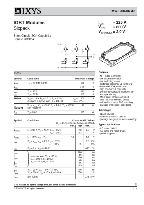
48IXYS reserves the right to change limits, test conditions and dimensions.Features•NPT IGBT technology •low saturation voltage •low switching losses•switching frequency up to 30 kHz •square RBSOA, no latch up •high short circuit capability•positive temperature coefficient for easy parallelling•MOS input, voltage controlled •ultra fast free wheeling diodes •solderable pins for PCB mounting •package with copper base plate Advantages•space savings•reduced protection circuits•package designed for wave soldering Typical Applications •AC motor control•AC servo and robot drives •power suppliesSymbol Conditions Maximum RatingsV CES T VJ = 25°C to 150°C600V V GES ± 20V I C25T C = 25°C 225A I C80T C = 80°C155A RBSOA V GE = ±15 V; R G = 1.5 Ω; T VJ = 125°C I CM = 400A Clamped inductive load; L = 100 µH V CEK ≤ V CESt SCV CE = V CES ; V GE = ±15 V; R G = 1.5 Ω; T VJ = 125°C 10µs (SCSOA)non-repetitive P totT C = 25°C675WSymbol ConditionsCharacteristic Values(T= 25°C, unless otherwise specified)I C25= 225 AV CES= 600 V V CE(sat) typ.= 2.0 VIGBT Modules SixpackShort Circuit SOA CapabilitySquare RBSOA17191548Symbol Conditions Maximum Ratings T VJ operating-40...+125°C T JM +150°C T stg -40...+125°C V ISOL I ISOL ≤ 1 mA; 50/60 Hz 2500V~M dMounting torque (M5) 3 - 6NmSymbol ConditionsCharacteristic Values min.typ.max.R pin-chip 1.8m Ωd S Creepage distance on surface 10mmd A Strike distance in air 10mmR thCH with heatsink compound0.01K/W Weight300gSymbol Conditions Maximum RatingsI F25T C = 25°C 260A I F80T C = 80°C165ASymbol ConditionsCharacteristic ValuesEquivalent Circuits for SimulationConductionIGBT (typ. at V GE = 15 V; T J = 125°C)V 0 = 1.1 V; R 0 = 6 m ΩFree wheeling Diode (typ. at T J = 125°C)V 0 = 1.1 V; R 0 = 2 m ΩThermal ResponseIGBT (typ.)C th1 = 0.397 J/K; R th1 = 0.131 K/W C th2 = 2.243 J/K; R th2 = 0.049 K/W Free wheeling Diode (typ.)C th1 = 0.281 J/K; R th1 = 0.236 K/W C th2 = 1.945 J/K; R th2 = 0.064 K/W48012340123450100150200250300V CEV V CEA V Q G-di/dt67891011120100200300400V V GEA I C0120100200300400500600VV FI F A Fig. 1Typ. output characteristics Fig. 2Typ. output characteristicsFig. 3Typ. transfer characteristics Fig. 4Typ. forward characteristics of free wheeling diodeFig. 5Typ. turn on gate charge Fig. 6Typ. turn off characteristics offree wheeling diode448Fig. 11Reverse biased safe operating area RBSOA Fig. 12Typ. transient thermal impedanceFig. 8Typ. turn off energyversus collector currentFig.10Typ. turn off energyversus gate resistor01002003004004812160.00010.0010.010.11100.0010.010.110481216202468100200300400500600700I CA R GΩV CEts mJ VmJ。
LM2940中文资料
LM2940-5.0低压差三端稳压芯片(国产)型号:LM2940-5.0P+封装:TO-220输出电压固定的低压差三端稳压器;输出电压5V;输出电流1A;输出电流1A时,最小输入输出电压差小于0.8V;最大输入电压26V;工作温度-40~+125℃;内含静态电流降低电路、电流限制、过热保护、电池反接和反插入保护电路。
LM2940引脚图LM2940-5.0的参数介绍:首先是基本介绍也就是general description,从这可以了解到2940最大输出电流有1A,典型的输入输出电压压降为0.5V,还有就是过流保护,过压保护这样一般电源芯片都有的东西LM2940典型应用由图可见,2940的电路接发极其简单。
接着比较重要的参数就是dropout voltage,也就是输入输出压降由表可知,LM2940-5.0在输出电流为1A时dropout voltage典型值为0.5V,即输入电压要>输出电压+0.5V=5.5V;同样输出电流为100mA时dropout voltage典型值为110mV,输入电压大于5.1V即可接下去的就是比较重要的一些图,依次介绍下这个图表示2940的输入电压瞬间改变时输出电压的变化情况,由图可知输出电压在10uS 内即可恢复正常上图为输入电压低于正常值时,输入电压与输出电压间的关系(输出电流均保持在1A时)上图为输入电压大于限定值时输出电压的情况,由图可得,输入电压大于30V时芯片启动了过压保护功能,输出电压在此刻变为0VLM2940和7805的区别:LM2940比7805的转换效率高。
7805直接输入不接输出的情况下,其内部还会有3mA的电流消耗(静态电流)。
而LDO元件的静态电流就比它远远小得多了。
具体请看LDO的解释。
LM2940就是一个LDO。
LM2940中文资料
LM2940中文资料LM2940-5.0低压差三端压压芯片;压,国型,号LM2940-5.0P+封,装TO-220压出压压固定的低压差三端压压器~压出压压5V~压出压流1A~压出压流1A 压~最小压入压出压压差小于0.8V~最大压入压压26V~工作度温-40,+125?~含压压流降低压路、压流限制、压压保压、压池反内静接和反入保压压路。
插LM2940引脚压LM2940-5.0的介压,参数首先是基本介压也就是general description~压可以了解到从2940最大压出压流有1A~典型的压入压出压压压降压0.5V~压有就是压流保压~压压保压压压一般压源芯片都有的压西接着就是典型压路压~一般接压直接按照典型压路压接就来 OK 了~同压上压LM2940典型压用由压可压~2940的压路接压其压压。
极接着比压重要的就是参数dropout voltage~也就是压入压出压降由表可知~LM2940-5.0在压出压流压1A压dropout voltage典型压压0.5V~压入压压要即>压出压压+0.5V=5.5V~同压压出压流压100mA压dropout voltage 典型压压110mV~压入压压大于5.1V可即接下去的就是比压重要的一些压~依次介压下压压表示个2940的压入压压瞬压改压压压出压压的压化情~由压可知压出压压在况10uS可恢压正常内即上压压压入压压低于正常压压~压入压压压出压压压的压系;压出压流均保持在与1A压,上压压压入压压大于限定压压压出压压的情~由压可得~压入压压大于况30V 压芯片压了压压保压功能~压出压启压在此刻压压0VLM2940和7805的压,区LM2940比7805的压压效率高。
7805直接压入不接压出的情下~其部压有况内会3mA的压流消耗;压压流,。
而静LDO元件的压压流就比压压小得多了。
具压看静它体LDO的解压。
LM2940就是一个LDO。
中文版-ISO-178-2010

中文版-ISO-178-2010ISO 178-2010塑料——弯曲性能的测定1.范围1.1本国际标准规定了在特定条件下测定硬质(见3.12)和半硬质塑料弯曲性能的方法。
规定了标准试样尺寸,同时对适合使用的替代试样也提供了尺寸参数。
规定了试验速度范围。
1.2本标准用于在规定条件下研究试样弯曲特性,测定弯曲强度、弯曲模量和其他弯曲应力/应变关系。
本标准适用于两端自由支撑、中央加荷的试验(三点加载测试)。
1.3本标准适用于下列材料:——热塑性模塑、挤出铸造材料,包括填充和增强复合物;硬质热塑性板材;——热固性模塑材料,包括填充和增强复合物;热固性板材。
与ISO 10350-1[5]和ISO 10350-2[6]一致,本国际标准适用于测试以长度≤7.5 mm纤维增强的复合物。
对于纤维长度>7.5 mm的长纤维增强材料(层压材料)的测试,见ISO 14125[7]。
本标准通常不适用于硬质多孔材料和含有多孔材料的夹层结构材料。
对这些材料的测试,可1.4弯曲测试更合适于测试具有较小断裂挠度的坚硬材料和脆性材料。
1.5与本国际标准的之前版本相反,本版本包含了方法A和方法B两个方法。
方法A与本国际标准的之前版本中的方法一致,即在试验中使用1%/min的变形速度。
方法B使用两个不同的变形速度:弯曲模量测试中选用1%/min 的速度,测量弯曲应力-应变曲线的剩余部分依材料延展性的不同而选用5%/min或50%/min的形变速度。
2.规范性引用文件本文件中引用了以下的文件。
对于标示日期的引用文件,只有引用的版本有效。
对于未标示日期的文献,其最新版(包括任何修正)适用于本标准。
ISO 291,塑料——状态调节与测试标准环境ISO 293,塑料——热塑性材料的压塑试样ISO 294-1:1996,塑料——热塑性材料注塑试样——第1部分:一般原理及多用途和长条试样的模塑成型。
ISO 295,塑料——热固性材料的压塑试样ISO 2602,测试结果的统计处理和解释——均值估计——置信区间ISO 2818,塑料——机械加工制备试样ISO 7500-1,金属材料——静态单轴测试仪器验证——第1部分:张力/压缩测试机器——力测量系统的验证和校准ISO 9513,金属材料——单轴测试伸长计校正ISO 10724-1,塑料——热固性粉末模塑复合物试样的注射模塑成型——第1部分:一般原则和多用途试样的模塑成型ISO 16012,塑料——试样线性尺寸的测定ISO 20753,塑料——试样ISO 23529,橡胶——物理实验方法试样的准备和状态调节的通用步骤2术语和定义下列术语和定义适用于本标准。
- 1、下载文档前请自行甄别文档内容的完整性,平台不提供额外的编辑、内容补充、找答案等附加服务。
- 2、"仅部分预览"的文档,不可在线预览部分如存在完整性等问题,可反馈申请退款(可完整预览的文档不适用该条件!)。
- 3、如文档侵犯您的权益,请联系客服反馈,我们会尽快为您处理(人工客服工作时间:9:00-18:30)。
Vsat H + VsatL Total Saturation Voltage Ileakage K VDIAG IDIAG Vpin 8 Vpin 10 VSENS Output Leakage Current On Time Limiter Constant (°) Diagnostic Output Voltage (pin 5) Diagnostic Leakage Current (pin 5) OP AMP and OTA CD Voltage Gain (°°) Sensing Voltage (pin 10) (°°°)
3/8
元器件交易网
L294
CIRCUIT OPERATION The L294 work as a trasconductance amplifier: it can supply an output current directly proportional to an input voltage level (Vi). Fyrthermore, it allows complete switching control of the output current waveform (see fig. 1). The following explanation refers to the Block Diagram, to fig. 1 and to the typical application circuit of fig. 2. The ton time is fixed by the width of the Enable input signal (TTL compatible): it is active low and enables the output stages "source" and "sink". At the end of ton, the load current Iload recirculates through D1 and D2, allowing fast current turn-off. The rise time tr, depends on the load characteristics, on Vi and on the supply voltage value (Vs, pin 1). During the ton time, Iload is converter into a voltage signal by means of the external sensing resistance Rs connected to pin 10. This signal, amplified by the op amp and converted by the transconductance amplifier OTA, charges the external RC network at pin 8 (R1, C1). The voltage at this pin is sensed by the inverting input of a comparator. The voltage on the non-inverting input of this one is fixed by the external voltage Vi (pin 7). After tr, the comparator switches and the output stage "source" is switched off. The comaprator output is confirmed by the voltage on the non-inverting input, which decreases of a costant fraction of Vi (1/10), allowing hysteresis operation. The current in the load now flow through D1. Two Cases are possible: the time constant of the recirculation phase is higher than R1.C1; the time constant is lower than R1.C1. In the first case, the voltage sensed in the non-inverting input of the comparator is just the value proportional to Iload. In the second case, when the current decreases too quickly, the comparator senses the voltage signal stored in the R1 C1 network. In the first case t1 depends on the load characteristics, while in the second case it depends only on the value of R1. C1. In the other words, R1. C1 fixes the minimum value of t1 )t1 ≥ 1/10 R1.C1. Note that C1 should be chosen in the range 2.7 to 10 nF for stability reasons of the OTA). After t1, the comparator switches again: the output is confirmed by the voltage on the non-inverting input, which reaches Vi again (hysteresis). Now the cycle starts again: t2, t4 and t6 have the same characteristics as tr, while t3 and t5 are similar to t1. The peak current Ip depends on Vi as shown in the typical transfer function of fig.3. It can be seen that for Vi lower than 450 mV the device is not operating. For Vi greater than 600 mV, the L294 has a transconductance of 1A/V with Rs = 0.2Ω. For Vi included between 450 and 600 mV, the operation is not guaranteed. The order parts of the device have protection and diagnostic functions. At pin 3 is connected an external capacitor C2, charged at costant current when the Enable is low. After a time interval equal to K C2 (K is defined in the table of Electrical Characteristics and has the dimensions of ohms) the output stages are switched off independently by the Input signal. This avoids the load being driven in conduction for an excessive period of time (overdriving protection). The action of this protection is shown in fig. 1b. Note that the voltage ramp at pin 3 starts whenever the Enable signal becomes active (low state), regardless of the Input signal. To reset pin 3 and to restore the normal conditions, pin 9 must return high. This protection can be disabled by grounding pin 3. The thermal protection included in the L294 has a hysteresis. It switches off the output stages whenever the junction temperature increases too much. After a fall of about 20°C, the circuit starts again. Finally, the device is protected against any type of short circuit at the outputs: to ground, to supply and across the load. When the source stage current is higher than 5A and/or when the pin 10 voltage is higher then 1V (i.e. for a sink current greater than 1V/Rs) the output stages are switched off and the device is inhibited. This condition is indicated at the open-collector output DIAG (pin 5); the internal flip-flop F/F changes and forces the output transistor into saturation. The F/F must be supplied independently through Vss (pin 4). The DIAG signal is reset and the output stages are still operative by switching the device on again. After that, two cases are possible: the reason for the "bad operation" is still present and the protection acts again; the reason has been removed and the device starts to work properly.