5082-H153-KN000中文资料
5082-7403-FFZ00资料

7.6 mm (0.3 inch) Micro Bright Seven Segment Displays Technical DataFeatures• Available with Colon for Clock Display • Compact Package 0.300 x 0.500 inchesLeads on 2.54 mm (0.1 inch)Centers• Choice of Colors AlGaAs Red, HighEfficiency Red, Yellow, Green,Orange• Excellent Appearance Evenly Lighted Segments Mitered Corners on Segments Surface Color Gives Optimum Contrast±50° Viewing Angle • Design FlexibilityCommon Anode or Common CathodeRight Hand Decimal Point ±1. Overflow Character • Categorized for Luminous IntensityYellow and Green Categorized for ColorUse of Like Categories Yields a Uniform Display • High Light Output • High Peak Current• Excellent for Long Digit String Multiplexing • Intensity and Color Selection Available See Intensity and ColorSelected Displays Data Sheet • Sunlight Viewable AlGaAsDescriptionThe 7.6 mm (0.3 inch) LED seven segment displays are designed for viewing distances up to 3 metres (10 feet). These devices use an industry standard size package and pinout. Both the numeric andDevicesOrange AlGaAs [1]HER [1]Yellow [1]Green [1]Package HDSP-HDSP-HDSP-HDSP-HDSP- DescriptionDrawingA401A151750174017801Common Anode Right A Hand Decimal750274027802Common Anode Right Hand B Decimal, Colon A403A153750374037803Common Cathode Right C Hand Decimal750474047804Common Cathode Right Hand D Decimal, ColonA157750774077807Common Anode ±1. Overflow E A158750874087808Common Cathode ±1. OverflowFNote:1. These displays are recommended for high ambient light operation. Please refer to the HDSP-A10X AlGaAs, HDSP-335X HER, HDSP-A80X Yellow, and HDSP-A90X Green data sheet for low current operation.HDSP-740x Series HDSP-750x Series HDSP-780x Series HDSP-A15x Series HDSP-A40x Series±1. overflow devices feature a right hand decimal point. All devices are available as either common anode or common cathode.These displays are ideal for most applications. Pin for pin equiv-alent displays are also available in a low current design. The low current displays are ideal forportable applications. For additional information see the Low Current Seven Segment Displays.Part Numbering SystemNotes:1. For codes not listed in the figure above, please refer to the respective datasheet or contact your nearest Agilent representative for details.2. Bin options refer to shippable bins for a part number. Color and Intensity Bins are typically restricted to 1bin per tube (exceptions may apply). Please refer to respective datasheet for specific bin limit information.5082 -X X X X-X X X X X HDSP-X X X X-X X X X XMechanical Options [1]00: No Mechanical OptionColor Bin Options [1,2]0: No Color Bin Limitation3: Color Bins 3- and 3+ only (applicable for Yellow devices only)Z: Color Bins 2- and 3+ only (applicable for Yellow devices only)Maximum Intensity Bin [1,2]0: No Maximum Intensity Bin Limitation Minimum Intensity Bin [1,2]0: No Minimum Intensity Bin Limitation Device Configuration/Color [1]1: Common Anode 2: Common Anode 3: Common Cathode 4: Common CathodeDevice Specific Configuration [1]Refer to Respective DatasheetPackage [1]A: 7.6 mm (0.3 inch) Single Digit Seven Segment DisplayPackage Dimensions NOTES:1. ALL DIMENSIONS IN MILLIMETRES (INCHES).2. MAXIMUM.3. ALL UNTOLERANCED DIMENSIONS AREFOR REFERENCE ONLY.4. REDUNDANT ANODES.5. REDUNDANT CATHODES.6. FOR HDSP-7400/-7800 SERIES PRODUCT ONLY.Device Series HDSP-ParameterSymbol Min.Typ.Max.Units Test Conditions Luminous Intensity/Segment [1,2,5]I V6.914.0mcd I F = 20 mA (Digit Average)1.8VI F = 20 mAForward Voltage/Segment or DPV F2.03.0V I F = 100 mAA15xPeak Wavelength λPEAK 645nm Dominant Wavelength [3]λd 637nm Reverse Voltage/Segment or DP [4]V R 3.015.0V I R = 100 µA Temperature Coefficient of ∆V F /°C -2mV/°C V F /Segment or DPThermal Resistance LED Junction-R θJ-PIN255°C/W/Segto-PinAlGaAs RedElectrical/Optical Characteristics at T A = 25°C Absolute Maximum RatingsAlGaAs Red HER/Orange Yellow GreenHDSP-A150HDSP-7500/-A40X HDSP-7400HDSP-7800DescriptionSeriesSeries SeriesSeriesUnits Average Power per Segment or DP 9610580105mW Peak Forward Current per 160[1]90[3]60[5]90[7]mA Segment or DPDC Forward Current per 40[2]30[4]20[6]30[8]mASegment or DPOperating Temperature Range –20 to +100[9]–40 to +100°CStorage Temperature Range –55 to +100°C Reverse Voltage per Segment or DP 3.0V Lead Solder Temperature for 3Seconds (1.59 mm [0.063 in.] 260°Cbelow seating plane)Notes:1. See Figure 1 to establish pulsed conditions.2. Derate above 46°C at 0.54 mA/°C.3. See Figure 6 to establish pulsed conditions.4. Derate above 53°C at 0.45 mA/°C.5. See Figure 7 to establish pulsed conditions.6. Derate above 81°C at 0.52 mA/°C.7. See Figure 8 to establish pulsed conditions.8. Derate above 39°C at 0.37 mA/°C.9. For operation below –20°C, contact your local Agilent components sales office or an authorized distributor.High Efficiency RedDeviceSeriesHDSP-Parameter Symbol Min.Typ.Max.Units Test Conditions Luminous Intensity/Segment[1,2,6]360980I F = 5 mA(Digit Average)I Vµcd5390I F = 20 mA Forward Voltage/Segment or DP V F 2.0 2.5V I F = 20 mA 750x Peak WavelengthλPEAK635nmDominant Wavelength[3]λd626nmReverse Voltage/Segment or DP[4]V R 3.030V I R = 100 µATemperature Coefficient of∆V F/°C-2mV/°CV F/Segment or DPThermal Resistance LED Junction-RθJ-PIN200°C/W/Segto-PinOrangeDeviceSeriesHDSP-Parameter Symbol Min.Typ.Max.Units Test Conditions Luminous Intensity/Segment[1,2,6]I V0.70mcd I F = 5 mA(Digit Average)Forward Voltage/Segment or DP V F 2.0 2.5V I F = 20 mA A40x Peak WavelengthλPEAK600nmDominant Wavelength[3]λd603nmReverse Voltage/Segment or DP[4]V R 3.030V I R = 100 µATemperature Coefficient of∆V F/°C-2mV/°CV F/Segment or DPThermal Resistance LED Junction-RθJ-PIN200°C/W/Segto-PinYellowDeviceSeriesHDSP-Parameter Symbol Min.Typ.Max.Units Test Conditions Luminous Intensity/Segment[1,2,7]225480I F = 5 mA(Digit Average)I Vµcd2740I F = 20 mA Forward Voltage/Segment or DP V F 2.2 2.5V I F = 20 mA 740x Peak WavelengthλPEAK583nmDominant Wavelength[3,9]λd581.5586592.5nmReverse Voltage/Segment or DP[4]V R 3.050.0V I R = 100 µATemperature Coefficient of∆V F/°C-2mV/°CV F/Segment or DPThermal Resistance LED Junction-RθJ-PIN200°C/W/Segto-PinHigh Performance GreenDeviceSeriesHDSP-Parameter Symbol Min.Typ.Max.Units Test Conditions Luminous Intensity/Segment[1,2,8]8603000I F = 10 mA(Digit Average)I Vµcd6800I F = 20 mA Forward Voltage/Segment or DP V F 2.1 2.5V I F = 10 mA 780x Peak WavelengthλPEAK566nmDominant Wavelength[3,9]λd571577nmReverse Voltage/Segment or DP[4]V R 3.050.0V I R = 100 µATemperature Coefficient of∆V F/°C-2mV/°CV F/Segment or DPThermal Resistance LED Junction-RθJ-PIN200°C/W/Segto-PinNotes:1. Case temperature of device immediately prior to the intensity measurement is 25°C.2. The digits are categorized for luminous intensity. The intensity category is designated by a letter on the side of the package.3. The dominant wavelength, λd, is derived from the CIE chromaticity diagram and is that single wavelength which defines the color ofthe device.4. Typical specification for reference only. Do not exceed absolute maximum ratings.5. For low current operation the AlGaAs HDSP-A101 series displays are recommended.6. For low current operation the HER HDSP-7511 series displays are recommended.7. For low current operation the Yellow HDSP-A801 series displays are recommended.8. For low current operation the Green HDSP-A901 series displays are recommended.9. The yellow (HDSP-7400) and Green (HDSP-7800) displays are categorized for dominant wavelength. The category is designated by anumber adjacent to the luminous intensity category letter.AlGaAs Redt – PULSE DURATION – µs P101100R A T I O O F M A X I M U M O P E R A T I N G P E A K C U R R E N T T O T E M P E R A T U R E D E R A T E D M A X I M U M D C C U R R E N TI P E A K F I M A X DC Figure 4. Relative Luminous Intensity vs. DC Forward Current.Figure 2. Maximum Allowable DC Current per Segment as a Function of Ambient Temperature.Figure 1. Maximum Allowed Peak Current vs.Pulse Duration – AlGaAs Red.Figure 5. Relative Efficiency (LuminousIntensity per Unit Current) vs. Peak Current.Figure 3. Forward Current vs.Forward Voltage.T A – AMBIENT TEMPERATURE – °C I D C M A X . – M A X I M U M D C C U R R E N T P E R S E G M E N T– m AV F – FORWARD CURRENT – VI F – F O R W A R D C U R R E N T P E R S E G M E N T – m AI PEAK – PEAK FORWARD CURRENT PER SEGMENT – mAηP E A K – N O R M A L I Z E D R E L A T I V E E F F I C I E N C YI F – FORWARD CURRENT PER SEGMENT – mA R E L A T I V E L U M I N O U S I N T E N S I T Y (N O R M A L I Z E D T O 1 A T 20 m A )Figure 12. Relative Efficiency (Luminous Intensity per Unit Current) vs. Peak Current.ηP E A K – R E L A T I V E E F F I C I E N C Y (N O R M A L I Z E D T O 1 A T 5 m A F O R H E R ,O R A N G E A N D Y E L L O W , A N D 10 m A F O R G R E E N )I PEAK – PEAK FORWARD CURRENTPER SEGMENT – mAHER, Yellow, Green, OrangeFigure 6. Maximum Tolerable Peak Current vs.Pulse Duration – HER, Orange.Figure 7. Maximum Tolerable Peak Current vs. Pulse Duration – Yellow.Figure 10. Forward Current vs.Forward Voltage Characteristics.Figure 11. Relative LuminousIntensity vs. DC Forward Current.Figure 8. Allowable Peak Current vs.Pulse Duration – Green.Figure 9. Maximum Allowable DC Current per Segment as a Function of Ambient Temperature.R A T I O O F M A X I M U M O P E R A T I N G P E A K C U R R E N T T O T E M P E R A T U R E D E R A T E D D C C U R R E N TI P E A K F I M A X D C t – PULSE DURATION – µs P 101100DCR A T I O O F M A X I M U M O P E R A T I N G P E A K C U R R E N T T O T E M P E R A T U R E D E R A T E D D C C U R R E N TI P E A K FI M A X D C t – PULSE DURATION – µs P101100R A T I O O F M A X I M U M O P E R A T I N G P E A K C U R R E N T T O T E M P E R A T U R E D E R A T E D D C C U R R E N TI P E A K FI M A X D C t – PULSE DURATION – µs P10110040051015202530352010090807060504030T – AMBIENT TEMPERATURE – °C AI M A X –M A X I M U M D C C U R R E N T P E R S E G M E N T – m AD C120110504510080604020I – F O R W A R D C U R R E N T P E R S E G M E N T – m A FV – FORWARD VOLTAGE – V F R E L A T I V E L U M I N O U S I N T E N S I T Y (N O R M A L I Z E D T O 1 A T 5 m A F O R H E R A N D )t (Y E L L O W A N D T O1 A T 10 m A F O R G R E E N )1510205301025I – FORWARD CURRENT PER SEGMENT – mA FHDSP-A15x IV Bin Category Min.Max.M 7.0713.00N 10.6019.40O 15.9029.20P 23.9043.80Q 35.8065.60Intensity Bin Limits (mcd)AlGaAs RedHDSP-750x IV Bin Category Min.Max.B 0.3420.630C 0.5160.946D 0.774 1.418E 1.160 2.127F 1.740 3.190G 2.610 4.785H 3.9157.177HERHDSP-740x IV Bin Category Min.Max.B 0.2290.387C 0.3170.582D 0.4760.872E 0.714 1.311F 1.073 1.967G 1.609 2.950H 2.4134.425YellowHDSP-780x IV Bin Category Min.Max.H 0.86 1.58I 1.29 2.37J 1.94 3.55K 2.90 5.33L 4.378.01GreenOrangeHDSP-A40XIV Bin Category Min.Max.A 0.2840.433B 0.3540.541C 0.4430.677D 0.5540.846E 0.692 1.057F 0.856 1.322G 1.082 1.652H 1.352 2.066I 1.692 2.581J 2.114 3.227K 2.641 4.034L 3.300 5.042M 4.127 6.303N 5.1577.878Color CategoriesNote:All categories are established for classification of products. Products may not be available in all categories. Please contact your Agilent representatives for further clarification/information.Contrast EnhancementFor information on contrastenhancement, please seeApplication Note 1015.Soldering/CleaningCleaning agents from the ketonefamily (acetone, methyl ethylketone, etc.) and from thechlorinated hydrocarbon family(methylene chloride, trichloro-ethylene, carbon tetrachloride,etc.) are not recommended forcleaning LED parts. All of thesevarious solvents attack or dissolvethe encapsulating epoxies used toform the package of plastic LEDparts.For further information onsoldering LEDs, please refer toApplication Note 1027.元器件交易网/semiconductorsFor product information and a complete list ofdistributors, please go to our web site.For technical assistance call:Americas/Canada: +1 (800) 235-0312 or(408) 654-8675Europe: +49 (0) 6441 92460China: 10800 650 0017Hong Kong: (+65) 271 2451India, Australia, New Zealand: (+65) 271 2394Japan: (+81 3) 3335-8152(Domestic/Interna-tional), or 0120-61-1280(Domestic Only)Korea: (+65) 271 2194Malaysia, Singapore: (+65) 271 2054Taiwan: (+65) 271 2654Data subject to change.Copyright © 2002 Agilent Technologies, Inc.Obsoletes 5988-0382ENFebruary 11, 20025988-4434EN。
5082-2800中文资料

Schottky Barrier Diodes for General Purpose ApplicationsTechnical DataFeatures• Low Turn-On VoltageAs Low as 0.34 V at 1 mA• Pico Second Switching Speed • High Breakdown VoltageUp to 70 V• Matched Characteristics AvailableDescription/Applications The 1N5711, 1N5712, 5082-2800/ 10/11 are passivated Schottky barrier diodes which use a patented “guard ring” design to achieve a high breakdown voltage. Packaged in a low cost glass package, they are well suited for high level detecting, mixing, switching, gating, log or A-D converting, video detecting, frequency discriminating, sampling, and wave shaping.The 5082-2835 is a passivatedSchottky diode in a low cost glasspackage. It is optimized for lowturn-on voltage. The 5082-2835 isparticularly well suited for theUHF mixing needs of the CATVmarketplace.The 5082-2300 Series and5082-2900 devices are unpas-sivated Schottky diodes in a glasspackage. These diodes haveextremely low 1/f noise and areideal for low noise mixing, andhigh sensitivity detecting. Theyare particularly well suited for usein Doppler or narrow band videoreceivers.1N57111N57125082-2300 Series5082-2800 Series5082-2900DIMENSIONS IN MILLIMETERS AND (INCHES).Outline 15Maximum RatingsJunction Operating and Storage Temperature Range5082-2303, -2900.................................................................-60°C to +100°C 1N5711, 1N5712, 5082-2800/10/11....................................-65°C to +200°C 5082-2835............................................................................-60°C to +150°C DC Power Dissipation(Measured in an infinite heat sink at T CASE = 25°C)Derate linearly to zero at maximum rated temperature5082-2303, -2900..............................................................................100 mW 1N5711, 1N5712, 5082-2800/10/11.................................................250 mW 5082-2835.........................................................................................150 mW Peak Inverse Voltage.................................................................................V BRPackage CharacteristicsOutline 15Lead Material........................................................................................DumetLead Finish..............................................................................95-5% Tin-LeadMax. Soldering Temperature................................................260°C for 5 secMin. Lead Strength....................................................................4 pounds pullTypical Package Inductance1N5711, 1N5712:................................................................................2.0 nH2800 Series:........................................................................................2.0 nH2300 Series, 2900:..............................................................................3.0 nHTypical Package Capacitance1N5711, 1N5712:................................................................................0.2 pF2800 Series:........................................................................................0.2 pF2300 Series, 2900:............................................................................0.07 pFThe leads on the Outline 15 package should be restricted so that thebend starts at least 1/16 inch from the glass body.Outline 15 diodes are available on tape and reel. The tape and reelspecification is patterned after RS-296-D.Electrical Specifications at T= 25°CAGeneral Purpose DiodesMin.Max.V F = 1 V Max.Max.Max.Breakdown Forward at Forward Reverse Leakage Capaci-Part Package Voltage Voltage Current Current tance Number Outline V BR (V)V F (mV)I F (mA)I R (nA) at V R (V)C T (pF) 5082-280015704101520050 2.0 1N571115704101520050 2.0 5082-281015204103510015 1.2 1N571215205503515016 1.2 5082-28111515410201008 1.2 5082-2835158*34010*1001 1.0 Test I R = 10 µA I F = 1 mA*V F = 0.45 V V R = 0 V Conditions*I R = 100 µA f =1.0 MHz Note: Effective Carrier Lifetime (τ) for all these diodes is 100 ps maximum measured with Krakauer method at 5 mA except for 5082-2835 which is measured at 20 mA.Low 1/f (Flicker) Noise DiodesMin.Max.V F = 1 V Max.Max.Max.Part Breakdown Forward at Forward Reverse Leakage Capaci-Number Package Voltage Voltage Current Current tance 5082-Outline V BR (V)V F (mV)I F (mA)I R (nA) at V R (V)C T (pF) 230315204003550015 1.0 29001510400201005 1.2 Test I R = 10 µA I F = 1 mA V R = 0 V Conditions f =1.0 MHzNote: Effective Carrier Lifetime (τ) for all these diodes is 100 ps maximum measured with Krakauer method at 20 mA.Matched Pairs and QuadsBasic Matched MatchedPart Number Pair Quad Batch5082-Unconnected Unconnected Matched[1]Test Conditions2900∆VF at IF= 1.0, 10 mA28005082-28045082-2805∆V F at I F = 0.5, 5 mA ∆V F = 20 mV∆V F = 20 mV*I F = 10 mA∆C O at f = 1.0 MHz28115082-2826∆VF at IF= 10 mA∆V F = 10 mV∆C O at f = 1.0 MHz ∆C O = 0.1 pF28355082-2080∆VF at IF=10 mA∆V F = 10 mV∆C O at f = 1.0 MHz∆C O = 0.1 pFNote:1. Batch matched devices have a minimum batch size of 50 devices.SPICE ParametersParameter Units5082-28005082-28105082-28115082-28355082-23035082-2900B V V75251892510C J0pF 1.60.8 1.00.70.7 1.1E G eV0.690.690.690.690.690.69I BV A10E-510E-510E-510E-510E-510E-5I S A 2.2 x 10E-9 1.1 x 10E-90.3 x 10E-8 2.2 x 10E-87 x 1.0E-910E-8N 1.08 1.08 1.08 1.08 1.08 1.08 R SΩ25101051015 P B V0.60.60.60.560.640.64 PT222222 M0.50.50.50.50.50.5Typical ParametersV F – FORWARD VOLTAGE (V)Figure 1. I-V Curve Showing Typical Temperature Variation for 5082-2300 Series and 5082-2900 Schottky Diodes.1001010.10.01I F - F O R W A R D C U R R E N T (m A )V BR (V)Figure 2. 5082-2300 Series Typical Reverse Current vs. Reverse Voltage at Various Temperatures.10.0001,000100101I R (n A )051015100755025T A = 25°CI F - FORWARD CURRENT (mA)Figure 3. 5082-2300 Series and 5082-2900 Typical Dynamic Resistance (R D ) vs. Forward Current (I F ).100010010R D - D Y N A M I C R E S I S T AN C E (Ω)0.01010100V R - REVERSE VOLTAGE (V)Figure 4. 5082-2300 and 5082-2900 Typical Capacitance vs. Reverse Voltage.1.21.00.80.60.40.20C T - C A P A C I T A N C E (p F )048121620V F - FORWARD VOLTAGE (V)Figure 5. I-V Curve Showing Typical Temperature Variation for 5082-2800 or 1N5711 Schottky Diodes.5010510.50.10.050.01I F - F O R W A R D C U R R E N T (m A )00.20.40.60.8 1.0 1.2V R - REVERSE VOLTAGE (V)Figure 6. (5082-2800 OR 1N5711) Typical Variation of Reverse Current (I R ) vs. Reverse Voltage (V R ) at Various Temperatures.100,00010,0001000100101I R - R E V E R S E C U R R E N T (n A )0.20.40.60.81.01.2V R - REVERSE VOLTAGE (V)Figure 7. (5082-2800 or 1N5711)Typical Capacitance (C T ) vs. Reverse Voltage (V R ).12.01.51.00.50C T - C A P A C I T A N C E (p F )010********V F - FORWARD VOLTAGE (V)Figure 8. I-V Curve Showing Typical Temperature Variation for the 5082-2810 or 1N5712 Schottky Diode.100101.00.10.01I F - F O R W A R D C U R R E N T (m A )V R - REVERSE VOLTAGE (V)Figure 9. (5082-2810 or IN5712)Typical Variation of Reverse Current (I R ) vs. Reverse Voltage (V R ) at Various Temperatures.10,0001000100101.0I R - R E V E R S E C U R R E N T (n A )Typical Parameters, continuedV F - FORWARD VOLTAGE (V)Figure 10. I-V Curve Showing Typical Temperature Variation for the 5082-2811 Schottky Diode.100101.00.10.01I F - F O R W A R D C U R R E N T (m A )0.40.20.60.81.01.2V R - REVERSE VOLTAGE (V)Figure 11. (5082-2811) Typical Variation of Reverse Current (I R ) vs. Reverse Voltage (V R ) at Various Temperatures.100,00010,0001000100101I R - R E V E R S E C U R R E N T (n A )0510********V F - FORWARD VOLTAGE (V)Figure 12. I-V Curve Showing Typical Temperature Variations for 5082-2835 Schottky Diode.100101.00.10.01I F - F O R W A R D C U R R E N T (m A )00.20.40.60.8 1.0 1.2V R - REVERSE VOLTAGE (V)Figure 13. (5082-2835) Typical Variation of Reverse Current (I R ) vs. Reverse Voltage (V R ) at Various Temperatures.100,00010,0001000100101I R - R E V E R S E C U R R E N T (n A )0123456V R - REVERSE VOLTAGE (V)Figure 14. Typical Capacitance (C T ) vs. Reverse Voltage (V R ).C T - C A P A C I T A N C E (p F )0246810I F - FORWARD CURRENT (mA)Figure 15. Typical Dynamic Resistance (R D ) vs. Forward Current (I F ).1000100101R D - D Y N A M I C R E S I S T A N C E (Ω)Diode Package Marking1N5xxx5082-xxxxwould be marked:1Nx xxxxx xxYWW YWWwhere xxxx are the last four digits of the 1Nxxxx or the 5082-xxxx partnumber. Y is the last digit of the calendar year. WW is the work week ofmanufacture.Examples of diodes manufactured during workweek45 of 1999:1N57125082-3080would be marked:1N53071280945945Data subject to change.Copyright © 1999 Agilent TechnologiesObsoletes 5968-4304E5968-7181E (11/99)。
5082-B09G-LL300中文资料
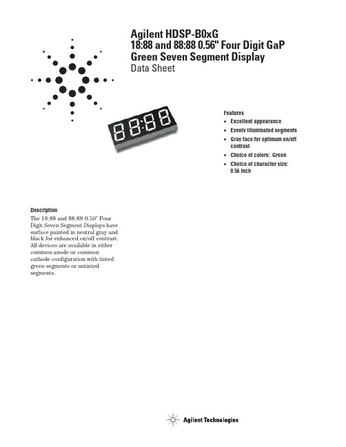
DescriptionThe 18:88 and 88:88 0.56" Four Digit Seven Segment Displays have surface painted in neutral gray and black for enhanced on/off contrast. All devices are available in either common anode or common cathode configuration with tinted green segments or untinted segments.Agilent HDSP-B0xG18:88 and 88:88 0.56" Four Digit GaP Green Seven Segment DisplayData SheetFeatures•Excellent appearance•Evenly illuminated segments•Gray face for optimum on/offcontrast•Choice of colors: Green•Choice of character size:0.56 inchFRONT SIDE2 – ∅1.70RIGHT SIDEA A A DDD C F EF E F EB CB C B C GGGDP3DP2DIGIT 2DIGIT 3DIGIT 4DIGIT 1AF EB G D NOTE:ALL DIMENSIONS ARE IN MILLIMETERS (INCHES).UNLESS OTHERWISE STATED, TOLERANCES ARE ± 0.25 mm.Pin Configuration Function Pin HDSP-B01G/B03G/B05G/B07G/B09G HDSP-B02G/B04G/B06G/B08G/B10G 1Anode E Cathode E 2Anode D Cathode D 3Anode DP Cathode DP 4Anode C Cathode C 5Anode GCathode G6Digit 4 Common Cathode Digit 4 Common Anode 7Anode BCathode B8Digit 3 Common Cathode Digit 3 Common Anode 9Digit 2 Common Cathode Digit 2 Common Anode 10Anode F Cathode F 11Anode ACathode A12Digit 1 Common CathodeDigit 1 Common AnodeFRONT SIDE2 – ∅1.70RIGHT SIDEAA A DDD B CF EF E F EB CB C B C GGGDP3DP2DIGIT 2DIGIT 3DIGIT 4DIGIT 1NOTE:ALL DIMENSIONS ARE IN MILLIMETERS (INCHES).UNLESS OTHERWISE STATED, TOLERANCES ARE ± 0.25 mm.HDSP-B01G and HDSP-B05G (Common Cathode)HDSP-B02G and HDSP-B06G (Common Anode)DIGIT 1DIGIT 2DIGIT 3DIGIT 4A 11B 7C 4D 2E 1F 10G 5DP 3DIGIT 1DIGIT 2DIGIT 3DIGIT 4A 11B 7C 4D 2E 1F 10G 5DP 3HDSP-B03G, HDSP-B07G, and HDSP-B09G (Common Cathode)HDSP-B04G, HDSP-B08G, and HDSP-B10G (Common Anode)DIGIT 1DIGIT 2DIGIT 3DIGIT 4A 11B 7C 4D 2E 1F 10G 5DP3DIGIT 1DIGIT 2DIGIT 3DIGIT 4A 11B 7C 4D 2E 1F 10G 5DP 3DevicesHDSP-DescriptionB01G88:88 0.56" Green 4 Digit, Tinted Green, Common Cathode, Display 18:88, Gray Color Surface B02G88:88 0.56" Green 4 Digit, Tinted Green, Common Anode, Display 18:88, Gray Color Surface B03G88:88 0.56" Green 4 Digit, Tinted Green, Common Cathode, Display 88:88, Gray Color Surface B04G88:88 0.56" Green 4 Digit, Tinted Green, Common Anode, Display 88:88, Gray Color Surface B05G88:88 0.56" Green 4 Digit, Untinted, Common Cathode, Display 18:88, Gray Color SurfaceB06G88:88 0.56" Green 4 Digit, Untinted, Common Anode, Display 18:88, Gray Color SurfaceB07G88:88 0.56" Green 4 Digit, Untinted, Common Cathode, Display 88:88, Gray Color SurfaceB08G88:88 0.56" Green 4 Digit, Untinted, Common Anode, Display 88:88, Gray Color SurfaceB09G88:88 0.56" Green 4 Digit, Untinted, Common Cathode, Display 88:88, Black Color SurfaceB10G88:88 0.56" Green 4 Digit, Untinted, Common Anode, Display 88:88, Black Color SurfacePart Numbering System5082 -X X X X-X X X X XHDSP-X X X X-X X X X XMechanical Options[1]00: No Mechanical OptionColor Bin Options[1,2]0: No Color Bin LimitationMaximum Intensity Bin[1,2]0: No Maximum Intensity Bin LimitationMinimum Intensity Bin[1,2]0: No Minimum Intensity Bin LimitationDevice Configuration/Color[1]G: GreenDevice Specific Configuration[1]Refer to Respective DatasheetPackage[1]Refer to Respective DatasheetNotes:1. For codes not listed in the figure above, please refer to the respective datasheet or contactyour nearest Agilent representative for details.2. Bin options refer to shippable bins for a part number. Color and Intensity Bins are typicallyrestricted to 1 bin per tube (exceptions may apply). Please refer to respective datasheet forspecific bin limit information.Electrical/Optical Characteristics at T A = 25˚C Device Series HDSP-ParameterSymbol Min.Typ.Max.Units Test Conditions Luminous Intensity/SegmentI V20003200µcd I F = 10 mA(Digit Average)32004500All DevicesForward Voltage/Segment or DP V F 1.802.20 2.60V I F = 20 mA Peak Wavelength λPEAK 568nm I F = 20 mA Dominant Wavelength λd 573nmI F = 20 mA Luminous Intensity I V-M 2:1I F = 10 mA Matching Ratio Reverse CurrentI R100µAV R = 5 VNotes:1.Typical specification for reference only. Do not exceed absolute maximum ratings.2.The dominant wavelength, λd , is derived from the CIE chromaticity diagram and is that single wavelength which defines the color of the device.Absolute Maximum RatingsDescriptionGreen Units Average Power per Segment or DP65mW Peak Forward Current per Segment or DP 100mA DC Forward Current per Segment or DP 25mA Operating Temperature Range–40 to +105˚C Storage Temperature Range–40 to +105˚C Reverse Voltage per Segment or DP5V Wavesoldering Temperature for 3 seconds 2 mm below body250˚CNote:1.Derate above 40˚C at 0.33 mA/˚C for green.B01G, B02G, B03G, B04G B05G, B06G, B07G, B08G,B09G, B10G Intensity Bin Limits (µcd at 10 mA)Device Series HDSP-B01G, B02G, B03G, B04G B05G, B06G, B07G, B08G, B09G, B10GBin Name Min.[1]Max.[1]Min.[1]Max.[1]K 20003200NA NA L 3200505032005050MNA NA50508000Note:1.Tolerance for each bin limit is ±10%.Color Categories (Tolerance ± 1 nm)Rank Symbol Hue Range Unit 22573.5–576.5nm 33570.5–573.5nmContrast EnhancementFor information on contrast enhancement, please see Application Note 1015.Soldering/CleaningCleaning agents from the ketone family (acetone, methyl ethyl ketone, etc.) and from thechlorinated hydrocarbon family (methylene chloride,trichloroethylene, carbon tetrachloride, etc.) are notrecommended for cleaning LED parts. All these various solvents attack or dissolve theencapsulating epoxies used to form the package of plastic LED parts.Figure 1. Maximum allowable DC current vs.ambient temperature.Figure 2. Forward current vs. forward voltage.Figure 3. Relative luminous intensity vs. DC forward current.Figure 4. Relative efficiency (luminous intensity per unit current) vs. peak current.I D C – M A X I M U M D C C U R R E N T P E R S E G M E N T – m AT A – AMBIENT TEMPERATURE – °CI F – F O R W A R D C U R R E N T P E R S E G M E NT – m AV F – FORWARD VOLTAGE – VR E L A T I V E L U M I N O U S I N T E N S I T Y (N O R M A L I Z E D T O 1 A T 10 mA F O R G R E E N )I F – DC FORWARD CURRENT – mA8642R E L A T I V E E F F I C I E N C Y (N O R M A L I Z E D T O 1 A T 10 m A )1.4005101520253035404550PEAK FORWARD CURRENTPER SEGMENT – mA/semiconductorsFor product information and a complete list of distributors, please go to our web site.For technical assistance call:Americas/Canada: +1 (800) 235-0312 or (916) 788-6763Europe: +49 (0) 6441 92460China: 10800 650 0017Hong Kong: (+65) 6756 2394India, Australia, New Zealand: (+65) 6755 1939Japan: (+81 3) 3335-8152(Domestic/Interna-tional), or 0120-61-1280(Domestic Only)Korea: (+65) 6755 1989Singapore, Malaysia, Vietnam, Thailand,Philippines, Indonesia: (+65) 6755 2044Taiwan: (+65) 6755 1843Data subject to change.Copyright © 2004 Agilent Technologies, Inc.Obsoletes 5988-5381EN June 30, 20045988-7859EN。
热电偶热电阻保护套管选用材质参考表
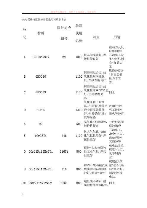
热电偶热电阻保护套管选用材质参考表标记材质国外对应钢号最高使用温度特点用途A1Cr18Ni9Ti321800抗晶间腐蚀好,焊接性能良好核动力及反应堆构件\石油化工设备\造纸\制皂\食品加工B GH30301100镍基高温合金.抗氧化性耐腐蚀优良,焊接性能良好.燃烧炉设备\在高温低压力下工作.C GH30391150镍基高温合金.抗氧化性比GH3030更好,使用温度更高 .同上D PtRH61300氧化条件下耐高温,在卤素\酸等溶液中耐腐蚀性能好,但易受碳\硅\硫等污染玻璃行业\代工熔炉\退火等炉窑E20500易氧化\不耐腐蚀,但价格便宜一般低温无腐蚀场合F1Cr25Ti4461100抗大气氧化,抗硫化气氛性能好,焊接性能好石油化工,冶金\电力\热处理炉\焚烧炉等G0Cr18Ni12Mo2Ti316Ti800耐酸\盐水核腐蚀性工业气氛,焊接性能好核电站及反应堆\化工\化学制药业.H0Cr17Ni12Mo2Ti316800耐酒石酸\磷酸\硫酸腐蚀\抗晶间腐蚀好,焊接性能好硫酸盐\纸浆\纺织\染料\制皂业\制药业\核电站.HL00Cr17Ni12Mo2316L800超低碳不锈钢,耐腐蚀性能比316好,同上焊接性能好.I H62200强度较好,导热性好,易于焊接低温无腐蚀场合J0Cr18Ni9304400低碳不锈钢,耐晶间腐蚀性能和焊接性能良好化工\纺织\造纸\制皂业\食品加工\硝酸工业\核电站JL00Cr18Ni10304L400低碳不锈钢,耐腐蚀性能比304好,焊接性能良好同上K0Cr21Ni32TiAl Incocloy8001100若热稳定性好,氧化皮不易脱落,抗渗碳核渗氮电站\炉窑\原油和石油化工N1Cr15Ni75Fe Incone16001100镍铬铁合金,耐腐蚀性能好,高温抗氧化,焊接性能好.核电站\锅炉\炉窑\热处理\造纸业\食品加工O00Cr15Ni60Mo16W哈氏C-276700耐点蚀,抗晶间腐蚀,高温力学性能良好精细化工\石油化工P1Cr25Ni20310S1200抗腐蚀性能好,耐氯蚀同温抗氧化锅炉\ 鼓风炉\水泥炉窑\原油和石油化工\高温硫化床\电站T CYT1011200精型高温合金,具有较高的强度和耐磨性能.具有很好的抗硫化能力,抗氧化能力优异,是何在高温腐蚀性气氛中使用,焊接性能\加工性能好燃烧炉\热交换器\锅炉\炉窑\造纸业\高温流化床\电站R CB1钢玉质1600陶瓷保护管.耐高温\耐酸碱,能在腐蚀性介质中使用,但不能承受碰撞,易脆断高温加热炉等场合Q CB2高铝质1300陶瓷保护管,性能与刚玉管相同,但同上使用温度较低M MoSi2二硅化相1600金属陶瓷保护管.耐高温\抗腐蚀\气密性好\.耐热冲击\抗冲刷\但脆性大石油化工\天然气\水泥\冶金\机械行业等高温腐蚀场合S SiC再结晶碳化硅1600非金属陶瓷保护管,高温抗氧化\耐腐蚀\抗热冲击\抗冲刷\但脆性大冶金\玻璃\水泥等工业炉窑SS SiC-Si新型碳化硅1400非金属陶瓷保护管.强度大\耐腐蚀\抗氧化\耐磨损\热导率高能承受急剧的温度变化冶金\玻璃\水泥等工业炉窑以及要求耐磨的场合。
5082-B03G-0L000中文资料

DescriptionThe 18:88 and 88:88 0.56" Four Digit Seven Segment Displays have surface painted in neutral gray and black for enhanced on/off contrast. All devices are available in either common anode or common cathode configuration with tinted green segments or untinted segments.Agilent HDSP-B0xG18:88 and 88:88 0.56" Four Digit GaP Green Seven Segment DisplayData SheetFeatures•Excellent appearance•Evenly illuminated segments•Gray face for optimum on/offcontrast•Choice of colors: Green•Choice of character size:0.56 inchFRONT SIDE2 – ∅1.70RIGHT SIDEA A A DDD C F EF E F EB CB C B C GGGDP3DP2DIGIT 2DIGIT 3DIGIT 4DIGIT 1AF EB G D NOTE:ALL DIMENSIONS ARE IN MILLIMETERS (INCHES).UNLESS OTHERWISE STATED, TOLERANCES ARE ± 0.25 mm.Pin Configuration Function Pin HDSP-B01G/B03G/B05G/B07G/B09G HDSP-B02G/B04G/B06G/B08G/B10G 1Anode E Cathode E 2Anode D Cathode D 3Anode DP Cathode DP 4Anode C Cathode C 5Anode GCathode G6Digit 4 Common Cathode Digit 4 Common Anode 7Anode BCathode B8Digit 3 Common Cathode Digit 3 Common Anode 9Digit 2 Common Cathode Digit 2 Common Anode 10Anode F Cathode F 11Anode ACathode A12Digit 1 Common CathodeDigit 1 Common AnodeFRONT SIDE2 – ∅1.70RIGHT SIDEAA A DDD B CF EF E F EB CB C B C GGGDP3DP2DIGIT 2DIGIT 3DIGIT 4DIGIT 1NOTE:ALL DIMENSIONS ARE IN MILLIMETERS (INCHES).UNLESS OTHERWISE STATED, TOLERANCES ARE ± 0.25 mm.HDSP-B01G and HDSP-B05G (Common Cathode)HDSP-B02G and HDSP-B06G (Common Anode)DIGIT 1DIGIT 2DIGIT 3DIGIT 4A 11B 7C 4D 2E 1F 10G 5DP 3DIGIT 1DIGIT 2DIGIT 3DIGIT 4A 11B 7C 4D 2E 1F 10G 5DP 3HDSP-B03G, HDSP-B07G, and HDSP-B09G (Common Cathode)HDSP-B04G, HDSP-B08G, and HDSP-B10G (Common Anode)DIGIT 1DIGIT 2DIGIT 3DIGIT 4A 11B 7C 4D 2E 1F 10G 5DP3DIGIT 1DIGIT 2DIGIT 3DIGIT 4A 11B 7C 4D 2E 1F 10G 5DP 3DevicesHDSP-DescriptionB01G88:88 0.56" Green 4 Digit, Tinted Green, Common Cathode, Display 18:88, Gray Color Surface B02G88:88 0.56" Green 4 Digit, Tinted Green, Common Anode, Display 18:88, Gray Color Surface B03G88:88 0.56" Green 4 Digit, Tinted Green, Common Cathode, Display 88:88, Gray Color Surface B04G88:88 0.56" Green 4 Digit, Tinted Green, Common Anode, Display 88:88, Gray Color Surface B05G88:88 0.56" Green 4 Digit, Untinted, Common Cathode, Display 18:88, Gray Color SurfaceB06G88:88 0.56" Green 4 Digit, Untinted, Common Anode, Display 18:88, Gray Color SurfaceB07G88:88 0.56" Green 4 Digit, Untinted, Common Cathode, Display 88:88, Gray Color SurfaceB08G88:88 0.56" Green 4 Digit, Untinted, Common Anode, Display 88:88, Gray Color SurfaceB09G88:88 0.56" Green 4 Digit, Untinted, Common Cathode, Display 88:88, Black Color SurfaceB10G88:88 0.56" Green 4 Digit, Untinted, Common Anode, Display 88:88, Black Color SurfacePart Numbering System5082 -X X X X-X X X X XHDSP-X X X X-X X X X XMechanical Options[1]00: No Mechanical OptionColor Bin Options[1,2]0: No Color Bin LimitationMaximum Intensity Bin[1,2]0: No Maximum Intensity Bin LimitationMinimum Intensity Bin[1,2]0: No Minimum Intensity Bin LimitationDevice Configuration/Color[1]G: GreenDevice Specific Configuration[1]Refer to Respective DatasheetPackage[1]Refer to Respective DatasheetNotes:1. For codes not listed in the figure above, please refer to the respective datasheet or contactyour nearest Agilent representative for details.2. Bin options refer to shippable bins for a part number. Color and Intensity Bins are typicallyrestricted to 1 bin per tube (exceptions may apply). Please refer to respective datasheet forspecific bin limit information.Electrical/Optical Characteristics at T A = 25˚C Device Series HDSP-ParameterSymbol Min.Typ.Max.Units Test Conditions Luminous Intensity/SegmentI V20003200µcd I F = 10 mA(Digit Average)32004500All DevicesForward Voltage/Segment or DP V F 1.802.20 2.60V I F = 20 mA Peak Wavelength λPEAK 568nm I F = 20 mA Dominant Wavelength λd 573nmI F = 20 mA Luminous Intensity I V-M 2:1I F = 10 mA Matching Ratio Reverse CurrentI R100µAV R = 5 VNotes:1.Typical specification for reference only. Do not exceed absolute maximum ratings.2.The dominant wavelength, λd , is derived from the CIE chromaticity diagram and is that single wavelength which defines the color of the device.Absolute Maximum RatingsDescriptionGreen Units Average Power per Segment or DP65mW Peak Forward Current per Segment or DP 100mA DC Forward Current per Segment or DP 25mA Operating Temperature Range–40 to +105˚C Storage Temperature Range–40 to +105˚C Reverse Voltage per Segment or DP5V Wavesoldering Temperature for 3 seconds 2 mm below body250˚CNote:1.Derate above 40˚C at 0.33 mA/˚C for green.B01G, B02G, B03G, B04G B05G, B06G, B07G, B08G,B09G, B10G Intensity Bin Limits (µcd at 10 mA)Device Series HDSP-B01G, B02G, B03G, B04G B05G, B06G, B07G, B08G, B09G, B10GBin Name Min.[1]Max.[1]Min.[1]Max.[1]K 20003200NA NA L 3200505032005050MNA NA50508000Note:1.Tolerance for each bin limit is ±10%.Color Categories (Tolerance ± 1 nm)Rank Symbol Hue Range Unit 22573.5–576.5nm 33570.5–573.5nmContrast EnhancementFor information on contrast enhancement, please see Application Note 1015.Soldering/CleaningCleaning agents from the ketone family (acetone, methyl ethyl ketone, etc.) and from thechlorinated hydrocarbon family (methylene chloride,trichloroethylene, carbon tetrachloride, etc.) are notrecommended for cleaning LED parts. All these various solvents attack or dissolve theencapsulating epoxies used to form the package of plastic LED parts.Figure 1. Maximum allowable DC current vs.ambient temperature.Figure 2. Forward current vs. forward voltage.Figure 3. Relative luminous intensity vs. DC forward current.Figure 4. Relative efficiency (luminous intensity per unit current) vs. peak current.I D C – M A X I M U M D C C U R R E N T P E R S E G M E N T – m AT A – AMBIENT TEMPERATURE – °CI F – F O R W A R D C U R R E N T P E R S E G M E NT – m AV F – FORWARD VOLTAGE – VR E L A T I V E L U M I N O U S I N T E N S I T Y (N O R M A L I Z E D T O 1 A T 10 mA F O R G R E E N )I F – DC FORWARD CURRENT – mA8642R E L A T I V E E F F I C I E N C Y (N O R M A L I Z E D T O 1 A T 10 m A )1.4005101520253035404550PEAK FORWARD CURRENTPER SEGMENT – mA/semiconductorsFor product information and a complete list of distributors, please go to our web site.For technical assistance call:Americas/Canada: +1 (800) 235-0312 or (916) 788-6763Europe: +49 (0) 6441 92460China: 10800 650 0017Hong Kong: (+65) 6756 2394India, Australia, New Zealand: (+65) 6755 1939Japan: (+81 3) 3335-8152(Domestic/Interna-tional), or 0120-61-1280(Domestic Only)Korea: (+65) 6755 1989Singapore, Malaysia, Vietnam, Thailand,Philippines, Indonesia: (+65) 6755 2044Taiwan: (+65) 6755 1843Data subject to change.Copyright © 2004 Agilent Technologies, Inc.Obsoletes 5988-5381EN June 30, 20045988-7859EN。
5082-5523-FK000中文资料
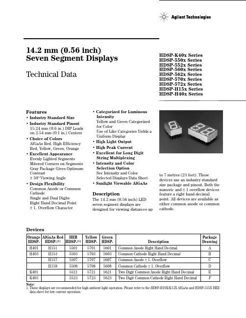
14.2 mm (0.56 inch)Seven Segment Displays Technical DataFeatures• Industry Standard Size • Industry Standard Pinout 15.24 mm (0.6 in.) DIP Leads on 2.54 mm (0.1 in.) Centers • Choice of ColorsAlGaAs Red, High Efficiency Red, Yellow, Green, Orange • Excellent Appearance Evenly Lighted Segments Mitered Corners on Segments Gray Package Gives Optimum Contrast±50° Viewing Angle • Design FlexibilityCommon Anode or Common CathodeSingle and Dual Digits Right Hand Decimal Point ±1. Overflow Character• Categorized for Luminous IntensityYellow and Green Categorized for ColorUse of Like Categories Yields a Uniform Display • High Light Output • High Peak Current• Excellent for Long Digit String Multiplexing • Intensity and Color Selection OptionSee Intensity and ColorSelected Displays Data Sheet • Sunlight Viewable AlGaAsDescriptionThe 14.2 mm (0.56 inch) LED seven segment displays aredesigned for viewing distances upto 7 metres (23 feet). Thesedevices use an industry standard size package and pinout. Both the numeric and ±1 overflow devices feature a right hand decimalpoint. All devices are available as either common anode or common cathode.Orange AlGaAs Red HERYellowGreen Package HDSP-HDSP-[1]HDSP-[1]HDSP-HDSP- DescriptionDrawingH401H151550157015601Common Anode Right Hand Decimal A H403H153550357035603Common Cathode Right Hand Decimal B H157550757075607Common Anode ±1. Overflow C H158550857085608Common Cathode ±1. OverflowD K401552157215621Two Digit Common Anode Right Hand DecimalE K403552357235623Two Digit Common Cathode Right Hand DecimalFDevicesNote:1. These displays are recommended for high ambient light operation. Please refer to the HDSP-H10X/K12X AlGaAs and HDSP-555X HER data sheet for low current operation.HDSP-K40x Series HDSP-550x Series HDSP-552x Series HDSP-560x Series HDSP-562x Series HDSP-570x Series HDSP-572x Series HDSP-H15x Series HDSP-H40x SeriesThese displays are ideal for most applications. Pin for pin equivalent displays are alsoavailable in a low current design.The low current displays are idealfor portable applications. For additional information see the Low Current Seven Segment Displays data sheet.Part Numbering SystemNotes:1. For codes not listed in the figure above, please refer to the respective datasheet or contact your nearest Agilent representative for details.2. Bin options refer to shippable bins for a part number. Color and Intensity Bins are typically restricted to 1bin per tube (exceptions may apply). Please refer to respective datasheet for specific bin limit information.5082 -X X X X-X X X X X HDSP-X X X X-X X X X XMechanical Options [1]00: No Mechanical Option Color Bin Options [1,2]0: No Color Bin LimitationMaximum Intensity Bin [1,2]0: No Maximum Intensity Bin Limitation Minimum Intensity Bin [1,2]0: No Minimum Intensity Bin Limitation Device Configuration/Color [1]1: Common Anode 3: Common CathodeDevice Specific Configuration [1]Refer to Respective DatasheetPackage [1]H: 14.2 mm (0.56 inch) Single Digit Seven Segment DisplayFUNCTIONPIN AB CDEF1CATHODE e ANODE e CATHODE c ANODE cE CATHODE NO. 1 E ANODE NO. 12CATHODE d ANODE d ANODE c, d CATHODE c, d D CATHODE NO. 1 D ANODE NO. 13ANODE [3]CATHODE [4]CATHODE b ANODE bC CATHODE NO. 1 C ANODE NO. 14CATHODE c ANODE c ANODE a, b, DP CATHODE a, b, DP DP CATHODE NO. 1DP ANODE NO. 15CATHODE DP ANODE DP CATHOPDE DP ANODE DE E CATHODE NO. 1 E ANODE NO. 26CATHODE b ANODE b CATHODE a ANODE aD CATHODE NO. 2 D ANODE NO. 27CATHODE a ANODE a ANODE a, b, DP CATHODE a, b, DP G CATHODE NO. 2G ANODE NO. 28ANODE [3]CATHODE [4]ANODE c, d CATHODE c, d C CATHODE NO. 2 C ANODE NO. 29CATHODE f ANODE f CATHODE d ANODE d DP CATHODE NO. 2DP ANODE NO. 210CATHODE g ANODE g NO PINNO PINB CATHODE NO. 2 B ANODE NO. 211 A CATHODE NO. 2 A ANODE NO. 212 F CATHODE NO. 2 F ANODE NO. 213DIGIT NO. 2 ANODE DIGIT NO. 2 CATHODE 14DIGIT NO. 1 ANODE DIGIT NO. 1 CATHODE 15 B CATHODE NO. 1 B ANODE NO. 116 A CATHODE NO. 1 A ANODE NO. 117G CATHODE NO. 1G ANODE NO. 118F CATHODE NO. 1 F ANODE NO. 1NOTES:1. ALL DIMENSIONS IN MILLIMETRES (INCHES).2. ALL UNTOLERANCED DIMENSIONS ARE FOR REFERENCE ONLY.3. REDUNDANT ANODES.4. REDUNDANT CATHODES.5. FOR HDSP-5600/-5700 SERIES PRODUCT ONLY.Package DimensionsInternal Circuit DiagramNotes:1. See Figure 2 to establish pulsed conditions.2. Derate above 46°C at 0.54 mA/°C.3. See Figure 7 to establish pulsed conditions.4. Derate above 53°C at 0.45 mA/°C.5. See Figure 8 to establish pulsed conditions.HER/Orange HDSP-5500AlGaAs Red HDSP-H40x Yellow Green HDSP-H150HDSP-K40x HDSP-5700HDSP-5600 Description SeriesSeriesSeriesSeriesUnits Average Power per Segment or DP 9610580105mW Peak Forward Current per 160[1]90[3]60[5]90[7]mA Segment or DPDC Forward Current per Segment or DP 40[2]30[4]20[6]3018]mA Operating Temperature Range -20 to +100[9]-40 to +100°C Storage Temperature Range -55 to +100°C Reverse Voltage per Segment or DP 3.0V Lead Solder Temperature for 3 Seconds 260°C(1.60 mm [0.063 in.] below seating plane)Absolute Maximum Ratings6. Derate above 81°C at 0.52 mA/°C.7. See Figure 9 to establish pulsed conditions.8. Derate above 39°C at 0.37 mA/°C.9. For operation below -20°C, contact your local Agilent components sales office or an authorized distributor.Electrical/Optical Characteristics at T A = 25°CAlGaAs RedDeviceSeriesHDSP- Parameter Symbol Min.Typ.Max.Units Test Conditions Luminous Intensity/Segment[1,2,5]I V9.116.0mcd I F = 20 mA(Digit Average)1.8I F = 20 mAForward Voltage/Segment or DP V F V2.03.0I F = 100 mAH15XPeak WavelengthλPEAK645nmDominant Wavelength[3]λd637nmReverse Voltage/Segment or DP[4]V R 3.015V I R = 100 µATemperature Coefficient of∆V F/°C-2mV/°CV F/Segment or DPThermal Resistance LED Junction-RθJ-Pin400°C/W/to-Pin SegHigh Efficiency RedDeviceSeriesHDSP- Parameter Symbol Min.Typ.Max.Units Test Conditions9002800I F = 10 mA Luminous Intensity/Segment[1,2,6]I Vµcd(Digit Average)3700I F = 60 mA Peak:1 of 6 dfForward Voltage/Segment or DP V F 2.1 2.5V I F = 20 mA 55XXPeak WavelengthλPEAK635nmDominant Wavelength[3]λd626nmReverse Voltage/Segment or DP[4]V R 3.030V I R = 100 µATemperature Coefficient of∆V F/°C-2mV/°CV F/Segment or DPThermal Resistance LED Junction-RθJ-Pin345°C/W/to-Pin SegYellowDeviceSeriesHDSP- Parameter Symbol Min.Typ.Max.Units Test Conditions6001800I F = 10 mA Luminous Intensity/Segment[1,2]I Vµcd(Digit Average)2750I F = 60 mA Peak:1 of 6 dfForward Voltage/Segment or DP V F 2.1 2.5V I F = 20 mA 57XXPeak WavelengthλPEAK583nmDominant Wavelength[3,7]λd581.5586592.5nmReverse Voltage/Segment or DP[4]V R 3.040V I R = 100 µATemperature Coefficient of∆V F/°C-2mV/°CV F/Segment or DPThermal Resistance LED Junction-RθJ-Pin345°C/W/to-Pin SegOrangeDeviceSeriesHDSP- Parameter Symbol Min.Typ.Max.Units Test Conditions Luminous Intensity/Segment I V 2.37mcd I F = 10 mA(Segment Average)[1,2]Forward Voltage/Segment or DP V F 2.1 2.5V I F = 20 mAPeak WavelengthλPEAK600nm H40x Dominant Wavelength[3]λd603nm I F = 10 mA K40x Reverse Voltage/Segment or DP[4]V R 3.030V I R = 100 µA Temperature Coefficient of∆V F/°C-2mV/°CV F/Segment or DPThermal Resistance LED Junction-RθJ-Pin345°C/W/to-Pin SegDeviceSeries HDSP-ParameterSymbol Min.Typ.Max.UnitsTest Conditions 9002500I F = 10 mALuminous Intensity/Segment [1,2]I Vµcd(Digit Average)`3100I F = 60 mA Peak:1 of 6 df Forward Voltage/Segment or DPV F 2.1 2.5V I F = 10 mA56XXPeak Wavelength λPEAK 566nm Dominant Wavelength [3,7]λd 571577nm Reverse Voltage/Segment or DP [4]V R 3.050V I R = 100 µATemperature Coefficient of ∆V F /°C -2mV/°C V F /Segment or DPThermal Resistance LED Junction-R θJ-Pin345°C/W/to-PinSegHigh Performance GreenNotes:1. Device case temperature is 25°C prior to the intensity measurement.2. The digits are categorized for luminous intensity. The intensity category is designated by a letter on the side of the package.3. The dominant wavelength, λd , is derived from the CIE chromaticity diagram and is that single wavelength which defines the color of the device.4. Typical specification for reference only. Do not exceed absolute maximum ratings.5. For low current operation, the AlGaAs HDSP-H10X series displays are recommended. They are tested at 1 mA dc/segment and are pin for pin compatible with the HDSP-H15X series.6. For low current operation, the HER HDSP-555X series displays are recommended. They are tested at 2 mA dc/segment and are pin for pin compatible with the HDSP-550X series.7. The Yellow (HDSP-5700) and Green (HDSP-5600) displays are categorized for dominant wavelength. The category is designated by a number adjacent to the luminous intensity category letter.AlGaAs RedFigure 2. Maximum Tolerable Peak Current vs. Pulse Duration – AlGaAs Red.Figure 1. Maximum Tolerable Peak Current vs.Pulse Duration – Red.Figure 3. Maximum Allowable DC Current vs.Ambient Temperature.Figure 4. Forward Current vs.Forward Voltage.HER, Yellow, Green, OrangeFigure 7. Maximum Tolerable Peak Currentvs. Pulse Duration – HER, Orange.Figure 8. Maximum Tolerable Peak Current vs. Pulse Duration – Yellow.Figure 5. Relative Luminous Intensity vs. DC Forward Current.Figure 6. Relative Efficiency (Luminous Intensity per Unit Current) vs. Peak Current.I D C M A X . – M A X I M U M D C C U R R E N T P E R S E G M E N T – m AT A – AMBIENT TEMPERATURE – °C 5030102051525354045I F – F O R W A R D C U R R E N T P E R S E G M E N T – m AV F – FORWARD VOLTAGE – VR E L A T I V E L U M I N O U S I N T E N S I T Y (N O R M A L I Z E D T O 1 A T 20 m A )I F – FORWARD CURRENT PER SEGMENT – mA204010305152535ηP E A K – N O R M A L IZ E D R E L A T I V E E F F I C I E N C YI PEAK – PEAK FORWARD CURRENTPER SEGMENT – mA40051015202530352010090807060504030T – AMBIENT TEMPERATURE – °C AI M A X – M A X I M U M D C C U R R E N T P E R S E G M E N T – m AD C 4550110120Figure 11. Forward Current vs.Forward Voltage.Figure 9. Maximum Tolerable PeakCurrent vs. Pulse Duration – Green.Figure 10. Maximum Allowable DC Current vs.Ambient Temperature.Figure 12. Relative LuminousIntensity vs. DC Forward Current.Figure 13. Relative Efficiency (Luminous Intensity per Unit Current) vs. Peak Current.Electrical/OpticalFor more information onelectrical/optical characteristics,please see Application Note 1005.Contrast EnhancementFor information on contrastenhancement please see Application Note 1015.Soldering/CleaningCleaning agents from the ketone family (acetone, methyl ethyl ketone, etc.) and from thechlorinated hydrocarbon family(methylene chloride, trichloro–ethylene, carbon tetrachloride,etc.) are not recommended for cleaning LED parts. All of these various solvents attack or dissolve the encapsulating epoxies used to form the package of plastic LED parts.For information on soldering LEDs please refer to Application Note 1027.I F – F O R W A R D C U R R E N T P E R S E G M E N T – m AV F – FORWARD VOLTAGE – VR E L A T I V E L U M I N O U S I N T E N S I T Y (N O R M A L I Z E D A T 10 m A )I F – DC FORWARD CURRENT – mAηV – R E L A T I V E E F F I C I E N C Y (N O R M A L I Z E D T O 1 A T 10 m A P E R S E G M EN T )0.6I PEAK – PEAK FORWARD CURRENTPER SEGMENT – mA902070801001.61.41.31.10.90.860504030100.71.01.21.5HDSP-H15x IV Bin Category Min.Max.K 9.2016.90L 13.8025.30M 20.7038.00N 31.1056.90O 46.6085.40Intensity Bin Limits (mcd)AlGaAs RedHDSP-550x/552x IV Bin Category Min.Max.E 0.91 1.67F 1.37 2.51G 2.05 3.76H 3.08 5.64I 4.628.64J 6.9312.70K 10.3919.04HERHDSP-570x/572xIV Bin Category Min.Max.D 0.61 1.11E 0.91 1.67F 1.37 2.51G 2.05 3.76H 3.08 5.64I 4.628.64J 6.9312.70K 10.3919.04YellowHDSP-560x/562x IV Bin Category Min.Max.E 0.91 1.67F 1.37 2.51G 2.05 3.76H 3.08 5.64I 4.618.46GreenColor CategoriesNote:All categories are established for classification of products. Products may not be available in all categories. Please contact your Agilent representatives for further clarification/information.10HDSP-H40x/K40x IV Bin Category Min.Max.B 0.77 1.17C 0.95 1.45D 1.19 1.82E 1.49 2.27F 1.85 2.89G 2.32 3.54H 2.904.43Orange元器件交易网元器件交易网/semiconductorsFor product information and a complete list ofdistributors, please go to our web site.For technical assistance call:Americas/Canada: +1 (800) 235-0312 or(408) 654-8675Europe: +49 (0) 6441 92460China: 10800 650 0017Hong Kong: (+65) 271 2451India, Australia, New Zealand: (+65) 271 2394Japan: (+81 3) 3335-8152(Domestic/Interna-tional), or 0120-61-1280(Domestic Only)Korea: (+65) 271 2194Malaysia, Singapore: (+65) 271 2054Taiwan: (+65) 271 2654Data subject to change.Copyright © 2002 Agilent Technologies, Inc.Obsoletes 5988-0383ENJanuary 17, 20025988-4273EN。
5082-A411-HM000资料

DevicesAlGaAs Orange Red HER Green Package HDSP-HDSP-HDSP-HDSP- DescriptionDrawingA411A111A211A5117.6 mm Common Anode Right Hand Decimal A A413A113A213A5137.6 mm Common Cathode Right Hand Decimal B F411F111F211F51110 mm Common Anode Right Hand Decimal C F413F113F213F51310 mm Common Cathode Right Hand Decimal D G411G111G211G51110 mm Two Digit Common Anode Right Hand Decimal E G413G113G213G51310 mm Two Digit Common Cathode Right Hand Decimal F H411H111H211H51114.2 mm Common Anode Right Hand Decimal G H413H113H213H51314.2 mm Common Cathode Right Hand Decimal H K411K111K211K51114.2 mm Two Digit Common Anode Right Hand Decimal I K413K113K213K51314.2 mm Two Digit Common Cathode Right Hand DecimalJBlack Surface Seven Segment Displays Technical DataFeatures• Black Surface and Color Tinted Epoxy• Industry Standard Size • Industry Standard Pinout • Choice of Character Size 7.6 mm (0.30 in.), 10 mm (0.40in.), 14.2 mm (0.56 in.)• Choice of ColorsAlGaAs Red, High Efficiency Red (HER), Green, Orange • Excellent Appearance Evenly Lighted Segments ±50° Viewing Angle• Design FlexibilityCommon Anode or Common CathodeSingle and Two Digit• Categorized for Luminous IntensityCategorized for Color: Green Use of Like Categories Yields a Uniform Display• Excellent for Long Digit String MultiplexingDescriptionThese devices use industrystandard size package and pinout.Available with black surfaceHDSP-AX11/-AX13 Series HDSP-FX11/-FX13 Series HDSP-GX11/-GX13 Series HDSP-HX11/-HX13 Series HDSP-KX11/-KX13 Seriesfinish. All devices are available as either common anode or common cathode.Typical applications includeappliances, channel indicators of TV, CATV converters, game machines, and point of sale terminals.Part Numbering System5082 -X X X X-X X X X XHDSP-X X X X-X X X X XMechanical Options[1]00: No Mechanical OptionColor Bin Options[1,2]0: No Color Bin LimitationMaximum Intensity Bin[1,2]0: No Maximum Intensity Bin LimitationMinimum Intensity Bin[1,2]0: No Minimum Intensity Bin LimitationDevice Configuration/Color[1]1: Common Anode3: Common CathodeDevice Specific Configuration[1]Refer to Respective DatasheetPackage[1]A: 7.6 mm (0.3 inch) Single Digit Seven Segment DisplayF: 10 mm (0.4 inch) Single Digit Seven Segment DisplayG: 10 mm (0.4 inch) Dual Digit Seven Segment DisplayH: 14.2 mm (0.56 inch) Single Digit Seven Segment DisplayK: 14.2 mm (0.56 inch) Dual Digit Seven Segment Display Notes:1. For codes not listed in the figure above, please refer to the respective datasheet or contact your nearestAgilent representative for details.2. Bin options refer to shippable bins for a part number. Color and Intensity Bins are typically restricted to 1bin per tube (exceptions may apply). Please refer to respective datasheet for specific bin limit information.Package Dimensions (7.6 mm Series)Internal Circuit DiagramPackage Dimensions (10 mm Series: Single)Internal Circuit DiagramPackage Dimensions (10 mm Series: Two Digit)Internal Circuit DiagramPackage Dimensions (14.2 mm Series: Single)Internal Circuit DiagramPackage Dimensions (14.2 mm Series: Two Digit)Internal Circuit Diagram2DIGIT NO. 1 CATHODE1Absolute Maximum RatingsAlGaAs Red HER/Orange GreenHDSP-X11X HDSP-X21X/X41X HDSP-X51X Description Series Series Series Units Average Power per Segment37105105mW or DPPeak Forward Current per4590[1]90[3]mA Segment or DPDC Forward Current per15[5]30[2]30[4]mA Segment or DPOperating Temperature Range–20 to +100 –40 to +100°C Storage Temperature Range–55 to +100°C Reverse Voltage per 3.0V Segment or DPWave Soldering Temperature for250°C 3 Seconds (1.60 mm [0.063 in.]below Body)Notes:1. See Figure 5 to establish pulsed conditions.2. Derate above 53°C at 0.45 mA/°C (see Figure 7).3. See Figure 6 to establish pulsed conditions.4. Derate above 39°C at 0.37 mA/°C (see Figure 7).5. Derate above 91°C at 0.53 mA/°C (see Figure 1).Electrical/Optical Characteristics at T A = 25°CAlGaAs RedDevice SeriesHDSP-Parameter Symbol Min.Typ.Max.Units Test Conditions A11X Luminous Intensity/Segment[1,2]I V315600µcd I F = 1 mA (Digit Average)3600I F = 5 mAF11X, G11X330650I F = 1 mA3900I F = 5 mAH11X, K11X400700I F = 1 mA4200I F = 5 mAAll Devices Forward Voltage/Segment or DP V F 1.6 2.0V I F = 1 mA1.7I F = 5 mA1.822I F = 20 mA PeakPeak WavelengthλP EAK645nmDominant Wavelength[3]λd637nmReverse Voltage/Segment or DP[4]V R 3.015V I R = 100 µATemperature Coefficient of∆V F/°C-2mV/°CV F/Segment or DPA11X Thermal Resistance LED RθJ-PIN255°C/W/Junction-to-Pin Seg.F11X, G11X320H11X, K12X400OrangeDevice SeriesHDSP-Parameter Symbol Min.Typ.Max.Units Test Conditions A41X Luminous Intensity/Segment I V0.70mcd I F = 5 mA (Segment Average)[1,2]F41X, G41X 1.0I F = 5 mAH41X, K41X 2.37I F = 10 mAAll Forward Voltage/Segment or DP V F 2.0 2.5V I F = 20 mA DevicesPeak WavelengthλPEAK600nmDominant Wavelength[3]λd603nmReverse Voltage/Segment or DP[4]V R 3.030V I R = 100 µATemperature Coefficient of∆V F/°C–2mV/°CV F/Segment or DPA41X Thermal Resistance LED RθJ-PIN200°C/W/Junction-to-Pin Seg.F41X, G41X320H41X, K41X345High Efficiency RedDevice SeriesHDSP-Parameter Symbol Min.Typ.Max.Units Test Conditions A21X Luminous Intensity/Segment[1,2]I V360980µcd I F = 5 mA (Digit Average)5390I F = 20 mAF21X, G21X4201200I F = 5 mAH21X, K21X9002800I F = 10 mA3700I F = 60 mA Peak:1/6 Duty Factor All Forward Voltage/Segment or DP V F 2.0 2.5V I F = 20 mA DevicesPeak WavelengthλPEAK635nmDominant Wavelength[3]λd626nmReverse Voltage/Segment or DP[4]V R 3.030V I R = 100 µATemperature Coefficient of∆V F/°C-2mV/°CV F/Segment or DPA21X Thermal Resistance LED RθJ-PIN200°C/W/Junction-to-Pin Seg.F21X, G21X320H21X, K21X345High Performance GreenDevice SeriesHDSP-Parameter Symbol Min.Typ.Max.Units Test ConditionsA51X Luminous Intensity/Segment[1,2]I V8603000µcd I F = 10 mA (Digit Average)6800I F = 20 mAF51X, G51X10303500I F = 10 mAH51X, K51X9002500I F = 10 mA3100I F = 60 mA Peak:1/6 Duty FactorAll Forward Voltage/Segment or DP V F 2.1 2.5V I F = 10 mADevicesPeak WavelengthλPEAK566nmDominant Wavelength[3,5]λd571577nmReverse Voltage/Segment or DP[4]V R 3.050V I R = 100 µATemperature Coefficient of∆V F/°C-2mV/°CV F/Segment or DPA51X Thermal Resistance LED RθJ-PIN200°C/W/Junction-to-Pin Seg.F51X, G51X320H51X, G51X345Notes:1. Case temperature of device immediately prior to the intensity measurement is 25°C.2. The digits are categorized for luminous intensity. The intensity category is designated by a letter on the side of the package.3. The dominant wavelength, λd, is derived from the CIE chromaticity diagram and is that single wavelength which defines the color ofthe device.4. Typical specification for reference only. Do not exceed absolute maximum ratings.5. Green (HDSP-A51X/F51X/G51X/H512X/K51X) series displays are categorized for dominant wavelength. The category is designated bya number adjacent to the luminous intensity category letter.Figure 3. Relative Luminous Intensity vs. DC Forward Current.Figure 4. Relative Efficiency (LuminousIntensity per Unit Current) vs. Peak Current.Figure 1. Maximum Allowable Average orDC Current vs. Ambient Temperature.Figure 2. Forward Current vs. Forward Voltage.16024681012142010090807060504030T – AMBIENT TEMPERATURE – °C AI A V E . M A X – M A X I M U M A V E R A G E F O R W A R D C U R R E N T P E R S E G M E N T – m AF 1201102018F 50.020.010.05.02.01.00.50.10.51.01.52.02.5V – FORWARD VOLTAGE – VF I – F O R W A R D C U R R E N TP E R S E G M E N T – m A20105210.50.20.10.10.20.51251020R E L A T I V E L U M I N O U S I N T E N S I T Y (N O R M A L I Z E D T O 1 A T 1 m A )I – FORWARD CURRENT PER SEGMENT – mAF I – PEAK FORWARD CURRENTPER SEGMENT – mAPEAK η –R E L A T I V E E F F I C I E N C Y – N O R M A L I Z E D T O 1 A T 1 m AP E A K 1.31.21.11.00.90.80.7AlGaAs RedHER, Green, OrangeFigure 7. Maximum Allowable DCCurrent vs. Ambient Temperature.Figure 8. Forward Current vs.Forward Voltage Characteristics.Figure 9. Relative Luminous Intensity vs. DC Forward Current.Figure 10. Relative Efficiency (Luminous Intensity per Unit Current) vs. Peak Current.40051015202530352010090807060504030T – AMBIENT TEMPERATURE – °CA I M A X – M A X I M U M D C C U R R E N T P E R S E G M E N T – m AD C 1201105045010080604020I – F O R W A R D C U R R E N T P E R S E G M E N T – m AF 2.04.03.01.0V –FORWARD VOLTAGE – VF 05.0ηP E A K – R E L A T I V E L U M I N O U S I N T E N S I T Y (N O R M A L I Z E D T O 1 A T 5 m A F O R H E R ,A N D T O 1 A T 10 m A F O R G R E E N )150108642205301025I – FORWARD CURRENT PER SEGMENT – mAF 0I – PEAK FORWARD CURRENTPER SEGMENT – mAPEAK ηP E A K – R E L A T I V E E F F I C I E N C Y (N O R M A L I Z E D T O 1 A T 5 m A F O R H E R ,A N D 10 m A F O R G R E E N )Figure 5. Maximum Tolerable Peak Currentvs. Pulse Duration – HER, Orange.Figure 6. Maximum Tolerable Peak Current vs. Pulse Duration – Green.R A T I O O F M A X I M U M O P E R A T I N G P E A K C U R R E N T T O T E M P E R A T U R E D E R A T E D D C C U R R E N TI P E A K F I M A X D C t – PULSE DURATION – µsP 101100DC R A T I O O F M A X I M U M O P E R A T I N G P E A K C U R R E N T T O T E M P E R A T U R E D E R A T E D D C C U R R E N TI P E A K FI M A X D C t – PULSE DURATION – µs P 101100DCHDSP-A1xx IV Bin Category Min.Max.E 0.3150.520F 0.4280.759G 0.621 1.16H 0.945 1.71I 1.40 2.56J 2.10 3.84K 3.14 5.75L 4.708.55Intensity Bin Limits (mcd)AlGaAs RedHDSP-F1xx/G1xx IV Bin Category Min.Max.D 0.3910.650E 0.5320.923F 0.755 1.39G 1.13 2.08H 1.703.14HDSP-H1xx/K1xx IV Bin Category Min.Max.C 0.4150.690D 0.5650.990E 0.810 1.50F 1.20 2.20G 1.80 3.30H 2.73 5.00I 4.097.50OrangeHDSP-A41XIV Bin Category MinMaxA 0.2840.433B 0.3540.541C 0.4430.677D 0.5540.846E 0.692 1.057F 0.856 1.322G 1.082 1.652H 1.352 2.066I 1.692 2.581J 2.114 3.227K 2.641 4.034L 3.300 5.042M 4.127 6.303N 5.1577.878HDSP-F41X/G41XIV Bin Category MinMaxC 0.4850.890D 0.728 1.333E 1.091 2.000F 1.636 3.000G 2.454 4.500H 3.6826.751HDSP-H41X/K41XIV Bin Category MinMaxB 0.77 1.17C 0.95 1.45D 1.19 1.82E 1.49 2.27F 1.85 2.89G 2.32 3.54H 2.904.43Intensity Bin Limits (mcd), continued HERMin.Max.B0.3420.630C0.5160.946D0.774 1.418E 1.160 2.127F 1.740 3.190G 2.610 4.785H 3.9157.177Min.Max.C0.4850.890D0.728 1.333E 1.091 2.000F 1.636 3.000G 2.454 4.500H 3.682 6.751Min.Max.E0.91 1.67F 1.37 2.51G 2.05 3.76H 3.08 5.64I 4.628.64J 6.9312.70K10.3919.04Contrast EnhancementFor information on contrast enhancement, please see Application Note 1015.Soldering/CleaningFor information on soldering LEDs, please refer to Application Note 1029.Electrical/OpticalFor more information onelectrical/optical characteristics,please see Application Note 1005.Color CategoriesNote:All categories are established for classification of products. Products may not be available in all categories. Please contact your Agilent representatives for further clarification/information.HDSP-A5xx IV Bin Category Min.Max.H 0.86 1.58I 1.29 2.37J 1.94 3.55K 2.90 5.33L 4.378.01Intensity Bin Limits (mcd), continued GreenHDSP-F5xx/G5xx IV Bin Category Min.Max.H 1.54 2.82I 2.31 4.23J 3.46 6.34K 5.189.50L 7.7814.26HDSP-H5xx/K5xx IV Bin Category Min.Max.E 0.91 1.67F 1.37 2.51G 2.05 3.76H 3.08 5.64I 4.618.46/semiconductors For product information and a complete list of distributors, please go to our web site.For technical assistance call:Americas/Canada: +1 (800) 235-0312 or (916) 788-6763Europe: +49 (0) 6441 92460China: 10800 650 0017Hong Kong: (+65) 6756 2394India, Australia, New Zealand: (+65) 6755 1939 Japan: (+81 3) 3335-8152 (Domestic/Interna-tional), or 0120-61-1280 (Domestic Only) Korea: (+65) 6755 1989Singapore, Malaysia, Vietnam, Thailand, Philippines, Indonesia: (+65) 6755 2044 Taiwan: (+65) 6755 1843Data subject to change.Copyright © 2004 Agilent Technologies, Inc. Obsoletes 5988-1742ENJuly 17, 20045988-4433EN。
HK-508型铁含量分析仪说明书
京制 01080126 号HK-508型铁含量分析仪使用说明书产品版本:1.0 北京华科仪电力仪表研究所目录一、概述1.1 仪器简介 (1)1.2 显示及操作面板 (1)1.3 工作原理 (2)二、技术指标 (4)三、试剂的制备3.1 显色试剂的制备 (5)3.2 标准储备溶液 (5)四、编程4.1 开机 (6)4.2 程序单元 (6)4.2.1 主菜单 (6)4.2.2 空白校准菜单 (7)4.2.3 曲线校准菜单 (8)4.2.4 参数设置菜单 (9)4.2.5 历史数据菜单 (10)五、仪器的使用5.1 使用条件 (12)5.2 仪器的安装方法 (12)5.3 仪器的校准 (12)5.3.1 曲线校准 (12)5.3.2 空白校准 (15)5.4 水样的测定方法 (15)5.4.1 待测水样的显色 (15)5.4.2 水样的测量 (15)5.5 注意事项 (15)六、仪器的成套性 (17)1一 概述仪器外型为一个密封的金属壳体,坚固防水;显示屏为大屏幕的点阵液晶,中文菜单,易于理 解,操作方便;测量数据为直读式,并可根据需要保存测量值。
其中,键盘功能如下::垂直或水平循环移动光标,选择所需的菜单或参数。
:当参数选定后,可增加参数的数值; 当显示历史数据、对历史数据进行查询时,按此键可显示上页数据。
:当参数选定后,可减小参数的数值。
当显示历史数据、对历史数据进行查询时,按此键可显示下页数据。
:当选定所需的菜单或功能项,按此键可进入该菜单或功能项;:返回上一菜单或上一页。
:排空比色池中的液体,此时测量值不存储。
排液时间设置为 16 秒。
:对测量数值进行存储,同时排空比色池中的液体。
1. 测量数值的存储:仪器具有 6 个存储通道,可将不同水样的测量值存储到所需的通道中。
在测量画面中, 待测量水样的数值显示稳定后,直接用“+”或“-”键改变所需存储的通道,然后按下“存 储”键。
2. 空白校准或曲线校准的存储:空白和曲线校准的时间将直接存储到 6 个通道中,而无需选择存储通道,(这样做的目的 在于可随时了解仪器的校准情况)。
5082-3600-HL300资料
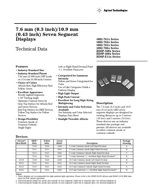
Features• Industry Standard Size • Industry Standard Pinout7.62 mm (0.300 inch) DIP Leads on 2.54 mm (0.100 inch) Centers • Choice of ColorsAlGaAs Red, High Efficiency Red,Yellow, Green• Excellent Appearance Evenly Lighted Segments ±50° Viewing AngleOptimum Contrast Given byGray Top Surface for AlGaAs Red and Green DevicesRed Top Surface for HER Devices Yellow Top Surface for Yellow Devices• Design Flexibility Common Anode or Common Cathode Single DigitsLeft or Right Hand Decimal Point ±1. Overflow Character• Categorized for Luminous IntensityYellow and Green Categorized for ColorUse of Like Categories Yields a Uniform Display • High Light Output • High Peak Current• Excellent for Long Digit String Multiplexing• Intensity and Color Selection AvailableSee Intensity and Color Selected Displays Data Sheet• Sunlight Viewable AlGaAsAlGaAs [1]HER [1]Yellow Green Package Red HDSP-5082-5082-HDSP-DescriptionDrawing7610762036007.6 mm Common Anode Left Hand Decimal A 7611762136017.6 mm Common Anode Right Hand Decimal B 7613762336037.6 mm Common Cathode Right Hand Decimal C 7616762636067.6 mm Universal ±1. Overflow Right Hand Decimal [2]D E15076507660460010.9 mm Common Anode Left Hand Decimal E E15176517661460110.9 mm Common Anode Right Hand Decimal F E15376537663460310.9 mm Common Cathode Right Hand Decimal G E15676567666460610.9 mm Universal ±1. Overflow Right Hand Decimal [2]HNotes:1. These displays are recommended for high ambient light operation. Please refer to the HDSP-E10X AlGaAs and HDSP-335X HER data sheet for low current operation.2. Universal pinout brings the anode and cathode of each segment’s LED out to separate pins. See internal diagram D.3. Universal pinout brings the anode and cathode of each segment’s LED out to separate pins. See internal diagram H.Devices5082-761x Series 5082-762x Series 5082-765x Series 5082-766x Series HDSP-360x Series HDSP-460x Series HDSP-E15x Series7.6 mm (0.3 inch)/10.9 mm (0.43 inch) Seven Segment Displays Technical DataDescriptionThe 7.6 mm (0.3 inch) and 10.9mm (0.43 inch) LED sevensegment displays are designed for viewing distances up to 3 metres (10 feet) and 5 metres (16 feet).These devices use an industry standard size package andpinouts. All devices are available as either common anode or common cathode.Part Numbering System5082 -X X X X-X X X X XHDSP-X X X X-X X X X XMechanical Options[1]00: No Mechanical OptionColor Bin Options[1,2]0: No Color Bin Limitation4: Color Bin 4 Only (applicable for Green devices only)B: Color Bins 2 and 3 (applicable for Yellow devices only)Maximum Intensity Bin[1,2]0: No Maximum Intensity Bin LimitationMinimum Intensity Bin[1,2]0: No Minimum Intensity Bin LimitationDevice Configuration/Color[1]0: Common Anode1: Common Anode3: Common CathodeDevice Specific Configuration[1]Refer to Respective DatasheetPackage[1]E: 10.9 mm (0.43 inch) Single Digit Seven Segment Display Notes:1. For codes not listed in the figure above, please refer to the respective datasheet or contact your nearestAgilent representative for details.2. Bin options refer to shippable bins for a part number. Color and Intensity Bins are typically restricted to 1bin per tube (exceptions may apply). Please refer to respective datasheet for specific bin limit information.displays are ideal for portable applications. The high light ambient displays are ideal for high light ambients or long string lengths. For additional informa-tion see the Low Current Seven Segment Displays, or High Light Ambient Seven Segment Displays data sheets.NOTES;1. DIMENSIONS IN MILLIMETRES AND (INCHES).2. ALL UNTOLERANCED DIMENSIONS ARE FOR REFERENCE ONLY.3. REDUNDANT ANODES.4. UNUSED DP POSITION.5. SEE INTERNALCIRCUIT DIAGRAM.6. REDUNDANT CATHODE.7. SEE PART NUMBER TABLE FOR L.H.D.P.AND R.H.D.P.DESIGNATION.8. FOR YELLOW AND GREEN DEVICES ONLY.Package DimensionsThese displays are ideal for most applications. Pin for pin equiva-lent displays are also available in a low current or high lightambient design. The low currentInternal Circuit DiagramAbsolute Maximum RatingsAlGaAs Red HER Yellow GreenHDSP-E1505082-7610/5082-7620/HDSP-3600/ Description Series7650 Series7660 Series4600 Series Units Average Power per Segment or DP9610580105mW Peak Forward Current per160[1]90[3]60[5]90[7]mA Segment or DPDC Forward Current per40[2]30[4]20[6]30[8]mA Segment or DPOperating Temperature Range-20 to +100[9]-40 to +100°C Storage Temperature Range -55 to +100°C Reverse Voltage per 3.0V Segment or DPWave Soldering Temperature for3 Seconds (1.59 mm [0.063 in.] 250°Cbelow Body)Notes:1.See Figure 1 to establish pulsed conditions.2. Derate above 46°C at 0.54 mA/°C.3. See Figure 6 to establish pulsed conditions.4. Derate above 53°C at 0.45 mA/°C.5. See Figure 7 to establish pulsed conditions.6. Derate above 81°C at 0.52 mA/°C.7. See Figure 8 to establish pulsed conditions.8. Derate above 39°C at 0.37 mA/°C.9. For operation below -20°C, contact your local Agilent components sales office or an authorized distributor.Electrical/Optical Characteristics at T A = 25°CAlGaAs RedDeviceSeries Parameter Symbol Min.Typ.Max.Units Test Conditions Luminous Intensity/Segment[1,2,5]I V8.515.0mcd I F = 20 mA(Digit Average)1.8V I F = 20 mAForward Voltage/Segment or DP V F2.03.0V I F = 100 mAHDSP-E15x Peak WavelengthλPEAK645nmDominant Wavelength[3]λd637nmReverse Voltage/Segment or DP[4]V R 3.015V I R = 100 µATemperature Coefficient of∆V F/°C-2mV/°CV F/Segment or DPThermal Resistance LED Junction-RθJ-PIN340°C/W/Segto-PinHigh Efficiency RedDeviceSeries Parameter Symbol Min.Typ.Max.Units Test Conditions 5082-761x Luminous Intensity/Segment[1,2,6]340800µcd I F = 5 mA (Digit Average)I V5082-765x3401115µcd I F = 5 mA Forward Voltage/Segment or DP V F 2.1 2.5V I F = 20 mAPeak WavelengthλPEAK635nmDominant Wavelength[3]λd626nm AllReverse Voltage/Segment or DP[4]V R 3.030V I R = 100 µATemperature Coefficient of∆V F/°C-2mV/°CV F/Segment or DPThermal Resistance LED RθJ-PIN280°C/WJunction-to-PinDevice Series ParameterSymbol Min.Typ.Max.Units Test Conditions 5082-762x Luminous Intensity/Segment [1,2]205620µcdI F = 5 mA(Digit Average)I V5082-766x290835µcd I F = 5 mA Forward Voltage/Segment or DP V F 2.2 2.5V I F = 20 mAPeak WavelengthλPEAK 583nm Dominant Wavelength [3,7]λd 581.5586592.5nm AllReverse Voltage/Segment or DP [4]V R 3.040V I R = 100 µA Temperature Coefficient of ∆V F /°C -2mV/°C V F /Segment or DP Thermal Resistance LED R θJ-PIN280°C/W/SegJunction-to-PinYellowNotes:1. Device case temperature is 25°C prior to the intensity measurement.2. The digits are categorized for luminous intensity. The intensity category is designated by a letter on the side of the package.3. The dominant wavelength, λd , is derived from the CIE chromaticity diagram and is that single wavelength which defines the color of the device.4. Typical specification for reference only. Do not exceed absolute maximum ratings.5. For low current operation, the AlGaAs HDSP-E10X series displays are recommended. They are tested at 1 mA dc/segment and are pin for pin compatible with the HDSP-E15X series.6. For low current operation, the HER HDSP-335X series displays are recommended. They are tested at 2 mA dc/segment and are pin for pin compatible with the 5082-7650 series.7. The Yellow (5082-7620/7660) and Green (HDSP-3600/4600) displays are categorized for dominant wavelength. The category is designated by a number adjacent to the luminous intensity category letter.High Performance GreenDevice Test Series ParameterSymbol Min.Typ.Max.Units Conditions HDSP-360x Luminous Intensity/Segment [1,2]8602700µcdI F = 10 mA(Digit Average)I VHDSP-460x10304000µcd I F = 10 mA Forward Voltage/Segment or DP V F 2.1 2.5V I F = 10 mAPeak WavelengthλPEAK 566nm Dominant Wavelength [3,7]λd 571577nm AllReverse Voltage/Segment or DP [4]V R 3.050V I R = 100 µA Temperature Coefficient of ∆V F /°C -2mV/°C V F /Segment or DP Thermal Resistance LED R θJ -PIN280°C/W/SegJunction-to-PinFigure 3. Forward Current vs. Forward Voltage.Figure 2. Maximum Allowable DC Current vs.Ambient Temperature.Figure 4. Relative Luminous Intensity vs. DC Forward Current.Figure 5. Relative Efficiency (Luminous Intensity per Unit Current) vs. Peak Current.AlGaAs RedI D C M A X . – M A X I M U M D C C U R R E N T P E R S E G M E N T – m AT A – AMBIENT TEMPERATURE – °C5030102051525354045I F – F O R W A R D C U R R E N T P E R S E G M E N T – m AV F – FORWARD VOLTAGE – V R E L A T I V E L U M I N O U S I N T E N S I T Y (N O R M A L I Z E D T O 1 A T 20 m A )0I F – FORWARD CURRENT PER SEGMENT – mA2.001.501.250.750.2520401.751.000.5010305152535ηP E A K – N O R M A L I Z E D R E L A T I V E EF F I C I E N C Y0.5I PEAK – PEAK FORWARD CURRENTPER SEGMENT – mA50.0150.05.0HER, Yellow, GreenFigure 8. Allowable Peak Current vs.Pulse Duration – Green Series.Figure 9. Maximum Allowable DC Current vs.Ambient Temperature.Figure 11. Relative LuminousIntensity vs. DC Forward Current.Figure 10. Forward Current vs.Forward Voltage.Figure 12. Relative LuminousEfficiency (Luminous Intensity per Unit Current) vs. Peak Current.HDSP-E15x IV Bin Category Min.Max.L 8.6715.90M 13.0023.80N 19.5035.80O 29.3053.60P 43.9080.50Intensity Bin Limits (mcd)AlGaAs RedHER5082-761x IV Bin Category Min.Max.B 0.3690.630C 0.5160.946D 0.774 1.418E 1.160 2.127F 1.740 3.190G 2.610 4.785H 3.9157.1775082-765xIV Bin Category Min.Max.B 0.3470.593C 0.4850.890D 0.728 1.333E 1.091 2.000F 1.636 3.000G 2.454 4.500H 3.6826.751Yellow5082-762x IV Bin Category Min.Max.B 0.2290.387C 0.3170.582D 0.4760.872E 0.714 1.311F 1.073 1.967G 1.609 2.950H 2.413 4.4255082-766xIV Bin Category Min.Max.C 0.2970.543D 0.4450.817E 0.669 1.225F 1.003 1.838G 1.504 2.758H 2.2564.137HDSP-460xIV Bin Category Min.Max.G 1.03 1.88H 1.54 2.82I 2.31 4.23J 3.46 6.34K 5.189.50L 7.7814.26GreenHDSP-360x IV Bin Category Min.Max.H 0.86 1.58I 1.29 2.37J 1.94 3.55K 2.90 5.33L 4.378.01Color CategoriesNote:All categories are established for classification of products. Products may not be available in all categories. Please contact your Agilent representatives for further clarification/information.Contrast EnhancementFor information on contrastenhancement, please seeApplication Note 1015.Soldering/CleaningFor information on solderingLEDs, please refer to ApplicationNote 1027.元器件交易网/semiconductorsFor product information and a complete list ofdistributors, please go to our web site.For technical assistance call:Americas/Canada: +1 (800) 235-0312 or(916) 788-6763Europe: +49 (0) 6441 92460China: 10800 650 0017Hong Kong: (+65) 6756 2394India, Australia, New Zealand: (+65) 6755 1939Japan: (+81 3) 3335-8152 (Domestic/Interna-tional), or 0120-61-1280 (Domestic Only)Korea: (+65) 6755 1989Singapore, Malaysia, Vietnam, Thailand,Philippines, Indonesia: (+65) 6755 2044Taiwan: (+65) 6755 1843Data subject to change.Copyright © 2004 Agilent Technologies, Inc.Obsoletes 5963-7394EJuly 17, 20045988-3325EN。
欧姆加温度计说明书
OMEGAHH501DKDigital ThermometerOMEGAnet On-Line Service Internet e-mail **************Servicing North America:USA: ISO 9001 Certified Canada:One Omega Drive, Box 4047976 Bergar Stamford, CT 06907-0047Laval (Quebec) H7L5A1 Tel: (203) 359-1660Tel: (514) 856-6928 FAX: (203)359-7700FAX: (514) 856-6886e-mail:**************e-mail:**************INTRODUCTIONThis instrument is a portable 3½ digit, compact-sized digital thermometer designed to use external K-type thermocouple as temperature sensor. Tem-perature indication follows Reference Temperature/Voltage Tables (N.I.S.T. Monograph 175 Revised to ITS-90) for K-type thermocouples.SAFETY INFORMATIONIt is recommended that you read the safety and operation instructions before using the thermometer.WARNINGTo avoid electrical shock, do not use this instrument when voltages at the measurement surface exceed 24V AC or DC.WARNINGTo avoid damage or burns, do not make temperaturemeasurement in microwave ovens.CAUTIONRepeated sharp flexing can break the thermocouple leads. To prolong lead life, avoid sharp bends in the leads, especially near the connector. The symbol on the instrument indicates that the operator must refer to an explanation in this manual.SPECIFICATIONSELECTRICALTemperature Scale: Celsius or Fahrenheit user-selectable Measurement Range: -50°C to 1300°C, (-58°F to 2000°F)Resolution: 1°C or 1°F, 0.1°C or 0.1°FAccuracy: Accuracy is specified for operating temperatures over the range of 18°C to 28°C (64°F to 82°F), for 1 year, not including thermocouple error.±(0.3% rdg + 1°C) -50°C to 1000°C±(0.5% rdg + 1°C) 1000°C to 1300°C±(0.3% rdg + 2°F) -58°F to 2000°FTemperature Coefficient: 0.1 times the applicable accuracy specification per °C from 0°C to 18°C and 28°C to 50°C (32°F to 64°F and 82°F to 122°F). Input Protection: 24V dc or 24V ac rms maximum input voltage on any combination of input pins.Reading Rate: 2.5 times per second.Input Connector: Accepts standard miniature thermocouple connectors (flat blades spaced 7.9mm, center to center).ENVIRONMENTALAmbient Operating Ranges: 0°C to 50°C (32°F to 122°F) <80% R.H. Storage Temperature: -20°C to 60°C (-4°F to 140°F) <70% R.H. GENERALDisplay: 3½ digit liquid crystal display (LCD) with maximum reading of 1999. Battery: Standard 9V battery.Battery Life: 200 hours typical with carbon zinc battery.Dimensions: 192mm(H) x 91mm(W) x 52.5mm(D).Weight: 365g.OPERATING INSTRUCTIONSSelecting the Temperature ScaleReadings are displayed in either degrees Celsius(°C) or degrees Fahrenheit(°F). To change the temperature scale, press the "°C" or "°F"key.Selecting the Display ResolutionThe thermometer allows two choices of resolution:High resolution: 0.1°C or 0.1°FLow resolution: 1.0°C or 1.0°FTo select the alternate display resolution, press the corresponding "0.1°/1°" key.HOLD ModeDisplay Back-LightPressing the "" key to toggle turn on or turn off the Back-Light.MAX ModePressing the Max key to enter the MAX mode. The thermometer then records and updates the maximum absolute values and the MAX annunciator appears on the display. Pressing the MAX key again to exit the MAX recording mode. In the MAX mode, press HOLD key to stop the recording, press HOLD again to resume recording.T1,T2,T3,T4, T1-T2,T1-T3,T1-T4 Temperature Measurement1. The function switch indicates which input is selected for display; T1 thermocouple, T2 thermocouple,T3 thermocoupleor, T4 thermocouple or the difference between the two thermocouples (T1-T2, T1-T3, T1-T4).2. Connect a type k thermocouple to the jack on the instrument. Place the probe or thermocouple tip on or in the material to be measured and take the temperature reading directly from the display.MAINTENANCEWARNINGTo avoid possible electrical shock, disconnect the thermocoupleconnectors from the thermometer before removing the cover. Battery ReplacementPower is supplied by a 9 volt "transistor" battery. (NEDA 1604, IEC 6F22). The " " appears on the LCD display when replacement is needed. To replace the battery, remove the two screws from the back of the meter and lift off the battery cover. Remove the battery from battery contacts.HH501DK CALIBRATION PROCEDURENote: The following calibration procedure should perform only by qualified technicians who have access to the items as following.Equipment: The class of calibrator had better 10 times greater than the measured meter. Temperature CalibrationInsert the K type thermocouple to the female connector, and the other side of this probe to Temperature Calibrator and connect output to the voltage meter. We must allow the K type to stabilize for at least 1 minute and make sure “+” and “-“polarity is right position.1. Set the range to the T1/0.1°C, and then apply 0°C to T1 input (T2 input open)adjust R3 and R4 (fine adj.) until LCD reading reads 0.0±0.1°C.2. Set the range to the T2/0.1°C, and then Apply 0°C to T2 input (T1 input open)adjust R1 and R2 (fine adj.) until LCD reading reads 0.0±0.1°C.3. Set the range to the T1/0.1°F, and then apply 0°F to T1 input (T2 input open)adjust R6 until LCD reading reads 0.0±0.1°F.4. Set the range to the T1/0.1°F, and then apply 165°F to T1 input (T2 inputopen) adjust R7 until LCD reading reads 165.0±0.1°F.5. Set the range to the T1/1°F, and then apply 1832°F to T1 input (T2 inputopen) adjust R5 until LCD reading reads 1832±1°F.6. Set the range to the T1/1°C, and then apply 1000°C to T1 input (T2 inputopen) adjust R8 until LCD reading reads 1000±0°C.WARRANTY / DISCLAIMEROMEGA ENGINEERING, INC. warrants this unit to be free of defects in materials and workmanship for a period of 13 months from date of purchase. OMEGA Warranty adds an additional one (1) month grace period to the normal one (1) year product warranty to cover handling and shipping time. This ensures that OMEGA's customers receive maximum coverage on each product.If the unit should malfunction, it must be returned to the factory for evaluation. OMEGA's Customer Service Department will issue an Authorized Return (AR) number immediately upon phone or written request. Upon examination by OMEGA, if the unit is found to be defective it will be repaired or replaced at no charge. OMEGA's WARRANTY does not apply to defects resulting from any action of the purchaser, including but not limited to mishandling, improper interfacing, operation outside of design limits, improper repair, or unauthorized modification. This WARRANTY is VOID if the unit shows evidence of having been tampered with or shows evidence of being damaged as a result of excessive corrosion; or current, heat moisture or vibration; improper specification; misapplication; misuse or other operating conditions outside of OMEGA's control. Components which wear are not warranted, including but not limited to contact points, fuses, and triacs.OMEGA is pleased to offer suggestions on the use of its various products. However, OMEGA neither assumes responsibility for any omissions or errors nor assumes liability for any damages that result from the use of its products in accordance with information provided by OMEGA, either verbal or written. OMEGA warrants only that the parts manufactured by it will be as specified and free of defects. OMEGA MAKES NO OTHER WARRANTIES OR REPRESENTATIONS OF ANY KIND WHATSOEVER, EXPRESSED OR IMPLIED, EXCEPT THAT OF TITLE AND ALL IMPLIED WARRANTIES INCLUDING ANY WARRANTY OF MERCHANTABILITY AND FITNESS FOR A PARTICULAR PURPOSE ARE HEREBY DISCLAIMED. LIMITATION OF LIABILITY: The remedies of purchaser set forth herein are exclusive and the total liability of OMEGA with respect to this order, whether based on contract, warranty, negligence, indemnification, strict liability or otherwise, shall not exceed the purchase price of the component upon which liability is based. In no event shall OMEGA be liable for consequential, incidental or special damages.CONDITIONS: Equipment sold by OMEGA is not intended to be used, nor shall it be used: (1) as a "Basic Component" under 10 CFR 21 (NRC), used in or with any nuclear installation or activity; or (2) in medical applications or used on humans. Should any Product(s) be used in or with any nuclear installation or activity, medical application, used on humans, or misused in any way, OMEGA assumes no responsibility as set forth in our basic WARRANTY / DISCLAIMER language, and additionally, purchaser will indemnify OMEGA and hold OMEGA harmless from any liability or damage whatsoever arising out of the use of the Product(s) in such a manner.RETURN REQUESTS / INQUIRIESDirect all warranty and repair requests/inquiries to the OMEGA Customer Service Department. BEFORE RETURNING ANY PRODUCT(S) TO OMEGA, PURCHASER MUST OBT AIN AN AUTHORIZED RETURN (AR) NUMBER FROM OMEGA'S CUSTOMER SERVICE DEP ARTMENT (IN ORDER TO AVOID PROCESSING DELAYS). The assigned AR number should then be marked on the outside of the return package and on any correspondence.The purchaser is responsible for shipping charges, freight, insurance and proper packaging to prevent breakage in transit.FOR WARRANTY RETURNS, please have the following information available BEFORE contacting OMEGA:1.P.O. number under which the product was PURCHASED.2.Model and serial number of the product under warranty, and3.Repair instructions and/or specific problems relative to theproduct.FOR NON-WARRANTY REPAIRS, consult OMEGA for current repair charges. Have the following informationavailable BEFORE contacting OMEGA:1.P.O. number to cover the COST of the repair.2.Model and serial number of product , and3.Repair instructions and/or specific problems relative to theproduct.OMEGA's policy is to make running changes, not model changes, whenever an improvement is possible. This affords our customers the latest in technology and engineering. OMEGA is a registered trademark of OMEGA ENGINEERING, INC. © Copyright 1999 OMEGA ENGINEERING,Where Do I Find Everything I Need for Process Measurement and Control?OMEGA...Of Course!TEMPERATUREþThermocouple, RTD & Thermistor Probes, Connectors, Panels & Assemblies þWire: Thermocouple, RTD & Thermistor þCalibrators & Ice Point ReferencesþRecorders, Controllers & Process Monitors þInfrared PyrometersPRESSURE/STRAIN AND FORCEþTransducers & Strain GaugesþLoad Cells & Pressure GaugesþDisplacement TransducersþInstrumentation & AccessoriesFLOW/LEVELþRotameters, Gas Mass Flowmeters& Flow ComputersþAir Velocity IndicatorsþTurbine/Paddlewheel SystemsþTotalizers & Batch ControllerspH/CONDUCTIVITYþpH Electrodes, Testers & AccessoriesþBenchtop/Laboratory MetersþControllers, Calibrators, Simulators& PumpsþIndustrial pH & Conductivity Equipment DATA ACQUISITIONþData Acquisition &Engineering SoftwareþCommunications-Based Acquisition SystemsþPlug-in Cards for Apple, IBM& CompatiblesþDatalogging SystemsþRecorders, Printers & Plotters HEATERSþHeating CableþCartridge & Strip HeatersþImmersion & Band HeatersþFlexible HeatersþLaboratory Heaters ENVIRONMENTAL MONITORING AND CONTROL þMetering & Control Instrumentation þRefractometersþPumps & TubingþAir, Soil & Water MonitorsþIndustrial Water & Wastewater TreatmentþpH, Conductivity & Dissolved Oxygen InstrumentsM-2985/0799。
5082-511E-LL000中文资料
DescriptionThis 14.22 mm (0.56 inch) LED seven-segment display uses industry standard size package and pinout.The device is available in eithercommon anode or common cathode.Agilent HDSP-511x/513x14.22 mm (0.56 inch) General Purpose Seven-Segment DisplayData SheetFeatures•Industry standard size •Industry standard pinout 14.22 mm (0.56 inch)DIP lead on 2.54 mm •Choice of colorsHigh Efficiency Red (HER), Green,AlGaAs Red, and Yellow •Excellent appearanceEvenly lighted segments gray package gives optimum contrast ± 50° viewing angle •Design flexibilityCommon anode or common cathode Single digitLeft and right hand decimal point•Categorized for luminous intensityGreen and yellow categorized for color Applications•Suitable for indoor use•Not recommended for industrial application, i.e., operating tem-perature requirements exceeding +85˚C or below –25˚C [1]•Extreme temperature cycling not recommendedNotes:1.For additional details, please contact your local Agilent sales office or an authorized distributor.Devices HERGreenAlGaAs Red Yellow DescriptionHDSP-511E HDSP-511G HDSP-511A HDSP-511Y Common Anode, Right Hand Decimal HDSP-513EHDSP-513GHDSP-513AHDSP-513YCommon Cathode, Right Hand DecimalThe choice of colors includes High Efficiency Red (HER),Green, AlGaAs Red, and Yellow.The gray face displays aresuitable for indoor use.Part Numbering SystemNotes:1. For codes not listed in the figure above, please refer to the respective datasheet or contact your nearest Agilent representative for details.2. Bin options refer to shippable bins for a part number. Color and Intensity Bins are typically restricted to 1bin per tube (exceptions may apply). Please refer to respective datasheet for specific bin limit information.5082 -X X X X-X X X X X HDSP-X X X X-X X X X XMechanical Options [1]00: No Mechanical Option Color Bin Options [1,2]0: No Color Bin LimitationMaximum Intensity Bin [1,2]0: No Maximum Intensity Bin Limitation Minimum Intensity Bin [1,2]0: No Minimum Intensity Bin Limitation Device Configuration/Color [1]A: AlGaAs RedE: High Efficiency Red G: Green Y: YellowDevice Specific Configuration [1]Refer to Respective Datasheet Package [1]Refer to Respective DatasheetInternal Circuit DiagramPackage Dimensions0.50 ± 0.05 TYP. 10 PLACESTOP END VIEWFRONT VIEW SIDE VIEWALL DIMENSIONS ARE IN MILLIMETERS (INCHES).COMMON CATHODECOMMON ANODE COMMON ANODECOMMON CATHODEPINFUNCTIONPIN 1CATHODE e 2CATHODE d3COMMON ANODE 4CATHODE c 5CATHODE DP 6CATHODE b 7CATHODE a8COMMON ANODE 9CATHODE f 10CATHODE g12345678910FUNCTIONANODE e ANODE dCOMMON CATHODE ANODE c ANODE DPANODE b ANODE aCOMMON CATHODE ANODE f ANODE gHDSP-511E/511G/511Y/511AHDSP-513E/513G/513Y/513AGreen Device HDSP-ParameterSymbol Min.Typ.Max.Units Test Conditions Luminous Intensity/Segment I V 2.001 4.100mcd I F = 10 mA Forward Voltage V F 2.06V I F = 10 mA 1.802.25 2.60V I F = 20 mAPeak Wavelength λPEAK 568nm Dominant Wavelength λd 573nm Reverse VoltageVR5VI R = 100 µA511G 513GAbsolute Maximum Ratings at T A = 25˚C HERGreenAlGaAs Red Yellow DescriptionHDSP-51xE HDSP-51xG HDSP-51xA HDSP-51xY Units Power Dissipation Segment 60653052mW Forward Current Segment25[1]25[2]15[3]20[4]mA Peak Forward Current per Segment 1001008080mA (1/10 Duty Factor at 10 KHz)Operating Temperature Range –35 to +85–35 to +85–35 to +85–35 to +85˚C Storage Temperature Range–35 to +85–35 to +85–35 to +85–35 to +85˚C Reverse Voltage per Segment or DP5555V Wavesoldering Temperature for 3 seconds 250250250250˚C(at 2 mm Distance from the body)Notes:1.Derate above 25˚C at 0.33 mA/˚C.2.Derate above 25˚C at 0.33 mA/˚C.3.Derate above 25˚C at 0.2 mA/˚C.4.Derate above 25˚C at 0.27 mA/˚C.Electrical/Optical Characteristics at T A = 25˚C High Efficiency Red (HER)Device HDSP-ParameterSymbol Min.Typ.Max.Units Test Conditions Luminous Intensity/Segment I V 1.73mcd I F = 5 mA 2.0014.100mcd I F = 10 mA Forward Voltage V F 2.05 2.40V I F = 20 mAPeak Wavelength λPEAK 635nm Dominant Wavelength λd 620nm Reverse VoltageVR5VI R = 100 µA511E 513EColor Bin Limits (nm at 10 mA)Dominant Wavelength (nm)Color Bin Min.Max.Note:1.Tolerance for each bin limit is 1 nm.Yellow Device HDSP-ParameterSymbolMin.Typ.Max.Units Test Conditions Luminous Intensity/Segment I V 1.03mcd I F = 5 mA 1.2512.600mcd I F = 10 mA Forward Voltage V F 2.15 2.60V I F = 20 mAPeak Wavelength λPEAK 595nm Dominant Wavelength λd 590nm Reverse VoltageVR5VI R = 100 µA511Y 513YAlGaAs Red Device HDSP-ParameterSymbol Min.Typ.Max.Units Test Conditions Luminous Intensity/Segment I V 4.93mcd I F = 5 mA 3.2016.500mcd I F = 10 mA Forward Voltage V F 1.85 2.00V I F = 20 mAPeak Wavelength λPEAK 660nm Dominant Wavelength λd 643nm Reverse VoltageVR5VI R = 100 µA511A 513AIntensity Bin Limits (mcd at 10 mA)Bin HER/Green Yellow AlGaAs Red Name Min.[1]Max.[1]Min.[1]Max.[1]Min.[1]Max.[1]H NA NA 1.251 2.000NA NA I 2.001 3.200 2.001 3.200NA NA J 3.201 5.050 3.201 5.050 3.201 5.050K 5.0518.000NA NA 5.0518.000LNANANANA8.00112.650Note:1.Tolerance for each bin limit is ± 10%.Figure 1. Maximum allowable average or DC current vs. ambient temperature.Figure 2. Forward current vs. forward voltage.Figure 3. Relative luminous intensity vs. DC forward current.High Efficiency Red (HER)Figure 4. Relative efficiency (luminousintensity per unit current) vs. peak current.30T A – AMBIENT TEMPERATURE – °CM A X I M U M D C C U R R E N T P E R S E G M E N T – m AV F – FORWARD VOLTAGE – VI F – F O R W A R D C U R R E N T P E R S E G M E N T – m AR E L A T I V E E F F I C I E N C Y (N O R M A L I Z E D T O 1 A T 10 m A )1.4005101520253035404550I PEAK – PEAK FORWARD CURRENTPER SEGMENT – mA 0.20.40.60.81.01.2R E L A T I V E E F F I C I E N C Y (N O R M A L I Z E D T O 1 A T 10 m A )1.4005101520253035404550I PEAK – PEAK FORWARD CURRENTPER SEGMENT – mA0.20.40.60.81.01.2Figure 7. Relative luminous intensity vs. DC forward current.Figure 8. Relative efficiency (luminous intensity per unit current) vs. peak current.Figure 5. Maximum allowable average or DC current vs. ambient temperature.Figure 6. Forward current vs. forward voltage.Green302520151050020*********T A – AMBIENT TEMPERATURE – °CM A X I M U M D C C U R R E N T P E R S E G M E N T – m AV F – FORWARD VOLTAGE – VI F – F O R W A R D C U R R E N T P E R S E G M E N T – m A3.52.52.01.51.00.50051015202530I F – FORWARD CURRENT FOR SEGMENT – mAR E L A T I V E L U M I N O U S I N T E N S I T Y (N O R M A L I Z E D T O 1 A T 10 m A )353.0R E L A T I V E E F F I C I E N C Y (N O R M A L I Z E D T O 1 A T 10 m A )05101520253035404550I PEAK – PEAK FORWARD CURRENTPER SEGMENT – mA0.20.40.60.81.01.2Figure 9. Maximum allowable average or DC current vs. ambient temperature.Figure 10. Forward current vs. forward voltage.Figure 11. Relative luminous intensity vs. DC forward current.Figure 12. Relative efficiency (luminous intensity per unit current) vs. peak current.AlGaAs RedT A – AMBIENT TEMPERATURE – °CM A X I M U M D C C U R R E N T P E R S E G M E N T – m AV F – FORWARD VOLTAGE – VI F – F O R W A R D C U R R E N T P E R S E G M E N T – m A3.02.52.01.51.00.5051015202530I F – FORWARD CURRENT FOR SEGMENT – mAR E L A T I V E L U M I N O U S I N T E N S I T Y (N O R M A L I Z E D T O 1 A T 10 m A )35R E L A T I V E E F F I C I E N C Y (N O R M A L I Z E D T O 1 A T 10 m A )05101520253035404550I PEAK – PEAK FORWARD CURRENTPER SEGMENT – mA0.20.40.60.81.01.2Figure 13. Maximum allowable average or DC current vs. ambient temperature.Figure 14. Forward current vs. forward voltage.Figure 15. Relative luminous intensity vs. DC forward current.Figure 16. Relative efficiency (luminous intensity per unit current) vs. peak current.Yellow252015105T A – AMBIENT TEMPERATURE – °CM A X I M U M D C C U R R E N T P E R S E G M E N T – m A3.52.52.01.51.00.50051015202530I F – FORWARD CURRENT FOR SEGMENT – mAR E L A T I V E L U M I N O U S I N T E N S I T Y (N O R M A L I Z E D T O 1 A T 10 m A )353.0R E L A T I V E E F F I C I E N C Y (N O R M A L I Z E D T O 1 A T 10 m A )1.4005101520253035404550I PEAK – PEAK FORWARD CURRENTPER SEGMENT– mA0.20.40.60.81.01.2V F – FORWARD VOLTAGE – VI F – F O R W A R D C U R R E N T P E R S E G M E N T – m A/semiconduc-torsFor product information and a complete list of distributors, please go to our web site.For technical assistance call:Americas/Canada: +1 (800) 235-0312 or (916) 788-6763Europe: +49 (0) 6441 92460China: 10800 650 0017Hong Kong: (+65) 6756 2394India, Australia, New Zealand: (+65) 6755 1939 Japan: (+81 3) 3335-8152(Domestic/ International), or 0120-61-1280(Domestic Only) Korea: (+65) 6755 1989Singapore, Malaysia, Vietnam, Thailand, Philippines, Indonesia: (+65) 6755 2044 Taiwan: (+65) 6755 1843Data subject to change.Obsoletes 5980-2919ENJune 30, 20045988-2968EN。
2021年各种液位计说明介绍模板

公司简介欧阳光明(2021.03.07)北京铁强科技发展有限公司,位于我们伟大的首都——北京,是一家以工程仪表生产、研发为主的科技型企业,是一个极具活力与前景的多元化的新型民营企业。
公司技术力量雄厚,依靠北京的人才、技术、信息等优势,自2000年成立以来,通过短短七年多时间,就在仪器仪表生产制造领域内谱写一个又一个神话。
公司先后与北仪集团、德国西门子公司、美国麦克公司等仪表生产制造商进行广泛而深入的合作,在合作中公司产品的品质和质量得到很大提升。
同时,公司也在积极借鉴和引进国外先进技术和生产工艺,产品的科技含量不断提高、种类也在不断丰富。
另外,公司不断以新技术、新工艺、新材料、新设计理念设计生产品质高、性能优、用途广、使用寿命长的产品。
公司自主生产磁翻柱液位计、浮球液位计(液位开关)、钢带液位计、磁致伸缩液位计、微波物位计、电容式液位计、超声波液位计、音叉物位开关、电容式物位计、差压变送器等物位测量仪表。
同时,公司还经营流量仪表、压力仪表、温度仪表以及成分分析仪表等自动化测量、控制仪表。
经过几年的努力,公司发展了一支专业化、国际化、规模化的研发、生产、和管理团队。
公司现有员工100余名,其中有高级职称的技术人员5人、大专及以上各类专业人才80余名。
是“中国石化物资资源市场成员”单位;是“中国石油天然气集团公司一级供应网络”单位。
是众多国内外用户的高品质、可信赖的工业计量器具服务商。
公司一直秉承“技术为本,质量为先,笃信予人,益精致远”的经营理念,以“更强、更大、更实”为经营宗旨,开拓进取,务实创新,在做好产品生产和经营的基础上,还以打造中国仪表名牌为己任,投资开发有自主知识产权的产品。
在发展过程中,公司始终以快速的反应、精湛的技艺、热忱的服务及时为用户排忧解难,也因此得到了广大用户与社会各界的一致认可。
如今,公司全体员工正走专业化、特色化、精细化经营之道,并朝着两年时间内年销售额翻两番的目标奋力前进!北京铁强仪表科技发展有限公司产品选型样本目录01、磁翻柱液位计 (3)02、浮球液位计(液位开关) (5)03、防爆浮球液位开关 (7)04、玻璃板式液位计 (8)05、玻璃管式液位计 (10)06、钢带液位计 (12)07、重锤探测液位计 (14)08、超声波物位计 (15)09、智能雷达液位计 (17)10、导波雷达液位计 (19)11、电容式液位计 (21)12、射频导纳物位控制器 (23)13、音叉物位控制器 (25)14、磁致伸缩物位计 (27)15、压力液位变送器 (29)16、小型浮球液位计(液位开关) (31)17、常用客户名单 (32)注:我们是一家专业生产物位仪器仪表的科技型公司,随着市场的需求变化、我们的技术人员也会在保证质量的前提下,对产品进行改进,改造后的产品外观会有所变化、性能也会有所提高。
5082-A907-O0000中文资料
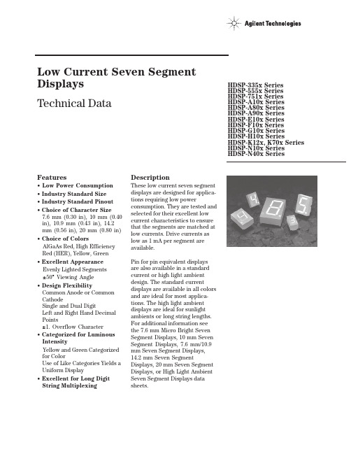
Features• Low Power Consumption • Industry Standard Size• Industry Standard Pinout • Choice of Character Size7.6 mm (0.30 in), 10 mm (0.40 in), 10.9 mm (0.43 in), 14.2 mm (0.56 in), 20 mm (0.80 in)• Choice of ColorsAlGaAs Red, High Efficiency Red (HER), Yellow, Green• Excellent Appearance Evenly Lighted Segments±50° Viewing Angle• Design FlexibilityCommon Anode or Common CathodeSingle and Dual DigitLeft and Right Hand Decimal Points±1. Overflow Character• Categorized for Luminous IntensityYellow and Green Categorized for ColorUse of Like Categories Yields a Uniform Display• Excellent for Long Digit String Multiplexing DescriptionThese low current seven segment displays are designed for applica-tions requiring low power consumption. They are tested and selected for their excellent low current characteristics to ensure that the segments are matched at low currents. Drive currents as low as 1 mA per segment are available.Pin for pin equivalent displays are also available in a standard current or high light ambient design. The standard current displays are available in all colors and are ideal for most applica-tions. The high light ambient displays are ideal for sunlight ambients or long string lengths. For additional information see the 7.6 mm Micro Bright Seven Segment Displays, 10 mm Seven Segment Displays, 7.6 mm/10.9 mm Seven Segment Displays, 14.2 mm Seven Segment Displays, 20 mm Seven Segment Displays, or High Light Ambient Seven Segment Displays data sheets.Low Current Seven SegmentDisplays Technical Data HDSP-335x SeriesHDSP-555x SeriesHDSP-751x SeriesHDSP-A10x Series HDSP-A80x Series HDSP-A90x Series HDSP-E10x Series HDSP-F10x Series HDSP-G10x Series HDSP-H10x Series HDSP-K12x, K70x Series HDSP-N10x SeriesHDSP-N40x SeriesDevicesAlGaAs HER Yellow Green Package HDSP-HDSP-HDSP-HDSP-Description Drawing A1017511A801A9017.6 mm Common Anode Right Hand Decimal A A1037513A803A9037.6 mm Common Cathode Right Hand Decimal B A1077517A807A9077.6 mm Common Anode ±1. Overflow C A1087518A808A9087.6 mm Common Cathode ±1. Overflow D F10110 mm Common Anode Right Hand Decimal E F10310 mm Common Cathode Right Hand Decimal F F10710 mm Common Anode ±1. Overflow G F10810 mm Common Cathode ±1. Overflow H G10110 mm Two Digit Common Anode Right Hand Decimal X G10310 mm Two Digit Common Cathode Right Hand Decimal Y E100335010.9 mm Common Anode Left Hand Decimal I E101335110.9 mm Common Anode Right Hand Decimal J E103335310.9 mm Common Cathode Right Hand Decimal K E106335610.9 mm Universal ±1. Overflow[1]L H101555114.2 mm Common Anode Right Hand Decimal M H103555314.2 mm Common Cathode Right Hand Decimal N H107555714.2 mm Common Anode ±1. Overflow O H108555814.2 mm Common Cathode ±1. Overflow P K121K70114.2 mm Two Digit Common Anode Right Hand Decimal R K123K70314.2 mm Two Digit Common Cathode Right Hand Decimal S N10020 mm Common Anode Left Hand Decimal Q N101N40120 mm Common Anode Right Hand Decimal T N103N40320 mm Common Cathode Right Hand Decimal U N10520 mm Common Cathode Left Hand Decimal V N106N40620 mm Universal ±1. Overflow[1]W Note:1. Universal pinout brings the anode and cathode of each segment’s LED out to separate pins. See internal diagrams L or W.Part Numbering System5082-x xx x-x x x xxHDSP-x xx x-x x x xxMechanical Options[1]00: No mechanical optionColor Bin Options[1,2]0: No color bin limitationMaximum Intensity Bin[1,2]0: No maximum intensity bin limitationMinimum Intensity Bin[1,2]0: No minimum intensity bin limitationDevice Configuration/Color[1]G: GreenDevice Specific Configuration[1]Refer to respective datasheetPackage[1]Refer to Respective datasheetNotes:1. For codes not listed in the figure above, please refer to the respective datasheet or contact your nearest Agilent representative fordetails.2. Bin options refer to shippable bins for a part-number. Color and Intensity Bins are typically restricted to 1 bin per tube (excep-tions may apply). Please refer to respective datasheet for specific bin limit information.Package DimensionsPackage Dimensions (cont.)Package Dimensions (cont.)*The Side View of package indicates Country of Origin.Package Dimensions (cont.)Package Dimensions (cont.)Package Dimensions (cont.)Internal Circuit DiagramInternal Circuit Diagram (cont.)Absolute Maximum RatingsAlGaAs Red - HDSP-HERA10X/E10X/H10X HDSP-751X/Yellow GreenK12X/N10X/N40X335X/555X/HDSP-A80X HDSP-A90X Description F10X, G10X Series K70X Series Series Series Units Average Power per Segment or DP375264mW Peak Forward Current per 45mA Segment or DPDC Forward Current per15[1]15[2]mA Segment or DPOperating Temperature Range-20 to +100-40 to +100°C Storage Temperature Range -55 to +100°C Reverse Voltage per Segment 3.0V or DPWave Soldering Temperature for 3Seconds (1.60 mm [0.063 in.] below 250°C seating body)Notes:1. Derate above 91°C at 0.53 mA/°C.2. Derate HER/Yellow above 80°C at 0.38 mA/°C and Green above 71°C at 0.31 mA/°C.Electrical/Optical Characteristics at T A = 25°CAlGaAs RedDeviceSeriesHDSP-Parameter Symbol Min.Typ.Max.Units Test Conditions315600I F = 1 mA A10x3600I F = 5 mA330650I F = 1 mAF10x, G10x3900I F = 5 mA390650I F = 1 mA E10x Luminous Intensity/Segment[1,2]I Vµcd(Digit Average)3900I F = 5 mA400700I F = 1 mAH10x, K12x4200I F = 5 mA270590I F = 1 mAN10x, N40x3500I F = 5 mA1.6I F = 1 mAForward Voltage/Segment or DP V F 1.7V I F = 5 mA1.82.2I F = 20 mA PkAll Devices Peak WavelengthλPEAK645nmDominant Wavelength[3]λd637nmReverse Voltage/Segment or DP[4]V R 3.015V I R = 100 µATemperature Coefficient of∆V F/°C-2 mV mV/°CV F/Segment or DPA10x255F10x, G10x320E10x340Thermal Resistance LED RθJ-PIN°C/W/SegH10x, K12x Junction-to-Pin400N10x, N40x430High Efficiency RedDeviceSeriesHDSP-Parameter Symbol Min.Typ.Max.Units Test Conditions160270I F = 2 mA 751x1050I F = 5 mA200300I F = 2 mA Luminous Intensity/Segment[1,2]I V mcd(Digit Average)1200I F = 5 mA335x, 555x,K70x270370I F = 2 mA1480I F = 5 mA1.6I F = 2 mAForward Voltage/Segment or DP V F 1.7V I F = 5 mA2.1 2.5I F = 20 mA Pk All Devices Peak WavelengthλPEAK635nmDominant Wavelength[3]λd626nmReverse Voltage/Segment or DP[4]V R 3.030V I R = 100 µATemperature Coefficient of∆V F/°C-2mV/°CV F/Segment or DP751x200335x Thermal Resistance LED RθJ-PIN280°C/WJunction-to-Pin555x, K70x345YellowDeviceSeriesHDSP-Parameter Symbol Min.Typ.Max.Units Test Conditions Luminous Intensity/Segment[1,2]250420I F = 4 mA(Digit Average)I V mcd1300I F = 10 mA1.7I F = 4 mAForward Voltage/Segment or DP V F 1.8V I F = 5 mA A80x2.1 2.5I F = 20 mA PkPeak WavelengthλPEAK583nmDominant Wavelength[3,5]λd581.5585592.5nmReverse Voltage/Segment or DP[4]V R 3.030V I R = 100 µATemperature Coefficient of∆V F/°C-2mV/°CV F/Segment or DPThermal Resistance LED RθJ-PIN200°C/WJunction-to-PinGreenDeviceSeriesHDSP-Parameter Symbol Min.Typ.Max.Units Test Conditions Luminous Intensity/Segment[1,2]250475I F = 4 mA(Digit Average)I V mcd1500I F = 10 mA1.9I F = 4 mAForward Voltage/Segment or DP V F 2.0V I F = 10 mA A90x2.1 2.5I F = 20 mA PkPeak WavelengthλPEAK566nmDominant Wavelength[3,5]λd571577nmReverse Voltage/Segment or DP[4]V R 3.030V I R = 100 µATemperature Coefficient of∆V F/°C-2mV/°CV F/Segment or DPThermal Resistance LED RθJ-PIN200°C/WJunction-to-PinNotes:1. Device case temperature is 25°C prior to the intensity measurement.2. The digits are categorized for luminous intensity. The intensity category is designated by a letter on the side of the package.3. The dominant wavelength, λd, is derived from the CIE chromaticity diagram and is the single wavelength which defines the color of thedevice.4. Typical specification for reference only. Do not exceed absolute maximum ratings.5. The yellow (HDSP-A800) and Green (HDSP-A900) displays are categorized for dominant wavelength. The category is designated by anumber adjacent to the luminous intensity category letter.AlGaAs RedIntensity Bin Limits (mcd)AlGaAs RedHDSP-A10xIV Bin Category Min.Max.E0.3150.520F0.4280.759G0.621 1.16H0.945 1.71I 1.40 2.56J 2.10 3.84K 3.14 5.75L 4.708.55HDSP-E10x/F10x/G10xIV Bin Category Min.Max.D0.3910.650E0.5320.923F0.755 1.39G 1.13 2.08H 1.70 3.14HDSP-H10x/K12xIV Bin Category Min.Max.C0.4150.690D0.5650.990E0.810 1.50F 1.20 2.20G 1.80 3.30H 2.73 5.00I 4.097.50HDSP-N10xIV Bin Category Min.Max.A0.2700.400B0.3250.500C0.4150.690D0.5650.990E0.810 1.50F 1.20 2.20G 1.80 3.30H 2.73 5.00I 4.097.50Intensity Bin Limits (mcd), continued HERHDSP-751xIV Bin Category Min.Max.B0.1600.240C0.2000.300D0.2500.385E0.3150.520F0.4280.759G0.621 1.16HDSP-751xIV Bin Category Min.Max.B0.2400.366C0.3000.477D0.3910.650E0.5320.923F0.755 1.39G 1.13 2.08H 1.70 3.14HDSP-555x/K70xIV Bin Category Min.Max.A0.2700.400B0.3250.500C0.4150.690D0.5650.990E0.810 1.50F 1.20 2.20G 1.80 3.30H 2.73 5.00I 4.097.50Intensity Bin Limits (mcd), continued YellowHDSP-A80xIV Bin Category Min.Max.D0.2500.385E0.3150.520F0.4250.760G0.625 1.14H0.940 1.70I 1.40 2.56J 2.10 3.84K 3.14 5.76L 4.718.64M7.0713.00N10.6019.40O15.9029.20P23.9043.80Q35.8065.60GreenHDSP-A90xIV Bin Category Min.Max.E0.3150.520F0.4250.760G0.625 1.14H0.940 1.70I 1.40 2.56J 2.10 3.84K 3.14 5.76L 4.718.64M7.0713.00N10.6019.40O15.9029.20P23.9043.80Q35.8065.60Electrical/OpticalFor more information on electrical/optical characteristics, please see Application Note 1005.Contrast Enhancement For information on contrast enhancement, please see Application Note 1015.Soldering/Cleaning Cleaning agents from the ketone family (acetone, methyl ethyl ketone, etc.) and from the chorinated hydrocarbon family (methylene chloride, trichloro-ethylene, carbon tetrachloride, etc.) are not recommended for cleaning LED parts. All of these various solvents attack or dissolve the encapsulating epoxies used to form the package of plastic LED parts.For information on soldering LEDs, please refer to Application Note 1027.Note:All categories are established for classification of products. Productsmay not be available in all categories. Please contact your localAgilent representatives for further clarification/information.Color Categories/semiconductorsFor product information and a complete list ofdistributors, please go to our web site.For technical assistance call:Americas/Canada: +1 (800) 235-0312 or(916) 788 6763Europe: +49 (0) 6441 92460China: 10800 650 0017Hong Kong: (+65) 6271 2451India, Australia, New Zealand: (+65) 6271 2394Japan: (+81 3) 3335-8152(Domestic/International), or0120-61-1280(Domestic Only)Korea: (+65) 6271 2194Malaysia, Singapore: (+65) 6271 2054Taiwan: (+65) 6271 2654Data subject to change.Copyright © 2005 Agilent Technologies, Inc.Obsoletes 5988-8412ENJanuary 19, 20055989-0080EN。
HP5082-7740中文资料

Features• Industry Standard Size • Industry Standard Pinout 7.62 mm (0.300 inch) DIP Leads on 2.54 mm (0.100 inch) Centers • Choice of ColorsRed, AlGaAs Red, HighEfficiency Red, Yellow, Green • Excellent Appearance Evenly Lighted SegmentsGray Package Gives Optimum Contrast±50° Viewing Angle • Design Flexibility Common Anode or Common Cathode Single DigitsLeft or Right Hand Decimal Point±1. Overflow Character• Categorized for Luminous IntensityYellow and Green Categorized for ColorUse of Like Categories Yields a Uniform Display • High Light Output • High Peak Current• Excellent for Long Digit String Multiplexing • Intensity and Color Selection Available See Intensity and ColorSelected Displays Data Sheet • Sunlight Viewable AlGaAsDescriptionThe 7.6 mm (0.3 inch) and 10.9mm (0.43 inch) LED sevenRed AlGaAs [1]HER [1]Yellow Green Package 5082-Red HDSP-5082-5082-HDSP-DescriptionDrawing77307610762036007.6 mm Common Anode Left Hand Decimal A 77317611762136017.6 mm Common Anode Right Hand Decimal B 77407613762336037.6 mm Common Cathode Right Hand Decimal C 77367616762636067.6 mm Universal ±1. Overflow Right Hand Decimal [2]D 7750E15076507660460010.9 mm Common Anode Left Hand Decimal E 7751E15176517661460110.9 mm Common Anode Right Hand Decimal F 7760E15376537663460310.9 mm Common Cathode Right Hand Decimal G 7756E15676567666460610.9 mm Universal ±1. Overflow Right Hand Decimal [2]HNotes:1. These displays are recommended for high ambient light operation. Please refer to the HDSP-E10X AlGaAs and HDSP-335X HER data sheet for low current operation.2. Universal pinout brings the anode and cathode of each segment’s LED out to separate pins. See internal diagram D.3. Universal pinout brings the anode and cathode of each segment’s LED out to separate pins. See internal diagram H.Devices5082-761X Series 5082-762X Series 5082-765X Series 5082-766X Series 5082-773X Series 5082-77405082-775X Series 5082-7760HDSP-360X Series HDSP-460X Series HDSP-E15X Series7.6 mm (0.3 inch)/10.9 mm (0.43 inch) Seven Segment Displays Technical Datasegment displays are designed for viewing distances up to 3 metres (10 feet) and 5 metres (16 feet).These devices use an industry standard size package andpinouts. All devices are available as either common anode or common cathode.元器件交易网2ambient design. The low current displays are ideal for portable applications. The high light ambient displays are ideal for high light ambients or long string lengths. For additional informa-tion see the Low Current Seven Segment Displays, or High Light Ambient Seven Segment Displays data sheets.NOTES;1. DIMENSIONS IN MILLIMETRES AND (INCHES).2. ALL UNTOLERANCED DIMENSIONS ARE FOR REFERENCE ONLY.3. REDUNDANT ANODES.4. UNUSED DP POSITION.5. SEE INTERNALCIRCUIT DIAGRAM.6. REDUNDANT CATHODE.7. SEE PART NUMBER TABLE FOR L.H.D.P.AND R.H.D.P.DESIGNATION.8. FOR YELLOW AND GREEN DEVICES ONLY.Package DimensionsThese displays are ideal for most applications. Pin for pin equiva-lent displays are also available in a low current or high light元器件交易网3Device Test Series ParameterSymbol Min.Typ.Max.Units Conditions 5082-773X Luminous Intensity/Segment [1,2]360770µcdI F = 20 mA5082-774X (Digit Average)I V5082-775X 3601100µcd I F = 20 mA 5082-776XForward Voltage/Segment or DP V F 1.6 2.0V I F = 20 mAPeak WavelengthλPEAK 655nm Dominant Wavelength [3]λd 640nm AllReverse Voltage/Segment or DP [4]V R 3.012V I R = 100 µA Temperature Coefficient of ∆V F /°C -2mV/°C V F /Segment or DP Thermal Resistance LED R θJ-PIN280°C/W/SegJunction-to-PinElectrical/Optical Characteristics at T A = 25°CRedDevice SeriesParameterSymbol Min.Typ.Max.Units Test Conditions Luminous Intensity/Segment [1,2,5]I V8.515.0mcd I F = 20 mA (Digit Average)1.8VI F = 20 mAForward Voltage/Segment or DPV F2.03.0V I F = 100 mAHDSP-E15XPeak Wavelength λPEAK 645nm Dominant Wavelength [3]λd 637nm Reverse Voltage/Segment or DP [4]V R 3.015V I R = 100 µA Temperature Coefficient of ∆V F /°C -2mV/°C V F /Segment or DPThermal Resistance LED Junction-R θJ-PIN340°C/W/Segto-PinAlGaAs RedHigh Efficiency RedDeviceSeries Parameter Symbol Min.Typ.Max.Units Test Conditions 5082-761X Luminous Intensity/Segment[1,2,6]340800µcd I F = 5 mA (Digit Average)I V5082-765X3401115µcd I F = 5 mA Forward Voltage/Segment or DP V F 2.1 2.5V I F = 20 mAPeak WavelengthλPEAK635nmDominant Wavelength[3]λd626nm AllReverse Voltage/Segment or DP[4]V R 3.030V I R = 100 µATemperature Coefficient of∆V F/°C-2mV/°CV F/Segment or DPThermal Resistance LED RθJ-PIN280°C/WJunction-to-PinYellowDeviceSeries Parameter Symbol Min.Typ.Max.Units Test Conditions 5082-762X Luminous Intensity/Segment[1,2]205620µcd I F = 5 mA (Digit Average)I V5082-766X290835µcd I F = 5 mA Forward Voltage/Segment or DP V F 2.2 2.5V I F = 20 mAPeak WavelengthλPEAK583nmDominant Wavelength[3,7]λd581.5586592.5nm AllReverse Voltage/Segment or DP[4]V R 3.040V I R = 100 µATemperature Coefficient of∆V F/°C-2mV/°CV F/Segment or DPThermal Resistance LED RθJ-PIN280°C/W/SegJunction-to-PinHigh Performance GreenDevice Test Series ParameterSymbol Min.Typ.Max.Units Conditions HDSP-360X Luminous Intensity/Segment [1,2]8602700µcdI F = 10 mA(Digit Average)I VHDSP-460X10304000µcd I F = 10 mA Forward Voltage/Segment or DP V F 2.1 2.5V I F = 10 mAPeak WavelengthλPEAK 566nm Dominant Wavelength [3,7]λd 571577nm AllReverse Voltage/Segment or DP [4]V R 3.050V I R = 100 µA Temperature Coefficient of ∆V F /°C -2mV/°C V F /Segment or DP Thermal Resistance LED R θJ -PIN280°C/W/SegJunction-to-PinNotes:1. Device case temperature is 25°C prior to the intensity measurement.2. The digits are categorized for luminous intensity. The intensity category is designated by a letter on the side of the package.3. The dominant wavelength, λd , is derived from the CIE chromaticity diagram and is that single wavelength which defines the color of the device.4. Typical specification for reference only. Do not exceed absolute maximum ratings.5. For low current operation, the AlGaAs HDSP-E10X series displays are recommended. They are tested at 1 mA dc/segment and are pin for pin compatible with the HDSP-E15X series.6. For low current operation, the HER HDSP-335X series displays are recommended. They are tested at 2 mA dc/segment and are pin for pin compatible with the 5082-7650 series.7. The Yellow (5082-7620/7660) and Green (HDSP-3600/4600) displays are categorized for dominant wavelength. The category is designated by a number adjacent to the luminous intensity category letter.Red, AlGaAs RedFigure 1. Maximum Tolerable Peak Current vs.Pulse Duration – Red.Red, AlGaAs Red (Continued)Data subject to change.Copyright © 1999 Agilent Technologies, Inc.Obsoletes 5954-0870 (11/84), 5954-0874(12/84)5963-7394E (11/99)元器件交易网。
5082-7501-0E000中文资料

7.6 mm (0.3 inch) Micro Bright Seven Segment Displays Technical DataFeatures• Available with Colon for Clock Display • Compact Package 0.300 x 0.500 inchesLeads on 2.54 mm (0.1 inch)Centers• Choice of Colors AlGaAs Red, HighEfficiency Red, Yellow, Green,Orange• Excellent Appearance Evenly Lighted Segments Mitered Corners on Segments Surface Color Gives Optimum Contrast±50° Viewing Angle • Design FlexibilityCommon Anode or Common CathodeRight Hand Decimal Point ±1. Overflow Character • Categorized for Luminous IntensityYellow and Green Categorized for ColorUse of Like Categories Yields a Uniform Display • High Light Output • High Peak Current• Excellent for Long Digit String Multiplexing • Intensity and Color Selection Available See Intensity and ColorSelected Displays Data Sheet • Sunlight Viewable AlGaAsDescriptionThe 7.6 mm (0.3 inch) LED seven segment displays are designed for viewing distances up to 3 metres (10 feet). These devices use an industry standard size package and pinout. Both the numeric andDevicesOrange AlGaAs [1]HER [1]Yellow [1]Green [1]Package HDSP-HDSP-HDSP-HDSP-HDSP- DescriptionDrawingA401A151750174017801Common Anode Right A Hand Decimal750274027802Common Anode Right Hand B Decimal, Colon A403A153750374037803Common Cathode Right C Hand Decimal750474047804Common Cathode Right Hand D Decimal, ColonA157750774077807Common Anode ±1. Overflow E A158750874087808Common Cathode ±1. OverflowFNote:1. These displays are recommended for high ambient light operation. Please refer to the HDSP-A10X AlGaAs, HDSP-335X HER, HDSP-A80X Yellow, and HDSP-A90X Green data sheet for low current operation.HDSP-740x Series HDSP-750x Series HDSP-780x Series HDSP-A15x Series HDSP-A40x Series±1. overflow devices feature a right hand decimal point. All devices are available as either common anode or common cathode.These displays are ideal for most applications. Pin for pin equiv-alent displays are also available in a low current design. The low current displays are ideal forportable applications. For additional information see the Low Current Seven Segment Displays.Part Numbering SystemNotes:1. For codes not listed in the figure above, please refer to the respective datasheet or contact your nearest Agilent representative for details.2. Bin options refer to shippable bins for a part number. Color and Intensity Bins are typically restricted to 1bin per tube (exceptions may apply). Please refer to respective datasheet for specific bin limit information.5082 -X X X X-X X X X X HDSP-X X X X-X X X X XMechanical Options [1]00: No Mechanical OptionColor Bin Options [1,2]0: No Color Bin Limitation3: Color Bins 3- and 3+ only (applicable for Yellow devices only)Z: Color Bins 2- and 3+ only (applicable for Yellow devices only)Maximum Intensity Bin [1,2]0: No Maximum Intensity Bin Limitation Minimum Intensity Bin [1,2]0: No Minimum Intensity Bin Limitation Device Configuration/Color [1]1: Common Anode 2: Common Anode 3: Common Cathode 4: Common CathodeDevice Specific Configuration [1]Refer to Respective DatasheetPackage [1]A: 7.6 mm (0.3 inch) Single Digit Seven Segment DisplayPackage Dimensions NOTES:1. ALL DIMENSIONS IN MILLIMETRES (INCHES).2. MAXIMUM.3. ALL UNTOLERANCED DIMENSIONS AREFOR REFERENCE ONLY.4. REDUNDANT ANODES.5. REDUNDANT CATHODES.6. FOR HDSP-7400/-7800 SERIES PRODUCT ONLY.Device Series HDSP-ParameterSymbol Min.Typ.Max.Units Test Conditions Luminous Intensity/Segment [1,2,5]I V6.914.0mcd I F = 20 mA (Digit Average)1.8VI F = 20 mAForward Voltage/Segment or DPV F2.03.0V I F = 100 mAA15xPeak Wavelength λPEAK 645nm Dominant Wavelength [3]λd 637nm Reverse Voltage/Segment or DP [4]V R 3.015.0V I R = 100 µA Temperature Coefficient of ∆V F /°C -2mV/°C V F /Segment or DPThermal Resistance LED Junction-R θJ-PIN255°C/W/Segto-PinAlGaAs RedElectrical/Optical Characteristics at T A = 25°C Absolute Maximum RatingsAlGaAs Red HER/Orange Yellow GreenHDSP-A150HDSP-7500/-A40X HDSP-7400HDSP-7800DescriptionSeriesSeries SeriesSeriesUnits Average Power per Segment or DP 9610580105mW Peak Forward Current per 160[1]90[3]60[5]90[7]mA Segment or DPDC Forward Current per 40[2]30[4]20[6]30[8]mASegment or DPOperating Temperature Range –20 to +100[9]–40 to +100°CStorage Temperature Range –55 to +100°C Reverse Voltage per Segment or DP 3.0V Lead Solder Temperature for 3Seconds (1.59 mm [0.063 in.] 260°Cbelow seating plane)Notes:1. See Figure 1 to establish pulsed conditions.2. Derate above 46°C at 0.54 mA/°C.3. See Figure 6 to establish pulsed conditions.4. Derate above 53°C at 0.45 mA/°C.5. See Figure 7 to establish pulsed conditions.6. Derate above 81°C at 0.52 mA/°C.7. See Figure 8 to establish pulsed conditions.8. Derate above 39°C at 0.37 mA/°C.9. For operation below –20°C, contact your local Agilent components sales office or an authorized distributor.High Efficiency RedDeviceSeriesHDSP-Parameter Symbol Min.Typ.Max.Units Test Conditions Luminous Intensity/Segment[1,2,6]360980I F = 5 mA(Digit Average)I Vµcd5390I F = 20 mA Forward Voltage/Segment or DP V F 2.0 2.5V I F = 20 mA 750x Peak WavelengthλPEAK635nmDominant Wavelength[3]λd626nmReverse Voltage/Segment or DP[4]V R 3.030V I R = 100 µATemperature Coefficient of∆V F/°C-2mV/°CV F/Segment or DPThermal Resistance LED Junction-RθJ-PIN200°C/W/Segto-PinOrangeDeviceSeriesHDSP-Parameter Symbol Min.Typ.Max.Units Test Conditions Luminous Intensity/Segment[1,2,6]I V0.70mcd I F = 5 mA(Digit Average)Forward Voltage/Segment or DP V F 2.0 2.5V I F = 20 mA A40x Peak WavelengthλPEAK600nmDominant Wavelength[3]λd603nmReverse Voltage/Segment or DP[4]V R 3.030V I R = 100 µATemperature Coefficient of∆V F/°C-2mV/°CV F/Segment or DPThermal Resistance LED Junction-RθJ-PIN200°C/W/Segto-PinYellowDeviceSeriesHDSP-Parameter Symbol Min.Typ.Max.Units Test Conditions Luminous Intensity/Segment[1,2,7]225480I F = 5 mA(Digit Average)I Vµcd2740I F = 20 mA Forward Voltage/Segment or DP V F 2.2 2.5V I F = 20 mA 740x Peak WavelengthλPEAK583nmDominant Wavelength[3,9]λd581.5586592.5nmReverse Voltage/Segment or DP[4]V R 3.050.0V I R = 100 µATemperature Coefficient of∆V F/°C-2mV/°CV F/Segment or DPThermal Resistance LED Junction-RθJ-PIN200°C/W/Segto-PinHigh Performance GreenDeviceSeriesHDSP-Parameter Symbol Min.Typ.Max.Units Test Conditions Luminous Intensity/Segment[1,2,8]8603000I F = 10 mA(Digit Average)I Vµcd6800I F = 20 mA Forward Voltage/Segment or DP V F 2.1 2.5V I F = 10 mA 780x Peak WavelengthλPEAK566nmDominant Wavelength[3,9]λd571577nmReverse Voltage/Segment or DP[4]V R 3.050.0V I R = 100 µATemperature Coefficient of∆V F/°C-2mV/°CV F/Segment or DPThermal Resistance LED Junction-RθJ-PIN200°C/W/Segto-PinNotes:1. Case temperature of device immediately prior to the intensity measurement is 25°C.2. The digits are categorized for luminous intensity. The intensity category is designated by a letter on the side of the package.3. The dominant wavelength, λd, is derived from the CIE chromaticity diagram and is that single wavelength which defines the color ofthe device.4. Typical specification for reference only. Do not exceed absolute maximum ratings.5. For low current operation the AlGaAs HDSP-A101 series displays are recommended.6. For low current operation the HER HDSP-7511 series displays are recommended.7. For low current operation the Yellow HDSP-A801 series displays are recommended.8. For low current operation the Green HDSP-A901 series displays are recommended.9. The yellow (HDSP-7400) and Green (HDSP-7800) displays are categorized for dominant wavelength. The category is designated by anumber adjacent to the luminous intensity category letter.AlGaAs Redt – PULSE DURATION – µs P101100R A T I O O F M A X I M U M O P E R A T I N G P E A K C U R R E N T T O T E M P E R A T U R E D E R A T E D M A X I M U M D C C U R R E N TI P E A K F I M A X DC Figure 4. Relative Luminous Intensity vs. DC Forward Current.Figure 2. Maximum Allowable DC Current per Segment as a Function of Ambient Temperature.Figure 1. Maximum Allowed Peak Current vs.Pulse Duration – AlGaAs Red.Figure 5. Relative Efficiency (LuminousIntensity per Unit Current) vs. Peak Current.Figure 3. Forward Current vs.Forward Voltage.T A – AMBIENT TEMPERATURE – °C I D C M A X . – M A X I M U M D C C U R R E N T P E R S E G M E N T– m AV F – FORWARD CURRENT – VI F – F O R W A R D C U R R E N T P E R S E G M E N T – m AI PEAK – PEAK FORWARD CURRENT PER SEGMENT – mAηP E A K – N O R M A L I Z E D R E L A T I V E E F F I C I E N C YI F – FORWARD CURRENT PER SEGMENT – mA R E L A T I V E L U M I N O U S I N T E N S I T Y (N O R M A L I Z E D T O 1 A T 20 m A )Figure 12. Relative Efficiency (Luminous Intensity per Unit Current) vs. Peak Current.ηP E A K – R E L A T I V E E F F I C I E N C Y (N O R M A L I Z E D T O 1 A T 5 m A F O R H E R ,O R A N G E A N D Y E L L O W , A N D 10 m A F O R G R E E N )I PEAK – PEAK FORWARD CURRENTPER SEGMENT – mAHER, Yellow, Green, OrangeFigure 6. Maximum Tolerable Peak Current vs.Pulse Duration – HER, Orange.Figure 7. Maximum Tolerable Peak Current vs. Pulse Duration – Yellow.Figure 10. Forward Current vs.Forward Voltage Characteristics.Figure 11. Relative LuminousIntensity vs. DC Forward Current.Figure 8. Allowable Peak Current vs.Pulse Duration – Green.Figure 9. Maximum Allowable DC Current per Segment as a Function of Ambient Temperature.R A T I O O F M A X I M U M O P E R A T I N G P E A K C U R R E N T T O T E M P E R A T U R E D E R A T E D D C C U R R E N TI P E A K F I M A X D C t – PULSE DURATION – µs P 101100DCR A T I O O F M A X I M U M O P E R A T I N G P E A K C U R R E N T T O T E M P E R A T U R E D E R A T E D D C C U R R E N TI P E A K FI M A X D C t – PULSE DURATION – µs P101100R A T I O O F M A X I M U M O P E R A T I N G P E A K C U R R E N T T O T E M P E R A T U R E D E R A T E D D C C U R R E N TI P E A K FI M A X D C t – PULSE DURATION – µs P10110040051015202530352010090807060504030T – AMBIENT TEMPERATURE – °C AI M A X –M A X I M U M D C C U R R E N T P E R S E G M E N T – m AD C120110504510080604020I – F O R W A R D C U R R E N T P E R S E G M E N T – m A FV – FORWARD VOLTAGE – V F R E L A T I V E L U M I N O U S I N T E N S I T Y (N O R M A L I Z E D T O 1 A T 5 m A F O R H E R A N D )t (Y E L L O W A N D T O1 A T 10 m A F O R G R E E N )1510205301025I – FORWARD CURRENT PER SEGMENT – mA FHDSP-A15x IV Bin Category Min.Max.M 7.0713.00N 10.6019.40O 15.9029.20P 23.9043.80Q 35.8065.60Intensity Bin Limits (mcd)AlGaAs RedHDSP-750x IV Bin Category Min.Max.B 0.3420.630C 0.5160.946D 0.774 1.418E 1.160 2.127F 1.740 3.190G 2.610 4.785H 3.9157.177HERHDSP-740x IV Bin Category Min.Max.B 0.2290.387C 0.3170.582D 0.4760.872E 0.714 1.311F 1.073 1.967G 1.609 2.950H 2.4134.425YellowHDSP-780x IV Bin Category Min.Max.H 0.86 1.58I 1.29 2.37J 1.94 3.55K 2.90 5.33L 4.378.01GreenOrangeHDSP-A40XIV Bin Category Min.Max.A 0.2840.433B 0.3540.541C 0.4430.677D 0.5540.846E 0.692 1.057F 0.856 1.322G 1.082 1.652H 1.352 2.066I 1.692 2.581J 2.114 3.227K 2.641 4.034L 3.300 5.042M 4.127 6.303N 5.1577.878Color CategoriesNote:All categories are established for classification of products. Products may not be available in all categories. Please contact your Agilent representatives for further clarification/information.Contrast EnhancementFor information on contrastenhancement, please seeApplication Note 1015.Soldering/CleaningCleaning agents from the ketonefamily (acetone, methyl ethylketone, etc.) and from thechlorinated hydrocarbon family(methylene chloride, trichloro-ethylene, carbon tetrachloride,etc.) are not recommended forcleaning LED parts. All of thesevarious solvents attack or dissolvethe encapsulating epoxies used toform the package of plastic LEDparts.For further information onsoldering LEDs, please refer toApplication Note 1027.元器件交易网/semiconductorsFor product information and a complete list ofdistributors, please go to our web site.For technical assistance call:Americas/Canada: +1 (800) 235-0312 or(408) 654-8675Europe: +49 (0) 6441 92460China: 10800 650 0017Hong Kong: (+65) 271 2451India, Australia, New Zealand: (+65) 271 2394Japan: (+81 3) 3335-8152(Domestic/Interna-tional), or 0120-61-1280(Domestic Only)Korea: (+65) 271 2194Malaysia, Singapore: (+65) 271 2054Taiwan: (+65) 271 2654Data subject to change.Copyright © 2002 Agilent Technologies, Inc.Obsoletes 5988-0382ENFebruary 11, 20025988-4434EN。
电接点温度表
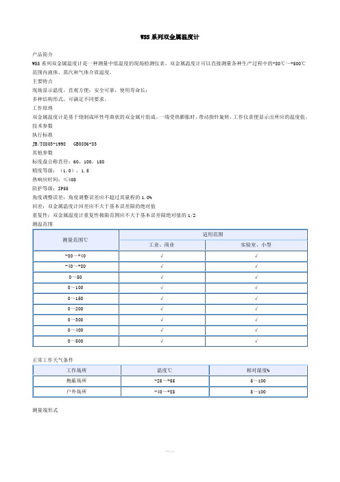
WSS系列双金属温度计产品简介WSS系列双金属温度计是一种测量中低温度的现场检测仪表。
双金属温度计可以直接测量各种生产过程中的-80℃~+500℃范围内液体、蒸汽和气体介质温度。
主要特点现场显示温度,直观方便;安全可靠,使用寿命长;多种结构形式,可满足不同要求。
工作原理双金属温度计是基于绕制成环性弯曲状的双金属片组成。
一端受热膨胀时,带动指针旋转,工作仪表便显示出所应的温度值。
技术参数执行标准JB/T8803-1998 GB3836-83其他参数标度盘公称直径:60,100,150精度等级:(1.0),1.5热响应时间:≤40S防护等级:IP55角度调整误差:角度调整误差应不超过其量程的1.0%回差:双金属温度计回差应不大于基本误差限的绝对值重复性:双金属温度计重复性极限范围应不大于基本误差限绝对值的1/2测温范围正常工作天气条件测量端形式外形及尺寸形式 A B C E L d轴向型65 23 73 -751001502003004005007501000Φ6Φ8Φ10105 23 73 -155 23 73 -径向型65 50 110 34105 50 110 34105 50 110 34135°向型105 23 85 -155 23 85 -万向型105 23 178 120155 23 178 120安装固定形式可动外螺纹管接头M H SW dM16×1.512 18Φ6Φ8Φ10M20×1.516 22M27×220 30NPT1/4 15 18NPT1/2 19 22NPT3/4 25 30可动内螺纹管接头MH SW dM16×1.5 12 18 Φ6 Φ8 Φ10M20×1.5 16 22 M27×2 20 30 NPT1/4 15 18 NPT1/2 19 22 NPT3/42530固定螺纹管接头M H SW dM16×1.5 12 18 Φ6 Φ8 Φ10 M20×1.5 16 22 M27×2 20 30 NPT1/4 15 18 NPT1/2 19 22 NPT3/42530卡套螺纹接头M H SW d M12×1.5 15 19 Φ6 M16×1.5 15 22 Φ8 M20×1.51624Φ10卡套法兰接头D D0 D1 SW d0 d Φ60Φ42Φ24Φ22Φ9Φ8 Φ10固定法兰D D1 D2 H d0 d Φ105Φ75Φ55Φ16Φ14Φ8 Φ10备注:可提供ANSI、JB、HG等标准法兰。
5082-K121-CF000中文资料

Features• Low Power Consumption • Industry Standard Size• Industry Standard Pinout • Choice of Character Size7.6 mm (0.30 in), 10 mm (0.40 in), 10.9 mm (0.43 in), 14.2 mm (0.56 in), 20 mm (0.80 in)• Choice of ColorsAlGaAs Red, High Efficiency Red (HER), Yellow, Green• Excellent Appearance Evenly Lighted Segments±50° Viewing Angle• Design FlexibilityCommon Anode or Common CathodeSingle and Dual DigitLeft and Right Hand Decimal Points±1. Overflow Character• Categorized for Luminous IntensityYellow and Green Categorized for ColorUse of Like Categories Yields a Uniform Display• Excellent for Long Digit String Multiplexing DescriptionThese low current seven segment displays are designed for applica-tions requiring low power consumption. They are tested and selected for their excellent low current characteristics to ensure that the segments are matched at low currents. Drive currents as low as 1 mA per segment are available.Pin for pin equivalent displays are also available in a standard current or high light ambient design. The standard current displays are available in all colors and are ideal for most applica-tions. The high light ambient displays are ideal for sunlight ambients or long string lengths. For additional information see the 7.6 mm Micro Bright Seven Segment Displays, 10 mm Seven Segment Displays, 7.6 mm/10.9 mm Seven Segment Displays, 14.2 mm Seven Segment Displays, 20 mm Seven Segment Displays, or High Light Ambient Seven Segment Displays data sheets.Low Current Seven SegmentDisplays Technical Data HDSP-335x SeriesHDSP-555x SeriesHDSP-751x SeriesHDSP-A10x Series HDSP-A80x Series HDSP-A90x Series HDSP-E10x Series HDSP-F10x Series HDSP-G10x Series HDSP-H10x Series HDSP-K12x, K70x Series HDSP-N10x SeriesHDSP-N40x SeriesDevicesAlGaAs HER Yellow Green Package HDSP-HDSP-HDSP-HDSP-Description Drawing A1017511A801A9017.6 mm Common Anode Right Hand Decimal A A1037513A803A9037.6 mm Common Cathode Right Hand Decimal B A1077517A807A9077.6 mm Common Anode ±1. Overflow C A1087518A808A9087.6 mm Common Cathode ±1. Overflow D F10110 mm Common Anode Right Hand Decimal E F10310 mm Common Cathode Right Hand Decimal F F10710 mm Common Anode ±1. Overflow G F10810 mm Common Cathode ±1. Overflow H G10110 mm Two Digit Common Anode Right Hand Decimal X G10310 mm Two Digit Common Cathode Right Hand Decimal Y E100335010.9 mm Common Anode Left Hand Decimal I E101335110.9 mm Common Anode Right Hand Decimal J E103335310.9 mm Common Cathode Right Hand Decimal K E106335610.9 mm Universal ±1. Overflow[1]L H101555114.2 mm Common Anode Right Hand Decimal M H103555314.2 mm Common Cathode Right Hand Decimal N H107555714.2 mm Common Anode ±1. Overflow O H108555814.2 mm Common Cathode ±1. Overflow P K121K70114.2 mm Two Digit Common Anode Right Hand Decimal R K123K70314.2 mm Two Digit Common Cathode Right Hand Decimal S N10020 mm Common Anode Left Hand Decimal Q N101N40120 mm Common Anode Right Hand Decimal T N103N40320 mm Common Cathode Right Hand Decimal U N10520 mm Common Cathode Left Hand Decimal V N106N40620 mm Universal ±1. Overflow[1]W Note:1. Universal pinout brings the anode and cathode of each segment’s LED out to separate pins. See internal diagrams L or W.Part Numbering System5082-x xx x-x x x xxHDSP-x xx x-x x x xxMechanical Options[1]00: No mechanical optionColor Bin Options[1,2]0: No color bin limitationMaximum Intensity Bin[1,2]0: No maximum intensity bin limitationMinimum Intensity Bin[1,2]0: No minimum intensity bin limitationDevice Configuration/Color[1]G: GreenDevice Specific Configuration[1]Refer to respective datasheetPackage[1]Refer to Respective datasheetNotes:1. For codes not listed in the figure above, please refer to the respective datasheet or contact your nearest Agilent representative fordetails.2. Bin options refer to shippable bins for a part-number. Color and Intensity Bins are typically restricted to 1 bin per tube (excep-tions may apply). Please refer to respective datasheet for specific bin limit information.Package DimensionsPackage Dimensions (cont.)Package Dimensions (cont.)*The Side View of package indicates Country of Origin.Package Dimensions (cont.)Package Dimensions (cont.)Package Dimensions (cont.)Internal Circuit DiagramInternal Circuit Diagram (cont.)Absolute Maximum RatingsAlGaAs Red - HDSP-HERA10X/E10X/H10X HDSP-751X/Yellow GreenK12X/N10X/N40X335X/555X/HDSP-A80X HDSP-A90X Description F10X, G10X Series K70X Series Series Series Units Average Power per Segment or DP375264mW Peak Forward Current per 45mA Segment or DPDC Forward Current per15[1]15[2]mA Segment or DPOperating Temperature Range-20 to +100-40 to +100°C Storage Temperature Range -55 to +100°C Reverse Voltage per Segment 3.0V or DPWave Soldering Temperature for 3Seconds (1.60 mm [0.063 in.] below 250°C seating body)Notes:1. Derate above 91°C at 0.53 mA/°C.2. Derate HER/Yellow above 80°C at 0.38 mA/°C and Green above 71°C at 0.31 mA/°C.Electrical/Optical Characteristics at T A = 25°CAlGaAs RedDeviceSeriesHDSP-Parameter Symbol Min.Typ.Max.Units Test Conditions315600I F = 1 mA A10x3600I F = 5 mA330650I F = 1 mAF10x, G10x3900I F = 5 mA390650I F = 1 mA E10x Luminous Intensity/Segment[1,2]I Vµcd(Digit Average)3900I F = 5 mA400700I F = 1 mAH10x, K12x4200I F = 5 mA270590I F = 1 mAN10x, N40x3500I F = 5 mA1.6I F = 1 mAForward Voltage/Segment or DP V F 1.7V I F = 5 mA1.82.2I F = 20 mA PkAll Devices Peak WavelengthλPEAK645nmDominant Wavelength[3]λd637nmReverse Voltage/Segment or DP[4]V R 3.015V I R = 100 µATemperature Coefficient of∆V F/°C-2 mV mV/°CV F/Segment or DPA10x255F10x, G10x320E10x340Thermal Resistance LED RθJ-PIN°C/W/SegH10x, K12x Junction-to-Pin400N10x, N40x430High Efficiency RedDeviceSeriesHDSP-Parameter Symbol Min.Typ.Max.Units Test Conditions160270I F = 2 mA 751x1050I F = 5 mA200300I F = 2 mA Luminous Intensity/Segment[1,2]I V mcd(Digit Average)1200I F = 5 mA335x, 555x,K70x270370I F = 2 mA1480I F = 5 mA1.6I F = 2 mAForward Voltage/Segment or DP V F 1.7V I F = 5 mA2.1 2.5I F = 20 mA Pk All Devices Peak WavelengthλPEAK635nmDominant Wavelength[3]λd626nmReverse Voltage/Segment or DP[4]V R 3.030V I R = 100 µATemperature Coefficient of∆V F/°C-2mV/°CV F/Segment or DP751x200335x Thermal Resistance LED RθJ-PIN280°C/WJunction-to-Pin555x, K70x345YellowDeviceSeriesHDSP-Parameter Symbol Min.Typ.Max.Units Test Conditions Luminous Intensity/Segment[1,2]250420I F = 4 mA(Digit Average)I V mcd1300I F = 10 mA1.7I F = 4 mAForward Voltage/Segment or DP V F 1.8V I F = 5 mA A80x2.1 2.5I F = 20 mA PkPeak WavelengthλPEAK583nmDominant Wavelength[3,5]λd581.5585592.5nmReverse Voltage/Segment or DP[4]V R 3.030V I R = 100 µATemperature Coefficient of∆V F/°C-2mV/°CV F/Segment or DPThermal Resistance LED RθJ-PIN200°C/WJunction-to-PinGreenDeviceSeriesHDSP-Parameter Symbol Min.Typ.Max.Units Test Conditions Luminous Intensity/Segment[1,2]250475I F = 4 mA(Digit Average)I V mcd1500I F = 10 mA1.9I F = 4 mAForward Voltage/Segment or DP V F 2.0V I F = 10 mA A90x2.1 2.5I F = 20 mA PkPeak WavelengthλPEAK566nmDominant Wavelength[3,5]λd571577nmReverse Voltage/Segment or DP[4]V R 3.030V I R = 100 µATemperature Coefficient of∆V F/°C-2mV/°CV F/Segment or DPThermal Resistance LED RθJ-PIN200°C/WJunction-to-PinNotes:1. Device case temperature is 25°C prior to the intensity measurement.2. The digits are categorized for luminous intensity. The intensity category is designated by a letter on the side of the package.3. The dominant wavelength, λd, is derived from the CIE chromaticity diagram and is the single wavelength which defines the color of thedevice.4. Typical specification for reference only. Do not exceed absolute maximum ratings.5. The yellow (HDSP-A800) and Green (HDSP-A900) displays are categorized for dominant wavelength. The category is designated by anumber adjacent to the luminous intensity category letter.Figure 1. Maximum AllowableAverage or DC Current vs. Ambient Temperature.Figure 2. Forward Current vs.Forward Voltage.AlGaAs RedFigure 4. Relative Efficiency (Luminous Intensity per UnitCurrent) vs. Peak Current.Figure 3. Relative Luminous Intensity vs. DC Forward Current.Figure 5. Maximum Allowable Average or DC Current vs. Ambient Temperature.Figure 6. Forward Current vs. Forward Voltage.HER, Yellow, GreenFigure 7. Relative Luminous Intensityvs. DC Forward Current.Figure 8. Relative Efficiency(Luminous Intensity per UnitCurrent) vs. Peak Current.Intensity Bin Limits (mcd)AlGaAs RedHDSP-A10xIV Bin Category Min.Max.E0.3150.520F0.4280.759G0.621 1.16H0.945 1.71I 1.40 2.56J 2.10 3.84K 3.14 5.75L 4.708.55HDSP-E10x/F10x/G10xIV Bin Category Min.Max.D0.3910.650E0.5320.923F0.755 1.39G 1.13 2.08H 1.70 3.14HDSP-H10x/K12xIV Bin Category Min.Max.C0.4150.690D0.5650.990E0.810 1.50F 1.20 2.20G 1.80 3.30H 2.73 5.00I 4.097.50HDSP-N10xIV Bin Category Min.Max.A0.2700.400B0.3250.500C0.4150.690D0.5650.990E0.810 1.50F 1.20 2.20G 1.80 3.30H 2.73 5.00I 4.097.50Intensity Bin Limits (mcd), continued HERHDSP-751xIV Bin Category Min.Max.B0.1600.240C0.2000.300D0.2500.385E0.3150.520F0.4280.759G0.621 1.16HDSP-751xIV Bin Category Min.Max.B0.2400.366C0.3000.477D0.3910.650E0.5320.923F0.755 1.39G 1.13 2.08H 1.70 3.14HDSP-555x/K70xIV Bin Category Min.Max.A0.2700.400B0.3250.500C0.4150.690D0.5650.990E0.810 1.50F 1.20 2.20G 1.80 3.30H 2.73 5.00I 4.097.50Intensity Bin Limits (mcd), continued YellowHDSP-A80xIV Bin Category Min.Max.D0.2500.385E0.3150.520F0.4250.760G0.625 1.14H0.940 1.70I 1.40 2.56J 2.10 3.84K 3.14 5.76L 4.718.64M7.0713.00N10.6019.40O15.9029.20P23.9043.80Q35.8065.60GreenHDSP-A90xIV Bin Category Min.Max.E0.3150.520F0.4250.760G0.625 1.14H0.940 1.70I 1.40 2.56J 2.10 3.84K 3.14 5.76L 4.718.64M7.0713.00N10.6019.40O15.9029.20P23.9043.80Q35.8065.60Electrical/OpticalFor more information on electrical/optical characteristics, please see Application Note 1005.Contrast Enhancement For information on contrast enhancement, please see Application Note 1015.Soldering/Cleaning Cleaning agents from the ketone family (acetone, methyl ethyl ketone, etc.) and from the chorinated hydrocarbon family (methylene chloride, trichloro-ethylene, carbon tetrachloride, etc.) are not recommended for cleaning LED parts. All of these various solvents attack or dissolve the encapsulating epoxies used to form the package of plastic LED parts.For information on soldering LEDs, please refer to Application Note 1027.Note:All categories are established for classification of products. Productsmay not be available in all categories. Please contact your localAgilent representatives for further clarification/information.Color Categories/semiconductorsFor product information and a complete list ofdistributors, please go to our web site.For technical assistance call:Americas/Canada: +1 (800) 235-0312 or(916) 788 6763Europe: +49 (0) 6441 92460China: 10800 650 0017Hong Kong: (+65) 6271 2451India, Australia, New Zealand: (+65) 6271 2394Japan: (+81 3) 3335-8152(Domestic/International), or0120-61-1280(Domestic Only)Korea: (+65) 6271 2194Malaysia, Singapore: (+65) 6271 2054Taiwan: (+65) 6271 2654Data subject to change.Copyright © 2005 Agilent Technologies, Inc.Obsoletes 5988-8412ENJanuary 19, 20055989-0080EN。
杰弗顿金属分析仪 HS153 说明书
When moisture content determines productivity, the HS153 is the instrument of choice. High speed testing and powerful real-time graphics combined with ruggedness and ease-of-use ensure fast and reproducible measurements in the lab and on the factory floor.
Moisture Analyzer HS153
Boost Productivity In Lab and Factory
Fast and accurate
The 2nd generation halogen technology features precise temperature control for rapid and homogenous heating of the sample, ensuring fast measurements and reproducible results.
Balance Technology Capacity Minimal sample weight Readability Drying unit Technology Temperatur range Lid-opening Routine tests Balance test external weights Balance test internal weights Heating module test
Subject to technical changes © 05/2012 Mettler-Toledo AG Printed in Switzerland 30019626 Global MarCom Switzerland
导热油的应用技术基础知识

导热油应用技术基础知识导热油的概念、用途及发展1、什么是导热油导热油是有机热载体的俗称,我国统一命名为热传导液。
其英文名称为Heat tranferoil,它是以液相或气象形态进行热量传递的介质。
它包括矿物性导热油(称为热传导油)和合成型导热油(称为热传导液)。
2、矿物性导热油和合成型导热油的制取矿物性导热油是石油加工过程中,提取某段馏分,经过精制,再加入多种添加剂制取;合成型导热油是以某种化工或石油化工产品作原料,经过有机合成工艺制取。
合成型导热油是纯的或比较纯的化学品,它与矿物型导热油相比较,具有热稳定性好、使用温度高、寿命长及可再生等特点。
3、导热油的用途、主要用于哪些行业?由于利用导热油与利用蒸汽相比具有加热均匀、操作简单、安全环保、节约能源控温精度高、操作压力低等优点,在现代工业生产中已被作为传热介质得到广泛应用。
广泛应用于石油、化工、油脂、食品、纺织印染、医药、合成纤维、造纸、塑料、橡胶、木材、建材、冶金、机械加工和铸造、空调及电器设备、脂肪和油漆、撂跤、汽车制造、碳素工业中。
还应用于筑路工程中、国防科研中、海运业中。
除上述行业外,还应用于温水发声器、热水发生器、蒸汽发生器、散热器以及肥皂洗涤剂工业、焦油加工业、洗衣业的用热。
4、导热油的发展历史、现状及发展前景导热油的研究和应用始于20世纪30年代前后。
1929年,美国道氏(DOW)化学公司首次生产出联苯醚和联苯的混合物,其商品名称为Dowtherm A,后的专利并应用于加热系统,开创了生产导热油的先河,为热载体的发展开辟了新的途径。
自此,导热油作为一种新的传热介质的优越性逐步为人们所认识。
在欧美市场陆续开发出一些与Dowtherm A组分相似的产品,如德国拜尔公司的Dipnyl 系列产品及Dowtherm E、三氯苯与氯化氢混合物、邻苯二甲酸异丙脂、邻苯二甲酸二乙脂等。
1948年日本也开始了对导热油的研究,1952年生产出sk-OIL260和sk-OIL170的导热油。
- 1、下载文档前请自行甄别文档内容的完整性,平台不提供额外的编辑、内容补充、找答案等附加服务。
- 2、"仅部分预览"的文档,不可在线预览部分如存在完整性等问题,可反馈申请退款(可完整预览的文档不适用该条件!)。
- 3、如文档侵犯您的权益,请联系客服反馈,我们会尽快为您处理(人工客服工作时间:9:00-18:30)。
14.2 mm (0.56 inch)Seven Segment Displays Technical DataFeatures• Industry Standard Size • Industry Standard Pinout 15.24 mm (0.6 in.) DIP Leads on 2.54 mm (0.1 in.) Centers • Choice of ColorsAlGaAs Red, High Efficiency Red, Yellow, Green, Orange • Excellent Appearance Evenly Lighted Segments Mitered Corners on Segments Gray Package Gives Optimum Contrast±50° Viewing Angle • Design FlexibilityCommon Anode or Common CathodeSingle and Dual Digits Right Hand Decimal Point ±1. Overflow Character• Categorized for Luminous IntensityYellow and Green Categorized for ColorUse of Like Categories Yields a Uniform Display • High Light Output • High Peak Current• Excellent for Long Digit String Multiplexing • Intensity and Color Selection OptionSee Intensity and ColorSelected Displays Data Sheet • Sunlight Viewable AlGaAsDescriptionThe 14.2 mm (0.56 inch) LED seven segment displays aredesigned for viewing distances upto 7 metres (23 feet). Thesedevices use an industry standard size package and pinout. Both the numeric and ±1 overflow devices feature a right hand decimalpoint. All devices are available as either common anode or common cathode.Orange AlGaAs Red HERYellowGreen Package HDSP-HDSP-[1]HDSP-[1]HDSP-HDSP- DescriptionDrawingH401H151550157015601Common Anode Right Hand Decimal A H403H153550357035603Common Cathode Right Hand Decimal B H157550757075607Common Anode ±1. Overflow C H158550857085608Common Cathode ±1. OverflowD K401552157215621Two Digit Common Anode Right Hand DecimalE K403552357235623Two Digit Common Cathode Right Hand DecimalFDevicesNote:1. These displays are recommended for high ambient light operation. Please refer to the HDSP-H10X/K12X AlGaAs and HDSP-555X HER data sheet for low current operation.HDSP-K40x Series HDSP-550x Series HDSP-552x Series HDSP-560x Series HDSP-562x Series HDSP-570x Series HDSP-572x Series HDSP-H15x Series HDSP-H40x SeriesThese displays are ideal for most applications. Pin for pin equivalent displays are alsoavailable in a low current design.The low current displays are idealfor portable applications. For additional information see the Low Current Seven Segment Displays data sheet.Part Numbering SystemNotes:1. For codes not listed in the figure above, please refer to the respective datasheet or contact your nearest Agilent representative for details.2. Bin options refer to shippable bins for a part number. Color and Intensity Bins are typically restricted to 1bin per tube (exceptions may apply). Please refer to respective datasheet for specific bin limit information.5082 -X X X X-X X X X X HDSP-X X X X-X X X X XMechanical Options [1]00: No Mechanical Option Color Bin Options [1,2]0: No Color Bin LimitationMaximum Intensity Bin [1,2]0: No Maximum Intensity Bin Limitation Minimum Intensity Bin [1,2]0: No Minimum Intensity Bin Limitation Device Configuration/Color [1]1: Common Anode 3: Common CathodeDevice Specific Configuration [1]Refer to Respective DatasheetPackage [1]H: 14.2 mm (0.56 inch) Single Digit Seven Segment DisplayFUNCTIONPIN AB CDEF1CATHODE e ANODE e CATHODE c ANODE cE CATHODE NO. 1 E ANODE NO. 12CATHODE d ANODE d ANODE c, d CATHODE c, d D CATHODE NO. 1 D ANODE NO. 13ANODE [3]CATHODE [4]CATHODE b ANODE bC CATHODE NO. 1 C ANODE NO. 14CATHODE c ANODE c ANODE a, b, DP CATHODE a, b, DP DP CATHODE NO. 1DP ANODE NO. 15CATHODE DP ANODE DP CATHOPDE DP ANODE DE E CATHODE NO. 1 E ANODE NO. 26CATHODE b ANODE b CATHODE a ANODE aD CATHODE NO. 2 D ANODE NO. 27CATHODE a ANODE a ANODE a, b, DP CATHODE a, b, DP G CATHODE NO. 2G ANODE NO. 28ANODE [3]CATHODE [4]ANODE c, d CATHODE c, d C CATHODE NO. 2 C ANODE NO. 29CATHODE f ANODE f CATHODE d ANODE d DP CATHODE NO. 2DP ANODE NO. 210CATHODE g ANODE g NO PINNO PINB CATHODE NO. 2 B ANODE NO. 211 A CATHODE NO. 2 A ANODE NO. 212 F CATHODE NO. 2 F ANODE NO. 213DIGIT NO. 2 ANODE DIGIT NO. 2 CATHODE 14DIGIT NO. 1 ANODE DIGIT NO. 1 CATHODE 15 B CATHODE NO. 1 B ANODE NO. 116 A CATHODE NO. 1 A ANODE NO. 117G CATHODE NO. 1G ANODE NO. 118F CATHODE NO. 1 F ANODE NO. 1NOTES:1. ALL DIMENSIONS IN MILLIMETRES (INCHES).2. ALL UNTOLERANCED DIMENSIONS ARE FOR REFERENCE ONLY.3. REDUNDANT ANODES.4. REDUNDANT CATHODES.5. FOR HDSP-5600/-5700 SERIES PRODUCT ONLY.Package DimensionsInternal Circuit DiagramNotes:1. See Figure 2 to establish pulsed conditions.2. Derate above 46°C at 0.54 mA/°C.3. See Figure 7 to establish pulsed conditions.4. Derate above 53°C at 0.45 mA/°C.5. See Figure 8 to establish pulsed conditions.HER/Orange HDSP-5500AlGaAs Red HDSP-H40x Yellow Green HDSP-H150HDSP-K40x HDSP-5700HDSP-5600 Description SeriesSeriesSeriesSeriesUnits Average Power per Segment or DP 9610580105mW Peak Forward Current per 160[1]90[3]60[5]90[7]mA Segment or DPDC Forward Current per Segment or DP 40[2]30[4]20[6]3018]mA Operating Temperature Range -20 to +100[9]-40 to +100°C Storage Temperature Range -55 to +100°C Reverse Voltage per Segment or DP 3.0V Lead Solder Temperature for 3 Seconds 260°C(1.60 mm [0.063 in.] below seating plane)Absolute Maximum Ratings6. Derate above 81°C at 0.52 mA/°C.7. See Figure 9 to establish pulsed conditions.8. Derate above 39°C at 0.37 mA/°C.9. For operation below -20°C, contact your local Agilent components sales office or an authorized distributor.Electrical/Optical Characteristics at T A = 25°CAlGaAs RedDeviceSeriesHDSP- Parameter Symbol Min.Typ.Max.Units Test Conditions Luminous Intensity/Segment[1,2,5]I V9.116.0mcd I F = 20 mA(Digit Average)1.8I F = 20 mAForward Voltage/Segment or DP V F V2.03.0I F = 100 mAH15XPeak WavelengthλPEAK645nmDominant Wavelength[3]λd637nmReverse Voltage/Segment or DP[4]V R 3.015V I R = 100 µATemperature Coefficient of∆V F/°C-2mV/°CV F/Segment or DPThermal Resistance LED Junction-RθJ-Pin400°C/W/to-Pin SegHigh Efficiency RedDeviceSeriesHDSP- Parameter Symbol Min.Typ.Max.Units Test Conditions9002800I F = 10 mA Luminous Intensity/Segment[1,2,6]I Vµcd(Digit Average)3700I F = 60 mA Peak:1 of 6 dfForward Voltage/Segment or DP V F 2.1 2.5V I F = 20 mA 55XXPeak WavelengthλPEAK635nmDominant Wavelength[3]λd626nmReverse Voltage/Segment or DP[4]V R 3.030V I R = 100 µATemperature Coefficient of∆V F/°C-2mV/°CV F/Segment or DPThermal Resistance LED Junction-RθJ-Pin345°C/W/to-Pin SegYellowDeviceSeriesHDSP- Parameter Symbol Min.Typ.Max.Units Test Conditions6001800I F = 10 mA Luminous Intensity/Segment[1,2]I Vµcd(Digit Average)2750I F = 60 mA Peak:1 of 6 dfForward Voltage/Segment or DP V F 2.1 2.5V I F = 20 mA 57XXPeak WavelengthλPEAK583nmDominant Wavelength[3,7]λd581.5586592.5nmReverse Voltage/Segment or DP[4]V R 3.040V I R = 100 µATemperature Coefficient of∆V F/°C-2mV/°CV F/Segment or DPThermal Resistance LED Junction-RθJ-Pin345°C/W/to-Pin SegOrangeDeviceSeriesHDSP- Parameter Symbol Min.Typ.Max.Units Test Conditions Luminous Intensity/Segment I V 2.37mcd I F = 10 mA(Segment Average)[1,2]Forward Voltage/Segment or DP V F 2.1 2.5V I F = 20 mAPeak WavelengthλPEAK600nm H40x Dominant Wavelength[3]λd603nm I F = 10 mA K40x Reverse Voltage/Segment or DP[4]V R 3.030V I R = 100 µA Temperature Coefficient of∆V F/°C-2mV/°CV F/Segment or DPThermal Resistance LED Junction-RθJ-Pin345°C/W/to-Pin SegDeviceSeries HDSP-ParameterSymbol Min.Typ.Max.UnitsTest Conditions 9002500I F = 10 mALuminous Intensity/Segment [1,2]I Vµcd(Digit Average)`3100I F = 60 mA Peak:1 of 6 df Forward Voltage/Segment or DPV F 2.1 2.5V I F = 10 mA56XXPeak Wavelength λPEAK 566nm Dominant Wavelength [3,7]λd 571577nm Reverse Voltage/Segment or DP [4]V R 3.050V I R = 100 µATemperature Coefficient of ∆V F /°C -2mV/°C V F /Segment or DPThermal Resistance LED Junction-R θJ-Pin345°C/W/to-PinSegHigh Performance GreenNotes:1. Device case temperature is 25°C prior to the intensity measurement.2. The digits are categorized for luminous intensity. The intensity category is designated by a letter on the side of the package.3. The dominant wavelength, λd , is derived from the CIE chromaticity diagram and is that single wavelength which defines the color of the device.4. Typical specification for reference only. Do not exceed absolute maximum ratings.5. For low current operation, the AlGaAs HDSP-H10X series displays are recommended. They are tested at 1 mA dc/segment and are pin for pin compatible with the HDSP-H15X series.6. For low current operation, the HER HDSP-555X series displays are recommended. They are tested at 2 mA dc/segment and are pin for pin compatible with the HDSP-550X series.7. The Yellow (HDSP-5700) and Green (HDSP-5600) displays are categorized for dominant wavelength. The category is designated by a number adjacent to the luminous intensity category letter.AlGaAs RedFigure 2. Maximum Tolerable Peak Current vs. Pulse Duration – AlGaAs Red.Figure 1. Maximum Tolerable Peak Current vs.Pulse Duration – Red.Figure 3. Maximum Allowable DC Current vs.Ambient Temperature.Figure 4. Forward Current vs.Forward Voltage.HER, Yellow, Green, OrangeFigure 7. Maximum Tolerable Peak Currentvs. Pulse Duration – HER, Orange.Figure 8. Maximum Tolerable Peak Current vs. Pulse Duration – Yellow.Figure 5. Relative Luminous Intensity vs. DC Forward Current.Figure 6. Relative Efficiency (Luminous Intensity per Unit Current) vs. Peak Current.I D C M A X . – M A X I M U M D C C U R R E N T P E R S E G M E N T – m AT A – AMBIENT TEMPERATURE – °C 5030102051525354045I F – F O R W A R D C U R R E N T P E R S E G M E N T – m AV F – FORWARD VOLTAGE – VR E L A T I V E L U M I N O U S I N T E N S I T Y (N O R M A L I Z E D T O 1 A T 20 m A )I F – FORWARD CURRENT PER SEGMENT – mA204010305152535ηP E A K – N O R M A L IZ E D R E L A T I V E E F F I C I E N C YI PEAK – PEAK FORWARD CURRENTPER SEGMENT – mA40051015202530352010090807060504030T – AMBIENT TEMPERATURE – °C AI M A X – M A X I M U M D C C U R R E N T P E R S E G M E N T – m AD C 4550110120Figure 11. Forward Current vs.Forward Voltage.Figure 9. Maximum Tolerable PeakCurrent vs. Pulse Duration – Green.Figure 10. Maximum Allowable DC Current vs.Ambient Temperature.Figure 12. Relative LuminousIntensity vs. DC Forward Current.Figure 13. Relative Efficiency (Luminous Intensity per Unit Current) vs. Peak Current.Electrical/OpticalFor more information onelectrical/optical characteristics,please see Application Note 1005.Contrast EnhancementFor information on contrastenhancement please see Application Note 1015.Soldering/CleaningCleaning agents from the ketone family (acetone, methyl ethyl ketone, etc.) and from thechlorinated hydrocarbon family(methylene chloride, trichloro–ethylene, carbon tetrachloride,etc.) are not recommended for cleaning LED parts. All of these various solvents attack or dissolve the encapsulating epoxies used to form the package of plastic LED parts.For information on soldering LEDs please refer to Application Note 1027.I F – F O R W A R D C U R R E N T P E R S E G M E N T – m AV F – FORWARD VOLTAGE – VR E L A T I V E L U M I N O U S I N T E N S I T Y (N O R M A L I Z E D A T 10 m A )I F – DC FORWARD CURRENT – mAηV – R E L A T I V E E F F I C I E N C Y (N O R M A L I Z E D T O 1 A T 10 m A P E R S E G M EN T )0.6I PEAK – PEAK FORWARD CURRENTPER SEGMENT – mA902070801001.61.41.31.10.90.860504030100.71.01.21.5HDSP-H15x IV Bin Category Min.Max.K 9.2016.90L 13.8025.30M 20.7038.00N 31.1056.90O 46.6085.40Intensity Bin Limits (mcd)AlGaAs RedHDSP-550x/552x IV Bin Category Min.Max.E 0.91 1.67F 1.37 2.51G 2.05 3.76H 3.08 5.64I 4.628.64J 6.9312.70K 10.3919.04HERHDSP-570x/572xIV Bin Category Min.Max.D 0.61 1.11E 0.91 1.67F 1.37 2.51G 2.05 3.76H 3.08 5.64I 4.628.64J 6.9312.70K 10.3919.04YellowHDSP-560x/562x IV Bin Category Min.Max.E 0.91 1.67F 1.37 2.51G 2.05 3.76H 3.08 5.64I 4.618.46GreenColor CategoriesNote:All categories are established for classification of products. Products may not be available in all categories. Please contact your Agilent representatives for further clarification/information.10HDSP-H40x/K40x IV Bin Category Min.Max.B 0.77 1.17C 0.95 1.45D 1.19 1.82E 1.49 2.27F 1.85 2.89G 2.32 3.54H 2.904.43Orange元器件交易网元器件交易网/semiconductorsFor product information and a complete list ofdistributors, please go to our web site.For technical assistance call:Americas/Canada: +1 (800) 235-0312 or(408) 654-8675Europe: +49 (0) 6441 92460China: 10800 650 0017Hong Kong: (+65) 271 2451India, Australia, New Zealand: (+65) 271 2394Japan: (+81 3) 3335-8152(Domestic/Interna-tional), or 0120-61-1280(Domestic Only)Korea: (+65) 271 2194Malaysia, Singapore: (+65) 271 2054Taiwan: (+65) 271 2654Data subject to change.Copyright © 2002 Agilent Technologies, Inc.Obsoletes 5988-0383ENJanuary 17, 20025988-4273EN。