BT151S-650R贴片单向可控硅晶闸管
MTC300A1600V可控硅晶闸管模块
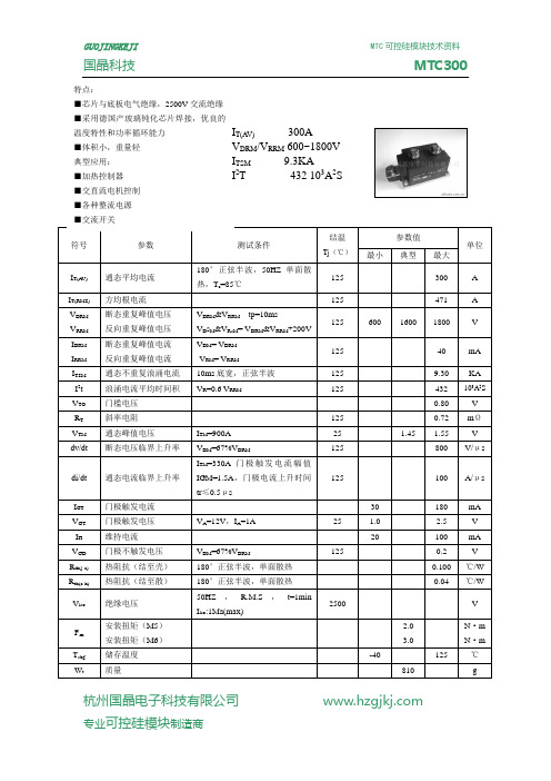
杭州国晶电子科技有限公司杭州国晶电子科技有限公司杭州国晶电子科技有限公司 模块典型电路 电联结形式(右图)散热形式:风冷型模块外型图M353 散热形式:水冷型模块外型图M353S使用说明:一、使用条件及注意事项:1、使用环境应无剧烈振动和冲击,环境介质中应无腐蚀金属和破坏绝缘的杂质和气氛。
2、模块管芯工作结温:可控硅为-40℃∽125℃;环境温度不得高于40℃;环境湿度小于86%。
3、模块在使用前一定要加装散热器,散热器的选配见下节。
散热可采用自然冷却、强迫风冷或水冷。
强迫风冷时,风速应大于6米∕秒。
二、安装注意事项:1、由于MTC可控硅模块是绝缘型(即模块接线柱对铜底板之间的绝缘耐压大于2.5KV有效值),因此可以把多个模块安装在同一散热器上,或装置的接地外壳上。
2、散热器安装表面应平整、光滑,不能有划痕、磕碰和杂物。
散热器表面光洁度应小于10μm。
模块安装到散热器上时,在它们的接触面之间应涂一层很薄的导热硅脂。
涂脂前,用细砂纸把散热器接触面的氧化层去掉,然后用无水乙醇把表面擦干净,使接触良好,以减少热阻。
模块紧固到散热器表面时,采用M5或M6螺钉和弹簧垫圈,并以4NM力矩紧固螺钉杭州国晶电子科技有限公司与模块主电极的连线应采用铜排,并有光滑平整的接触面,使接触良好。
模块工作3小时后,各个螺钉须再次紧固一遍。
模块散热器选择用户选配散热器时,必须考虑以下因素:①模块工作电流大小,以决定所需散热面积;②使用环境,据此可以确定采取什么冷却方式——自然冷却、强迫风冷、还是水冷;③装置的外形、体积、给散热器预留空间的大小,据此可以确定采用什么形状的散热器。
一般而论,大多数用户会选择铝型材散热器。
为方便用户,对我公司生产的各类模块,在特性参数表中都给出了所需散热面积。
此面积是在模块满负荷工作且在强迫风冷时的参考值。
下面给出散热器长度的计算公式:模块所需散热面积=(散热器周长)×(散热器长度)+(截面积)×2其中,模块所需散热面积为模块特性参数表中给出的参考值,散热器周长、截面积可以在散热器厂家样本中查到,散热器长度为待求量。
可控硅的符号
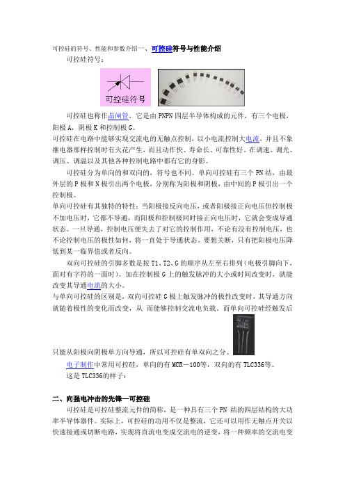
可控硅的符号、性能和参数介绍一、可控硅符号与性能介绍可控硅符号:可控硅也称作晶闸管,它是由PNPN四层半导体构成的元件,有三个电极,阳极A,阴极K和控制极G。
可控硅在电路中能够实现交流电的无触点控制,以小电流控制大电流,并且不象继电器那样控制时有火花产生,而且动作快、寿命长、可靠性好。
在调速、调光、调压、调温以及其他各种控制电路中都有它的身影。
可控硅分为单向的和双向的,符号也不同。
单向可控硅有三个PN结,由最外层的P极和N极引出两个电极,分别称为阳极和阴极,由中间的P极引出一个控制极。
单向可控硅有其独特的特性:当阳极接反向电压,或者阳极接正向电压但控制极不加电压时,它都不导通,而阳极和控制极同时接正向电压时,它就会变成导通状态。
一旦导通,控制电压便失去了对它的控制作用,不论有没有控制电压,也不论控制电压的极性如何,将一直处于导通状态。
要想关断,只有把阳极电压降低到某一临界值或者反向。
双向可控硅的引脚多数是按T1、T2、G的顺序从左至右排列(电极引脚向下,面对有字符的一面时)。
加在控制极G上的触发脉冲的大小或时间改变时,就能改变其导通电流的大小。
与单向可控硅的区别是,双向可控硅G极上触发脉冲的极性改变时,其导通方向就随着极性的变化而改变,从而能够控制交流电负载。
而单向可控硅经触发后只能从阳极向阴极单方向导通,所以可控硅有单双向之分。
电子制作中常用可控硅,单向的有MCR-100等,双向的有TLC336等。
这是TLC336的样子:二、向强电冲击的先锋—可控硅可控硅是可控硅整流元件的简称,是一种具有三个PN 结的四层结构的大功率半导体器件。
实际上,可控硅的功用不仅是整流,它还可以用作无触点开关以快速接通或切断电路,实现将直流电变成交流电的逆变,将一种频率的交流电变成另一种频率的交流电,等等。
可控硅和其它半导体器件一样,其有体积小、效率高、稳定性好、工作可靠等优点。
它的出现,使半导体技术从弱电领域进入了强电领域,成为工业、农业、交通运输、军事科研以至商业、民用电器等方面争相采用的元件。
单向可控硅和双向可控硅原理及应用大全
可控硅元件的工作原理及基本特性1、工作原理可控硅是P1N1P2N2四层三端结构元件,共有三个PN结,分析原理时,可以把它看作由一个PNP管和一个NPN管所组成,其等效图解如图1所示图1 可控硅等效图解图当阳极A加上正向电压时,BG1和BG2管均处于放大状态。
此时,如果从控制极G 输入一个正向触发信号,BG2便有基流ib2流过,经BG2放大,其集电极电流ic2=β2ib2。
因为BG2的集电极直接与BG1的基极相连,所以ib1=ic2。
此时,电流ic2再经BG1放大,于是BG1的集电极电流ic1=β1ib1=β1β2ib2。
这个电流又流回到BG2的基极,表成正反馈,使ib2不断增大,如此正向馈循环的结果,两个管子的电流剧增,可控硅使饱和导通。
由于BG1和BG2所构成的正反馈作用,所以一旦可控硅导通后,即使控制极G的电流消失了,可控硅仍然能够维持导通状态,由于触发信号只起触发作用,没有关断功能,所以这种可控硅是不可关断的。
由于可控硅只有导通和关断两种工作状态,所以它具有开关特性,这种特性需要一定的条件才能转化,此条件见表1表1 可控硅导通和关断条件状态条件说明从关断到导通1、阳极电位高于是阴极电位2、控制极有足够的正向电压和电流两者缺一不可维持导通1、阳极电位高于阴极电位2、阳极电流大于维持电流两者缺一不可从导通到关断1、阳极电位低于阴极电位2、阳极电流小于维持电流任一条件即可2、基本伏安特性可控硅的基本伏安特性见图2图2 可控硅基本伏安特性(1)反向特性当控制极开路,阳极加上反向电压时(见图3),J2结正偏,但J1、J2结反偏。
此时只能流过很小的反向饱和电流,当电压进一步提高到J1结的雪崩击穿电压后,接差J3结也击穿,电流迅速增加,图3的特性开始弯曲,如特性OR段所示,弯曲处的电压URO叫“反向转折电压”。
此时,可控硅会发生永久性反向击穿。
图3 阳极加反向电压(2)正向特性当控制极开路,阳极上加上正向电压时(见图4),J1、J3结正偏,但J2结反偏,这与普通PN结的反向特性相似,也只能流过很小电流,这叫正向阻断状态,当电压增加,图3的特性发生了弯曲,如特性OA段所示,弯曲处的是UBO叫:正向转折电压图4 阳极加正向电压由于电压升高到J2结的雪崩击穿电压后,J2结发生雪崩倍增效应,在结区产生大量的电子和空穴,电子时入N1区,空穴时入P2区。
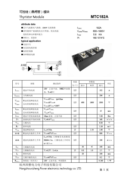
晶闸管模块MTC182A
B
绝缘电压
F mB
B
T sbg B
B
W tB B
Outline
安装扭矩(M5) 安装扭矩(M6) 储存温度 质量(约)
180°正弦半波,单面散热
50HZ , R.M.S , t=1min
IBiso
:1mA
B
(ma
x)
与散热器固定
M234
MTC182A
0.08 ℃/W
2500
V
4.0±15%
5.0±15%
-40
125
205
N·m N·m
℃
g
杭州西整电力电子科技有限公司
Hangzhouxizheng Power electronics technology co. LTD.
第2页
可控硅(晶闸管)模块 Thyristor Module
MTC182A
杭州西整电力电子科技有限公司
Hangzhouxizheng Power electronics technology co. LTD.
可控硅(晶闸管)模块 Thyristor Module
MTC182A
matters needing attention: 1、模块实际负载电流大于 5A 时务必要加装散热器,需提供良好的通风条件。 2、工作环境温度高于 40℃时,应优化散热通风条件。 3、模块工作后会发热,在设备未断电及模块未完全冷却降温之前,严禁用手触摸模块
B
DRM B
B
RBth(j-c)B
热阻抗(结至壳)
180°正弦半波,单面散热
杭州西整电力电子科技有限公司
30
25
0.8
20
125
Hangzhouxizheng Power electronics technology co. LTD.
107na0可控硅参数

107na0可控硅参数1. 可控硅的基本概念和原理可控硅(SCR)是一种半导体器件,也被称为双向可控硅。
它是一种具有控制电流流动的能力的二极管。
可控硅的主要特点是具有一定的触发电压,当触发电压施加到可控硅的控制端时,可控硅会进入导通状态,电流开始流动;当触发电压被去除时,可控硅会进入截止状态,电流停止流动。
可控硅的原理是基于PN结的特性,它由四层半导体材料构成,其中有三个PN结。
当可控硅未触发时,PN结处于正向偏置状态,电流无法通过;当触发电压施加到控制端时,PN结会反向击穿,形成一个导通路径,电流开始流动。
2. 可控硅的主要参数2.1 触发电压(Vgt)触发电压是指施加到可控硅控制端的电压,当电压达到一定阈值时,可控硅会进入导通状态。
触发电压是可控硅的一个重要参数,不同型号的可控硅具有不同的触发电压。
2.2 阻断电压(Vdrm)阻断电压是指可控硅在截止状态下能够承受的最大电压。
当施加到可控硅的电压超过阻断电压时,可控硅会被击穿,导致电流流动,这是不可控的。
因此,选择合适的阻断电压对于可控硅的应用非常重要。
2.3 保持电流(Ih)保持电流是指可控硅在导通状态下需要维持的最小电流。
如果电流低于保持电流,可控硅会自动进入截止状态。
保持电流的大小取决于可控硅的结构和性能。
2.4 导通电压降(Vtm)导通电压降是指可控硅在导通状态下的电压降。
导通电压降是可控硅的一个重要参数,它影响可控硅的功耗和效率。
较低的导通电压降可以减少能量损耗,提高可控硅的效率。
3. 可控硅的应用3.1 交流电控制可控硅可以用于交流电控制,例如调光、电压调节和电流控制等。
通过控制可控硅的触发电压和导通角,可以实现对交流电的精确控制。
3.2 直流电控制可控硅也可以用于直流电控制,例如电机控制和直流电源调节等。
通过控制可控硅的触发电压和导通角,可以实现对直流电的精确控制。
3.3 开关控制可控硅可以作为开关使用,用于电路的开关控制。
通过控制可控硅的触发电压,可以实现对电路的开关操作,从而实现对电路的控制。
BT151-650R中文资料
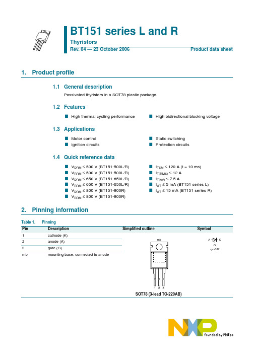
1.Product profile1.1General descriptionPassivated thyristors in a SOT78 plastic package.1.2Features1.3Applications1.4Quick reference data2.Pinning informationBT151 series L and RThyristorsRev. 04 — 23 October 2006Product data sheetI High thermal cycling performanceI High bidirectional blocking voltageI Motor control I Static switching I Ignition circuitsI Protection circuitsI V DRM ≤500V (BT151-500L/R)I I TSM ≤120A (t =10ms)I V RRM ≤500V (BT151-500L/R)I I T(RMS)≤12A I V DRM ≤650V (BT151-650L/R)I I T(AV)≤7.5AI V RRM ≤650V (BT151-650L/R)I I GT ≤5mA (BT151 series L)I V DRM ≤800V (BT151-800R)II GT ≤15mA (BT151 series R)IV RRM ≤800V (BT151-800R)Table 1.PinningPin Description Simplified outline Symbol1cathode (K)SOT78 (3-lead TO-220AB)2anode (A)3gate (G)mbmounting base; connected to anode12mb3sym037AKG3.Ordering information4.Limiting values[1]Although not recommended,off-state voltages up to 800V may be applied without damage,but the thyristor may switch to the on-state.The rate of rise of current should not exceed 15A/µs.Table 2.Ordering informationType numberPackage NameDescriptionVersion BT151-500L SC-46plastic single-ended package; heatsink mounted; 1 mounting hole;3-lead TO-220ABSOT78BT151-500R BT151-650L BT151-650R BT151-800RTable 3.Limiting valuesIn accordance with the Absolute Maximum Rating System (IEC 60134).Symbol ParameterConditionsMin Max Unit V DRMrepetitive peak off-state voltageBT151-500L; BT151-500R [1]-500V BT151-650L; BT151-650R [1]-650V BT151-800R-800V V RRMrepetitive peak reverse voltageBT151-500L; BT151-500R [1]-500V BT151-650L; BT151-650R [1]-650V BT151-800R-800V I T(AV)average on-state current half sine wave; T mb ≤109°C;see Figure 1-7.5A I T(RMS)RMS on-state current all conduction angles;see Figure 4and 5-12AI TSMnon-repetitive peak on-state currenthalf sine wave; T j =25°C prior to surge; see Figure 2and 3t =10ms -120A t =8.3ms-132A I 2t I 2t for fusingt =10ms-72A 2s dI T /dt rate of rise of on-state current I TM =20A; I G =50mA;dI G /dt =50 mA/µs-50A/µs I GM peak gate current -2A V RGM peak reverse gate voltage -5V P GM peak gate power -5W P G(AV)average gate power over any 20ms period -0.5W T stg storage temperature −40+150°C T jjunction temperature-125°CForm factor a =I T(RMS)/I T(AV)Fig 1.Total power dissipation as a function of average on-state current; maximum valuesf =50HzFig 2.Non-repetitive peak on-state current as a function of the number of sinusoidal current cycles; maximumvaluesI T(AV) (A)8642001aaa95851015P tot (W)0118.5112105.5T mb(max)(°C)125a =1.5742.82.21.9conduction angle (degrees)form factor a 30609012018042.82.21.91.57α001aaa9578040120160 I TSM (A)0n110310210t pT j initial = 25 °C max I TI TSMtt p ≤10msFig 3.Non-repetitive peak on-state current as a function of pulse width for sinusoidal currents;maximum valuesf =50Hz; T mb ≤109°CFig 4.RMS on-state current as a function of surgeduration; maximum values Fig 5.RMS on-state current as a function of mountingbase temperature; maximum values001aaa956t p (s)10−510−210−310−4102103I TSM (A)10dl T /dt limitt pT j initial = 25 °C maxI TI TSMt surge duration (s)10−210110−1001aaa954101552025I T(RMS)(A)0T mb (°C)−50150100050001aaa999841216I T(RMS)(A)5.Thermal characteristicsTable 4.Thermal characteristics Symbol ParameterConditions Min Typ Max Unit R th(j-mb)thermal resistance from junction to mounting basesee Figure 6-- 1.3K/W R th(j-a)thermal resistance from junction to ambientin free air-60-K/WFig 6.Transient thermal impedance from junction to mounting base as a function of pulse width001aaa96210−110−2110Z th(j-mb)(K/W)10−3t p (s)10−511010−110−210−410−3t pt p TPtTδ =6.CharacteristicsTable 5.CharacteristicsT j = 25°C unless otherwise stated.Symbol Parameter Conditions Min Typ Max Unit Static characteristicsI GT gate trigger current V D=12V; I T=100mA; see Figure8BT151-500L-25mABT151-500R-215mABT151-650L-25mABT151-650R-215mABT151-800R-215mA I L latching current V D=12V; I GT=100mA; seeFigure10-1040mAI H holding current V D=12V; I GT=100mA; seeFigure11-720mA V T on-state voltage I T=23A; see Figure9- 1.4 1.75VV GT gate trigger voltage I T=100mA; V D=12V; see Figure7-0.6 1.5VI T=100mA; V D=V DRM(max);T j=125°C0.250.4-VI D off-state current V D=V DRM(max); T j=125°C-0.10.5mA I R reverse current V R=V RRM(max); T j=125°C-0.10.5mA Dynamic characteristicsdV D/dt rate of rise of off-statevoltage V DM=0.67× V DRM(max); T j=125°C;exponential waveform; see Figure12R GK=100Ω2001000-V/µs gate open circuit50130-V/µst gt gate-controlled turn-ontime I TM=40A; V D=V DRM(max);I G=100mA; dI G/dt=5A/µs-2-µst q commutated turn-offtime V DM=0.67× V DRM(max); T j=125°C;I TM=20A; V R=25V;(dI T/dt)M=30A/µs; dV D/dt=50V/µs;R GK=100Ω-70-µsFig 7.Normalized gate trigger voltage as a function ofjunction temperatureFig 8.Normalized gate trigger current as a function ofjunction temperatureV o =1.06V R s =0.0304Ω(1)T j =125°C; typical values (2)T j =125°C; maximum values (3)T j =25°C; maximum valuesFig 9.On-state current as a function of on-statevoltage Fig 10.Normalized latching current as a function ofjunction temperatureT j (°C)−50150100050001aaa9530.81.21.60.4V GT V GT(25°C)T j (°C)−50150100050001aaa9521230I GT I GT(25°C)V T (V)021.50.51001aaa959102030I T (A)0(3)(2)(1)T j (°C)−50150100050001aaa9511230I L I L(25°C)(1) R GK =100Ω(2) Gate open circuitFig 11.Normalized holding current as a function ofjunction temperatureFig 12.Critical rate of rise of off-state voltage as afunction of junction temperature; minimum valuesT j (°C)−50150100050001aaa950123I H I H(25°C)0001aaa949103102104dV D /dt (V/µs)10T j (°C)015010050(2)(1)7.Package outlineFig 13.Package outline SOT78 (TO-220AB)REFERENCESOUTLINE VERSION EUROPEAN PROJECTIONISSUE DATE IECJEDEC JEITA SOT78SC-463-lead TO-220ABDD 1qpL123L 1b 1e eb0510 mmscalePlastic single-ended package; heatsink mounted; 1 mounting hole; 3-lead TO-220ABSOT78DIMENSIONS (mm are the original dimensions)A E A 1cQL 2UNIT A 1b 1D 1e p mm2.54q Q A b D c L 2max.3.03.83.515.012.83.302.793.02.72.62.20.70.416.015.20.90.61.451.004.74.11.401.256.65.910.39.7L 1E L 05-03-2205-10-25mounting base8.Revision historyTable 6.Revision historyDocument ID Release date Data sheet status Change notice SupersedesBT151_SER_L_R_420061023Product data sheet-BT151_SERIES_3 Modifications:•The format of this data sheet has been redesigned to comply with the new identityguidelines of NXP Semiconductors.•Legal texts have been adapted to the new company name where appropriate.•Added type numbers BT151-500L and BT151-650LBT151_SERIES_320040607Product specification-BT151_SERIES_2 (939775013159)BT151_SERIES_219990601Product specification-BT151_SERIES_1 BT151_SERIES_119970901Product specification--BT151_SER_L_R_4© NXP B.V . 2006. All rights reserved.Product data sheet Rev. 04 — 23 October 200611 of 129.Legal information9.1Data sheet status[1]Please consult the most recently issued document before initiating or completing a design.[2]The term ‘short data sheet’ is explained in section “Definitions”.[3]The product status of device(s)described in this document may have changed since this document was published and may differ in case of multiple devices.The latest product status information is available on the Internet at URL .9.2DefinitionsDraft —The document is a draft version only. The content is still under internal review and subject to formal approval, which may result in modifications or additions. NXP Semiconductors does not give any representations or warranties as to the accuracy or completeness ofinformation included herein and shall have no liability for the consequences of use of such information.Short data sheet —A short data sheet is an extract from a full data sheet with the same product type number(s)and title.A short data sheet is intended for quick reference only and should not be relied upon to contain detailed and full information. For detailed and full information see the relevant full data sheet, which is available on request via the local NXP Semiconductors sales office. In case of any inconsistency or conflict with the short data sheet, the full data sheet shall prevail.9.3DisclaimersGeneral —Information in this document is believed to be accurate andreliable.However,NXP Semiconductors does not give any representations or warranties,expressed or implied,as to the accuracy or completeness of such information and shall have no liability for the consequences of use of such information.Right to make changes —NXP Semiconductors reserves the right to make changes to information published in this document, including withoutlimitation specifications and product descriptions, at any time and without notice.This document supersedes and replaces all information supplied prior to the publication hereof.Suitability for use —NXP Semiconductors products are not designed,authorized or warranted to be suitable for use in medical, military, aircraft,space or life support equipment, nor in applications where failure ormalfunction of a NXP Semiconductors product can reasonably be expected to result in personal injury, death or severe property or environmental damage.NXP Semiconductors accepts no liability for inclusion and/or use of NXP Semiconductors products in such equipment or applications and therefore such inclusion and/or use is at the customer’s own risk.Applications —Applications that are described herein for any of these products are for illustrative purposes only. NXP Semiconductors makes no representation or warranty that such applications will be suitable for the specified use without further testing or modification.Limiting values —Stress above one or more limiting values (as defined in the Absolute Maximum Ratings System of IEC 60134)may cause permanent damage to the device.Limiting values are stress ratings only and operation of the device at these or any other conditions above those given in theCharacteristics sections of this document is not implied. Exposure to limiting values for extended periods may affect device reliability.Terms and conditions of sale —NXP Semiconductors products are sold subject to the general terms and conditions of commercial sale,as published at /profile/terms , including those pertaining to warranty,intellectual property rights infringement and limitation of liability, unless explicitly otherwise agreed to in writing by NXP Semiconductors. In case of any inconsistency or conflict between information in this document and such terms and conditions, the latter will prevail.No offer to sell or license —Nothing in this document may be interpreted or construed as an offer to sell products that is open for acceptance or the grant,conveyance or implication of any license under any copyrights,patents or other industrial or intellectual property rights.9.4TrademarksNotice:All referenced brands,product names,service names and trademarks are the property of their respective owners.10.Contact informationFor additional information, please visit:For sales office addresses, send an email to:salesaddresses@Document status [1][2]Product status [3]DefinitionObjective [short] data sheet Development This document contains data from the objective specification for product development.Preliminary [short] data sheet Qualification This document contains data from the preliminary specification.Product [short] data sheetProductionThis document contains the product specification.11.Contents1Product profile. . . . . . . . . . . . . . . . . . . . . . . . . . 11.1General description. . . . . . . . . . . . . . . . . . . . . . 11.2Features . . . . . . . . . . . . . . . . . . . . . . . . . . . . . . 11.3Applications . . . . . . . . . . . . . . . . . . . . . . . . . . . 11.4Quick reference data. . . . . . . . . . . . . . . . . . . . . 12Pinning information. . . . . . . . . . . . . . . . . . . . . . 13Ordering information. . . . . . . . . . . . . . . . . . . . . 24Limiting values. . . . . . . . . . . . . . . . . . . . . . . . . . 25Thermal characteristics. . . . . . . . . . . . . . . . . . . 56Characteristics. . . . . . . . . . . . . . . . . . . . . . . . . . 67Package outline . . . . . . . . . . . . . . . . . . . . . . . . . 98Revision history. . . . . . . . . . . . . . . . . . . . . . . . 109Legal information. . . . . . . . . . . . . . . . . . . . . . . 119.1Data sheet status . . . . . . . . . . . . . . . . . . . . . . 119.2Definitions. . . . . . . . . . . . . . . . . . . . . . . . . . . . 119.3Disclaimers. . . . . . . . . . . . . . . . . . . . . . . . . . . 119.4T rademarks. . . . . . . . . . . . . . . . . . . . . . . . . . . 1110Contact information. . . . . . . . . . . . . . . . . . . . . 1111Contents. . . . . . . . . . . . . . . . . . . . . . . . . . . . . . 12Please be aware that important notices concerning this document and the product(s)described herein, have been included in section ‘Legal information’.© NXP B.V.2006.All rights reserved.For more information, please visit: For sales office addresses, please send an email to: salesaddresses@Date of release: 23 October 2006Document identifier: BT151_SER_L_R_4。
普通晶闸管 可控硅模块 MTC110A1600V

参数值 典型 最大 110 173 1800 12 2.40 29 0.8 2.29 1.69 800 100 30 100 2.5 150 0.2 0.250 0.15 2500 4 6 -40 125 160
单位 A A V mA KA A s*103 V mΩ V V/μs A/μs mA V mA V ℃ /W ℃ /W V N·m N·m ℃ g mm
主要参数
符号 IT(AV) IT(RMS) VDRM VRRM IDRM IRRM ITSM It VTO rT VTM dv/dt di/dt IGT VGT IH VGD Rth(j-c) Rth(c-h) Viso Fm Tstg Wt Size
2
参数 通态平均电流 方均根电流 断态重复峰值电压 反向重复峰值电压 断态重复峰值电流 反向重复峰值电流 通态不重复浪涌电流 浪涌电流平方时间积 门槛电压 斜率电阻 通态峰值电压 断态电压临界上升率 通态电流临界上升率 门极触发电流 门极触发电压 维持电流 门极不触发电压 热阻抗(结至壳) 热阻抗(壳至散) 绝缘电压 安装扭矩(M5) 安装扭矩(M6) 贮存温度 质量 包装盒尺寸
Fig.5 ᳔ࡳ㗫Ϣᑇഛ⬉⌕݇㋏᳆㒓
Fig.6 ㅵ⏽ᑺϢ䗮ᗕᑇഛ⬉⌕݇㋏᳆㒓
Surge Current 2.4 Vs.Cycles
2 2.4 I t 29 Vs.Time
35 30 25 20 15 10
䗮ᗕ⌾⍠⬉⌕ITSM,KA
਼⊶᭄ n,@ 50Hz
25 125 125
25 125
1.0 20
外形为201F 210×113×42(8只装)
普通晶闸管、可控硅模块
1/3
MTC110A
常用可控硅资料

序号产品型号电流电压触发电流封装形式1 BTA02-600 2A 600V TO-922 BTA03-600 2A 600V TO-126/ML3 BTN03-600 2A 600V TO-126/ML4 BTA16600B 16A 600V 35~50mA TO-220AB/FP5 BTF06-800 6A 800V 5~10mA TO-220AB/FP6 MCR100-6 1A 600V 10~30uA TO-927 MCR100-8 1A 800V 10~30uA TO-928 2P4M 2A 400V 10~30uA TO-2029 2P6M 2A 600V 10~30uA TO-20210 JCT05 5A 600V 5~10mA TO-202AB11 BT151 8A 600V 5~10mA TO-220AB12 BT169 1A 600V 10~50uA TO-9213 CT10 10A 600V 8~15mA TO-220AB/FP14 CT12 12A 600V 8~15mA TO-220AB/FP15 CT16 16A 600V 8~15mA TO-220AB/FP16 CT20 20A 600V 10~20mA TO-220AB/FP17 MAC97A6 1A 400V 1~5mA TO-9218 MAC97A8 1A 600V 1~5mA TO-9219 MAC223A6 1A 400V 50mA TO-220AB20 MAC223A8 1A 600V 50mA TO-220AB21 MAC223A8X 1A 600V 50mA SOT186A22 BT131-400D 1A 400V 1~5mA TO-9223 BT131-400E 1A 400V 5~10mA TO-9224 BT131-600D 1A 600V 1~5mA TO-9225 BT131-600E 1A 400V 5~10mA TO-9226 BT132-400D 1A 400V 1~5mA TO-9227 BT132-400E 1A 400V 5~10mA TO-92序号产品型号电流电压触发电流封装形式28 BT132-600D 1A 600V 1~5mA TO-9229 BT132-600E 1A 400V 5~10mA TO-9230 BT134-400D 4A 400V 1~5mA TO-126ML31 BT134-400E 4A 600V 5~10mA TO-126ML32 BT134-600D 4A 600V 1~5mA TO-126ML33 BT134-600E 4A 600V 5~10mA TO-126ML34 BT134-600D 4A 600V 1~5mA SOT8235 BT134-600E 4A 600V 5~10mA SOT8236 BT134-800D 4A 800V 1~5mA SOT8237 BT134-800E 4A 800V 5~10mA SOT8238 BT136-400D 4A 400V 1~5mA TO-220AB39 BT136-400E 4A 400V 5~10mA TO-220AB40 BT136-600D 4A 600V 1~5mA TO-220AB41 BT136-600E 4A 600V 5~10mA TO-220AB42 BT136-800D 4A 800V 1~5mA TO-220AB43 BT136-800E 4A 800V 5~10mA TO-220AB44 BT137-400D 8A 400V 1~5mA TO-220AB45 BT137-400E 8A 400V 5~10mA TO-220AB46 BT137-600D 8A 600V 1~5mA TO-220AB47 BT137-600E 8A 600V 5~10mA TO-220AB48 BT137-800D 8A 800V 1~5mA TO-220AB49 BT137-800E 8A 800V 5~10mA TO-220AB50 BT137X-600 8A 600V 35mA TO-220FP51 BT137X-600D 8A 600V 5mA TO-220FP52 BT137X-600F 8A 600V 25mA TO-220FP53 BT137X-800 8A 800V 35mA TO-220FP54 BT137X-600E 8A 600V 10mA TO-220FP序号产品型号电流电压触发电流封装形式55 BT137X-800E 8A 600V 10mA TO-220FP56 BT137-600F 8A 600V 25mA TO-220AB57 BT137-600D 8A 600V 5mA TO-220AB58 BT137-600E 8A 600V 10mA TO-220AB59 BT137-800E 8A 600V 10mA TO-220AB60 BT137-600F 8A 600V 25mA TO-220AB61 BT138-400D 12A 400V 1~5mA TO-220AB62 BT138-400E 12A 400V 5~10mA TO-220AB63 BT138-600D 12A 600V 1~5mA TO-220AB64 BT138-600E 12A 600V 5~10mA TO-220AB65 BT138-600F 12A 600V 25mA TO-220AB66 BT138-800D 12A 800V 1~5mA TO-220AB67 BT138-800E 12A 800V 5~10mA TO-220AB68 BT138-800F 12A 800V 25mA TO-220AB69 BT138X-600 12A 600V 35mA TO-220FP70 BT138X-600F 12A 600V 25mA TO-220FP71 BT138X-800 12A 800V 35mA TO-220FP72 BT138X-800F 12A 800V 25mA TO-220FP73 BT139X-600 16A 600V 35mA TO-220FP74 BT139X-600F 16A 600V 25mA TO-220FP75 BT139X-800 16A 800V 35mA TO-220FP76 BT139-600 16A 600V 35mA TO-220AB77 BT139-600F 16A 600V 25mA TO-220AB78 BT139-800 16A 800V 35mA TO-220AB79 BT139-800F 16A 800V 25mA TO-220AB80 BT139-800G 16A 800V 50m TO-220AB81 BT139-600F 16A 600V 25mA TO-220AB序号产品型号电流电压触发电流封装形式82 BT139-600G 16A 600V 50m TO-220AB83 BT139-600D 16A 600V 1~5mA TO-220AB84 BT139-600E 16A 600V 5~10mA TO-220AB85 BT139-800D 16A 800V 1~5mA TO-220AB86 BT139-800E 16A 800V 5~10mA TO-220AB87 BT139-800F 16A 800V 25mA TO-220AB88 BT139-800G 16A 800V 50m TO-220AB89 BT151-500R 12A 500V 2~15mA TO-220AB90 BT151-650R 12A 650V 2~15mA TO-220AB91 BT151-800R 12A 800V 2~15mA TO-220AB92 BT152 20A 800V 32mA TO-220AB93 BTA140-600 25A 600V 35mA TO-220AB94 BTA140-800 25A 800V 35mA TO-220AB95 BTA140B-500 25A 500V 35mA SOT-40496 BTA140B-600 25A 600V 35mA SOT-40497 BTA140B-800 25A 800V 35mA SOT-40498 BT145-800R 25A 800V 35mA TO-220AB99 BT148W-600R 1A 600V 0.2mA SOT223 100 BT148-400R 4A 400V 0.2mA SOT82 101 BT148-500R 4A 500V 0.2mA SOT82 102 BT148-600R 4A 600V 0.2mA SOT82 103 BT150-500R 4A 500V 0.2mA TO-220AB 104 BT150S-600R 4A 600V 0.2mA TO-252/D-PAK 105 BTA151-650R 12A 650V 4mA SOT82 106 BT151-500R 12A 500V 15mA TO-220AB 107 BT151-650R 12A 650V 15mA TO-220AB 108 BT151-800R 9A 800V 15mA TO-220AB序号产品型号电流电压触发电流封装形式109 BT151X-500R 12A 500V 15mA TO-220FP 110 BT151X-650R 12A 650V 15mA TO-220FP 111 BT151X-800R 12A 800V 15mA TO-220FP 112 BT151S-500R 12A 500V 15mA TO-252/D-PAK 113 BT151S-650R 12A 650V 15mA TO-252/D-PAK 114 BT151S-800R 12A 800V 15mA TO-252/D-PAK 115 BT151B-500R 12A 500V 15mA TO-263/D2-PAK 116 BT151B-650R 12A 650V 15mA TO-263/D2-PAK 117 BT151B-800R 12A 800V 15mA TO-263/D2-PAK 118 BT151F-500R 9A 500V 15mA SOT-186 119 BT152-400R 20A 400V 32mA TO-220AB 120 BT152-600R 20A 600V 32mA TO-220AB 121 BT152-800R 20A 800V 32mA TO-220AB 122 BT152X-400R 20A 400V 32mA TO-220FP 123 BT152X-600R 20A 600V 32mA TO-220FP 124 BT152X-800R 20A 800V 32mA TO-220FP 125 BT152B-400R 20A 400V 32mA TO-263/D2-PAK 126 BT152B-600R 20A 600V 32mA TO-263/D2-PAK 127 BT152B-800R 20A 800V 32mA TO-263/D2-PAK 128 BTA204-600D 4A 600V 5mA TO-220AB 129 BTA204-600E 4A 600V 10mA TO-220AB 130 BTA204-600F 4A 600V 25mA TO-220AB 131 BTA204-800E 4A 800V 10mA TO-220AB 132 BTA204-600B 4A 600V 50mA TO-220AB 133 BTA204-600C 4A 600V 35mA TO-220AB 134 BTA204S-600B 4A 600V 50mA TO-252/D-PAK 135 BTA204S-600C 4A 600V 35mA TO-252/D-PAK序号产品型号电流电压触发电流封装形式136 BTA204S-600D 4A 600V 5mA TO-252/D-PAK 137 BTA204S-600E 4A 600V 10mA TO-252/D-PAK 138 BTA204S-600F 4A 600V 25mA TO-252/D-PAK 139 BTA204W-600D 1A 600V 5mA SOT223 140 BTA204W-600E 1A 600V 10mA SOT223 141 BTA204W-600F 1A 600V 25mA SOT223 142 BTA204W-600B 1A 600V 50mA SOT223 143 BTA204W-600C 1A 600V 35mA SOT223 144 BTA204X-600D 4A 600V 5mA TO-220FP 145 BTA204X-600E 4A 600V 10mA TO-220FP 146 BTA204X-600F 4A 600V 25mA TO-220FP 147 BTA208X-600D 8A 600V 5mA TO-220FP 148 BTA208X-600E 8A 600V 10mA TO-220FP 149 BTA208X-600F 8A 600V 25mA TO-220FP 150 BTA208X-800E 8A 800V 10mA TO-220FP 151 BTA208-600D 8A 600V 5mA TO-220AB 152 BTA208-600E 8A 600V 10mA TO-220AB 153 BTA208-600F 8A 600V 25mA TO-220AB 154 BTA208-600B 8A 600V 50mA TO-220AB 155 BTA208-800B 8A 800V 50mA TO-220AB 156 BTA208S-600B 8A 600V 50mA TO-252/D-PAK 157 BTA208S-800B 8A 800V 50mA TO-252/D-PAK 158 BTA208S-600D 8A 600V 5mA TO-252/D-PAK 159 BTA208S-600E 8A 600V 10mA TO-252/D-PAK 160 BTA208S-600F 8A 600V 25mA TO-252/D-PAK 161 BTA208B-500B 8A 500V 50mA SOT-404 162 BTA208B-600B 8A 600V 50mA SOT-404序号产品型号电流电压触发电流封装形式163 BTA208B-800B 8A 800V 50mA SOT-404 164 BTA212X-600B 12A 600V 50mA TO-220FP 165 BTA212X-800B 12A 800V 50mA TO-220FP 166 BTA212X-600D 12A 600V 5mA TO-220FP 167 BTA212X-600E 12A 600V 10mA TO-220FP 168 BTA212X-600F 12A 600V 25mA TO-220FP 169 BTA212X-800E 12A 800V 10mA TO-220FP 170 BTA212X-600B 12A 600V 50mA TO-220FP 171 BTA212X-800B 12A 800V 50mA TO-220FP 172 BTA216X-600B 16A 600V 50mA TO-220FP 173 BTA216X-800B 16A 800V 50mA TO-220FP 174 BTA216X-600D 16A 600V 5mA TO-220FP 175 BTA216X-600E 16A 600V 10mA TO-220FP 176 BTA216X-600F 16A 600V 25mA TO-220FP 177 BTA216-600B 16A 600V 50mA TO-220AB 178 BTA216-800B 16A 800V 50mA TO-220AB 179 BTA216-600D 16A 600V 5mA TO-220AB 180 BTA216-600E 16A 600V 10mA TO-220AB 181 BTA216-600F 16A 600V 25mA TO-220AB 182 BTA225-600B 25A 600V 50mA TO-220AB 183 BTA225-800B 25A 800V 50mA TO-220AB 184 BTA225B-600B 25A 600V 50mA TO-263/D2-PAK 185 BTA225B-800B 25A 800V 50mA TO-263/D2-PAK 186 BT258U-600R 8A 600V 0.2mA SOT533/(I-PAK) 187 BT300-600R 8A 600V 15mA TO-220AB 188 BT300S-600R 8A 600V 15mA TO-252/D-PAK 189 BTA04-400B 4A 400V 35~50mA TO-220序号产品型号电流电压触发电流封装形式190 BTA04-400BW 4A 400V 50mA TO-220 191 BTA04-400C 4A 400V 25mA TO-220 192 BTA04-400CW 4A 400V 35mA TO-220 193 BTA04-400SW 4A 400V 10mA TO-220 194 BTA04-400TW 4A 400V 5mA TO-220 195 BTA04-400E 4A 400V 5~10mA TO-220 196 BTA04-400D 4A 400V 1~5mA TO-220 197 BTA04-400SAP 4A 400V 5~10mA TO-220 198 BTA04-600B 4A 600V 35~50mA TO-220 199 BTA04-600BW 4A 600V 50mA TO-220AB 200 BTA04-600C 4A 600V 25mA TO-220AB 201 BTA04-600CW 4A 600V 35mA TO-220AB 202 BTA04-600SW 4A 600V 10mA TO-220AB 203 BTA04-600TW 4A 600V 5mA TO-220AB 204 BTA04-600E 4A 600V 5~10mA TO-220AB 205 BTA04-600D 4A 600V 1~5mA TO-220AB 206 BTA04-600SAP 4A 600V 5~10mA TO-220AB 207 BTA04-700B 4A 700V 35~50mA TO-220AB 208 BTA04-700BW 4A 700V 50mA TO-220AB 209 BTA04-700C 4A 700V 25mA TO-220AB 210 BTA04-700CW 4A 700V 35mA TO-220AB 211 BTA04-700SW 4A 700V 10mA TO-220AB 212 BTA04-700TW 4A 700V 5mA TO-220AB 213 BTA04-700E 4A 700V 5~10mA TO-220AB 214 BTA04-700D 4A 700V 1~5mA TO-220AB 215 BTA04-700SAP 4A 700V 5~10mA TO-220AB 216 BTA04-800B 4A 800V 35~50mA TO-220AB序号产品型号电流电压触发电流封装形式217 BTA04-800BW 4A 800V 50mA TO-220AB 218 BTA04-800C 4A 800V 25mA TO-220AB 219 BTA04-800CW 4A 800V 35mA TO-220AB 220 BTA04-800SW 4A 800V 10mA TO-220AB 221 BTA04-800TW 4A 800V 5mA TO-220AB 222 BTA04-800E 4A 800V 5~10mA TO-220AB 223 BTA04-800D 4A 800V 1~5mA TO-220AB 224 BTA04-800SAP 4A 800V 5~10mA TO-220AB 225 BTB04-400B 4A 400V 35~50mA TO-220AB 226 BTB04-400BW 4A 400V 50mA TO-220AB 227 BTB04-400C 4A 400V 25mA TO-220AB 228 BTB04-400CW 4A 400V 35mA TO-220AB 229 BTB04-400SW 4A 400V 10mA TO-220AB 230 BTB04-400TW 4A 400V 5mA TO-220AB 231 BTB04-400E 4A 400V 5~10mA TO-220AB 232 BTB04-400D 4A 400V 1~5mA TO-220AB 233 BTB04-400SAP 4A 400V 5~10mA TO-220AB 234 BTB04-600B 4A 600V 35~50mA TO-220AB 235 BTB04-600BW 4A 600V 50mA TO-220AB 236 BTB04-600C 4A 600V 25mA TO-220AB 237 BTB04-600CW 4A 600V 35mA TO-220AB 238 BTB04-600SW 4A 600V 10mA TO-220AB 239 BTB04-600TW 4A 600V 5mA TO-220AB 240 BTB04-600E 4A 600V 5~10mA TO-220AB 241 BTB04-600D 4A 600V 1~5mA TO-220AB 242 BTB04-600SAP 4A 600V 5~10mA TO-220AB 243 BTB04-700B 4A 700V 35~50mA TO-220AB序号产品型号电流电压触发电流封装形式244 BTB04-700BW 4A 700V 50mA TO-220AB 245 BTB04-700C 4A 700V 25mA TO-220AB 246 BTB04-700CW 4A 700V 35mA TO-220AB 247 BTB04-700SW 4A 700V 10mA TO-220AB 248 BTB04-700TW 4A 700V 5mA TO-220AB 249 BTB04-700E 4A 700V 5~10mA TO-220AB 250 BTB04-700D 4A 700V 1~5mA TO-220AB 251 BTB04-700SAP 4A 700V 5~10mA TO-220AB 252 BTB04-800B 4A 800V 35~50mA TO-220AB 253 BTB04-800BW 4A 800V 50mA TO-220AB 254 BTB04-800C 4A 800V 25mA TO-220AB 255 BTB04-800CW 4A 800V 35mA TO-220AB 256 BTB04-800SW 4A 800V 10mA TO-220AB 257 BTB04-800TW 4A 800V 5mA TO-220AB 258 BTB04-800E 4A 800V 5~10mA TO-220AB 259 BTB04-800D 4A 800V 1~5mA TO-220AB 260 BTB04-800SAP 4A 800V 5~10mA TO-220 261 BTA06-400B 6A 400V 35~50mA TO-220AB 262 BTA06-400BW 6A 400V 50mA TO-220AB 263 BTA06-400C 6A 400V 25mA TO-220AB 264 BTA06-400CW 6A 400V 35mA TO-220AB 265 BTA06-400TW 6A 400V 5mA TO-220AB 266 BTA06-400E 6A 400V 5~10mA TO-220AB 267 BTA06-400D 6A 400V 1~5mA TO-220AB 268 BTA06-400SAP 6A 400V 5~10mA TO-220 269 BTA06-600B 6A 600V 35~50mA TO-220AB 270 BTA06-600BW 6A 600V 50mA TO-220AB序号产品型号电流电压触发电流封装形式271 BTA06-600C 6A 600V 25mA TO-220AB 272 BTA06-600CW 6A 600V 35mA TO-220A 273 BTA06-600SW 6A 600V 10mA TO-220AB 274 BTA06-600TW 6A 600V 5mA TO-220AB 275 BTA06-600E 6A 600V 5~10mA TO-220AB 276 BTA06-600D 6A 600V 1~5mA TO-220AB 277 BTA06-600SAP 6A 600V 5~10mA TO-220AB 278 BTA06-700B 6A 700V 35~50mA TO-220AB 279 BTA06-700BW 6A 700V 50mA TO-220AB 280 BTA06-700C 6A 700V 25mA TO-220AB 281 BTA06-700CW 6A 700V 35mA TO-220AB 282 BTA06-700SW 6A 700V 10mA TO-220AB 283 BTA06-700TW 6A 700V 5mA TO-220AB 284 BTA06-700E 6A 700V 5~10mA TO-220AB 285 BTA06-700D 6A 700V 1~5mA TO-220AB 286 BTA06-700SAP 6A 700V 5~10mA TO-220AB 287 BTA06-800B 6A 800V 35~50mA TO-220AB 288 BTA06-800BW 6A 800V 50mA TO-220AB 289 BTA06-800C 6A 800V 25mA TO-220AB 290 BTA06-800CW 6A 800V 35mA TO-220AB 291 BTA06-800SW 6A 800V 10mA TO-220AB 292 BTA06-800TW 6A 800V 5mA TO-220AB 293 BTA06-800E 6A 800V 5~10mA TO-220AB 294 BTA06-800D 6A 800V 1~5mA TO-220AB 295 BTA06-800SAP 6A 800V 5~10mA TO-220AB 296 BTB06-400B 6A 400V 35~50mA TO-220A 297 BTB06-400BW 6A 400V 50mA TO-220AB序号产品型号电流电压触发电流封装形式298 BTB06-400C 6A 400V 25mA TO-220AB 299 BTB06-400CW 6A 400V 35mA TO-220AB 300 BTB06-400SW 6A 400V 10mA TO-220AB 301 BTB06-400TW 6A 400V 5mA TO-220AB 302 BTB06-400E 6A 400V 5~10mA TO-220AB 303 BTB06-400D 6A 400V 1~5mA TO-220AB 304 BTB06-400SAP 6A 400V 5~10mA TO-220AB 305 BTB06-600B 6A 600V 35~50mA TO-220A 306 BTB06-600BW 6A 600V 50mA TO-220AB 307 BTB06-600C 6A 600V 25mA TO-220AB 308 BTB06-600CW 6A 600V 35mA TO-220AB 309 BTB06-600SW 6A 600V 10mA TO-220AB 310 BTB06-600TW 6A 600V 5mA TO-220AB 311 BTB06-600E 6A 600V 5~10mA TO-220 312 BTB06-600D 6A 600V 1~5mA TO-220AB 313 BTB06-600SAP 6A 600V 5~10mA TO-220AB 314 BTB06-700B 6A 700V 35~50mA TO-220AB 315 BTB06-700BW 6A 700V 50mA TO-220AB 316 BTB06-700C 6A 700V 25mA TO-220AB 317 BTB06-700CW 6A 700V 35mA TO-220AB 318 BTB06-700SW 6A 700V 10mA TO-220AB 319 BTB06-700TW 6A 700V 5mA TO-220AB 320 BTB06-700E 6A 700V 5~10mA TO-220AB 321 BTB06-700D 6A 700V 1~5mA TO-220AB 322 BTB06-700SAP 6A 700V 5~10mA TO-220AB 323 BTB06-800B 6A 800V 35~50mA TO-220AB 324 BTB06-800BW 6A 800V 50mA TO-220AB序号产品型号电流电压触发电流封装形式325 BTB06-800C 6A 800V 25mA TO-220AB 326 BTB06-800CW 6A 800V 35mA TO-220AB 327 BTB06-800SW 6A 800V 10mA TO-220AB 328 BTB06-800TW 6A 800V 5mA TO-220AB 329 BTB06-800E 6A 800V 5~10mA TO-220AB 330 BTB06-800D 6A 800V 1~5mA TO-220AB 331 BTB06-800SAP 6A 800V 5~10mA TO-220AB 332 BTA08-400B 8A 400V 35~50mA TO-220AB 333 BTA08-400BW 8A 400V 50mA TO-220AB 334 BTA08-400C 8A 400V 25mA TO-220AB 335 BTA08-400CW 8A 400V 35mA TO-220AB 336 BTA08-400SW 8A 400V 10mA TO-220AB 337 BTA08-400TW 8A 400V 5mA TO-220AB 338 BTA08-400E 8A 400V 5~10mA TO-220AB 339 BTA08-400D 8A 400V 1~5mA TO-220AB 340 BTA08-400SAP 8A 400V 5~10mA TO-220AB 341 BTA08-600B 8A 600V 35~50mA TO-220AB 342 BTA08-600BW 8A 600V 50mA TO-220AB 343 BTA08-600C 8A 600V 25mA TO-220AB 344 BTA08-600CW 8A 600V 35mA TO-220AB 345 BTA08-600SW 8A 600V 10mA TO-220AB 346 BTA08-600TW 8A 600V 5mA TO-220AB 347 BTA08-600E 8A 600V 5~10mA TO-220AB 348 BTA08-600D 8A 600V 1~5mA TO-220AB 349 BTA08-600SAP 8A 600V 5~10mA TO-220AB 350 BTA08-700B 8A 700V 35~50mA TO-220AB 351 BTA08-700BW 8A 700V 50mA TO-220AB序号产品型号电流电压触发电流封装形式352 BTA08-700C 8A 700V 25mA TO-220AB 353 BTA08-700CW 8A 700V 35mA TO-220AB 354BTA08-700SW8A700V10mA TO-220AB 355BTA08-700TW8A700V5mA TO-220AB 356BTA08-700E8A700V5~10mA TO-220AB 357BTA08-700D8A700V1~5mA TO-220AB 358BTA08-700SAP8A700V5~10mA TO-220AB 359BTA08-800B8A800V35~50mA TO-220AB 360BTA08-800BW8A800V50mA TO-220AB 361BTA08-800C8A800V25mA TO-220AB 362BTA08-800CW8A800V35mA TO-220AB 363BTA08-800SW8A800V10mA TO-220AB 364BTA08-800TW8A800V5mA TO-220AB 365BTA08-800E8A800V5~10mA TO-220AB 366BTA08-800D8A800V1~5mA TO-220AB 367BTA08-800SAP8A800V5~10mA TO-220A 368BTA08-1000B8A1000V35~50mA TO-220AB 369BTA08-1000BW8A1000V50mA TO-220AB 370BTA08-1000C8A1000V25mA TO-220AB 371BTA08-1000CW8A1000V35mA TO-220AB 372BTA08-1000SW8A1000V10mA TO-220AB 373BTA08-1000TW8A1000V5mA TO-220AB 374BTA08-1000E8A1000V5~10mA TO-220AB 375BTA08-1000D8A1000V1~5mA TO-220AB 376BTA08-1000SAP8A1000V5~10mA TO-220AB 377BTB08-400B8A400V35~50mA TO-220AB 378BTB08-400BW8A400V50mA TO-220AB序号产品型号电流电压触发电流封装形式379BTB08-400C8A400V25mA TO-220AB 380BTB08-400CW8A400V35mA TO-220AB 381BTB08-400SW8A400V10mA TO-220AB 382BTB08-400TW8A400V5mA TO-220AB 383BTB08-400E8A400V5~10mA TO-220A 384BTB08-400D8A400V1~5mA TO-220AB 385BTB08-400SAP8A400V5~10mA TO-220AB 386BTB08-600B8A600V35~50mA TO-220A 387BTB08-600BW8A600V50mA TO-220AB 388BTB08-600C8A600V25mA TO-220AB 389BTB08-600CW8A600V35mA TO-220AB 390BTB08-600SW8A600V10mA TO-220AB 391BTB08-600TW8A600V5mA TO-220AB 392BTB08-600E8A600V5~10mA TO-220AB 393BTB08-600D8A600V1~5mA TO-220AB 394BTB08-600SAP8A600V5~10mA TO-220AB 395BTA10-400B10A400V35~50mA TO-220AB 396BTA12-400B12A400V35~50mA TO-220AB 397BTA16-400B16A400V35~50mA TO-220AB 398BTA20-400B20A400V35~50mA TO-220AB 399BTA24-600B25A600V35~50mA TO-220AB 400BTA25-600B25A600V35~50mA TO-220AB 401BTA25-600BW25A600V50mA TO-220AB 402BTA26-600B25A600V35~50mA TO-220AB 403BTA40-600B40A600V35~50mA BTW67 404BTA40-600BW40A600V50mA BTW67 405BTA41-600B40A600V35~50mA BTW67序号产品型号电流电压触发电流封装形式406BTA41-600BW40A600V50mA BTW67 407HBT131A1A600V3~7mA TO-92 408HBT131CA1A600V3~5mA TO-92 409HBT131GA1A800V3~5mA TO-92 410HBT134CI4A600V5~10mA TO-251 411HBT134DI4A600V5~10mA TO-251 412HBT134GI4A800V5~10mA TO-251 413HBT134HI4A600V5~10mA TO-251 414HBT134NE4A600V10~25mA SOT-82 415HBT134I4A600V10~25mA TO-251 416HBT134CNE4A600V5~10mA SOT-82 417HBT134DNE4A600V5~10mA SOT-82 418HBT134GNE4A800V5~10mA SOT-82 419HBT134HNE4A800V5~10mA SOT-82 420HBT136AE4A600V10mA TO-220AB 421HBT204I4A600V10mA TO-251 422HBT204E4A600V15mA TO-220AB 423HBT136AE4A600V10~25mA TO-220AB 424HBT136AHE4A600V5~10mA TO-220AB 425HBT136BE6A600V10~25mA TO-220AB 426HBT137E8A600V10~25mA TO-220AB 427HBT137DE8A600V25mA TO-220AB 428HBT138E8A600V10~25mA TO-220AB 429HBT15220A800V32mA TO-220AB 430HBT1690.8A400V200uA TO-92 431HBT169M0.8A400V200uA SOT-89。
BT151S-500R
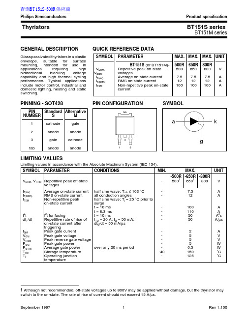
Philips SemiconductorsProduct specificationThyristors BT151S seriesBT151M seriesGENERAL DESCRIPTIONQUICK REFERENCE DATAGlass passivated thyristors in a plastic SYMBOL PARAMETERMAX.MAX.MAX.UNIT envelope,suitable for surface mounting,intended for use in BT151S (or BT151M)-500R 650R 800R applications requiring high V DRM ,Repetitive peak off-state 500650800V bidirectional blocking voltage V RRM voltagescapability and high thermal cycling I T(AV)Average on-state current 7.57.57.5A performance.Typical applications I T(RMS)RMS on-state current121212A include motor control,industrial and I TSMNon-repetitive peak on-state 100100100Adomestic lighting,heating and static currentswitching.PINNING - SOT428PIN CONFIGURATIONSYMBOLLIMITING VALUESLimiting values in accordance with the Absolute Maximum System (IEC 134).SYMBOLPARAMETERCONDITIONSMIN.MAX.UNIT -500R -650R -800R V DRM , V RRM Repetitive peak off-state-50016501800V voltages I T(AV)Average on-state current half sine wave; T mb ≤ 103 ˚C-7.5A I T(RMS)RMS on-state current all conduction angles-12A I TSMNon-repetitive peak half sine wave; T j = 25 ˚C prior to on-state currentsurge t = 10 ms -100A t = 8.3 ms -110A I 2t I 2t for fusingt = 10 ms-50A 2s dI T /dt Repetitive rate of rise of I TM = 20 A; I G = 50 mA;-50A/µs on-state current after dI G /dt = 50 mA/µstriggeringI GM Peak gate current -2A V GM Peak gate voltage-5V V RGM Peak reverse gate voltage -5V P GM Peak gate power -5W P G(AV)Average gate power over any 20 ms period -0.5W T stg Storage temperature -40150˚C T jOperating junction -125˚Ctemperature1 Although not recommended, off-state voltages up to 800V may be applied without damage, but the thyristor may switch to the on-state. The rate of rise of current should not exceed 15 A/µs.查询BT151S-500R供应商THERMAL RESISTANCESSYMBOL PARAMETERCONDITIONSMIN.TYP.MAX.UNIT R th j-mb Thermal resistance-- 1.8K/W junction to mounting base R th j-aThermal resistance pcb (FR4) mounted; footprint as in Fig.14-75-K/Wjunction to ambientSTATIC CHARACTERISTICST j = 25 ˚C unless otherwise stated SYMBOL PARAMETER CONDITIONSMIN.TYP.MAX.UNIT I GT Gate trigger current V D = 12 V; I T = 0.1 A -215mA I L Latching current V D = 12 V; I GT = 0.1 A -1040mA I H Holding current V D = 12 V; I GT = 0.1 A -720mA V T On-state voltage I T = 23 A- 1.4 1.75V V GT Gate trigger voltage V D = 12 V; I T = 0.1 A-0.6 1.5V V D = V DRM(max); I T = 0.1 A; T j = 125 ˚C 0.250.4-V I D , I ROff-state leakage currentV D = V DRM(max); V R = V RRM(max); T j = 125 ˚C-0.10.5mADYNAMIC CHARACTERISTICST j = 25 ˚C unless otherwise stated SYMBOL PARAMETER CONDITIONSMIN.TYP.MAX.UNITdV D /dtCritical rate of rise of V DM = 67% V DRM(max); T j = 125 ˚C;off-state voltage exponential waveform;Gate open circuit50130-V/µs R GK = 100 Ω2001000-V/µs t gt Gate controlled turn-on I TM = 40 A; V D = V DRM(max); I G = 0.1 A;-2-µs timedI G /dt = 5 A/µst qCircuit commutated V D = 67% V DRM(max); T j = 125 ˚C;-70-µsturn-off timeI TM = 20 A; V R = 25 V; dI TM /dt = 30 A/µs;dV D /dt = 50 V/µs; R GK = 100 ΩMECHANICAL DATAMOUNTING INSTRUCTIONSNotes1. Plastic meets UL94 V0 at 1/8".DEFINITIONSData sheet statusObjective specification This data sheet contains target or goal specifications for product development. Preliminary specification This data sheet contains preliminary data; supplementary data may be published later. Product specification This data sheet contains final product specifications.Limiting valuesLimiting values are given in accordance with the Absolute Maximum Rating System (IEC 134). Stress above one or more of the limiting values may cause permanent damage to the device. These are stress ratings only and operation of the device at these or at any other conditions above those given in the Characteristics sections of this specification is not implied. Exposure to limiting values for extended periods may affect device reliability. Application informationWhere application information is given, it is advisory and does not form part of the specification.© Philips Electronics N.V. 1997All rights are reserved. Reproduction in whole or in part is prohibited without the prior written consent of the copyright owner.The information presented in this document does not form part of any quotation or contract, it is believed to be accurate and reliable and may be changed without notice. No liability will be accepted by the publisher for any consequence of its use. Publication thereof does not convey nor imply any license under patent or other industrial or intellectual property rights.LIFE SUPPORT APPLICATIONSThese products are not designed for use in life support appliances, devices or systems where malfunction of these products can be reasonably expected to result in personal injury. Philips customers using or selling these products for use in such applications do so at their own risk and agree to fully indemnify Philips for any damages resulting from such improper use or sale.Copyright © Each Manufacturing Company.All Datasheets cannot be modified without permission.This datasheet has been download from :100% Free DataSheet Search Site.Free Download.No Register.Fast Search System.。
可控硅参数——精选推荐

∙型号VRRM(V)VDRM(V)IT(A)IGT(mA/uA) VGT(V) 封装形式MAC97A6 ≥400 ≥400 0.8 3--5 1 TO-92 SOT-8?MAC97A8 ≥600 ≥600 0.8 3--5 1 TO-92 SOT-8?BT131 ≥600 ≥600 1 3--5 0.8 TO-92BT134 ≥600 ≥600 2 3--6 1.8 TO-126BT136 ≥600 ≥600 4 3--6 1.8 TO-220BT137 ≥600 ≥600 8 10--15 1.8 TO-220BT138 ≥600 ≥600 12 12--15 1.8 TO-220BT139 ≥600 ≥600 16 12--15 1.8 TO-220BT151≥600 ≥600 8 1--12 0.8 TO-220如图:主要应用:通用电机控制,取暖和厨房用具,工业和家庭照明等产品。
可控硅/晶闸管特点:晶闸管是一种可控制的整流管,由门极向阴极送出微小信号电流即可触发单向电流自阳极流向阴极。
正面K-G-A. 管脚排列:K-G-A特点: 玻璃钝化芯片、高灵敏的控制极触发电流,低通态压降用途: 应用于各种万能开关器、小型马达控制器、彩灯控制器、漏电保护器、灯具继电器激励器、逻辑集成电路驱动、大功率可控硅门极驱动、摩托车点火器等线路∙BT169D ≥400 ≥400 0.8 5-120 0.8 TO-92BT169G ≥600 ≥600 0.8 5-120 0.8 TO-92BTB04 ≥600 ≥600 4 10 1.8 TO-220BTA04 ≥600 ≥600 4 10 1.8 TO-220BTA06 ≥600 ≥600 6 5--50 1.8 TO-220BTB06 ≥600 ≥600 6 5--50 1.8 TO-220BTA08 ≥600 ≥600 8 5--50 1.8 TO-220BTB08 ≥600 ≥600 8 5--50 1.8 TO-220BTA10 ≥600 ≥600 10 25--50 1.8 TO-220BTB10 ≥600 ≥600 10 25--50 1.8 TO-220BTA12 ≥600 ≥600 12 10--50 1.8 TO-220∙品名= 12A四象限双向可控硅(TRIACs)☆型号= BTA12-1000B◇电流= 12.0(A)◇电压= 1000(V)◇结温= 125(℃)◇封装形式= TO-220AB◇管脚排列= T1-T2-G 【主要用途】变频电路,调光、调温、调速电路,电扇、洗衣机、饮水机、微波炉、空调等家用电器的控制电路。
BTA16-600B双向可控硅晶闸管应用及详细资料

B T A16-600B双向可控硅晶闸管应用及详细资料BTA16-600B主要参数电流-IT(RMS):电压-VDRM:≥600V触发电流:IGT≤18-25mA脚位排列:T1-T2-G(A1-A2-G);A1主电极,A2主电极,G门极BTA16引脚图附:双向可控硅的检测用万用表电阻R*1Ω挡,用红、黑两表笔分别测任意两引脚间正反向电阻,结果其中两组读数为无穷大。
若一组为数十欧姆时,该组红、黑表所接的两引脚为第一阳极A1和控制极G,另一空脚即为第二阳极A2。
确定A1、G极后,再仔细测量A1、G极间正、反向电阻,读数相对较小的那次测量的黑表笔所接的引脚为第一阳极A1,红表笔所接引脚为控制极G。
将黑表笔接已确定的第二阳极A2,红表笔接第一阳极A1,此时万用表指针不应发生偏转,阻值为无穷大。
再用短接线将A2、G极瞬间短接,给G极加上正向触发电压,A2、A1间阻值约10欧姆左右。
随后断开A2、G间短接线,万用表读数应保持10欧姆左右。
互换红、黑表笔接线,红表笔接第二阳极A2,黑表笔接第一阳极A1。
同样万用表指针应不发生偏转,阻值为无穷大。
用短接线将A2、G极间再次瞬间短接,给G极加上负的触发电压,A1、A2间的阻值也是10欧姆左右。
随后断开A2、G极间短接线,万用表读数应不变,保持在10欧姆左右。
符合以上规律,说明被测双向可控硅未损坏且三个引脚极性判断正确。
检测较大功率可控硅时,需要在万用表黑笔中串接一节干电池,以提高触发电压。
如需提供购买或其它中文技术支持请与我取得联系:公司网址:Email:MSN:。
可控硅模块MTC200A

通态电流临界上升率
门极触发电流 门极触发电压 维持电流 门极不触发电压 热阻抗(结至壳)
测试条件
180°正弦半波,50HZ 单面散 热,Tc=85℃
ITM=600A 门 极 触 发 电 流 幅 值
IGM=1.5A,门极电流上升时间 125
tr≤0.5μs
30
VA=12V,IA=1A
25
0.8
20
VDM=67%VDRM
125
180°正弦半波,单面散热
杭州西整电力电子科技有限公司
Hangzhouxizheng Power electronics technology co. LTD.
IT(AV) VDRM/VRRM IFSM I2t
200A 600~1800V 7.2 KA 259 103A2S
符号
IT(AV)
IT(RMS) VDRM VRRM IDRM IRRM ITSM
I2t VTO RT VTM dv/dt
di/dt
IGT VGT IH VGD Rth(j-c)
参数
通态平均电流
参数值 典型
1600
最大 200 314 1800
单位
A A V
30
mA
7.20 KA
259 103A2S
0.80
V
1.27 mΩ
1.65
V
800 V/μs
100 A/μs
50
180 mA
1.0
2.5
V
100 mA
ABB REB650 Relion 650系列高阻差分保护系统自动化产品文件说明书
REB650 ensures fast fault clearance for all types of internal phase-to-phase and ground-to-earth faults in solidly grounded or low impedance grounded power systems. It can also handle all internal multi-phase faults in isolated or high impedance grounded power systems.
ABB introduces a new, unique and compact solution for high impedance differential protection. The numerical busbar protection REB650 IED (Intelligent Electronic Device) provides its users with a wide variety of application opportunities. Designed primarily for the protection of single busbars with or without sectionalizers in high impedance based applications, it also offers high impedance differential protection for generators, autotransformers, shunt reactors and capacitor banks. Its I/O capability allows you to protect up to three 3-phase high impedance differential protection zones with a single IED.
晶闸管模块MTC500A

MTC500A
0.06 ℃/W
5 0.02
℃/W 4
2500
V
4.0±15%
N·m
5.0±15%
N·m
-40
125 ℃
1470
g
杭州西整电力电子科技有限公司
Hangzhouxizheng Power electronics technology co. LTD.
Ver:XZ0318
MTC500A
matters needing at时务必要加装散热器,需提供良好的通风条件。
2、工作环境温度高于 40℃时,应优化散热通风条件。
3、模块工作后会发热,在设备未断电及模块未完全冷却降温之前,严禁用手触摸模块
的任何部位。
杭州西整电力电子科技有限公司
IT(AV) VDRM/VRRM ITSM I2t
500A 600~1800V 16 KA 1280 103A2S
符号
参数
IT(AV)
IT(RMS) VDRM VRRM IDRM IRRM ITSM
I2t VTO RT VTM dv/dt
通态平均电流
方均根电流 断态重复峰值电压 反向重复峰值电压 断态重复峰值电流 反向重复峰值电流 通态不重复浪涌电流 浪涌电流平均时间积 门槛电压 斜率电阻 通态峰值电压 断态电压临界上升率
Hangzhouxizheng Power electronics technology co. LTD.
Ver:XZ0318
第5页
Ver:XZ0318
第1页
可控硅(晶闸管)模块 Thyristor Module
Rth(j-c)
热阻抗(结至壳)
180°正弦半波,单面散热
t0410可控硅参数

t0410可控硅参数
T0410是一种可控硅,也叫做铰接可控硅(Junction Controlled Thyristor),是一种功率半导体器件。
以下是T0410可控硅的
一些常见参数:
1. 阻断电压(Vdrm):最大允许的反向电压,在该电压下,
可控硅能够阻断电流。
2. 最大正向电流(Itav):可控硅能够承受的最大正向电流。
3. 最大导通电压降(Vtm):在可控硅导通状态下的电压降。
4. 最大功耗(Ptot):可控硅在工作状态下的最大功耗。
5. 静态工作电流(Igt):可控硅进入导通状态所需的门极电流。
6. 额定控制电压(Vgt):可控硅进入导通状态所需的控制电压。
7. 额定关断电压(Vgt-off):可控硅进入关断状态所需的控制电压。
8. 动态工作电流(Ih):可控硅保持导通状态所需的保持电流。
9. 动态关断电流(Id):可控硅进入关断状态所需的关断电流。
10. 动态反向耐受电压(VDRM):可控硅在关断状态下能够
承受的最大反向电压。
这些参数会根据具体的T0410可控硅型号或厂商而有所不同,以上仅为一些常见参数的示例。
在使用T0410可控硅时,需
要根据具体应用需求选择合适的参数值。
BTA16-600B双向可控硅晶闸管应用及详细资料
B T A16-600B双向可控硅晶闸管应用及详细资料(总1页) -CAL-FENGHAI.-(YICAI)-Company One1-CAL-本页仅作为文档封面,使用请直接删除BTA16-600B双向可控硅晶闸管应用及详细资料BTA16-600B 主要参数电流-IT(RMS): 16.0A电压-VDRM: ≥600V触发电流: IGT ≤18-25mA脚位排列: T1-T2-G (A1-A2-G);A1主电极,A2主电极,G门极BTA16引脚图附:双向可控硅的检测用万用表电阻R*1Ω挡,用红、黑两表笔分别测任意两引脚间正反向电阻,结果其中两组读数为无穷大。
若一组为数十欧姆时,该组红、黑表所接的两引脚为第一阳极A1和控制极G,另一空脚即为第二阳极A2。
确定A1、G极后,再仔细测量A1、G极间正、反向电阻,读数相对较小的那次测量的黑表笔所接的引脚为第一阳极A1,红表笔所接引脚为控制极G。
将黑表笔接已确定的第二阳极A2,红表笔接第一阳极A1,此时万用表指针不应发生偏转,阻值为无穷大。
再用短接线将A2、G极瞬间短接,给G极加上正向触发电压,A2、A1间阻值约10欧姆左右。
随后断开A2、G间短接线,万用表读数应保持10欧姆左右。
互换红、黑表笔接线,红表笔接第二阳极A2,黑表笔接第一阳极A1。
同样万用表指针应不发生偏转,阻值为无穷大。
用短接线将A2、G极间再次瞬间短接,给G极加上负的触发电压,A1、A2间的阻值也是10欧姆左右。
随后断开A2、G极间短接线,万用表读数应不变,保持在10欧姆左右。
符合以上规律,说明被测双向可控硅未损坏且三个引脚极性判断正确。
检测较大功率可控硅时,需要在万用表黑笔中串接一节1.5V干电池,以提高触发电压。
如需提供购买或其它中文技术支持请与我取得联系:公司网址:Email:MSN:2。
- 1、下载文档前请自行甄别文档内容的完整性,平台不提供额外的编辑、内容补充、找答案等附加服务。
- 2、"仅部分预览"的文档,不可在线预览部分如存在完整性等问题,可反馈申请退款(可完整预览的文档不适用该条件!)。
- 3、如文档侵犯您的权益,请联系客服反馈,我们会尽快为您处理(人工客服工作时间:9:00-18:30)。
12A SERIES STANDARD
The BT151S-650R SCR is suitable to fit modes of control found in applications such as voltage
regulation circuits for motorbikes,over-voltage crowbar protection,motor control circuits in power tools and kitchen aids , inrush current limiting circuits ,capacitive discharge ignition.The insulated fullpack package allows a back toback configuration.
DESCRIPTION
FEATURES
•Repetitive Peak Off-State Voltage : 650V •R.M.S On-State Current ( I = 12 A )•Low On-State Voltage (1.7V(Max.)@ I )•RoHS Compliant
T(RMS)TM
ABSOLUTE MAXIMUM RATINGS ()
T = 25°C UNLESS OTHERWISE SPECIFIED J SILICON CONTROLLED RECTIFIERS
Symbol Parameter Value Unit I T(RMS)RMS on-state current Tc =109°C 12A I T(AV)Average on-state current
Tc =109°C
7.5A I TSM Non repetitive surge peak on-state current tp =8.3ms
Tj=25°C
132
A tp =10ms
120
I²t I²t Value for fusing
tp =10ms Tj=25°C 72A²S dI/dt Critical rateof rise of on-state current I G =2x I GT ,tr ≤100ns F =60Hz Tj=125°C 50A/µs I GM Peak gate current
tp =20µs
Tj=125°C 2A P G(AV)Average gate power dissipation Tj=125°C
0.5W T stg Storage junction temperature range -40to +150
°C
T j Operating junction temperature range -40to +125
V RGM
Maximum peak reverse gate voltage
5
V
V DRM Repetitive Peak off -State Voltage 650V V RRM Repetitive Peak Reverse Voltage
650
V
ELECTRICAL CHARACTERISTICS ( TC = 25 °C UNLESS OTHERWISE NOTED )
VOLTAGE CURRENT CHARACTERISTIC OF SCR
Symbol Test Conditions
Min.Typ.Max.Unit I GT V D =12V R L =140ohm
-315mA V GT -0.6 1.5V V GD V D =V DRM R L =3.3kohm T j =125°C
--0.2V I H I T =500mA -830mA I L I G =1.2I GT
-1040mA d /d V t V D =67%V DRM Gate open T j =125°C 200400-V/µs V TM I TM =23A t p =380µs T j =25°C -- 1.7V I DRM V D =V DRM
V R =V RRM
T j =25°C --10µA I RRM
T j =125°C --0.5
mA
PACKAGE MECHANICAL DATA TO-252(DPAK)。