HCF4538M013TR中文资料
HCPL-M453中文资料

Small Outline, 5 Lead, High Speed Optocouplers Technical DataHCPL-M452HCPL-M453Features• Surface Mountable• Very Small, Low Profile JEDEC Registered Package Outline• Compatible with Infrared Vapor Phase Reflow and Wave Soldering Processes • Very High Common Mode Transient Immunity:15000 V/µs at V CM = 1500 V Guaranteed (HCPL-M453)• High Speed: 1 Mb/s • TTL Compatible• Guaranteed AC and DC Performance overTemperature: 0°C to 70°C • Open Collector Output • Recognized Under the Component Program of U.L. (File No. E55361) for Dielectric Withstand Proof Test Voltage of 3750 Vac, 1Minute• Lead Free OptionCAUTION: The small device geometries inherent to the design of this bipolar component increase the component's susceptibility to damage from electrostatic discharge (ESD). It is advised that normal static precautions be taken in handling and assembly of this component to prevent damage and/or degradation which may be induced by ESD.The SO-5 JEDEC registered (MO-155) package outline does not require “through holes” in a PCB. This package occupies approximately one-fourth the footprint area of the standard dual-in-line package. The lead profile is designed to be compatible with standard surface mount processes.These diode-transistoroptocouplers use an insulating layer between the light emitting diode and an integrated photon detector to provide electrical insulation between input and output. Separate connections for the photodiode bias and output transistor collector increase the speed up to a hundred timesSO-5 Package Standard DIP SO-8 Package HCPL-M452HCPL-4502HCPL-0452HCPL-M453HCPL-4503HCPL-0453(Note: These devices equivalent to 6N135/6N136 devices but without the base lead.)DescriptionThese small outline high CMR,high speed, diode-transistor opto-couplers are single channel devices in a five lead miniature footprint. They are electrically equivalent to the following Agilent optocouplers:tions. A standard 16 mA TTL sink current through the input LED will provide enough output current for 1 TTL load and a 5.6 k Ω pull-up resistor. CTR of the HCPL-M452 is 19%minimum at I F = 16 mA.over that of a conventional photo-transistor coupler by reducing the base-collector capacitance.The HCPL-M452 is designed for high speed TTL/TTL applica-The HCPL-M453 is an HCPL-M452 with increased common mode transient immunity of 15,000 V/µs minimum at V CM =1500 V guaranteed.Applications• Line Receivers -High common mode transient immunity (>1000V/µs) and low input-output capacitance (0.6 pF).• High Speed Logic Ground Isolation - TTL/TTL, TTL/LTTL, TTL/CMOS, TTL/LSTTL.• Replace Slow Phototran-sistor Optocouplers • Replace PulseTransformers - Save board space and weight• Analog Signal Ground Isolation -Integrated photon detector provides improved linearity over phototransistor type.Land Pattern RecommendationDIMENSIONS IN MILLIMETERS AND (INCHES)Outline Drawing (JEDEC MO-155)SchematicGNDV CCV OANODECATHODEDIMENSIONS IN MILLIMETERS (INCHES)* MAXIMUM MOLD FLASH ON EACH SIDE IS 0.15 mm (0.006)NOTE: FLOATING LEAD PROTRUSION IS 0.15 mm (6 mils) MAX.MAX.= 0.102 (0.004)Absolute Maximum Ratings(No Derating Required up to 85°C)Storage Temperature .................................................-55°C to +125°C Operating Temperature .............................................-55°C to +100°C Average Input Current - I F .....................................................25 mA [1]Peak Input Current - I F ...........................................................50 mA [2](50% duty cycle, 1 ms pulse width)Peak Transient Input Current - I F ..............................................1.0 A(≤1 µs pulse width, 300 pps)Reverse Input Voltage - V R (Pin3-1)...............................................5 V Input Power Dissipation ........................................................45 mW [3]Average Output Current - I O (Pin 5)...........................................8 mA Peak Output Current .................................................................16 mA Output Voltage - V O (Pin 5-4)........................................-0.5 V to 20 V Supply Voltage - V CC (Pin 6-4).......................................-0.5 V to 30 V Output Power Dissipation....................................................100 mW [4]Infrared and Vapor Phase Reflow Temperature..................see belowSolder Reflow Thermal ProfileRecommended Pb-Free IR ProfileTIME (SECONDS)T E M P E R A T U R E (°C )ROOM°C of ACTUAL NOTES:THE TIME FROM 25 °C to PEAK TEMPERATURE = 8 MINUTES MAX.T smax = 200 °C, T smin = 150 °CInsulation Related SpecificationsParameter Symbol Value Units ConditionsMin External Air Gap L(IO1)≥ 5mm Measured from input terminals (Clearance)to output terminalsMin. External Tracking Path L(IO2)≥ 5mm Measured from input terminals (Creepage)to output terminalsMin. Internal Plastic Gap0.08mm Through insulation distance (Clearance)conductor to conductor Tracking Resistance CTI175V DIN IEC 112/VDE 0303 Part 1 Isolation Group (per DIN VDE 0109)IIIa Material Group DIN VDE 0109Electrical SpecificationsOver recommended temperature (T A = 0°C to 70°C) unless otherwise specified. (See note 11.)*All typicals at T A = 25°C.Switching SpecificationsOver recommended temperature (T A = 0°C to 70°C) V CC = 5 V, I F = 16 mA unless otherwise specified.All typicals at T A = 25°C.Notes:1. Derate linearly above 85°C free-air temperature at a rate of 0.5 mA/°C.2. Derate linearly above 85°C free-air temperature at a rate of 1.0 mA/°C.3. Derate linearly above 85°C free-air temperature at a rate of 1.1 mW/°C.4. Derate linearly above 85°C free-air temperature at a rate of 2.3 mW/°C.5. CURRENT TRANSFER RATIO in percent is defined as the ratio of output collector current, I O, to the forward LED inputcurrent, I F, times 100.6. Device considered a two terminal device: pins 1 and 3 shorted together, and pins 4, 5 and 6 shorted together.7. In accordance with UL 1577, each optocoupler is proof tested by applying an insulation test voltage ≥4500 V RMS for 1 second(leakage detection current limit, I I-O≤ 5 µA).8. Common transient immunity in a Logic High level is the maximum tolerable (positive) dV CM/dt on the rising edge of thecommon mode pulse, V CM, to assure that the output will remain in a Logic High state (i.e., V O > 2.0 V). Common mode transient immunity in a Logic Low level is the maximum tolerable (negative) dV CM/dt on the falling edge of the common mode pulse signal, V CM to assure that the output will remain in a Logic Low state (i.e., V O < 0.8 V).9. The 1.9 kΩ load represents 1 TTL unit load of 1.6 mA and the 5.6 kΩ pull-up resistor.10. The frequency at which the ac output voltage is 3 dB below its mid-frequency value.11. Use of a 0.1 µF bypass capacitor connected between pins 4 and 6 is recommended.Figure 7. Logic High Output Current vs. Temperature.Figure 8. Small-Signal CurrentTransfer Ratio vs. Quiescent Input Current.Figure 4. Current Transfer Ratio vs.Temperature.Figure 5. Propagation Delay vs.Temperature.Figure 6. Propagation Delay Time vs. Load Resistance.Figure 1. dc and Pulsed Transfer Characteristics.Figure 2. Current Transfer Ratio vs.Input Current.Figure 3. Input Current vs. Forward Voltage.105V O – OUTPUT VOLTAGE – VI O – O U T P U T C U R R E N T – m A1.51.00.50.1N O R M A L I Z E D C U R R E N T T R A N S F E R R A T I OI F – INPUT CURRENT – mA V F – FORWARD VOLTAGE – VOLTSI F – F O R W A R D C U R R E N T – m A1.11.00.90.80.70.6N O R M A L I Z E D C U R R E N T T R A N S F E R R A T I OT A – TEMPERATURE – °C200015001000500T A – TEMPERATURE – °C t P – P R O P A G A T I O N D E L A Y – n s3.02.01.00.60.40.20.8R L – LOAD RESISTANCE – k Ωt P – P R O P A G A T I O N D E L A Y – µsT A – TEMPERATURE – °C101010100101010I O H – L O G I C H I G H O U T P U T C U R R E N T – n A∆I F ∆I O – S M A L L S I G N A L C U R R E N T T R A N S F E R R A T I O0.100.200.30I F – QUIESCENT INPUT CURRENT – mAFigure 11. Test Circuit for Transient Immunity and Typical Waveforms.Figure 10. Switching Test Circuit.Figure 9. Frequency Response.f – FREQUENCY – MHzN O R M A L I Z E D R E S P O N S E –d BAC INPUTOOI F = 15 pFt V I FOV V 0 VSWITCH AT B: I = 1.6 mA FV CMCCt r , t f = 16 ns/semiconductors For product information and a complete list of distributors, please go to our web site.For technical assistance call:Americas/Canada: +1 (800) 235-0312 or (916) 788-6763Europe: +49 (0) 6441 92460China: 10800 650 0017Hong Kong: (+65) 6756 2394India, Australia, New Zealand: (+65) 6755 1939 Japan: (+81 3) 3335-8152 (Domestic/Interna-tional), or 0120-61-1280 (Domestic Only) Korea: (+65) 6755 1989Singapore, Malaysia, Vietnam, Thailand, Philippines, Indonesia: (+65) 6755 2044 Taiwan: (+65) 6755 1843Data subject to change.Copyright © 2004 Agilent Technologies, Inc. Obsoletes 5989-0792ENDecember 28, 20045989-2117EN。
CD74HC4538中文资料
TEMP. RANGE
PART NUMBER
(oC)
PACKAGE
PKG. NO.
CD54HC4538F
-55 to 125 16 Ld CERDIP F16.3
CD74HC4538E
-55 to 125 16 Ld PDIP
E16.3
CD74HCT4538E
VCC
VCC
RX 2(14)
CX
1(15)
8
VCC
3(13) R
4(12) A
5(11) B
16 VCC
HIGH Z
VCC
D R1 R2 Q
CL FF CL
Q
VCC
R1
+ COMP II
-
R2
VCC
6(10) Q
7(9) Q
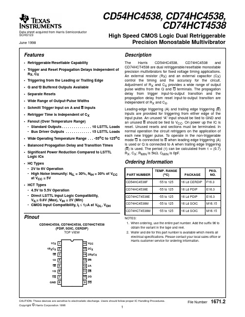
FIGURE 2. LOGIC DIAGRAM (1 MONO)
FUNCTIONAL TERMINAL CONNECTIONS
1
File Number 1671.2
元器件交易网 CD54HC4538, CD74HC4538, CD74HCT4538
Functional Diagram
1Cx 1Rx
1
2
VCC
1Cx 4 1A
1RxCx 6
1Q
5 1B
MONO 1
7 1Q
3 1R
13 2R
12 2A
元器件交易网
Data sheet acquired from Harris Semiconductor SCHS123 June 1998
CD54HC4538, CD74HC4538, CD74HCT4538
4538芯片
4538芯片4538芯片是一款功能强大的定时器芯片,它具有多种应用场景和广泛的潜在用途。
下面将对4538芯片进行详细介绍,包括其工作原理、主要特点和使用方法。
4538芯片采用CMOS技术制造,工作电压范围为3V至18V,工作温度范围为-40°C至85°C。
它内部集成了两个可独立工作的单稳态多谐振荡器,也称为单稳态多谐振荡器。
这款芯片的工作原理基于RC网络和触发器的组合。
RC网络决定了单稳态多谐振荡器的稳态时间,而触发器则触发输出脉冲信号。
4538芯片可以通过改变RC网络的参数来调节输出脉冲信号的频率和宽度。
4538芯片的主要特点如下:1. 较大的频率范围:4538芯片的频率范围可调节从0.1Hz至100kHz,可以满足不同应用的需求。
2. 高精度:由于4538芯片采用了高性能的CMOS技术,其稳态时间可以达到0.01%的精度,能够保证输出信号的准确性。
3. 宽电压范围:4538芯片支持宽电压范围的工作,从3V至18V,适用于多种供电条件。
4. 低功耗:4538芯片采用CMOS技术,具有低功耗特性,可以延长电池寿命。
5. 可编程输出:4538芯片的输出脉冲信号可以通过改变RC网络的参数进行编程,实现不同的输出频率和宽度。
4538芯片的使用方法相对简单,下面是一些基本的步骤:1. 连接电源:将4538芯片的VCC引脚连接到正电源,将GND引脚连接到地。
2. 设置参数:通过改变RC网络的参数来设置输出信号的频率和宽度。
可以通过改变电阻和电容的数值来实现。
3. 连接触发器:将4538芯片的触发器引脚连接到外部触发器,外部触发器可以是按钮、传感器或其他设备。
4. 获得输出:当触发器引脚接收到触发信号时,4538芯片会根据设置的参数生成相应的输出脉冲信号。
总之,4538芯片是一款功能强大且易于使用的定时器芯片,适用于多种应用场景。
它具有广泛的潜在用途,如电子钟、计时器、脉冲产生器等。
无论是在消费电子产品还是工业控制系统中,4538芯片都有着重要的作用。
cd4538芯片资料,中文

终止输出脉冲;不用的 RD 应接 VDD。但整个触发器不用时,器
RD 应接 Vss。
CC4538 提供了 16 引线多层陶瓷双列直插(D)、熔封陶瓷双列
直插(J)、塑料双列直插(P)和陶瓷片状载体(C)4 种封装形式。
推荐工作条件
引出端排列(俯视)
电源电压范围……………….3V~15V
输入电压范围………………..0V~VDD
工作温度范围
M 类……………….-55℃~125℃
E 类……………….-40℃~85℃
极限值 电源电压…...-0.5V~18V 输入电压……-0.5V~VDD+0.5V 输入电流…………….±10mA 储存稳定…………….-65℃~150℃
引出端功能符号
1Cext、2Cext 外接电容端
1Q、2Q
每个触发器具有上升沿触发输入(TR+)和下降沿( TR -),
TR+和 TR -带有施密特触发器,使上升和下降时间不受限制,不
用的 TR+应接 Vss;不用的 TR -应接 VDD。对于非可重触发方式
工作,当采用上升沿触发时(TR+), TR -应接至 Q ;当采用下
降沿触发时( TR -),TR+应接至 Q。直接复位 RD 处于低电平时,
mA µA µA
动态工作条件(TA=25℃) 参数
tw
TR+、 TR -、RD
VDD=5V 最小 最大 170 -
规范值 VDD=10V 最小 最大
90
-
VDD=15V 最小 最大
80
-
脉冲宽度 tr、tf 上升或下 RD
降时间
-
15
-
5
-
4
TR+
无限制
单位 ns µs µs
4538集成电路IC
1/10September 2001sRETRIGGERABLE/RESETTABLE CAPABILITY s TRIGGER AND RESET PROPAGATION DELAYS INDEPENDENT OF R X , C X s TRIGGERING FROM LEADING OR TRAILING EDGE s Q AND Q BUFFERED OUTPUT AVAILABLE s SEPARATE RESETS s WIDE RANGE OF OUTPUT PULSE WIDTHS s QUIESCENT CURRENT SPECIFIED UP TO 20V s 5V, 10V AND 15V PARAMETRIC RATINGS s SCHMITT TRIGGER INPUT ALLOWSUNLIMITED RISE AND FALL TIMES ON +TR AND -TR INPUTS s INPUT LEAKAGE CURRENTI I = 100nA (MAX) AT V DD = 18V T A = 25°C s 100% TESTED FOR QUIESCENT CURRENT s MEETS ALL REQUIREMENTS OF JEDEC JESD13B " STANDARD SPECIFICATIONS FOR DESCRIPTION OF B SERIES CMOS DEVICES"DESCRIPTIONThe HCF4538B is a monolithic integrated circuit fabricated in Metal Oxide Semiconductor technology available in DIP and SOP packages. The HCF4538B dual precision monostable multivibrator provides stable retriggerable/resettable one-shot operation for any fixed voltage timing application. An external resistor (R X ) and an external capacitor (C X ) control the timing and accuracy for the circuit. Adjustment of R X and C X provides a wide range of output pulse widths from the Q and Q terminals. The time delay from trigger input to output transition (trigger propagation delay) and the time delay from reset input to output transition (reset propagation delay) and the time delay from reset input to output transition (reset propagation delay) are independent of R X and C X . Precision control of output pulse width is achieved through linear CMOS techniques.Leading edge triggering (+TR) and trailing edge triggering (-TR) inputs are provided for triggeringHCF4538BDUAL MONOSTABLE MULTIVIBRATORPIN CONNECTIONORDER CODESPACKAGE TUBE T & R DIP HCF4538BEY SOPHCF4538BM1HCF4538M013TRHCF4538B2/10from either edge of an input pulse. An unused +TR input should be tied to V SS . An unused -TR input should be tied to V DD . A RESET (on low level) is provided for immediate termination of the output pulse or to prevent output pulses when power is turned on. An unused RESET input should be tied to V DD . However, if an entire section of the HCF4538B is not used, its inputs must be tied to either V DD or V SS (see table 1). In normal operation the circuit triggers (extends the output pulse one period) on the application of each new trigger pulse. For operation in the non-retiggerable mode, Q is connected to -TR when leading edge triggering (+TR) is used or Q is connected to +TR when trailing edge triggering (-TR) is used. The time period (T) for this multivibrator can be calculated by : T = R X C X . The min. value of external resistance, R X , is 4K Ω. The max. and min. values of external capacitance, C X , are 100µF and 5nF, respectively. IINPUT EQUIVALENT CIRCUITPIN DESCRIPTIONTerminals 1, 8, 15 are electrically connected internallyFUNCTIONAL DIAGRAMPIN No SYMBOL NAME AND FUNCTION 4, 12+TR Trigger Inputs (Low to High, Edge-Triggered)5, 11-TR Trigger Inputs (High to Low, Edge-Triggered)3, 13RESET Direct Reset Inputs (Active Low)1, 15C X 1, C X 2External Capacitor Con-nections2, 14R X C X 1R X C X 2External Resistor/Capaci-tor Connections 6, 10Q1, Q2Pulse Outputs7, 9Q1, Q2Complementary Pulse Outputs8V SS Negative Supply Voltage 16V DDPositive Supply VoltageHCF4538B3/10TABLE 1 : Functional Terminal ConnectionsA Retriggerable one-shot multivibrator has an output pulse width which is extended on full time period (T) after application of the last trigger pulse.A Non-Retriggerable one-shot multivibrator has a time period (T) referenced from the application of the firs trigger pulse.LOGIC DIAGRAMFUNCTIONV DD to Term. N °V SS to Term. N °Input Pulse to Term. N °Other ConnectionsMono (1)Mono (2)Mono (1)Mono (2)Mono (1)Mono (2)Mono (1)Mono (2)Leading Edge Trigger/Retriggerable3, 511, 13412Leading Edge Trigger/NonRetriggerable 3134125, 711, 9Trailing Edge Trigger/Retriggerable313412511Trailing Edge Trigger/NonRetriggerable3135114, 612, 10HCF4538B4/10LOGIC DIAGRAMABSOLUTE MAXIMUM RATINGSAbsolute Maximum Ratings are those values beyond which damage to the device may occur. Functional operation under these conditions is not implied.All voltage values are referred to V SS pin voltage.RECOMMENDED OPERATING CONDITIONSSymbol ParameterValue Unit V DD Supply Voltage-0.5 to +22V V I DC Input Voltage -0.5 to V DD + 0.5V I I DC Input Current± 10mA P D Power Dissipation per Package200mW Power Dissipation per Output Transistor 100mW T op Operating Temperature -55 to +125°C T stgStorage Temperature-65 to +150°CSymbol ParameterValue Unit V DD Supply Voltage 3 to 20V V I Input Voltage0 to V DD V T opOperating Temperature-55 to 125°CHCF4538B5/10DC SPECIFICATIONSThe Noise Margin for both "1" and "0" level is: 1V min. with V DD =5V, 2V min. with V DD =10V, 2.5V min. with V DD =15VSymbolParameterTest ConditionValue UnitV I (V)V O (V)|I O |(µA)V DD (V)T A = 25°C -40 to 85°C -55 to 125°C Min.Typ.Max.Min.Max.Min.Max.I LQuiescent Current0/550.045150150µA0/10100.0410*******/15150.04206006000/20200.0810030003000V OHHigh Level Output Voltage0/5<15 4.95 4.95 4.95V0/10<1109.959.959.950/15<11514.9514.9514.95V OLLow Level Output Voltage5/0<150.050.050.05V10/0<1100.050.050.0515/0<1150.050.050.05V IHHigh Level Input Voltage 0.5/4.5<15 3.5 3.5 3.5V1/9<1107771.5/13.5<115111111V ILLow Level Input Voltage 4.5/0.5<15 1.5 1.5 1.5V9/1<11033313.5/1.5<115444I OHOutput Drive Current0/5 2.5<15-1.6-3.2-1.3-1.3mA0/5 4.6<15-0.51-1-0.42-0.420/109.5<110-1.3-2.6-1.1-1.10/1513.5<115-3.4-6.8-2.8-2.8I OLOutput Sink Current0/50.4<15-0.511-0.42-0.42mA 0/100.5<110-1.3 2.6-1.1-1.10/15 1.5<115-3.46.8-2.8-2.8I I Input Leakage Current0/18Any Input 18±10-5±0.1±1±1µA C IInput CapacitanceAny Input57.5pFHCF4538B6/10DYNAMIC ELECTRICAL CHARACTERISTICS (T amb = 25°C, C L = 50pF, R L = 200K Ω, t r = t f = 20 ns)(*) Typical temperature coefficient for all V DD value is 0.3 %/°C.(1) Minimum R X value = 4K Ω , minimum C X value = 5000 pFSymbolParameterTest ConditionValue (*)UnitV DD (V)Min.Typ.Max.t TLH t THL Transition Time5100200ns 1050100154080t PLH t PHL Propagation Delay Time+TR or -TR to Q or Q 5300600ns1015030015100200t PLH t PHL Propagation Delay TimeReset to Q or Q 5R L = 1K Ω250500ns101252501595190t WH t WLMinimum Input Pulse Width +TR, -TR or Reset 5R L = 1K Ω80140ns104080153060t WTOutput Pulse Width - Q or Q (C X = 0.005 µF, R X = 10K Ω (1))55760.664.5µs105558.963.0155559.163.5t WTOutput Pulse Width - Q or Q (C X = 0.1µF, R X = 100K Ω)59.49.9710.5ms109.49.9510.6159.510.010.6t WTOutput Pulse Width - Q or Q (C X = 10µF, R X = 100K Ω)50.95 1.0 1.06s100.95 1.0 1.06150.961.0 1.07t WPulse Width MatchBetween Circuits in Same Package : (100(T 1 - T 2)/T 1) (C X = 0.1µF, R X = 100K Ω) 5± 1%10± 115± 1t rrMinimum Retrigger Time50ns 100150C INInput CapacitanceAny Input57.5pFHCF4538B7/10TEST CIRCUITLR L = 200K ΩR T = Z OUT of pulse generator (typically 50Ω)WAVEFORM : PROPAGATION DELAY TIMES (f=1MHz; 50% duty cycle)HCF4538BInformation furnished is believed to be accurate and reliable. However, STMicroelectronics assumes no responsibility for the consequences of use of such information nor for any infringement of patents or other rights of third parties which may result from its use. No license is granted by implication or otherwise under any patent or patent rights of STMicroelectronics. Specifications mentioned in this publication are subject to change without notice. This publication supersedes and replaces all information previously supplied. STMicroelectronics products are not authorized for use as critical components in life support devices or systems without express written approval of STMicroelectronics.© The ST logo is a registered trademark of STMicroelectronics© 2001 STMicroelectronics - Printed in Italy - All Rights ReservedSTMicroelectronics GROUP OF COMPANIESAustralia - Brazil - China - Finland - France - Germany - Hong Kong - India - Italy - Japan - Malaysia - Malta - MoroccoSingapore - Spain - Sweden - Switzerland - United Kingdom© 10/10。
74HC4538中文资料

GENERAL DESCRIPTION
The 74HC/HCT4538 are high-speed Si-gate CMOS devices and are pin compatible with “4538” of the “4000B” series. They are specified in compliance with JEDEC standard no. 7A.
Product specification
74HC/HCT4538
Fig.1 Pin configuration.
Fig.2 Logic symbol.
Fig.3 IEC logic symbol.
September 1993
3
元器件交易网
Philips Semiconductors
Philips Semiconductors
Dual retriggerable precision monostable multivibrator
Product specification
74HC/HCT4538
FEATURES
• Separate reset inputs • Triggering from leading or trailing edge • Output capability: standard • ICC category: MSI • Power-on reset on-chip
CH453手册

CH453 中文手册
3
5.3. 键盘扫描
CH453 的键盘扫描功能支持 8×8 矩阵的 64 键键盘。在键盘扫描期间,DIG7~DIG0 引脚用于列 扫描输出,SEG7~SEG0 引脚都带有内部下拉电阻,用于行扫描输入。
CH453 定期在显示驱动扫描过程中插入键盘扫描。在键盘扫描期间,DIG7~DIG0 引脚按照 DIG0 至 DIG7 的顺序依次输出高电平,其余引脚输出低电平;SEG7~SEG0 引脚的输出被禁止,当没有键被 按下时,SEG7~SEG0 都被下拉为低电平;当有键被按下时,例如连接 DIG3 与 SEG4 的键被按下,则 当 DIG3 输出高电平时 SEG4 检测到高电平;为了防止因为按键抖动或者外界干扰而产生误码,CH453 实行两次扫描,只有当两次键盘扫描的结果相同时,按键才会被确认有效。如果 CH453 检测到有效的 按键,则记录下该按键代码,并通过 INT#引脚产生低电平有效的键盘中断,此时单片机可以通过串 行接口读取按键代码;在没有检测到新的有效按键之前,CH453 不再产生任何键盘中断。CH453 不支 持组合键,也就是说,同一时刻,不能有两个或者更多的键被按下;如果多个键同时按下,那么按键 代码较小的按键优先。
CH453 所提供的按键代码为 7 位,位 2~位 0 是列扫描码,位 5~位 3 是行扫描码,位 6 是状态 码(键按下为 1,键释放为 0)。例如,连接 DIG3 与 SEG4 的键被按下,则按键代码是 1100011B 或者 63H,键被释放后,按键代码通常是 0100011B 或者 23H(也可能是其它值,但是肯定小于 40H),其中, 对应 DIG3 的列扫描码为 011B,对应 SEG4 的行扫描码为 100B。单片机可以在任何时候读取按键代码, 但一般在 CH453 检测到有效按键而产生键盘中断时读取按键代码,此时按键代码的位 6 总是 1,另外, 如果需要了解按键何时释放,单片机可以通过查询方式定期读取按键代码,直到按键代码的位 6 为 0。
ioThinx 4530 Series硬件用户手册说明书

ioThinx 4530 Series HardwareUser’s ManualVersion 1.1, August 2019/product© 2019 Moxa Inc. All rights reserved.ioThinx 4530 Series HardwareUser’s ManualThe software described in this manual is furnished under a license agreement and may be used only in accordance withthe terms of that agreement.Copyright Notice© 2019 Moxa Inc. All rights reserved.TrademarksThe MOXA logo is a registered trademark of Moxa Inc.All other trademarks or registered marks in this manual belong to their respective manufacturers.DisclaimerInformation in this document is subject to change without notice and does not represent a commitment on the part of Moxa.Moxa provides this document as is, without warranty of any kind, either expressed or implied, including, but not limited to, its particular purpose. Moxa reserves the right to make improvements and/or changes to this manual, or to the products and/or the programs described in this manual, at any time.Information provided in this manual is intended to be accurate and reliable. However, Moxa assumes no responsibility for its use, or for any infringements on the rights of third parties that may result from its use.This product might include unintentional technical or typographical errors. Changes are periodically made to the information herein to correct such errors, and these changes are incorporated into new editions of the publication.Technical Support Contact Information/supportMoxa AmericasToll-free: 1-888-669-2872 Tel: +1-714-528-6777 Fax: +1-714-528-6778Moxa China (Shanghai office) Toll-free: 800-820-5036Tel: +86-21-5258-9955 Fax: +86-21-5258-5505Moxa EuropeTel: +49-89-3 70 03 99-0 Fax: +49-89-3 70 03 99-99Moxa Asia-PacificTel: +886-2-8919-1230 Fax: +886-2-8919-1231Moxa IndiaTel: +91-80-4172-9088 Fax: +91-80-4132-1045Safety SymbolsNOTE Indicates a potential malfunction which, if not avoided, will not result in damage to property. INFORMATION This information is important for preventing errors.Table of Contents1.Preface .............................................................................................................................................. 1-1Revision History ................................................................................................................................. 1-2 Relevant Models ................................................................................................................................. 1-2 Package Contents ............................................................................................................................... 1-2 Usage Scenarios ................................................................................................................................. 1-2 Hardware and Software Requirements ................................................................................................... 1-3 Safety Precautions .............................................................................................................................. 1-3 Additional Resources ........................................................................................................................... 1-4 2.Product Overview .............................................................................................................................. 2-1Specifications ..................................................................................................................................... 2-2 Appearance ........................................................................................................................................ 2-2 Front View .................................................................................................................................. 2-2Physical Dimensions .................................................................................................................... 2-2 LED Indicators .................................................................................................................................... 2-3 3.Hardware Installation ....................................................................................................................... 3-1Wiring System and Field Power ............................................................................................................. 3-2 System Power ............................................................................................................................. 3-2Field Power ................................................................................................................................. 3-3 Wiring Ethernet Ports .......................................................................................................................... 3-3 Wiring Serial Port(s) ............................................................................................................................ 3-4 Serial Console (Debug Port) ................................................................................................................. 3-5 Grounding the Unit ............................................................................................................................. 3-8 Connecting the System Power Ground ........................................................................................... 3-8Connecting the Field Power Ground ............................................................................................... 3-8 Mounting the Unit ............................................................................................................................... 3-9 Installing the Unit on a DIN Rail .................................................................................................... 3-9Removing the Unit from a DIN Rail .............................................................................................. 3-10Installing Covers on the Device and the Right-Most I/O Module ....................................................... 3-11Removing a Cover from the Right-Most Module ............................................................................. 3-11Horizontal Installation ................................................................................................................ 3-12 Powering on the Unit ......................................................................................................................... 3-12 Reset Button: Factory Reset Process ................................................................................................... 3-121PrefaceIn this chapter, we explain the scope of and how to use this document.The following topics are covered in this chapter:❒Revision History❒Relevant Models❒Package Contents❒Usage Scenarios❒Hardware and Software Requirements❒Safety Precautions❒Additional ResourcesRevision HistoryVersion Change DateV1.0 First Release 2019-01-25Relevant ModelsThis document is only applicable to the models listed below.Model Name DescriptionioThinx 4533-LX Controller with Cortex-A7 1 GHz dual-core CPU, 512 MB RAM, 3-in-1 serial ports, LinuxOS, -20 to 60°C operating temperatureioThinx 4533-LX-T Controller with Cortex-A7 1 GHz dual-core CPU, 512 MB RAM, 3-in-1 serial ports, LinuxOS, -40 to 75°C operating temperaturePackage ContentsThe following items are included in the product package.•The ioThinx 4530 Series device•Quick installation guide (Printed)•Warranty cardUsage ScenariosThe ioThinx 4530 Series advanced controllers have the high computing power required to easily and securely upload field site data to the cloud. For cloud connectivity, the ioThinx 4530 comes with Azure, AWS, and Alibaba Cloud SDKs pre-installed.Users can take advantage of the built-in cloud examples, removing dependency on the libraries and toolchain configurations. For better control precision, the Moxa Industrial Linux operating system gives the ioThinx 4530 Series the capability to handle computations and control actions at the same time. In addition, the ioThinx 4530 Series helps manage data privacy, and supports both hardware privacy features, such as TPM (TrustedPlatform Module, which is optional), and software privacy features, such as secure boot, to help usersimplement cybersecurity protections. For users who are not proficient at using typical PLC programminglanguages, the ioThinx 4530 series supports C/C++ and Python, both of which provide more advancedprogramming options, to help users easily build their own applications.Hardware and Software Requirements You will need the following hardware and software to use the ioThinx 4530 Series.• A power source that provides 12 to 48 VDC, and power wires• A PC running Linux OS (we recommend Debian 9, Kernel 4.4) and an Ethernet cable•45MR/ML modules, if availableSafety PrecautionsPlease observe the following safety precautions when installing and using the ioThinx 4510 Series:Additional ResourcesRefer to the following documents for additional information.•Datasheets for the following products:ioThinx 4530 SeriesioThinx 4500 Series (45MR/ML) Modules•User’s Manual for the following products:ioThinx 4500 (45M) Module Series2Product OverviewIn this chapter, we give an overview of each ioThinx 4530 Series product.The following topics are covered in this chapter:❒Technical DataCommon Specifications❒AppearanceFront ViewPhysical Dimensions❒LED IndicatorsioThinx 4530 Series Hardware Product Overview SpecificationsNOTE The latest specifications for Moxa’s products can be found at https://. AppearanceFront ViewPhysical DimensionsioThinx 4530 Series Hardware Product Overview LED IndicatorsLabel Usage Qty Color ActionSP System Power 1 Green On: Power onOff: Power offFP Field Power 1 Green On: Power onOff: Power offRDY System (kernel) 1 Green/Red Green: System readyGreen (blinking): System is booting upRed: System error, or executing factorydefaultRed (blinking): Triggering factory default,or upgrading the firmware U1/U2 User defined 1 of each Green/Red User-definedSD microSD card 1 Green Green: SD card is insertedOFF: SD card is being accessedL1/L2 Ethernet 1 of each Green/Amber Green: 100MbAmber: 10MbBlinking: Data is being transmitted Off: InactiveP1/P2 Serial 1 of each Green/Amber Green: TxAmber: RxBlinking: Data is being transmitted Off: InactiveNOTE DO NOT DISCONNECT THE POWER OR NETWORK CABLE when the RDY LED is blinking.3Hardware InstallationIn this chapter, we describe how to install ioThinx 4530 Series products.The following topics are covered in this chapter:❒Wiring System and Field PowerSystem PowerField Power❒Wiring Ethernet Ports❒Wiring Serial Port(s)❒Serial Console (Debug Port)❒Grounding the UnitConnecting the System Power GroundConnecting the Field Power Ground❒Mounting the UnitInstalling the Unit on a DIN RailRemoving the Unit from a DIN RailInstalling Covers on the Device and the Right-Most I/O ModuleRemoving a Cover from the Right-Most ModuleHorizontal Installation❒Powering on the Unit❒Reset Button: Factory Reset ProcessWiring System and Field PowerWire range: 12 to 26 AWG (Ferrule diameter: 2.0 to 0.4 mm) Wire strip length: 10 mm Unit: mm (in.)NOTEPowering the unit requires connecting both the system and field power to the power supply. If only one of the power sources is connected, the device may not work properly.NOTEWe recommended using different power supplies to ensure that the system power and field power are isolated from each other. If using the same power supply for system power and field power, 3 KV or above isolation between them is recommended.System PowerThis device requires a 12 to 48 VDC system power input. The system power powers this device and the expansion modules via an internal bus, which is galvanically connected to the system power supply.The amount of system current required to support an expansion module is 1 A. If more modules and more power consumption is needed, an additional power module (45MR-7210) is required. Below is an example: • 10 x 45MR-1600 (59.4 mA) = 594 mA • 5 x 45MR-3810 (187 mA) = 935 mAThe total system current is 1.594 A, which is greater than 1 A. Therefore, an additional 45MR-7210 is needed.NOTE Install the 45MR-7210 to the left hand side of the module where the power consumption would be exceeded.NOTEWhen booting up the device in a low temperature environment, it may take up to two minutes until the device is up and running.NOTETo avoid damaging your devices, reset all power supplies connected to this device and 45MR-7210 modules at the same time.NOTEClick the following link to see how many 45MR-7210 power modules you will need to support your ioThinx 4500 Series project: Field PowerThis device provides 12/24 VDC field power input, which is a passive power supply without protection and the maximum current output is 2 A.NOTEThe 12/24 VDC field power supply can be connected directly to 45MR modules. If more connection points are needed, purchase 45MR-7820 (8 x FP+ and 8 x FP-) modules.Wiring Ethernet PortsThe maximum cable length of a 10/100BaseT connection is usually stated as 100 m (350 feet), but the actual limit for your application could be longer or shorter depending on the amount of electrical noise in the environment. To minimize the amount of noise, Ethernet cables should not run parallel to power cables or other types of cables that generate electrical noise. The following diagram and table shows the pin assignments for the RJ45 Ethernet ports:PinMedia Direct Interface Signal 1 Tx+ (transmit) 2 Tx- (transmit) 3 Rx+ (receive) 4 Not used 5 Not used 6 Rx- (receive) 7 Not used 8Not usedWiring Serial Port(s)Wire range: 16 to 28 AWG (Ferrule diameter: 1.2 to 0.3 mm) Wire strip length: 9.0 mm Unit: mm (in.)Pin RS-232 RS-422 RS-485 (P1/P2) 1 TXD TXD+ DATA1+ 2 RXDTXD- DATA1- 3 RTS RXD+ DATA2+ 4 CTS RXD- DATA2- 5GNDGNDGNDNOTEConnect the signal common pin (e.g. GND pin on the serial port pin assignment) between each of the serial device units. For insulated wire (shielding cable) that is used to reduce electrical noise, connect the cable shield drain wire to the chassis ground.NOTETo ensure that wires are securely connected to terminal block connectors, strip 7 to 9 mm of insulation off the ends of the wires before connecting them to the terminal block.Serial Console (Debug Port)The serial console gives users a convenient way of connecting to the programmable controllers. This method is particularly useful when using the computer for the first time. The serial console is also effective for connecting to the Moxa programmable controllers when you do not know target network settings and IP addresses.Step 1:Open the card coverConsole port for the ioThinx SeriesStep 2:Attach the 4-pin serial console cable to the console port. The following diagram shows the 4-pin serial connector and pin connections.Pin Assignment for the Serial Console PortSerial Console Default SettingsPin Definition 1 TxD 2RxD 3NC 4GNDParameter Value Baudrate 115200 bps Parity None Data bits 8 Stop bits 1 Flow Control None TerminalVT100We recommend using Moxa PComm Terminal Emulator to connect to the serial console. The following steps describe how to connect the console.1. Download Moxa PComm Lite from the Moxa website ( ).2. Install Moxa PComm Lite to the host Windows PC.3. Run PComm Lite Terminal Emulator from Start → Programs → PComm Lite Ver 1.x → TerminalEmulator .4.Click Profile Open.5.Specify which COM port is connecting to the Moxa controller, and then use the following configurationsettings: 115200, 8, none, 1.6.Click on the Terminal tab and configure the Terminal Type to VT100. Click OK to proceed.7.The serial console will be displayed on the terminal screen.Grounding the UnitThis device has two ground pins. One pin is for system power and the other pin is for field power. Connecting the System Power GroundThe system power ground connector is at the back of the unit. Once the device has been installed on a DIN rail, the system power ground connector will connect to the DIN rail.Connecting the Field Power GroundConnect the field power ground pin () to your field power ground.Mounting the UnitIn this section, we describe how to mount the device on a DIN rail and how to unmount the device from a DINrail.Installing the Unit on a DIN RailTake the following steps to install the unit on a DIN rail.Step 1: Hook the mounting clip of the unit onto the DIN rail, and then lower the clip onto the DIN rail. At least 55 mm of space above the DIN rail should be kept free to ensure that the installation can be done correctly.Step 2: Push the unit towards the DIN rail until the end of the mounting clip snaps into place.INFORMATION When the I/O module is inserted into the correct position, the connection between the internal bus and the previous module is established.Removing the Unit from a DIN RailTake the following steps to remove the unit from a DIN rail.Step 1: Use your finger to pull the release tab on the lower part of the module.Step 2: Press the release tab (item 1 in the figure) and then remove the CPU module from the DIN rail (item2 in the figure).NOTE Disconnect all connections, including Ethernet, serial, and power cables, from the device before removing the device from the DIN rail.Installing Covers on the Device and the Right-Most I/O ModuleInsert the covers on the left side of the device and on the right side of the I/O module that is installed furthest to the right. Make sure the covers cover the internal bus of the module.NOTE The covers provide protection against electrostatic discharge.Removing a Cover from the Right-Most ModuleBefore adding a new module to the right-most module, remove the cover first. Place your hand on the cover and slide it up as indicated in the diagram below.Horizontal InstallationBefore installing the device, ensure there is enough Array space around the device so that it can dissipate heat. Inorder to ensure the device works properly, we suggestreserving the space shown in the figure below.Powering on the UnitAfter turning on the power supply, it will take 5 to 10 seconds for the operating system to boot up. The greenReady LED will illuminate continuously until the operating system is ready.Reset Button: Factory Reset ProcessUse the following procedure to reset the ioThinx to the factory defaults. Note that when you reset the ioThinx,all of your tag definitions, software programs, and files will be deleted, and the service and runtime engine willbe restarted.1.Power off the device.2.Press and hold the reset button; while holding the reset button:a.Power on the device; the RDY LED will blink green while the device is booting up.b.After the device has booted up, the RDY LED will blink red; continue holding the reset button until theRDY LED stops blinking.3.Release the reset button to load the factory default settings.NOTE Do NOT power off, operate, or connect any devices when the RDY LED is a solid red. The factory reset functionis only activated when the system is booting up.NOTE It should take about 20 seconds from the time the RDY LED starts blinking green until it stops blinking red.。
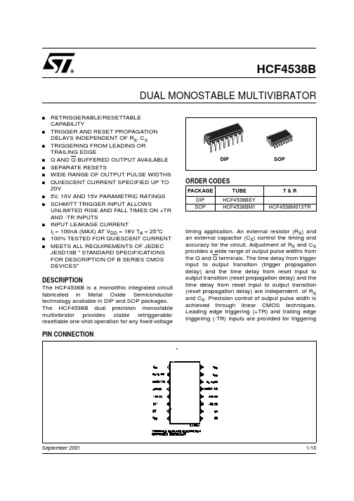
HCF4538B

s RETRIGGERABLE/RESETT ABLECAPABILITYs TRIGGER AND RESET PROPAGATION DELAYS INDEPENDENT OF R X,C Xs TRIGGERING FROM LEADING ORTRAILING EDGEs Q AND Q BUFFERED OUTPUT AVAILABLE s SEPARATE RESETSs WIDE RANGE OF OUTPUT PULSE WIDTHS s QUIESCENT CURRENT SPECIFIED UP TO 20Vs5V,10V AND15V PARAMETRIC RATINGSs SCHMITT TRIGGER INPUT ALLOWS UNLIMITED RISE AND FALL TIMES ON+TR AND-TR INPUTSs INPUT LEAKAGE CURRENTI I=100nA(MAX)AT V DD=18V T A=25°Cs100%TESTED FOR QUIESCENT CURRENT s MEETS ALL REQUIREMENTS OF JEDEC JESD13B”STANDARD SPECIFICATIONSFOR DESCRIPTION OF B SERIES CMOSDEVICES”DESCRIPTIONThe HCF4538B is a monolithic integrated circuit fabricated in Metal Oxide Semiconductor technology available in DIP and SOP packages. The HCF4538B dual precision monostable multivibrator provides stable retriggerable/ resettable one-shot operation for any fixed voltage timing application.An external resistor(R X)and an external capacitor(C X)control the timing and accuracy for the circuit.Adjustment of R X and C X provides a wide range of output pulse widths from the Q and Q terminals.The time delay from trigger input to output transition(trigger propagation delay)and the time delay from reset input to output transition(reset propagation delay)and the time delay from reset input to output transition (reset propagation delay)are independent of R X and C X.Precision control of output pulse width is achieved through linear CMOS techniques. Leading edge triggering(+TR)and trailing edge triggering(-TR)inputs are provided for triggeringHCF4538BDUAL MONOSTABLE MULTIVIBRATORPIN CONNECTION ORDER CODESPACKAGE TUBE T&R DIP HCF4538BEYSOP HCF4538BM1HCF4538M013TRDIP SOP1/10September2001HCF4538B2/10from either edge of an input pulse.An unused +TR input should be tied to V SS .An unused -TR input should be tied to V DD .A RESET (on low level)is provided for immediate termination of the output pulse or to prevent output pulses when power is turned on.An unused RESET input should be tied to V DD .However,if an entire section of the HCF4538B is not used,its inputs must be tied to either V DD or V SS (see table 1).In normal operation the circuit triggers (extends the output pulse one period)on the application of each new trigger pulse.For operation in the non-retiggerable mode,Q is connected to -TR when leading edge triggering (+TR)is used or Q is connected to +TR when trailing edge triggering (-TR)is used.The time period (T)for this multivibrator can be calculated by :T =R X C X .The min.value of external resistance,R X ,is 4K Ω.The max.and min.values of external capacitance,C X ,are 100µF and 5nF,respectively.IINPUT EQUIVALENT CIRCUITPIN DESCRIPTIONTerminals 1,8,15are electrically connected internallyFUNCTIONAL DIAGRAMPIN No SYMBOL NAME AND FUNCTION 4,12+TR Trigger Inputs (Low to High,Edge-Triggered)5,11-TR Trigger Inputs (High to Low,Edge-Triggered)3,13RESET Direct Reset Inputs (Active Low)1,15C X 1,C X 2External Capacitor Con-nections2,14R X C X 1R X C X 2External Resistor/Capaci-tor Connections 6,10Q1,Q2Pulse Outputs7,9Q1,Q2Complementary Pulse Outputs8V SS Negative Supply Voltage 16V DDPositive Supply VoltageHCF4538B3/10TABLE 1:Functional Terminal ConnectionsA Retriggerable one-shot multivibrator has an output pulse width which is extended on full time period (T)after application of the last trigger pulse.A Non-Retriggerable one-shot multivibrator has a time period (T)referenced from the application of the firs trigger pulse.LOGIC DIAGRAMFUNCTIONV DD to Term.N °V SS to Term.N °Input Pulse to Term.N °Other ConnectionsMono (1)Mono (2)Mono (1)Mono (2)Mono (1)Mono (2)Mono (1)Mono (2)Leading Edge Trigger/Retriggerable3,511,13412Leading Edge Trigger/NonRetriggerable 3134125,711,9Trailing Edge Trigger/Retriggerable313412511Trailing Edge Trigger/NonRetriggerable3135114,612,10HCF4538B4/10LOGIC DIAGRAMABSOLUTE MAXIMUM RATINGSAbsolute Maximum Ratings are those values beyond which damage to the device may occur.Functional operation under these conditions is not implied.All voltage values are referred to V SS pin voltage.RECOMMENDED OPERATING CONDITIONSSymbol ParameterValue Unit V DD Supply Voltage -0.5to +22V V I DC Input Voltage -0.5to V DD +0.5V I I DC Input Current±10mA P D Power Dissipation per Package200mW Power Dissipation per Output Transistor 100mW T op Operating Temperature -55to +125°C T stgStorage Temperature-65to +150°CSymbol ParameterValue Unit V DD Supply Voltage 3to 20V V I Input Voltage0to V DD V T opOperating Temperature-55to 125°CHCF4538B5/10DC SPECIFICATIONSThe Noise Margin for both ”1”and ”0”level is:1V min.with V DD =5V,2V min.with V DD =10V,2.5V min.with V DD =15VSymbolParameterTest ConditionValue UnitV I (V)V O (V)|I O |(µA)V DD (V)T A =25°C -40to 85°C -55to 125°C Min.Typ.Max.Min.Max.Min.Max.I LQuiescent Current0/550.045150150µA0/10100.0410*******/15150.04206006000/20200.0810030003000V OHHigh Level Output Voltage0/5<15 4.95 4.95 4.95V0/10<1109.959.959.950/15<11514.9514.9514.95V OLLow Level Output Voltage 5/0<150.050.050.05V10/0<1100.050.050.0515/0<1150.050.050.05V IHHigh Level Input Voltage 0.5/4.5<15 3.5 3.5 3.5V1/9<1107771.5/13.5<115111111V ILLow Level Input Voltage 4.5/0.5<15 1.5 1.5 1.5V9/1<11033313.5/1.5<115444I OHOutput Drive Current0/5 2.5<15-1.6-3.2-1.3-1.3mA0/5 4.6<15-0.51-1-0.42-0.420/109.5<110-1.3-2.6-1.1-1.10/1513.5<115-3.4-6.8-2.8-2.8I OLOutput Sink Current0/50.4<15-0.511-0.42-0.42mA 0/100.5<110-1.3 2.6-1.1-1.10/15 1.5<115-3.46.8-2.8-2.8I I Input Leakage Current0/18Any Input 18±10-5±0.1±1±1µA C IInput CapacitanceAny Input57.5pFHCF4538B6/10DYNAMIC ELECTRICAL CHARACTERISTICS (T amb =25°C,C L =50pF,R L =200K Ω,t r =t f =20ns)(*)Typical temperature coefficient for all V DD value is 0.3%/°C.(1)Minimum R X value =4K Ω,minimum C X value =5000pFSymbolParameterTest ConditionValue (*)UnitV DD (V)Min.Typ.Max.t TLH t THL Transition Time5100200ns 1050100154080t PLH t PHL Propagation Delay Time+TR or -TR to Q or Q 5300600ns1015030015100200t PLH t PHL Propagation Delay TimeReset to Q or Q 5R L =1K Ω250500ns101252501595190t WH t WLMinimum Input Pulse Width +TR,-TR or Reset 5R L =1K Ω80140ns104080153060t WTOutput Pulse Width -Q or Q (C X =0.005µF,R X =10K Ω(1))55760.664.5µs105558.963.0155559.163.5t WTOutput Pulse Width -Q or Q (C X =0.1µF,R X =100K Ω)59.49.9710.5ms109.49.9510.6159.510.010.6t WTOutput Pulse Width -Q or Q (C X =10µF,R X =100K Ω)50.95 1.0 1.06s100.95 1.0 1.06150.961.0 1.07t WPulse Width MatchBetween Circuits in Same Package :(100(T 1-T 2)/T 1)(C X =0.1µF,R X =100K Ω) 5±1%10±115±1t rrMinimum Retrigger Time50ns 100150C INInput CapacitanceAny Input57.5pFHCF4538B7/10TEST CIRCUITC L =50pF or equivalent (includes jig and probe capacitance)R L =200K ΩR T =Z OUT of pulse generator (typically 50Ω)WAVEFORM :PROPAGATION DELAY TIMES (f=1MHz;50%duty cycle)HCF4538B8/10DIM.mm.inchMIN.TYP MAX.MIN.TYP.MAX. a10.510.020B0.77 1.650.0300.065 b0.50.020b10.250.010D200.787 E8.50.335e 2.540.100e317.780.700F7.10.280 I 5.10.201 L 3.30.130Z 1.270.050Plastic DIP-16(0.25)MECHANICAL DATAP001CHCF4538B9/10DIM.mm.inch MIN.TYPMAX.MIN.TYP.MAX.A 1.750.068a10.10.20.0030.007a2 1.650.064b 0.350.460.0130.018b10.190.250.0070.010C 0.50.019c145°(typ.)D 9.8100.3850.393E 5.86.20.2280.244e 1.270.050e38.890.350F 3.8 4.00.1490.157G 4.6 5.30.1810.208L 0.5 1.270.0190.050M 0.620.024S8°(max.)SO-16MECHANICAL DATAPO13HHCF4538BInformation furnished is believed to be accurate and reliable.However,STMicroelectronics assumes no responsibility for the consequences of use of such information nor for any infringe ment of patents or other rights of third parties which may result from its use.No license is granted by implication or otherwise under any patent or patent rights of STMicroelectronics.Specifications mentioned in this publication are subject to change without notice.This publication supersedes and replaces all information previously supplied.STMicroelectronics products are not authorized for use as critical components in life support devices or systems without express written approval of STMicroelectronics.©The ST logo is a registered trademark of STMicroelectronics©2001STMicroelectronics-Printed in Italy-All Rights ReservedSTMicroelectronics GROUP OF COMPANIESAustralia-Brazil-China-Finland-France-Germany-Hong Kong-India-Italy-Japan-Malaysia-Malta-MoroccoSingapore-Spain-Sweden-Switzerland-United Kingdom©http://w 10/10。
4532集成电路IC
8-BIT PRIORITY ENCODER
s CONVERTS FROM 1 TO 8 TO INPUTS BINARY
s PROVIDES CASCADING FEATURE TO HANDLE ANY NUMBER OF INPUTS
s GROUP SELECT INDICATES ONE OR MORE PRIORITY INPUTS
±10-5 ±0.1
±1
±1 µA
CI Input Capacitance
Any Input
5 7.5
pF
The Noise Margin for both "1" and "0" level is: 1V min. with VDD=5V, 2V min. with VDD=10V, 2.5V min. with VDD=15V
H
L
H
L
L
L
L
L
H
X
X
H
L
H
L
L
H
L
L
L
L
L
L
H
X
H
L
L
H
L
H
L
L
L
L
L
L
L
H
H
L
L
L
L
X : Don’t Care
2/11
LOGIC DIAGRAM
HCF4532B
ABSOLUTE MAXIMUM RATINGS
Symbol
Parameter
Value
Unit
VDD Supply Voltage
X : Don’t Care
M54HC4538中文资料

M54HC4538M74HC4538October 1993DUAL RETRIGGERABLE MONOSTABLE MULTIVIBRATORB1R(Plastic Package)ORDER CODES :M54HC4538F1R M74HC4538M1R M74HC4538B1R M74HC4538C1RF1R(Ceramic Package)M1R(Micro Package)C1R (Chip Carrier)PIN CONNECTIONS (top view)NC =No Internal Connecti o n.HIGH SPEEDt PD =25ns (TYP.)AT V CC =5V .LOW POWER DISSIPATIONSTANDBY STATEI CC =4µA (MAX.)AT T A =25°C ACTIVE STATE I CC =200µA (TYP.)AT V CC =5V .HIGH NOISE IMMUNITYV NIH =V NIL =28%V CC (MIN.).OUTPUT DRIVE CAPABILITY 10LSTTL LOADS.BALANCED PROPAGATION DELAYS t PLH =t PHL.WIDE OUTPUT PULSE WIDTH RANGE t WOUT =120ns ~60s OVER AT V CC =4.5V .OUTPUT PULSE WIDTH INDEPENDENT FROM TRIGGER INPUT PULSE WIDTH .PIN AND FUNCTION COMPATIBLE WITH 4538BThe M54/74HC4538is a high speed CMOS DUAL MONOSTABLEMULTIVIBRATOR fabricated in sili-con gate C 2MOS technology.It has the same high speed performance of LSTTL combined with true CMOS low power consumption.Each multivibrator features both a negative,A,and a positive,B,edge triggered input,either of which can be used as an in-hibit input.Also included is a clear input that when taken low resets the one shot.The monostable multivibrators are retriggerable.That is,they may be triggered reapeatedly while their outputs are gener-ating a pulse and the pulse will be extended.Pulse width stability over a wide range of temperature and supply is achieved using linear CMOS techniques.The output pulse equation is simply :PW =0.7(R)(C)where PW is in seconds,R in Ohms,and C is in Farads.All inputs are equipp ed with protection circuits against static discharge and transient excess volt-age.DESCRIPTION1/14M54/M74HC4538 SYSTEM DIAGRAMTIMING CHART2/14BLOCK DIAGRAMNotes:1.Cx,Rx,Dx are extern al comp onen ts.2.Dx is a clamp ing diode.3.The external capaci t or is charg ed to V CC in the stand-by state,i.e.no trigger.When the supp ly voltage is turned off Cx is discharge dmainlythroug h aninternal parasitic diode(see figures).IfCx is sufficiently largeandV CC dec rease s rapidy,there willbesome possibility of damag ing the I.C.with a surge current or latch-up.If the voltage supply filter capacit or is large enoug h and V CC decreas e slowly, the surge curren t is automatically limited and damag e the I.C.is avoided.The maximum forward current of the para sitic diode is ap-proxima tely20mA.In cases where Cx is large the time taken for the suppl y voltage to fall to0.4V CC can be calculated as follows: t f≥(V CC–0.7)⋅Cx/20mAIn cases where t f is too short an external champ ing diode is required to protect the I.C.from the surge curren t. FUNCTIONAL DESCRIPTIONSTAND-BY STATEThe external capacitor,Cx,is fully charged to V CC in the stand-by state.Hence,before triggering,tran-sistor Qp and Qn(connected to the Rx/Cx node)are both turned off.The two comparators that control the timing and the two reference voltage sources stop operating.The total supply current is therefore only leakage current.TRIGGER OPERATIONTriggering occurs when:1st)A is”low”and B has a falling edge;2nd)B is”high”and A has a rising edge;After the multivibrator has been retrigger ed com-parator C1and C2start operating and Qn is turned on.Cx then discharges through Qn.The voltage at the node Rx/Cx external falls.When it reaches V REFL the output of comparator C1 becomes low.This in turn resets the flip-flop and Qn is turned off.At this point C1stops functioning but C2continues to operate.The voltage at R/Cexternal begins to rise with a time constant set by the external components Rx,Cx.Triggering the multivibrator causes Q to go high after internal delay due to the flip-flop and the gate.Q re-mains high until the voltage at R/C external rises again to V REFH.At this point C2output goes low and G goes low.C2stops operatin g.That means that after triggering when the voltage at R/C external re-turns to V REFH the multivibrator has returned to its MONOSTABLE STATE.In the case where Rx•Cx are large enough and the discharge time of the ca-pacitor and the delay time in the I.C.can be ignored, the width of the output pulse tw(out)is as follows:t W(OUT)=0.72Cx•RxRE-TRIGGER OPERATIONWhen a second trigger pulse follows the first its ef-fect will depend on the state of the multivibrator.If the capacitor Cx is being charged the voltage level of Rx/Cx external falls to V REFL again and Q remains high i.e.the retrigger pulse arrives in a time shorter than the period Rx•Cx seconds,the capacitor charging time constant.If the second trigger pulse is very close to the initial trigger pulse it is ineffective ;i.e.,the second trigger must arrive in the capacitor discharge cycle to be ineffective.Hence the minimum time for a second trigger to be effective,trr(Min.)depend s on V CC and Cx.M54/M74HC45383/14RESET OPERATIONCD is normally high.If CD is low,the trigger is not effective because Q output goes low and trigger control flip-flop is reset.Also transistor Op is turned on and Cx is charged quicky to V CC.This means if CD input goes low,the IC becomes waiting state both in operating and non operatin g state.FUNCTIONAL DESCRIPTION(continued)TRUTH TABLEINPUTS OUTPUTSNOTEA B CD Q QH H OUTPUT ENABLEX L H L H INHIBITH X H L H INHIBITL H OUTPUT ENABLE X X L L H INHIBITINPUT AND OUTPUT EQUIVALENT CIRCUITPIN DESCRIPTIONPIN No SYMBOL NAME AND FUNCTION1,151T1,2T1External CapacitorConnections2,141T2,2T2External Resistor/CapacitorConnections3,131CD,2CD Direct Reset Inputs(ActiveLOW)4,121A,2A Trigger Inputs(LOW toHIGH,Edge-Triggered) 5,111B,2B Trigger Inputs(HIGH toLOW,Edge-Triggered) 6,10Q1,Q2Pulse Outputs7,9Q1,Q2Complementary Pulse Outputs 8GND Ground(0V)16V CC Positive Supply Voltage IEC LOGIC SYMBOLM54/M74HC4538 4/14ABSOLUTE MAXIMUM RATINGSSymbol Parameter Value Unit V CC Supply Voltage-0.5to+7V V I DC Input Voltage-0.5to V CC+0.5V V O DC Output Voltage-0.5to V CC+0.5VI IK DC Input Diode Current±20mAI OK DC Output Diode Current±20mAI O DC Output Source Sink Current Per Output Pin±25mAI CC or I GND DC V CC or Ground Current±50mAP D Power Dissipation500(*)mW T stg Storage Temperature-65to+150o C T L Lead Temperature(10sec)300o C Absolute Maximum Ratings are those values beyond whichdamage to the device may occu r.Functiona l ope ration und er these cond ition isnotimplied. (*)500mW:≅65o C derate to300mW by10mW/o C:65o C to85o CRECOMMENDED OPERATING CONDITIONSSymbol Parameter Value Unit V CC Supply Voltage2to6V V I Input Voltage0to V CC V V O Output Voltage0to V CC VT op Operating Temperature:M54HC SeriesM74HC Series -55to+125-40to+85o Co Ct r,t f Input Rise and Fall Time(CLR only)V CC=2V0to1000nsV CC=4.5V0to500V CC=6V0to400C X External Capacitor NO LIMITATION(*)R X External Resistor V CC≤3V5K to1M(*)ΩV CC>3V1K to1M(*)(*)The maximum allowable values of Cx and Rx are a function of leakage of capa citor Cx,the leakage of device and leakage due to the board layout and surface resistance.Susce ptibility to externally induced noise may occur for Rx>1MΩM54/M74HC45385/14DC SPECIFICATIONSSymbol ParameterTest Conditions ValueUnit V CC(V)T A=25o C54HC and74HC-40to85o C74HC-55to125o C54HCMin.Typ.Max.Min.Max.Min.Max.V IH High Level InputVoltage 2.0 1.5 1.5 1.5V 4.5 3.15 3.15 3.156.0 4.2 4.2 4.2V IL Low Level InputVoltage 2.00.50.50.5V 4.5 1.35 1.35 1.356.0 1.8 1.8 1.8V OH High LevelOutput Voltage 2.0V I=V IHorV ILI O=-20µA1.92.0 1.9 1.9V 4.5 4.4 4.5 4.4 4.46.0 5.9 6.0 5.9 5.94.5I O=-4.0mA 4.18 4.31 4.13 4.106.0I O=-5.2mA 5.68 5.8 5.63 5.60V OL Low Level OutputVoltage 2.0V I=V IHorV ILI O=20µA0.00.10.10.1V 4.50.00.10.10.16.00.00.10.10.14.5I O=4.0mA0.170.260.370.406.0I O=5.2mA0.180.260.370.40I I Input LeakageCurrent 6.0V I=V CC or GND±0.1±1±1µAI I Input LeakageCurrent 6.0V I=V CC or GNDRext/Cext±0.1±1±1µAI CC Quiescent SupplyCurrent6.0V I=V CC or GND44080µAI CC Quiescent SupplyCurrent 2.0V I=V CC or GNDpins2,14V I=V CC/240120160µA 4.50.20.30.4mA 6.00.30.60.8mAM54/M74HC4538 6/14AC ELECTRICAL CHARACTERISTICS(C L=50pF,Input t r=t f=6ns)Symbol ParameterTest Conditions ValueUnit V CC(V)T A=25o C54HC and74HC-40to85o C74HC-55to125o C54HCMin.Typ.Max.Min.Max.Min.Max.t TLH t THL Output TransitionTime2.0307595110ns4.581519226.07131619t PLH t PHL PropagationDelay Time(A,B-Q,Q)2.0120250315375ns4.5305063756.025435464t PLH t PHL PropagationDelay Time(CD-Q,Q)2.0100195245295ns4.5253949596.020334250t WOUT Output PulseWidth 2.0C X=0R X=5KΩ540120015001800ns 4.5R X=1KΩ1802503203756.0R X=1KΩ1502002603202.0C X=0.01µFR X=10KΩ70839670967096µs 4.5697785698569856.0697785698569852.0C X=0.1µFR X=10KΩ0.670.750.830.670.830.670.9ms 4.50.670.730.770.670.770.670.86.00.670.730.770.670.770.670.8∆t WOUT Output PulseWidth ErrorBetween Circuits(In same pack)±1%t W(H) t W(L)Minimum PulseWidth(CLOCK)2.0307595110ns4.581519226.07131619t W(L)Minimum PulseWidth(CLEAR)2.0307595110ns 4.581519226.07131619t REM Minimum ClearRemoval Time 2.00151520ns 4.505576.0055t s MinimumRetrigger Time 2.0C X=0.1µFR X=1KΩ3806ns 4.5926.0722.0C X=0.01µFR X=1KΩ6µs 4.5 1.46.0 1.2C IN Input Capacitance5101010pFC PD(*)Power DissipationCapacitance 70pF(*)C PD is defined as the value of the IC’s internal equivalent capac itanc e which is calculated from the operating current con sump tion without load. (Refer toTest Circuit).Average operting current can be obtained by the followingequation.I CC(opr)=C PD•V CC•f IN+I CC‘•Duty/100+I CC/2(per circuit) (I CC‘=Active Supp ly Current)(Duty=%))M54/M74HC45387/14M54/M74HC4538TEST CIRCUIT I CC(Opr.)Output Pulse Width Constant K=Supply Voltage.INPUT WAVEFORM IS THE SAME AS THAT IN CASE OFSWITCHING CHARACTERISTICS TEST.t WOUT-Cx Characteristics(Typ).t rr-V CC Characteristics(Typ).8/14M54/M74HC4538 SWITCHING CHARACTERISTICS TEST WAVEFORM9/14M54/M74HC4538Plastic DIP16(0.25)MECHANICAL DATAmm inch DIM.MIN.TYP.MAX.MIN.TYP.MAX.a10.510.020B0.77 1.650.0300.065 b0.50.020b10.250.010D200.787 E8.50.335e 2.540.100e317.780.700F7.10.280I 5.10.201L 3.30.130Z 1.270.050P001C 10/14Ceramic DIP16/1MECHANICAL DATAmm inchDIM.MIN.TYP.MAX.MIN.TYP.MAX. A200.787 B70.276 D 3.30.130E0.380.015e317.780.700F 2.29 2.790.0900.110 G0.40.550.0160.022 H 1.17 1.520.0460.060 L0.220.310.0090.012 M0.51 1.270.0200.050 N10.30.406 P7.88.050.3070.317 Q 5.080.200P053DSO16(Narrow)MECHANICAL DATAmm inchDIM.MIN.TYP.MAX.MIN.TYP.MAX.A 1.750.068 a10.10.20.0040.007 a2 1.650.064 b0.350.460.0130.018 b10.190.250.0070.010 C0.50.019c145°(typ.)D9.8100.3850.393 E 5.8 6.20.2280.244 e 1.270.050e38.890.350F 3.8 4.00.1490.157G 4.6 5.30.1810.208 L0.5 1.270.0190.050 M0.620.024 S8°(max.)P013HPLCC20MECHANICAL DATAmm inchDIM.MIN.TYP.MAX.MIN.TYP.MAX. A9.7810.030.3850.395 B8.899.040.3500.356 D 4.2 4.570.1650.180 d1 2.540.100d20.560.022E7.378.380.2900.330 e 1.270.050e3 5.080.200F0.380.015G0.1010.004 M 1.270.050M1 1.140.045P027AInformation furnished is believed to be accurate and reliable.However,SGS-THOMSON Microelectronics assumes no responsability for the consequences of use of such information nor for any infringement of patents or other rights of third parties which may results from its use.No license is granted by implication or otherwise under any patent or patent rights of SGS-THOMSON Microelectronics.Specificationsmentioned in this publication are subject to change without notice.This publication supersedes and replaces all information previously supplied.SGS-THOMSON Microelectronics products are not authorized for use ascritical components in life support devices or systems without express written approval of SGS-THOMSON Microelectonics.©1994SGS-THOMSON Microelectronics-All Rights ReservedSGS-THOMSON Microelectronics GROUP OF COMPANIESAustralia-Brazil-France-Germany-Hong Kong-Italy-Japan-Korea-Malaysia-Malta-Morocco-The Netherlands-Singapore-Spain-Sweden-Switzerland-Taiwan-Thailand-United Kingdom-U.S.A。
74HCT4538中文资料
September 1993
5
元器件交易网
Philips Semiconductors
Dual retriggerable precision monostable multivibrator
Product specification
74HC/HCT4538
DC CHARACTERISTICS FOR 74HC
(1) Connect CTC (pins 1 and 15) to GND (pin 8).
Fig.5 Connection of the external timing components Rt and Ct.
(1) Positive edge triggering. (2) Positive edge retriggering (pulse
A LOW level at nRD terminates the output pulse immediately.
Schmitt-trigger action in the trigger inputs makes the circuit highly tolerant to slower rise and fall times.
74HC/HCT4538 Dual retriggerable precision monostable multivibrator
Product specification File under Integrated Circuits, IC06
September 1993
元器件交易网
nQ
H
↑
H
X
X
L
L
H
Notes
1. H = HIGH voltage level L = LOW voltage level X = don’t care ↑ = LOW-to-HIGH transition ↓ = HIGH-to-LOW transition = one HIGH level output pulse = one LOW level output pulse
CD4538BCM_NL中文资料

© 2002 Fairchild Semiconductor Corporation DS006000October 1987Revised April 2002CD4538BC Dual Precision MonostableCD4538BCDual Precision MonostableGeneral DescriptionThe CD4538BC is a dual, precision monostable multivibra-tor with independent trigger and reset controls. The device is retriggerable and resettable, and the control inputs are internally latched. Two trigger inputs are provided to allow either rising or falling edge triggering. The reset inputs are active LOW and prevent triggering while active. Precise control of output pulse-width has been achieved using lin-ear CMOS techniques. The pulse duration and accuracy are determined by external components R X and C X . The device does not allow the timing capacitor to discharge through the timing pin on power-down condition. For this reason, no external protection resistor is required in series with the timing pin. Input protection from static discharge is provided on all pins.Featuress Wide supply voltage range: 3.0V to 15V s High noise immunity:0.45 V CC (typ.)s Low power TTL compatibility:Fan out of 2 driving 74L or 1 driving 74LSs New formula:PW OUT = RC (PW in seconds, R in Ohms, C in Farads)s ±1.0% pulse-width variation from part to part (typ.)s Wide pulse-width range:1 µs to ∞s Separate latched reset inputss Symmetrical output sink and source capability s Low standby current: 5 nA (typ.) @ 5 V DC s Pin compatible to CD4528BCOrdering Code:Devices also available in T ape and Reel. Specify by appending the suffix letter “X” to the ordering code.Connection Diagram Top ViewTruth TableH = HIGH Level L = LOW Level↑ = Transition from LOW-to-HIGH ↓ = Transition from HIGH-to-LOW = One HIGH Level Pulse = One LOW Level Pulse X = IrrelevantOrder Number Package NumberPackage DescriptionCD4538BCM M16A 16-Lead Small Outline Integrated Circuit (SOIC), JEDEC MS-012, 0.150" Narrow CD4538BCWM M16B 16-Lead Small Outline Intergrated Circuit (SOIC), JEDEC MS-013, 0.300" Wide CD4538BCNN16E16-Lead Plastic Dual-In-Line Package (PDIP), JEDEC MS-001, 0.300" WideInputsOutputs Clear A B Q Q L X X L H X H X L H X X LLHH L↓ H↑H 2C D 4538B CBlock DiagramR X and C X are External Components V DD = Pin 16V SS = Pin 8Logic DiagramFIGURE 1.CD4538BC Theory of OperationFIGURE 2.Trigger OperationThe block diagram of the CD4538BC is shown in Figure 1, with circuit operation following.As shown in Figure 1 and Figure 2, before an input trigger occurs, the monostable is in the quiescent state with the Q output low, and the timing capacitor C X completely charged to V DD. When the trigger input A goes from V SS to V DD (while inputs B and C D are held to V DD) a valid trigger is recognized, which turns on comparator C1 and N-Channel transistor N1(1). At the same time the output latch is set. With transistor N1 on, the capacitor C X rapidly discharges toward V SS until V REF1 is reached. At this point the output of comparator C1 changes state and transistor N1 turns off. Comparator C1 then turns off while at the same time com-parator C2 turns on. With transistor N1 off, the capacitor C X begins to charge through the timing resistor, R X, toward V DD. When the voltage across C X equals V REF2, compara-tor C2 changes state causing the output latch to reset (Q goes low) while at the same time disabling comparator C2. This ends the timing cycle with the monostable in the qui-escent state, waiting for the next trigger.A valid trigger is also recognized when trigger inputB goes from V DD to V SS (while input A is at V SS and inputCD is at V DD)(2).It should be noted that in the quiescent state C X is fully charged to V DD, causing the current through resistor R X to be zero. Both comparators are “off” with the total device current due only to reverse junction leakages. An added feature of the CD4538BC is that the output latch is set via the input trigger without regard to the capacitor voltage. Thus, propagation delay from trigger to Q is independent of the value of C X, R X, or the duty cycle of the input wave-form.Retrigger OperationThe CD4538BC is retriggered if a valid trigger occurs(3) fol-lowed by another valid trigger(4) before the Q output has returned to the quiescent (zero) state. Any retrigger, after the timing node voltage at pin 2 or 14 has begun to rise from V REF1, but has not yet reached V REF2, will cause an increase in output pulse width T. When a valid retrigger is initiated(4), the voltage at T2 will again drop to V REF1 before progressing along the RC charging curve toward V DD. TheQ output will remain high until time T, after the last valid retrigger.Reset OperationThe CD4538BC may be reset during the generation of the output pulse. In the reset mode of operation, an input pulseon C D sets the reset latch and causes the capacitor to be fast charged to V DD by turning on transistor Q1(5). When the voltage on the capacitor reaches V REF2, the reset latch will clear and then be ready to accept another pulse. If theC D input is held low, any trigger inputs that occur will be inhibited and the Q and Q outputs of the output latch will not change. Since the Q output is reset when an input low level is detected on the C D input, the output pulse T can be made significantly shorter than the minimum pulse width specification. 4C D 4538B CFIGURE 3. Retriggerable Monostables CircuitryFIGURE 4. Non-Retriggerable Monostables CircuitryFIGURE 5. Connection of Unused SectionsCD4538BCAbsolute Maximum Ratings (Note 1)(Note 2)Recommended Operating Conditions (Note 2)Note 1: “Absolute Maximum Ratings ” are those values beyond which the safety of the device cannot be guaranteed, they are not meant to imply that the devices should be operated at these limits. The tables of “Recom-mended Operating Conditions ” and “Electrical Characteristics ” provide con-ditions for actual device operation.Note 2: V SS = 0V unless otherwise specified.DC Electrical Characteristics (Note 2)Note 3: I OH and I OL are tested one output at a time.DC Supply Voltage (V DD )−0.5 to +18 V DCInput Voltage (V IN )−0.5V to V DD + 0.5 V DCStorage Temperature Range (T S )−65°C to +150°CPower Dissipation (P D )Dual-In-Line 700 mW Small Outline 500 mWLead Temperature (T L )(Soldering, 10 seconds)260°C DC Supply Voltage (V DD ) 3 to 15 V DC Input Voltage (V IN )0 to V DD V DCOperating Temperature Range (T A )−55°C to +125°CSymbol ParameterConditions −55°C +25°C +125°C UnitsMinMax MinTyp Max MinMax I DDQuiescent V DD = 5V V IH = V DD 200.0055150µADevice CurrentV DD = 10V V IL = V SS400.01010300V DD = 15V All Outputs Open 800.01520600V OLLOW Level V DD = 5V |I O | < 1 µA0.0500.050.05VOutput VoltageV DD = 10V V IH = V DD , V IL = V SS 0.0500.050.05V DD = 15V 0.0500.050.05V OHHIGH Level V DD = 5V |I O | < 1 µA4.95 4.955 4.95VOutput VoltageV DD = 10V V IH = V DD , V IL = V SS9.959.95109.95V DD = 15V 14.9514.951514.95V ILLOW Level |I O | < 1 µAInput VoltageV DD = 5V, V O = 0.5V or 4.5V 1.5 2.25 1.5 1.5VV DD = 10V, V O = 1.0V or 9.0V 3.0 4.50 3.0 3.0V DD = 15V, V O = 1.5V or 13.5V4.06.75 4.0 4.0V IHHIGH Level |I O | < 1 µAInput VoltageV DD = 5V, V O = 0.5V or 4.5V 3.5 3.5 2.75 3.5VV DD = 10V, V O = 1.0V or 9.0V 7.07.0 5.507.0V DD = 15V, V O = 1.5V or 13.5V11.011.08.2511.0I OLLOW Level V DD = 5V, V O = 0.4V V IH = V DD 0.640.510.880.36mAOutput Current V DD = 10V, V O = 0.5V V IL = V SS1.6 1.32.250.9(Note 3)V D = 15V, V O = 1.5V 4.2 3.48.8 2.4I OHHIGH Level V DD = 5V, V O = 4.6V −0.6−0.51−0.88−0.36mA Output Current V DD = 10V, V O = 9.5V V IL = V SS−1.6−1.3−2.25−0.9(Note 3)V D = 15V, V O = 13.5V−4.2−3.4−8.8−2.4I IN Input Current,V DD = 15V, V IN = 0V or 15V ±0.02±10−5±0.05±0.5µA Pin 2 or 14I INInput Current V DD = 15V, V IN = 0V or 15V±0.1±10−5±0.1±1.0µAOther Inputs 6C D 4538B CAC Electrical Characteristics (Note 4)T A = 25°C, C L = 50 pF, and t r = t f = 20 ns unless otherwise specifiedNote 4: AC parameters are guaranteed by DC correlated testing.Note 5: The maximum usable resistance R X is a function of the leakage of the Capacitor C X , leakage of the CD4538BC, and leakage due to board layout,surface resistance, etc.Symbol ParameterConditionsMinTyp Max Unitst TLH , t THLOutput Transition TimeV DD = 5V 100200ns V DD = 10V 50100V DD = 15V4080t PLH , t PHLPropagation Delay TimeTrigger Operation —A or B to Q or Q V DD = 5V 300600nsV DD = 10V 150300V DD = 15V 100220Reset Operation —C D to Q or Q V DD = 5V 250500nsV DD = 10V 125250V DD = 15V95190t WL , t WHMinimum Input Pulse Width V DD = 5V 3570ns A, B, or C DV DD = 10V 3060V DD = 15V 2550t RRMinimum Retrigger TimeV DD = 5V 0ns V DD = 10V 00V DD = 15VC IN Input CapacitancePin 2 or 1410pF Other Inputs57.5PW OUTOutput Pulse Width (Q or Q)R X = 100 k ΩV DD = 5V 208226244µs(Note: For Typical Distribution,C X = 0.002 µFV DD = 10V 211230248see Figure 6)V DD = 15V 216235254R X = 100 k ΩV DD = 5V 8.839.6010.37ms C X = 0.1 µF V DD = 10V 9.029.8010.59V DD = 15V 9.2010.0010.80R X = 100 k ΩV DD = 5V 0.870.95 1.03s C X = 10.0 µFV DD = 10V 0.890.97 1.05V DD = 15V 0.910.99 1.07Pulse Width Match between R X = 100 k ΩV DD = 5V ±1%Circuits in the Same Package C X = 0.1 µF V DD = 10V ±1C X = 0.1 µF, R X = 100 k ΩV DD = 15V±1Operating Conditions R X External Timing Resistance 5.0(Note 5)k ΩC XExternal Timing CapacitanceNo LimitpFCD4538BCTypical ApplicationsFIGURE 6. Typical Normalized Distribution of Unitsfor Output Pulse WidthFIGURE 7. Typical Pulse Width Variation as aFunction of Supply Voltage V DDFIGURE 8. Typical Total Supply Current Versus Output Duty Cycle, R X = 100 k Ω, C L = 50 pF,C X = 100 pF, One Monostable Switching OnlyFIGURE 9. Typical Pulse Width ErrorVersus TemperatureFIGURE 10. Typical Pulse Width ErrorVersus TemperatureFIGURE 11. Typical Pulse Width VersusTiming RC Product 8C D 4538B CTest Circuits and WaveformsFIGURE 12. Switching Test Waveforms*C L = 50 pFInput Connections*Includes capacitance of probes, wiring, and fixture parasiticNote : Switching test waveforms for PG1, PG2, PG3 are shown in Figure 12.FIGURE 13. Switching Test CircuitCharacteristics CD A B t PLH , t PHL , t TLH , t THL V DDPG1V DDPW OUT , t WH , t WL t PLH , t PHL , t TLH , t THL V DDV SSPG2PW OUT , t WH , t WL t PLH(R), t PHL(R),PG3PG1PG2t WH , t WLCD4538BCTest Circuits and Waveforms (Continued)R X = R X ′ = 100 k ΩC X = C X ′ = 100 pF C 1 = C 2 = 0.1 µFDuty Cycle = 50%FIGURE 14. Power Dissipation TestCircuit and Waveforms 10C D 4538B CPhysical Dimensions inches (millimeters) unless otherwise noted16-Lead Small Outline Integrated Circuit (SOIC), JEDEC MS-012, 0.150" NarrowPackage Number M16A16-Lead Small Outline Intergrated Circuit (SOIC), JEDEC MS-013, 0.300" WidePackage Number M16B CD4538BC Dual Precision MonostablePhysical Dimensions inches (millimeters) unless otherwise noted (Continued)16-Lead Plastic Dual-In-Line Package (PDIP), JEDEC MS-001, 0.300" WidePackage Number N16EFairchild does not assume any responsibility for use of any circuitry described, no circuit patent licenses are implied and Fairchild reserves the right at any time without notice to change said circuitry and specifications.LIFE SUPPORT POLICYFAIRCHILD ’S PRODUCTS ARE NOT AUTHORIZED FOR USE AS CRITICAL COMPONENTS IN LIFE SUPPORT DEVICES OR SYSTEMS WITHOUT THE EXPRESS WRITTEN APPROVAL OF THE PRESIDENT OF FAIRCHILD SEMICONDUCTOR CORPORATION. As used herein:1.Life support devices or systems are devices or systemswhich, (a) are intended for surgical implant into thebody, or (b) support or sustain life, and (c) whose failureto perform when properly used in accordance withinstructions for use provided in the labeling, can be rea-sonably expected to result in a significant injury to theuser.2. A critical component in any component of a life support device or system whose failure to perform can be rea-sonably expected to cause the failure of the life support device or system, or to affect its safety or 元器件交易网。
74HC4538双通道可触发器
74HC/HCT4538- -双通道可再触发精确单稳态多频振荡器
概述:74HC/HCT4538双通道可再触发-再复位单触发多频振荡器。
每个振荡器都有一个低电平有效的触发/再触发输入端(nA0),一个高电平有效的触发/再触发输入端(nA1),一个低电平有效的直接复位输入端(nR D),一个输出端(nQ)及其互补输出端(nQ),两个用于连接外部定时器件Ct及Rt的引脚(nC TC及nRC TC)。
对应温度的脉宽变化为0.2%。
“4538”可以通过输入脉冲的正边沿或负边沿来触发。
输出脉冲的持续时间及准确性可以由外部定时器件Ct及Rt来决定。
输出脉宽为0.7×Rt×Ct。
线性设计技术确保可以准确控制输出脉冲的宽度。
HC32L130_HC32L136系列用户手册Rev1.4
HC32L130系列/ HC32L136系列32位ARM® Cortex®-M0+ 微控制器用户手册前言非常感谢大家对华大半导体产品的支持和信赖。
使用本系列产品前,请系统阅读本手册和“数据手册”。
➢本手册的目的和对象读者本手册主要介绍本系列的功能、操作事项和使用方法。
对象读者为使用本系列实际开发产品的工程师。
※本手册介绍外设功能的构成和操作说明,但不包括该系列的规格说明。
关于芯片规格,详情参见其对应的“数据手册”。
➢样本程序和开发环境华大半导体提供外设功能运行用的样本程序和本系列所需的开发环境说明。
关于华大微控制器的运行规格和使用方法,请联系本公司。
➢微控制器支持信息:/mcu.htm©2019 华大半导体有限公司- 保留所有权利目录前言 (2)目录 (3)简介 (34)产品特性超低功耗MCU (35)1功能模块 (36)1.132 位CORTEX M0+ 内核 (37)1.264K Byte FLASH (37)1.38K Byte RAM (37)1.4时钟系统 (37)1.5工作模式 (38)1.6硬件实时时钟RTC (38)1.7通用IO 端口 (38)1.8中断控制器 (38)1.9复位控制器 (39)1.10DMAC (40)1.11定时器/计数器 (40)1.12超低功耗脉冲计数器PCNT (42)1.13看门狗WDT (43)1.14通用异步收发器UART0~UART1 (43)1.15低功耗异步收发器LPUART0~LPUART1 (43)1.16同步串行接口SPI (44)1.17I2C 总线 (44)1.18蜂鸣器Buzzer (45)1.19时钟校准电路 (45)1.20唯一识别号UID (45)1.21CRC16/32 硬件循环冗余校验码 (45)1.2232位硬件除法器 (46)1.23AES 硬件加密 (46)1.24TRNG 真随机数发生器 (46)1.2512 Bit SARADC (46)1.26电压比较器VC (47)1.27低电压检测器LVD (47)1.28运放OPA (48)1.29LCD 驱动 (48)1.30嵌入式调试系统 (48)1.31在线编程模式 (49)1.32高安全性 (49)2引脚配置及功能 (50)2.1封装示意图 (50)2.2引脚功能说明 (54)3系统结构 (64)3.1概述 (64)3.2系统地址划分 (65)3.3存储器和模块地址分配 (66)4工作模式 (68)4.1运行模式 (70)4.2休眠模式 (72)4.3深度休眠模式 (74)5系统控制器(SYSCTRL) (77)5.1系统时钟介绍 (77)5.1.1内部高速RC时钟RCH (78)5.1.2内部低速RC 时钟RCL (78)5.1.3外部低速晶振时钟XTL (79)5.1.4外部高速晶振时钟XTH (79)5.1.5锁相环时钟PLL (79)5.1.6时钟启动过程 (80)5.2系统时钟切换 (81)5.2.1标准的时钟切换流程 (81)5.2.2RCH不同振荡频率间切换流程 (82)5.2.3从其它时钟切换到XTL示例 (82)5.2.4从其它时钟切换到XTH示例 (83)5.2.5从其它时钟切换到RCL示例 (83)5.2.6从其它时钟切换到RCH示例 (84)5.2.7PLL与RCH相互切换示例,参考时钟为RCH (84)5.2.8PLL与XTH相互切换示例,参考时钟为XTH (85)5.3时钟校准模块 (86)5.4中断唤醒控制 (88)5.4.1从深度休眠模式唤醒后执行中断服务程序的方法 (88)5.4.2从深度休眠模式唤醒后不执行中断服务程序的方法 (88)5.4.3使用退出休眠特性 (89)5.5寄存器 (91)5.5.1系统控制寄存器0(SYSCTRL0) (92)5.5.2系统控制寄存器1(SYSCTRL1) (94)5.5.3系统控制寄存器2(SYSCTRL2) (96)5.5.4RCH 控制寄存器(RCH_CR) (97)5.5.5XTH 控制寄存器(XTH_CR) (98)5.5.6RCL 控制寄存器(RCL_CR) (99)5.5.7XTL 控制寄存器(XTL_CR) (100)5.5.8PLL 控制寄存器(PLL_CR) (101)5.5.9外围模块时钟控制寄存器(PERI_CLKEN) (103)6复位控制器(RESET) (105)6.1.1上电下电复位POR (105)6.1.2外部复位引脚复位 (106)6.1.3WDT复位 (106)6.1.4PCA复位 (106)6.1.5LVD低电压复位 (106)6.1.6Cortex-M0+ SYSRESETREQ复位 (106)6.1.7Cortex-M0+ LOCKUP复位 (106)6.2寄存器 (107)6.2.1复位标识寄存器(RESET_FLAG) (107)6.2.2外围模块复位控制寄存器(PREI_RESET) (109)7中断控制器(NVIC) (111)7.1概述 (111)7.2中断优先级 (111)7.3中断向量表 (112)7.4中断输入和挂起行为 (113)7.5中断等待 (116)7.6中断源 (117)7.7中断结构图 (119)7.8寄存器 (121)7.8.1中断使能设置寄存器(SCS_SETENA) (121)7.8.2中断使能清除寄存器(SCS_CLRENA) (122)7.8.3中断挂起状态设置寄存器(SCS_SETPEND) (122)7.8.4中断挂起状态清除寄存器(SCS_CLRPEND) (123)7.8.5中断优先级寄存器(SCS_IPR0) (124)7.8.6中断优先级寄存器(SCS_IPR1) (125)7.8.7中断优先级寄存器(SCS_IPR2) (126)7.8.8中断优先级寄存器(SCS_IPR3) (127)7.8.9中断优先级寄存器(SCS_IPR4) (128)7.8.10中断优先级寄存器(SCS_IPR5) (129)7.8.11中断优先级寄存器(SCS_IPR6) (130)7.8.12中断优先级寄存器(SCS_IPR7) (131)7.8.13中断屏蔽特殊寄存器(SCS_PRIMASK) (132)7.9软件基本操作 (133)7.9.1外部中断使能 (133)7.9.2NVIC 中断使能和清除使能 (133)7.9.3NVIC 中断挂起和清除挂起 (133)7.9.4NVIC 中断优先级 (133)7.9.5NVIC 中断屏蔽 (134)8端口控制器(GPIO) (135)8.1端口控制器简介 (135)8.2端口控制器主要特性 (135)8.3.1端口配置功能 (136)8.3.2端口数字复用功能 (138)8.3.3端口中断功能 (140)8.4端口配置操作流程 (141)8.4.1端口复用配置为模拟端口操作流程 (141)8.4.2端口复用配置为数字通用端口操作流程 (141)8.4.3端口复用配置为数字功能端口操作流程 (141)8.4.4端口复用配置为调试测试端口操作流程 (141)8.4.5端口复用配置为红外输出信号操作流程 (141)8.4.6端口高电平中断操作流程 (142)8.4.7端口低电平中断操作流程 (142)8.4.8端口上升沿中断操作流程 (142)8.4.9端口下降沿中断操作流程 (142)8.4.10端口上拉使能配置操作流程 (143)8.4.11端口下拉使能配置操作流程 (143)8.4.12端口增强驱动配置操作流程 (143)8.4.13端口开漏输出配置操作流程 (143)8.4.14端口位置位操作流程 (143)8.4.15端口位清零操作流程 (143)8.4.16端口位置位清零操作流程 (143)8.5端口控制器寄存器描述 (144)8.5.1端口PA (148)8.5.1.1端口PA00功能配置寄存器(PA00_SEL) (148)8.5.1.2端口PA01功能配置寄存器(PA01_SEL) (149)8.5.1.3端口PA02功能配置寄存器(PA02_SEL) (150)8.5.1.4端口PA03功能配置寄存器(PA03_SEL) (151)8.5.1.5端口PA04功能配置寄存器(PA04_SEL) (152)8.5.1.6端口PA05功能配置寄存器(PA05_SEL) (153)8.5.1.7端口PA06功能配置寄存器(PA06_SEL) (154)8.5.1.8端口PA07功能配置寄存器(PA07_SEL) (155)8.5.1.9端口PA08功能配置寄存器(PA08_SEL) (156)8.5.1.10端口PA09功能配置寄存器(PA09_SEL) (157)8.5.1.11端口PA10功能配置寄存器(PA10_SEL) (158)8.5.1.12端口PA11功能配置寄存器(PA11_SEL) (159)8.5.1.13端口PA12功能配置寄存器(PA12_SEL) (160)8.5.1.14端口PA13功能配置寄存器(PA13_SEL) (161)8.5.1.15端口PA14功能配置寄存器(PA14_SEL) (162)8.5.1.16端口PA15功能配置寄存器(PA15_SEL) (163)8.5.1.17端口PA输入输出配置寄存器(PADIR) (164)8.5.1.18端口PA输入值寄存器(PAIN) (165)8.5.1.19端口PA输出值配置寄存器(PAOUT) (166)8.5.1.20端口PA数模配置寄存器(PAADS) (167)8.5.1.21端口PA位置位寄存器(PABSET) (168)8.5.1.22端口PA位清零寄存器(PABCLR) (169)8.5.1.23端口PA位置位清零寄存器(PABSETCLR) (170)8.5.1.24端口PA驱动能力配置寄存器(PADR) (171)8.5.1.25端口PA上拉使能配置寄存器(PAPU) (172)8.5.1.26端口PA下拉使能配置寄存器(PAPD) (173)8.5.1.27端口PA开漏输出配置寄存器(PAOD) (174)8.5.1.28端口PA高电平中断使能配置寄存器(PAHIE) (175)8.5.1.29端口PA低电平中断使能配置寄存器(PALIE) (176)8.5.1.30端口PA上升沿中断使能配置寄存器(PARIE) (177)8.5.1.31端口PA下降沿中断使能配置寄存器(PAFIE) (178)8.5.1.32端口PA中断状态寄存器(PA_STA T) (179)8.5.1.33端口PA中断清除寄存器(PA_ICLR) (180)8.5.2端口PB (181)8.5.2.1端口PB00功能配置寄存器(PB00_SEL) (181)8.5.2.2端口PB01功能配置寄存器(PB01_SEL) (182)8.5.2.3端口PB02功能配置寄存器(PB02_SEL) (183)8.5.2.4端口PB03功能配置寄存器(PB03_SEL) (184)8.5.2.5端口PB04功能配置寄存器(PB04_SEL) (185)8.5.2.6端口PB05功能配置寄存器(PB05_SEL) (186)8.5.2.7端口PB06功能配置寄存器(PB06_SEL) (187)8.5.2.8端口PB07功能配置寄存器(PB07_SEL) (188)8.5.2.9端口PB08功能配置寄存器(PB08_SEL) (189)8.5.2.10端口PB09功能配置寄存器(PB09_SEL) (190)8.5.2.11端口PB10功能配置寄存器(PB10_SEL) (191)8.5.2.12端口PB11功能配置寄存器(PB11_SEL) (192)8.5.2.13端口PB12功能配置寄存器(PB12_SEL) (193)8.5.2.14端口PB13功能配置寄存器(PB13_SEL) (194)8.5.2.15端口PB14功能配置寄存器(PB14_SEL) (195)8.5.2.16端口PB15功能配置寄存器(PB15_SEL) (196)8.5.2.17端口PB输入输出配置寄存器(PBDIR) (197)8.5.2.18端口PB输入值寄存器(PBIN) (198)8.5.2.19端口PB输出值配置寄存器(PBOUT) (199)8.5.2.20端口PB数模配置寄存器(PBADS) (200)8.5.2.21端口PB位置位寄存器(PBBSET) (201)8.5.2.22端口PB位清零寄存器(PBBCLR) (202)8.5.2.23端口PB位置位清零寄存器(PBBSETCLR) (203)8.5.2.24端口PB驱动能力配置寄存器(PBDR) (204)8.5.2.25端口PB上拉使能配置寄存器(PBPU) (205)8.5.2.26端口PB下拉使能配置寄存器(PBPD) (206)8.5.2.27端口PB开漏输出配置寄存器(PBOD) (207)8.5.2.29端口PB低电平中断使能配置寄存器(PBLIE) (209)8.5.2.30端口PB上升沿中断使能配置寄存器(PBRIE) (210)8.5.2.31端口PB下降沿中断使能配置寄存器(PBFIE) (211)8.5.2.32端口PB中断状态寄存器(PB_STA T) (212)8.5.2.33端口PB中断清除寄存器(PB_ICLR) (213)8.5.3端口PC (214)8.5.3.1端口PC00功能配置寄存器(PC00_SEL) (214)8.5.3.2端口PC01功能配置寄存器(PC01_SEL) (215)8.5.3.3端口PC02功能配置寄存器(PC02_SEL) (216)8.5.3.4端口PC03功能配置寄存器(PC03_SEL) (217)8.5.3.5端口PC04功能配置寄存器(PC04_SEL) (218)8.5.3.6端口PC05功能配置寄存器(PC05_SEL) (219)8.5.3.7端口PC06功能配置寄存器(PC06_SEL) (220)8.5.3.8端口PC07功能配置寄存器(PC07_SEL) (221)8.5.3.9端口PC08功能配置寄存器(PC08_SEL) (222)8.5.3.10端口PC09功能配置寄存器(PC09_SEL) (223)8.5.3.11端口PC10功能配置寄存器(PC10_SEL) (224)8.5.3.12端口PC11功能配置寄存器(PC11_SEL) (225)8.5.3.13端口PC12功能配置寄存器(PC12_SEL) (226)8.5.3.14端口PC13功能配置寄存器(PC13_SEL) (227)8.5.3.15端口PC14功能配置寄存器(PC14_SEL) (228)8.5.3.16端口PC15功能配置寄存器(PC15_SEL) (229)8.5.3.17端口PC输入输出配置寄存器(PCDIR) (230)8.5.3.18端口PC输入值寄存器(PCIN) (231)8.5.3.19端口PC输出值配置寄存器(PCOUT) (232)8.5.3.20端口PC数模配置寄存器(PCADS) (233)8.5.3.21端口PC位置位寄存器(PCBSET) (234)8.5.3.22端口PC位清零寄存器(PCBCLR) (235)8.5.3.23端口PC位置位清零寄存器(PCBSETCLR) (236)8.5.3.24端口PC驱动能力配置寄存器(PCDR) (237)8.5.3.25端口PC上拉使能配置寄存器(PCPU) (238)8.5.3.26端口PC下拉使能配置寄存器(PCPD) (239)8.5.3.27端口PC开漏输出配置寄存器(PCOD) (240)8.5.3.28端口PC高电平中断使能配置寄存器(PCHIE) (241)8.5.3.29端口PC低电平中断使能配置寄存器(PCLIE) (242)8.5.3.30端口PC上升沿中断使能配置寄存器(PCRIE) (243)8.5.3.31端口PC下降沿中断使能配置寄存器(PCFIE) (244)8.5.3.32端口PC中断状态寄存器(PC_STAT) (245)8.5.3.33端口PC中断清除寄存器(PC_ICLR) (246)8.5.4端口PD (247)8.5.4.1端口PD00功能配置寄存器(PD00_SEL) (247)8.5.4.3端口PD02功能配置寄存器(PD02_SEL) (249)8.5.4.4端口PD03功能配置寄存器(PD03_SEL) (250)8.5.4.5端口PD04功能配置寄存器(PD04_SEL) (251)8.5.4.6端口PD05功能配置寄存器(PD05_SEL) (252)8.5.4.7端口PD06功能配置寄存器(PD06_SEL) (253)8.5.4.8端口PD07功能配置寄存器(PD07_SEL) (254)8.5.4.9端口PD输入输出配置寄存器(PDDIR) (255)8.5.4.10端口PD输入值寄存器(PDIN) (256)8.5.4.11端口PD输出值配置寄存器(PDOUT) (257)8.5.4.12端口PD数模配置寄存器(PDADS) (258)8.5.4.13端口PD位置位寄存器(PDBSET) (259)8.5.4.14端口PD位清零寄存器(PDBCLR) (260)8.5.4.15端口PD位置位清零寄存器(PDBSETCLR) (261)8.5.4.16端口PD驱动能力配置寄存器(PDDR) (262)8.5.4.17端口PD上拉使能配置寄存器(PDPU) (263)8.5.4.18端口PD下拉使能配置寄存器(PDPD) (264)8.5.4.19端口PD开漏输出配置寄存器(PDOD) (265)8.5.4.20端口PD高电平中断使能配置寄存器(PDHIE) (266)8.5.4.21端口PD低电平中断使能配置寄存器(PDLIE) (267)8.5.4.22端口PD上升沿中断使能配置寄存器(PDRIE) (268)8.5.4.23端口PD下降沿中断使能配置寄存器(PDFIE) (269)8.5.4.24端口PD中断状态寄存器(PD_STAT) (270)8.5.4.25端口PD中断清除寄存器(PD_ICLR) (271)8.5.5端口辅助功能 (272)8.5.5.1端口辅助功能配置寄存器0(GPIO_CTRL0) (272)8.5.5.2端口辅助功能配置寄存器1(GPIO_CTRL1) (273)8.5.5.3端口辅助功能配置寄存器2(GPIO_CTRL2) (275)8.5.5.4端口辅助功能定时器门控选择(GPIO_TIMGS) (276)8.5.5.5端口辅助功能定时器ETR选择(GPIO_TIMES) (277)8.5.5.6端口辅助功能定时器捕获输入选择(GPIO_TIMCPS) (278)8.5.5.7端口辅助功能PCA捕获选择(GPIO_PCAS) (279)9I2C总线(I2C) (280)9.1I2C 简介 (280)9.2I2C 主要特性 (280)9.3I2C 协议描述 (281)9.3.1I2C 总线上数据传输 (281)9.3.2起始位或重复起始信号 (282)9.3.3从机地址传输 (282)9.3.4数据传输 (282)9.4I2C 功能描述 (284)9.4.1I2C 工作模式 (285)9.4.2仲裁与同步逻辑 (285)9.4.3串行时钟发生器 (286)9.4.4输入滤波器 (286)9.4.5地址比较器 (286)9.4.6中断产生器 (287)9.4.7I2C 主机发送模式 (287)9.4.8I2C 主机接收模式 (290)9.4.9I2C 从机接收模式 (292)9.4.10I2C 从机发送模式 (296)9.4.11I2C 其他杂项状态 (298)9.5I2C 操作模式 (299)9.5.1初始化程序 (299)9.5.2启动主机发送功能 (299)9.5.3启动主机接收功能 (299)9.5.4I2C中断程序 (300)9.5.5无指定模式的状态 (300)9.5.6主发送器状态 (301)9.5.7主接收状态 (302)9.5.8从接收器状态 (303)9.5.9从发送器状态 (305)9.6I2C寄存器描述 (308)9.6.1I2C波特率计数器使能寄存器(I2Cx_TMRUN) (308)9.6.2I2C波特率计数器配置寄存器(I2Cx_TM) (309)9.6.3I2C配置寄存器(I2Cx_CR) (310)9.6.4I2C数据寄存器(I2Cx_DATA) (311)9.6.5I2C地址寄存器(I2Cx_ADDR) (312)9.6.6I2C状态寄存器(I2Cx_STAT) (313)10串行外设接口(SPI) (314)10.1SPI 简介 (314)10.2SPI 主要特性 (314)10.3SPI 功能描述 (315)10.3.1SPI 主机查询方式 (315)10.3.2SPI 主机DMA方式 (316)10.3.3SPI 主机数据时钟时序 (317)10.3.4SPI 从机查询方式 (318)10.3.5SPI 从机DMA方式 (319)10.3.6SPI 从机数据时钟时序 (320)10.4SPI 中断 (321)10.5SPI 多主机/多从机系统的配置 (322)10.6SPI 引脚配置说明 (323)10.7SPI 寄存器描述 (324)10.7.1SPI配置寄存器(SPIx_CR) (325)10.7.2SPI片选配置寄存器(SPIx_SSN) (326)10.7.3SPI状态寄存器(SPIx_STA T) (327)10.7.4SPI数据寄存器(SPIx_DA TA) (328)10.7.5SPI配置寄存器2(SPIx_CR2) (329)10.7.6SPI中断清除寄存器2(SPIx_ICLR) (330)11时钟校准模块(CLKTRIM) (331)11.1CLKTRIM 简介 (331)11.2CLKTRIM主要特性 (331)11.3CLKTRIM功能描述 (332)11.3.1CLKTRIM校准模式 (332)11.3.1.1时钟校准原理 (332)11.3.1.2时钟校准模块硬件结构 (332)11.3.1.3时钟校准软件流程 (333)11.3.2CLKTRIM监测模式 (335)11.3.2.1时钟监测原理 (335)11.3.2.2时钟监测硬件结构 (335)11.3.2.3时钟监测软件流程 (335)11.4CLKTRIM寄存器描述 (338)11.4.1配置寄存器(CLKTRIM_CR) (339)11.4.2参考计数器初值配置寄存器(CLKTRIM_REFCON) (341)11.4.3参考计数器值寄存器(CLKTRIM_REFCNT) (341)11.4.4校准计数器值寄存器(CLKTRIM_CALCNT) (342)11.4.5中断标志位寄存器(CLKTRIM_IFR) (343)11.4.6中断标志位清除寄存器(CLKTRIM_ICLR) (344)11.4.7校准计数器溢出值配置寄存器(CLKTRIM_CALCON) (345)12硬件除法器模块(HDIV) (346)12.1HDIV 简介 (346)12.2HDIV主要特性 (346)12.3HDIV功能描述 (347)12.3.1HDIV操作流程 (347)12.4HDIV寄存器描述 (348)12.4.1被除数寄存器(HDIV_DIVIDEND) (348)12.4.2除数寄存器(HDIV_DIVISOR) (349)12.4.3商寄存器(HDIV_QUOTIENT) (349)12.4.4余数寄存器(HDIV_REMAINDER) (350)12.4.5符号寄存器(HDIV_SIGN) (350)12.4.6状态寄存器(HDIV_STAT) (351)13FLASH控制器(FLASH) (352)13.1概述 (352)13.2FLASH容量划分 (352)13.3功能描述 (353)13.3.1页擦除(Sector Erase) (353)13.3.3写操作(Program) (355)13.3.4读操作(Read) (357)13.4擦写时间 (358)13.5读等待周期 (360)13.6擦写保护 (360)13.6.1擦写保护位 (360)13.6.2PC地址擦写保护 (360)13.7寄存器写保护 (361)13.8寄存器 (362)13.8.1TNVS参数寄存器(FLASH_TNVS) (362)13.8.2TPGS参数寄存器(FLASH_TPGS) (363)13.8.3TPROG参数寄存器(FLASH_TPROG) (363)13.8.4TSERASE寄存器(FLASH_TSERASE) (364)13.8.5TMERASE参数寄存器(FLASH_TMERASE) (364)13.8.6TPRCV参数寄存器(FLASH_TPRCV) (365)13.8.7TSRCV参数寄存器(FLASH_TSRCV) (365)13.8.8TMRCV参数寄存器(FLASH_TMRCV) (366)13.8.9CR寄存器(FLASH_CR) (367)13.8.10IFR寄存器(FLASH_IFR) (368)13.8.11ICLR寄存器(FLASH_ICLR) (368)13.8.12BYPASS寄存器(FLASH_BYPASS) (369)13.8.13SLOCK寄存器(FLASH_SLOCK) (369)14RAM控制器(RAM) (370)14.1概述 (370)14.2功能描述 (370)14.2.1RAM地址范围 (370)14.2.2读写位宽 (371)14.2.3奇偶校验 (371)14.3寄存器 (372)14.3.1控制寄存器(RAM_CR) (372)14.3.2奇偶校验出错地址寄存器(RAM_ERRADDR) (373)14.3.3出错中断标志寄存器(RAM_IFR) (373)14.3.4出错中断标志清除寄存器(RAM_ICLR) (374)15DMA控制器(DMAC) (375)15.1概述 (375)15.2功能框图 (377)15.3基本功能 (380)15.3.1软件-块(Block)传输 (380)15.3.2软件-突发(Burst)传输 (383)15.3.3硬件-块(Block)传输 (385)15.3.4硬件-突发(Burst)传输 (386)15.4寄存器 (388)15.4.1DMAC_CONF (389)15.4.2DMAC_CONFA0、DMAC_CONFA1 (390)15.4.3DMAC_CONFB0、DMAC_CONFB1 (392)15.4.4DMAC_SRCADR0、DMAC_SRCADR1 (394)15.4.5DMAC_DSTADR0、DMAC_DSTADR1 (395)16通用定时器(TIM0/1/2/3) (396)16.1通用定时器简介 (396)16.1.1基本特性(TIM0/1/2) (396)16.1.2基本特性(TIM3) (398)16.2Timer 功能描述 (399)16.2.1定时计数器 (399)16.2.2定时器预除频 (399)16.2.3模式0 计数定时器功能 (399)16.2.3.1功能框图 (400)16.2.3.2计数波形 (401)16.2.3.3计数功能 (402)16.2.3.4定时功能 (402)16.2.3.5时序图 (402)16.2.3.6Buzzer功能 (403)16.2.3.7设置示例 (404)16.2.4模式1 脉宽测量PWC (405)16.2.4.1PWC功能框图 (405)16.2.4.2PWC波形测量时序图 (406)16.2.4.3PWC单次触发模式 (408)16.2.4.1设置示例 (408)16.2.5模式2/3比较捕获模式 (410)16.2.5.1计数器 (410)16.2.5.2计数器波形 (411)16.2.5.3重复计数 (414)16.2.5.4数据缓存 (415)16.2.5.5比较输出OCREF (419)16.2.5.6独立PWM输出 (422)16.2.5.7互补PWM输出 (423)16.2.5.8有死区的PWM输出 (424)16.2.5.9单脉冲输出 (425)16.2.5.10比较中断 (426)16.2.5.11捕获输入 (427)16.2.5.12设置示例 (430)16.2.6模式2/3从模式 (433)16.2.6.1门控计数 (433)16.2.6.2触发功能 (434)16.2.6.3复位计数 (434)16.2.7正交编码计数功能 (435)16.2.8Timer触发ADC (437)16.2.9刹车控制 (438)16.2.10Timer 互联 (438)16.2.11GATE输入互联 (439)16.2.12ETR输入互联 (439)16.2.13CHx捕获输入互联 (440)16.2.14DMA (440)16.2.14.1设置示例 (442)16.3Timer 寄存器描述 (443)16.4模式0定时器寄存器描述 (444)16.4.116位模式重载寄存器(TIMx_ARR) (444)16.4.216位模式计数寄存器(TIMx_CNT) (444)16.4.332位模式计数寄存器(TIMx_CNT32) (445)16.4.4控制寄存器(TIMx_M0CR) (446)16.4.5中断标志寄存器(TIMx_IFR) (448)16.4.6中断标志清除寄存器(TIMx_ICLR) (448)16.4.7死区时间寄存器(TIMx_DTR) (449)16.5脉冲宽度测量PWC寄存器描述 (450)16.5.116位模式计数寄存器(TIMx_CNT) (450)16.5.2控制寄存器(TIMx_M1CR) (451)16.5.3中断标志寄存器(TIMx_IFR) (453)16.5.4中断标志清除寄存器(TIMx_ICLR) (453)16.5.5主从模式控制寄存器(TIMx_MSCR) (454)16.5.6输出控制滤波(TIMx_FLTR) (455)16.5.7控制寄存器(TIMx_CR0) (456)16.5.8比较捕获寄存(TIMx_CCR0A ) (456)16.6模式2,3寄存器描述 (457)16.6.116位模式重载寄存器(TIMx_ARR) (457)16.6.216位模式计数寄存器(TIMx_CNT) (457)16.6.3控制寄存器(TIMx_M23CR) (458)16.6.4中断标志寄存器(TIMx_IFR) (461)16.6.5中断标志清除寄存器(TIMx_ICLR) (463)16.6.6主从模式控制寄存器(TIMx_MSCR) (464)16.6.7输出控制/输入滤波(TIMx_FLTR) (466)16.6.8ADC触发控制寄存器(TIMx_ADTR) (469)16.6.9通道0控制寄存器(TIMx_CRCH0) (470)16.6.10通道1/2控制寄存器(TIM3_CRCH1/2)(仅TIM3存在) (472)16.6.11死区时间寄存器(TIMx_DTR) (474)16.6.12重复周期设置值(TIMx_RCR) (476)16.6.13通道0比较捕获寄存器(TIMx_CCR0A/B) (477)16.6.14通道1/2比较捕获寄存器(TIM3_CCR1/2 A/B) (仅TIM3存在) (478)17低功耗定时器(LPTIM) (479)17.1LPTimer 简介 (479)17.2LPTimer 功能描述 (480)17.2.1计数功能 (481)17.2.2定时功能 (481)17.3LPTimer 互连 (482)17.3.1GATE互联 (482)17.3.2EXT互联 (482)17.3.3Toggle输出互联 (483)17.4LPTimer 寄存器描述 (484)17.4.1计数器计数值寄存器(LPTIM_CNT) (485)17.4.2重载寄存器(LPTIM_ARR) (485)17.4.3控制寄存器(LPTIM_CR) (486)17.4.4中断标志寄存器(LPTIM_IFR) (487)17.4.5中断标志清除寄存器(LPTIM_ICLR) (487)18可编程计数阵列(PCA) (488)18.1PCA简介 (488)18.2PCA功能描述 (489)18.2.1PCA定时/计数器 (490)18.2.1.116位自由计数模式 (491)18.2.1.216位重载计数模式 (491)18.2.2PCA捕获功能 (493)18.2.3PCA比较功能 (495)18.2.3.1比较翻转输出模式 (495)18.2.3.2PCA 16位PWM功能 (497)18.2.3.3PCA模块4的WDT功能 (498)18.2.3.4PCA 8位PWM功能 (499)18.3PCA模块与其他模块互连及控制 (502)18.4PCA寄存器描述 (503)18.4.1控制寄存器(PCA_CCON) (504)18.4.2模式寄存器(PCA_CMOD) (505)18.4.3计数寄存器(PCA_CNT) (506)18.4.4中断清除寄存器(PCA_ICLR) (506)18.4.5比较捕获模式寄存器(PCA_CCAPM0~4) (507)18.4.6比较捕获数据寄存器高8位(PCA_CCAP0~4H) (508)18.4.7比较捕获数据寄存器低8位(PCA_CCAP0~4L) (508)18.4.8比较捕获16位寄存器(PCA_CCAP0~4) (509)18.4.9比较高速输出标志寄存器(PCA_CCAPO) (509)18.4.10周期寄存器(PCA_CARR) (510)18.4.11增强PWM控制(PCA_EPWM) (510)19高级定时器(TIM4/5/6) (511)19.1Advanced Timer 简介 (511)19.2Advanced Timer 功能描述 (513)19.2.1基本动作 (513)19.2.1.1基本波形模式 (513)19.2.1.2比较输出 (514)19.2.1.3捕获输入 (515)19.2.2时钟源选择 (515)19.2.3计数方向 (516)19.2.3.1锯齿波计数方向 (516)19.2.3.2三角波计数方向 (516)19.2.4数字滤波 (516)19.2.5软件同步 (517)19.2.5.1软件同步启动 (517)19.2.5.2软件同步停止 (518)19.2.5.3软件同步清零 (518)19.2.6硬件同步 (518)19.2.6.1硬件同步启动 (518)19.2.6.2硬件同步停止 (518)19.2.6.3硬件同步清零 (519)19.2.6.4硬件同步捕获输入 (519)19.2.6.5硬件同步计数 (520)19.2.7缓存功能 (521)19.2.7.1缓存传送时间点 (522)19.2.7.2通用周期基准值缓存传送时间点 (522)19.2.7.3通用比较基准值缓存传送时间点 (522)19.2.7.4捕获输入值缓存传送时间点 (522)19.2.7.5清零动作时缓存传送 (522)19.2.8通用PWM输出 (523)19.2.8.1PWM展频输出 (523)19.2.8.2独立PWM输出 (523)19.2.8.3互补PWM输出 (524)19.2.8.4多相PWM输出 (526)19.2.9正交编码计数 (528)19.2.9.1位置计数模式 (528)19.2.9.2公转模式 (531)19.2.10周期间隔响应 (534)19.2.11保护机制 (534)19.2.12中断说明 (535)19.2.12.1计数比较匹配中断 (535)19.2.12.2计数周期匹配中断 (535)19.2.12.3死区时间错误中断 (535)19.2.13DMA (536)19.2.14刹车保护 (536)19.2.14.1端口刹车与软件刹车 (536)19.2.14.2低功耗模式自动刹车 (537)19.2.14.3输出电平同高同低刹车 (537)19.2.14.4VC 刹车 (537)19.2.15内部互连 (539)19.2.15.1中断触发输出 (539)19.2.15.2AOS 触发 (540)19.2.15.3端口触发TRIGA-TRIGD (541)19.2.15.4比较输出VC 与Advanced Timer 互连 (541)19.3寄存器描述 (542)19.3.1通用计数基准值寄存器(TIMx_CNTER) (544)19.3.2通用周期基准值寄存器(TIMx_PERAR) (544)19.3.3通用周期缓存寄存器(TIMx_PERBR) (545)19.3.4通用比较基准值寄存器(TIMx_GCMAR-GCMDR) (545)19.3.5专用比较基准值寄存器(TIMx_SCMAR-SCMBR) (546)19.3.6死区时间基准值寄存器(TIMx_DTUAR- DTDAR) (546)19.3.7通用控制寄存器(TIMx_GCONR) (547)19.3.8中断控制寄存器(TIMx_ICONR) (549)19.3.9端口控制寄存器(TIMx_PCONR) (551)19.3.10缓存控制寄存器(TIMx_BCONR) (554)19.3.11死区控制寄存器(TIMx_DCONR) (555)19.3.12滤波控制寄存器(TIMx_FCONR) (556)19.3.13有效周期寄存器(TIMx_VPERR) (558)19.3.14状态标志寄存器(TIMx_STFLR) (559)19.3.15硬件启动事件选择寄存器(TIMx_HSTAR) (561)19.3.16硬件停止事件选择寄存器(TIMx_HSTPR) (563)19.3.17硬件清零事件选择寄存器(TIMx_HCELR) (565)19.3.18硬件捕获A事件选择寄存器(TIMx_HCPAR) (567)19.3.19硬件捕获B事件选择寄存器(TIMx_HCPBR) (569)19.3.20硬件递加事件选择寄存器(TIMx_HCUPR) (571)19.3.21硬件递减事件选择寄存器(TIMx_HCDOR) (573)19.3.22软件同步启动寄存器(TIMx_SSTAR) (575)19.3.23软件同步停止寄存器(TIMx_SSTPR) (576)19.3.24软件同步清零寄存器(TIMx_SCLRR) (577)19.3.25中断标志寄存器(TIMx_IFR) (578)19.3.26中断标志清除寄存器(TIMx_ICLR) (580)19.3.27展频及中断触发选择(TIMx_CR) (581)19.3.28AOS选择控制寄存器(TIMx_AOSSR) (583)19.3.29AOS选择控制寄存器标志清除(TIMx_AOSCL) (584)19.3.30端口刹车控制寄存器(TIMx_PTBKS) (585)19.3.31端口触发控制寄存器(TIMx_TTRIG) (586)19.3.32AOS 触发控制寄存器(TIMx_ITRIG) (587)19.3.33端口刹车极性控制寄存器(TIMx_PTBKP) (588)20实时时钟(RTC) (589)20.1实时时钟简介 (589)20.2实时时钟功能描述 (591)20.2.1上电设定 (591)20.2.2RTC 计数开始设定 (591)20.2.3系统低功耗模式切换 (591)20.2.4读出计数寄存器 (592)20.2.5写入计数寄存器 (592)20.2.6闹钟设定 (593)20.2.71Hz 输出 (593)20.2.8时钟误差补偿 (594)20.3RTC 中断 (596)20.3.1RTC 闹钟中断 (596)20.3.2RTC 周期中断 (596)20.4RTC 寄存器描述 (597)20.4.1控制寄存器0(RTC_CR0) (598)20.4.2控制寄存器1(RTC_CR1) (600)20.4.3秒计数寄存器(RTC_SEC) (602)20.4.4分计数寄存器(RTC_MIN) (602)20.4.5时计数寄存器(RTC_HOUR) (603)20.4.6日计数寄存器(RTC_DAY) (605)20.4.7周计数寄存器(RTC_WEEK) (606)20.4.8月计数寄存器(RTC_MON) (607)20.4.9年计数寄存器(RTC_YEAR) (607)20.4.10分闹钟寄存器(RTC_ALMMIN) (608)20.4.11时闹钟寄存器(RTC_ALMHOUR) (608)20.4.12周闹钟寄存器(RTC_ALMWEEK) (609)20.4.13时钟误差补偿寄存器(RTC_COMPEN) (610)21看门狗定时器(WDT) (612)21.1WDT 简介 (612)21.2WDT 功能描述 (613)21.2.1WDT溢出后产生中断 (613)21.2.2WDT溢出后产生复位 (613)21.3WDT 寄存器描述 (615)21.3.1WDT 清除控制寄存器(WDT_RST) (615)21.3.2WDT_CON 寄存器 (616)22脉冲计数器(PCNT) (617)22.1脉冲计数器简介 (617)22.2脉冲计数器主要特性 (617)22.3脉冲计数器功能描述 (618)22.3.1整体框图 (618)22.3.2信号说明 (618)22.3.3计数模式 (619)22.3.3.1单通道脉冲计数模式(Single Mode) (619)22.3.3.2双通道非交脉冲计数模式(Dual Mode) (620)22.3.3.3双通道正交脉冲记数模式(Quad Mode) (621)22.3.4脉冲宽度滤波 (623)22.3.5超时 (623)22.4PCNT 寄存器描述 (624)22.4.1PCNT 启动寄存器(PCNT_RUN) (625)22.4.2PCNT 控制寄存器(PCNT_CTRL) (626)22.4.3PCNT 滤波控制寄存器(PCNT_FLT) (627)22.4.4PCNT 超时控制寄存器(PCNT_TOCR) (628)22.4.5PCNT 命令寄存器(PCNT_CMD) (629)22.4.6PCNT 状态寄存器1(PCNT_SR1) (630)22.4.7PCNT 计数寄存器(PCNT_CNT) (630)22.4.8PCNT 计数溢出寄存器(PCNT_TOP) (631)22.4.9PCNT 计数溢出缓存寄存器(PCNT_BUF) (631)22.4.10PCNT 中断标识寄存器(PCNT_IFR) (632)22.4.11PCNT 中断清除寄存器(PCNT_ICR) (633)22.4.12PCNT 中断使能寄存器(PCNT_IEN) (633)22.4.13PCNT 同步状态寄存器(PCNT_SR2) (634)23通用同步异步收发器(UART) (635)23.1概述 (635)23.2功能框图 (636)23.3工作模式 (637)23.3.1Mode0(同步模式,半双工) (637)23.3.1.1发送数据 (637)23.3.1.2接收数据 (637)23.3.2Mode1(异步模式,全双工) (638)23.3.2.1发送数据 (638)23.3.2.2接收数据 (639)23.3.3Mode2(异步模式,全双工) (639)23.3.3.1发送数据 (639)23.3.3.2接收数据 (640)23.3.4Mode3(异步模式,全双工) (640)23.3.4.1发送数据 (640)23.3.4.2接收数据 (641)23.4波特率编程 (642)23.4.1Mode0 (642)23.4.2Mode1/3 (642)23.4.3Mode2 (646)23.5传输数据结构 (647)23.6帧错误检测 (647)23.7多机通讯 (648)23.7.1自动地址识别 (648)23.7.2给定地址 (648)23.7.3广播地址 (649)23.7.4举例 (649)23.8DMAC硬件握手 (649)23.9硬件流控 (650)23.9.1nRTS流控 (650)23.9.2CTS流控 (650)23.10收发端缓存 (652)23.10.1接收缓存 (652)23.10.2发送缓存 (652)23.11寄存器 (654)23.11.1数据寄存器(UARTx_SBUF) (654)23.11.2控制寄存器(UARTx_SCON) (655)23.11.3地址寄存器(UARTx_SADDR) (657)23.11.4地址掩码寄存器(UARTx_SADEN) (657)23.11.5标志位寄存器(UARTx_ISR) (658)23.11.6标志位清除寄存器(UARTx_ICR) (659)23.11.7波特率寄存器(UARTx_SCNT) (659)24低功耗同步异步收发器(LPUART) (660)24.1概述 (660)24.2功能框图 (661)24.3配置时钟和传输时钟 (661)24.3.1配置时钟 (661)24.3.2传输时钟 (661)24.4工作模式 (662)24.4.1Mode0(同步模式,半双工) (662)24.4.1.1发送数据 (662)24.4.1.2接收数据 (662)24.4.2Mode1(异步模式,全双工) (663)24.4.2.1发送数据 (663)24.4.2.2接收数据 (663)24.4.3Mode2(异步模式,全双工) (664)24.4.3.1发送数据 (664)24.4.3.2接收数据 (664)24.4.4Mode3(异步模式,全双工) (665)24.4.4.1发送数据 (665)24.4.4.2接收数据 (665)24.5.1Mode0 (667)24.5.2Mode1/3 (667)24.5.3Mode2 (667)24.6传输数据结构 (671)24.7帧错误检测 (672)24.8多机通讯 (672)24.8.1自动地址识别 (672)24.8.2给定地址 (673)24.8.3广播地址 (673)24.8.4举例 (673)24.9DMAC硬件握手 (674)24.10硬件流控 (674)24.10.1nRTS流控 (675)24.10.2CTS流控 (676)24.11收发端缓存 (677)24.11.1接收缓存 (677)24.11.2发送缓存 (678)24.12寄存器 (679)24.12.1数据寄存器(LPUARTx_SBUF) (679)24.12.2控制寄存器(LPUARTx_SCON) (680)24.12.3地址寄存器(LPUARTx_SADDR) (682)24.12.4地址掩码寄存器(LPUARTx_SADEN) (682)24.12.5标志位寄存器(LPUARTx_ISR) (683)24.12.6标志位清除寄存器(LPUARTx_ICR) (684)24.12.7波特率寄存器(LPUARTx_SCNT) (684)25循环冗余校验(CRC) (685)25.1概述 (685)25.2功能框图 (685)25.3功能描述 (685)25.4寄存器 (686)25.4.1控制寄存器(CRC_CR) (686)25.4.2结果寄存器(CRC_RESULT) (687)25.4.3数据寄存器(CRC_DA TA) (687)25.5软件基本操作 (689)25.5.1CRC16编码模式 (689)25.5.2CRC16检验模式 (689)25.5.3CRC32编码模式 (689)25.5.4CRC32检验模式 (690)26真随机数发生器(TRNG) (691)26.1概述 (691)26.2功能框图 (691)26.4寄存器 (692)26.4.1控制寄存器(TRNG_CR) (692)26.4.2模式寄存器(TRNG_MODE) (693)26.4.3数据寄存器0(TRNG_DA TA0) (694)26.4.4数据寄存器1(TRNG_DA TA1) (694)26.5软件基本操作 (695)26.5.1生成64bits真随机数的操作流程(上电第一次) (695)26.5.2生成64bits真随机数的操作流程(非上电第一次生成) (696)27高级加密标准模块(AES) (697)27.1功能定义 (697)27.1.1AES算法简述 (697)27.1.2AES模块功能描述 (699)27.2模块寄存器说明 (700)27.2.1控制寄存器(AES_CR) (700)27.2.2数据寄存器(AES_Data) (701)27.2.3密钥寄存器(AES_Key) (702)27.3异常机制 (703)27.4本模块操作说明 (704)27.4.1IP操作的共同点 (704)27.4.2加密操作流程 (704)27.4.3解密操作流程 (704)27.4.4数据示例 (705)27.5运行时间说明 (706)28液晶控制器(LCD) (707)28.1LCD简介 (707)28.2LCD主要特性 (707)28.3LCD框图 (708)28.4LCD驱动波形 (709)28.4.1静态驱动波形 (709)28.4.21/2Duty 1/2Bias驱动波形 (710)28.4.31/2Duty 1/3Bias驱动波形 (711)28.4.41/3Duty 1/2Bias驱动波形 (712)28.4.51/3Buty 1/3Bias驱动波形 (713)28.4.61/4Duty 1/2Bias驱动波形 (714)28.4.71/4Duty 1/3Bias驱动波形 (715)28.4.81/6Duty 1/3Bias驱动波形 (716)28.4.91/8Duty 1/3Bias驱动波形 (717)28.5LCD Bias产生电路 (718)28.5.1内部电阻模式 (718)28.5.2外部电容模式 (719)28.5.3外部电阻模式 (720)28.7中断 (721)28.8LCD 显示模式 (721)28.8.1LCD 显示模式1 (MODE = 1) (722)28.8.2LCD 显示模式0 (MODE = 0) (723)28.9LCD 寄存器 (724)28.9.1配置寄存器0(LCD_CR0) (725)28.9.2配置寄存器1(LCD_CR1) (727)28.9.3中断清除寄存器(LCD_INTCLR) (728)28.9.4输出配置寄存器0(LCD_POEN0) (728)28.9.5输出配置寄存器1(LCD_POEN1) (729)28.9.6LCD_RAM0~7 (731)28.9.7LCD_RAM8~F (732)29模数转换器(ADC) (733)29.1模块简介 (733)29.2ADC框图 (734)29.3转换时序及转换速度 (735)29.4单次转换模式 (736)29.5扫描转换模式 (738)29.5.1顺序扫描转换模式 (738)29.5.2插队扫描转换模式 (740)29.5.3扫描转换触发DMA读取 (744)29.6连续转换累加模式 (745)29.7ADC转换外部触发源 (748)29.8ADC转换结果比较 (749)29.9ADC中断 (750)29.10使用温度传感器测量环境温度 (751)29.11ADC 模块寄存器 (753)29.11.1ADC 基本配置寄存器0(ADC_CR0) (755)29.11.2ADC 基本配置寄存器1(ADC_CR1) (757)29.11.3ADC 顺序扫描转换通道配置寄存器0(ADC_SQR0) (759)29.11.4ADC 顺序扫描转换通道配置寄存器1(ADC_SQR1) (760)29.11.5ADC 顺序扫描转换通道配置寄存器2(ADC_SQR2) (761)29.11.6ADC 插队扫描转换通道配置寄存器(ADC_JQR) (762)29.11.7ADC 顺序扫描转换通道x转换结果(ADC_SqrResult0 - 15) (762)29.11.8ADC 插队扫描转换通道x转换结果(ADC_JqrResult0 - 3) (763)29.11.9ADC 转换结果(ADC_Result) (763)29.11.10A DC 转换结果累加值(ADC_ResultAcc) (764)29.11.11ADC 比较上阈值(ADC_HT) (764)29.11.12A DC 比较下阈值(ADC_LT) (765)29.11.13A DC 中断标志寄存器(ADC_IFR) (766)29.11.14A DC 中断清除寄存器(ADC_ICR) (767)29.11.15A DC 单次转换或顺序扫描转换外部中断触发源配置寄存器(ADC_ExtTrigger0) (768)29.11.16A DC 插队扫描转换外部中断触发源配置寄存器(ADC_ExtTrigger1) (770)29.11.17A DC 单次转换启动控制寄存器(ADC_SglStart) (772)29.11.18A DC 顺序扫描转换启动控制寄存器(ADC_SqrStart) (772)29.11.19A DC 插队扫描转换启动控制寄存器(ADC_JqrStart) (773)30模拟比较器(VC) (774)30.1模拟电压比较器VC 简介 (774)30.2电压比较器框架图 (775)30.3建立/响应时间 (775)30.4滤波时间 (776)30.5迟滞功能 (776)30.6VC 寄存器 (777)30.6.1VC 配置寄存器(VC_CR) (778)30.6.2VC0 配置寄存器(VC0_CR) (780)30.6.3VC1 配置寄存器(VC1_CR) (782)30.6.4VC0 输出配置寄存器(VC0_OUT_CFG) (784)30.6.5VC1 输出配置寄存器(VC1_ OUT_CFG) (786)30.6.6VC 中断寄存器(VC_IFR) (788)31低电压检测器(LVD) (789)31.1LVD 简介 (789)31.2LVD 框图 (789)31.3迟滞功能 (790)31.4数字滤波 (790)31.5配置示例 (791)31.5.1LVD配置为低电压复位 (791)31.5.2LVD配置为电压变化中断 (791)31.6LVD寄存器 (792)31.6.1LVD 配置寄存器(LVD_CR) (792)31.6.2LVD 中断寄存器(LVD_IFR) (794)32运算放大器(OPA) (795)32.1OPA 特性 (795)32.2OPA 功能描述 (796)32.2.1PGA功能 (796)32.2.2运放功能 (796)32.3配置 (797)32.3.1PGA增益 (797)32.3.2单位增益PGA (798)32.3.3正向输入PGA (798)32.3.4反向输入PGA (799)32.3.5级联反向输入PGA (800)32.3.6级联正向输入PGA (801)32.3.7两运放差分PGA (802)32.4OPA寄存器 (804)32.4.1OPA 配置寄存器(OPA_CR0) (805)32.4.2OPA 配置寄存器(OPA_CR1) (807)32.4.3OPA 配置寄存器(OPA_CR2) (809)33模拟其它寄存器 (811)33.1BGR 配置寄存器(BGR_CR) (811)34SWD 调试接口 (812)34.1SWD 调试附加功能 (812)34.2ARM® 参考文档 (813)34.3调试端口引脚 (814)34.3.1SWD 端口引脚 (814)34.3.2SW-DP 引脚分配 (814)34.3.3SWD 引脚上的内部上拉 (814)34.4SWD 端口 (815)34.4.1SWD协议简介 (815)34.4.2SWD 协议序列 (815)34.4.3SW-DP 状态机(复位、空闲状态、ID 代码) (816)34.4.4DP 和AP 读/写访问 (816)34.4.5SW-DP 寄存器 (817)34.4.6SW-AP 寄存器 (818)34.5内核调试 (819)34.6BPU(断点单元) (819)34.6.1BPU 功能 (819)34.7DWT(数据观察点) (820)34.7.1DWT 功能 (820)34.7.2DWT 程序计数器采样寄存器 (820)34.8MCU 调试组件(DBG) (821)34.8.1对低功耗模式的调试支持 (821)34.8.2对定时器、看门狗的调试支持 (821)34.9调试模式模块工作状态控制(DEBUG_ACTIVE) (822)35电气特性 (824)35.1测试条件 (824)35.1.1最小和最大数值 (824)35.1.2典型数值 (824)35.1.3供电方案 (825)35.2绝对最大额定值 (826)35.3工作条件 (828)35.3.1通用工作条件 (828)35.3.2上电和掉电时的工作条件 (828)35.3.3内嵌复位和LVD模块特性 (829)35.3.4内置的参考电压 (831)35.3.6从低功耗模式唤醒的时间 (835)35.3.7外部时钟源特性 (836)35.3.7.1外部输入高速时钟 (836)35.3.7.2外部输入低速时钟 (836)35.3.7.3高速外部时钟XTH (837)35.3.7.4低速外部时钟XTL (838)35.3.8内部时钟源特性 (840)35.3.8.1内部RCH振荡器 (840)35.3.8.2内部RCL振荡器 (840)35.3.9PLL特性 (841)35.3.10存储器特性 (841)35.3.11EFT特性 (841)35.3.12ESD特性 (842)35.3.13I/O端口特性 (842)35.3.13.1输出特性——端口 (842)35.3.13.2输入特性——端口PA,PB,PC,PD, RESET (843)35.3.13.3端口外部输入采样要求——Timer Gate/Timer Clock (844)35.3.13.4端口漏电特性——PA,PB,PC,PD (844)35.3.14RESETB引脚特性 (845)35.3.15ADC特性 (845)35.3.16VC特性 (848)35.3.17OPA特性 (848)35.3.18LCD控制器 (850)36唯一设备ID 寄存器(80 位) (851)37封装尺寸 (852)38附录A SysTick 定时器 (857)38.1SysTick 定时器简介 (857)38.2设置SysTick (857)38.3SysTick 寄存器 (858)38.3.1SysTick 控制和状态寄存器(CTRL) (858)38.3.2SysTick 重载寄存器(LOAD) (858)38.3.3SysTick 当前值寄存器(V AL) (858)38.3.4SysTick 校准值寄存器(CALIB) (859)39附录B 文档约定 (860)39.1寄存器相关缩写词列表 (860)39.2词汇表 (860)版本记录& 联系方式 (861)。
HCF4518BEY,HCF4518M013TR, 规格书,Datasheet 资料

1/11October 2002sMEDIUM SPEED OPERATION :6MHz (Typ.) at 10V s POSITIVE -OR NEGATIVE- EDGE TRIGGERING s SYNCHRONOUS INTERNAL CARRY PROPAGATIONs QUIESCENT CURRENT SPECIF. UP TO 20V s 5V, 10V AND 15V PARAMETRIC RATINGS s INPUT LEAKAGE CURRENTI I = 100nA (MAX) AT V DD = 18V T A = 25°C s 100% TESTED FOR QUIESCENT CURRENT s MEETS ALL REQUIREMENTS OF JEDEC JESD13B "STANDARD SPECIFICATIONS FOR DESCRIPTION OF B SERIES CMOS DEVICES"DESCRIPTIONHCF4518B is a monolithic integrated circuit fabricated in Metal Oxide Semiconductor technology available in DIP and SOP packages. HCF4518B Dual BCD Up Counter consists of two identical, internal 4 stage counters. The counter stages are D-type Flip-Flops having interchangeable Clock and Enable lines forincrementing on either the positive-going ornegative going transitions. For single-unit operations the Enable input is maintained High and the counter advances on each positive going transition of the Clock. The counters are cleared by high levels on their Reset lines. The counter can be cascaded in the ripple mode by connecting Q4 to the enable input of the subsequent counter while the clock input of the latter is held low.HCF4518BDUAL BCD UP COUNTERPIN CONNECTIONORDER CODESPACKAGE TUBE T & RDIP HCF4518BEY SOPHCF4518BM1HCF4518M013TRPr od u c t (s ) -O bs o l e t eP r od u c t (s)HCF4518B2/11IINPUT EQUIVALENT CIRCUITPIN DESCRIPTIONFUNCTIONAL DIAGRAMTRUTH TABLEPIN No SYMBOL NAME AND FUNCTION 1CLOCK A Clock A input 2ENABLE A Enable A Input 7RESET A Reset A Input 3, 4, 5, 6Q1A to Q4A Data Outputs 9CLOCK B Clock B input 10ENABLE B Enable B Input 15RESET B Reset B Input 11,12,13,14Q1B to Q4BData Outputs8V SSNegative Supply Voltage 16V DDPositive Supply VoltageHCF4518B LOGIC DIAGRAMTIMING CHART3/11Ob so l e t ePr od u c t (s ) -O bs o l e t eP r od u c t(s) HCF4518B4/11ABSOLUTE MAXIMUM RATINGSAbsolute Maximum Ratings are those values beyond which damage to the device may occur. Functional operation under these conditions is not implied.All voltage values are referred to V SS pin voltage.RECOMMENDED OPERATING CONDITIONSSymbol ParameterValue Unit V DD Supply Voltage -0.5 to +22V V I DC Input Voltage -0.5 to V DD + 0.5V I I DC Input Current± 10mA P D Power Dissipation per Package200mW Power Dissipation per Output Transistor 100mW T op Operating Temperature -55 to +125°C T stgStorage Temperature-65 to +150°CSymbol ParameterValue UnitV DD Supply Voltage 3 to 20V V I Input Voltage0 to V DD V T opOperating Temperature-55 to 125°COb so l e t ePr od u c t (s ) -O bs o l e t eP r od u c t (s) HCF4518B5/11DC SPECIFICATIONSThe Noise Margin for both "1" and "0" level is: 1V min. with V DD =5V, 2V min. with V DD =10V, 2.5V min. with V DD =15VSymbolParameterTest ConditionValue UnitV I (V)V O (V)|I O |(µA)V DD (V)T A = 25°C -40 to 85°C -55 to 125°C Min.Typ.Max.Min.Max.Min.Max.I LQuiescent Current0/550.045150150µA0/10100.0410*******/15150.04206006000/20200.0810030003000V OHHigh Level Output Voltage0/5<15 4.95 4.95 4.95V0/10<1109.959.959.950/15<11514.9514.9514.95V OLLow Level Output Voltage5/0<150.050.050.05V10/0<1100.050.050.0515/0<1150.050.050.05V IHHigh Level Input Voltage 0.5/4.5<15 3.5 3.5 3.5V 1/9<1107771.5/13.5<115111111V ILLow Level Input Voltage 4.5/0.5<15 1.5 1.51.5V 9/1<11033313.5/1.5<115444I OHOutput Drive Current0/5 2.5<15-1.36-3.2-1.1-1.1mA0/5 4.6<15-0.44-1-0.36-0.360/109.5<110-1.1-2.6-0.9-0.90/1513.5<115-3.0-6.8-2.4-2.4I OLOutput Sink Current0/50.4<150.4410.360.36mA0/100.5<110 1.1 2.60.90.90/15 1.5<115 3.06.82.42.4I IInput Leakage Current0/18Any Input 18±10-5±0.1±1±1µA C IInput CapacitanceAny Input57.5pFOb so l e t ePr od u c t (s )- O bs o l e t eP r od u c t (s) HCF4518B6/11DYNAMIC ELECTRICAL CHARACTERISTICS (T amb = 25°C, C L = 50pF, R L = 200K Ω, t r = t f = 20 ns)(*) Typical temperature coefficient for all V DD value is 0.3 %/°C.SymbolParameterTest ConditionValue (*)UnitV DD (V)Min.Typ.Max.t PLH t PHL Propagation Delay TimeClock or Enable to Output 5280560ns 101152301580160t PLH t PHL Propagation Delay TimeReset to Output 5330650ns101302251590170t TLH t THL Transition Time5100200ns1050100154080t WClock Pulse Width5200100ns1010050157035t WReset Pulse Width5250125ns1011055158040t WEnable Pulse Width5400200ns102001001514070t r , t fClock or Enable Rise and Fall Time 515µs1015155f MAXMaximum Clock Frequency5 1.53MHz 10361548t r , t fClock Input Rise or Fall Time515µs105155O b s ol e te Pr o du ct(s)-O bs ol e te Pr o du ctHCF4518B7/11TEST CIRCUITC L = 50pF or equivalent (includes jig and probe capacitance)R L = 200KΩR T = Z OUT of pulse generator (typically 50Ω)WAVEFORM 1 : MINIMUM PULSE WIDTH AND REMOVAL TIME (f=1MHz; 50% duty cycle)o l e t eP r od u c t (s) HCF4518B8/11WAVEFORM 2 : PROPAGATION DELAY TIME, MINIMUM PULSE WIDTH (f=1MHz; 50% duty cycle)TYPICAL APPLICATIONRIPPLE CASCADING OF FOUR COUNTERS WITH POSITIVE-EDGE TRIGGERINGO b s ol e te Pr o du ct(s)-O bs ol e te Pr o du ct(s)HCF4518B11/11Information furnished is believed to be accurate and reliable. However, STMicroelectronics assumes no responsibility for the consequences of use of such information nor for any infringement of patents or other rights of third parties which may result from its use. No license is granted by implication or otherwise under any patent or patent rights of STMicroelectronics. Specifications mentioned in this publication are subject to change without notice. This publication supersedes and replaces all information previously supplied. STMicroelectronics products are not authorized for use as critical components in life support devices or systems without express written approval of STMicroelectronics.© The ST logo is a registered trademark of STMicroelectronics© 2002 STMicroelectronics - Printed in Italy - All Rights ReservedSTMicroelectronics GROUP OF COMPANIESAustralia - Brazil - Canada - China - Finland - France - Germany - Hong Kong - India - Israel - Italy - Japan - Malaysia - Malta - Morocco Singapore - Spain - Sweden - Switzerland - United Kingdom - United States.© 芯天下--/。
RC4558中文详细资料
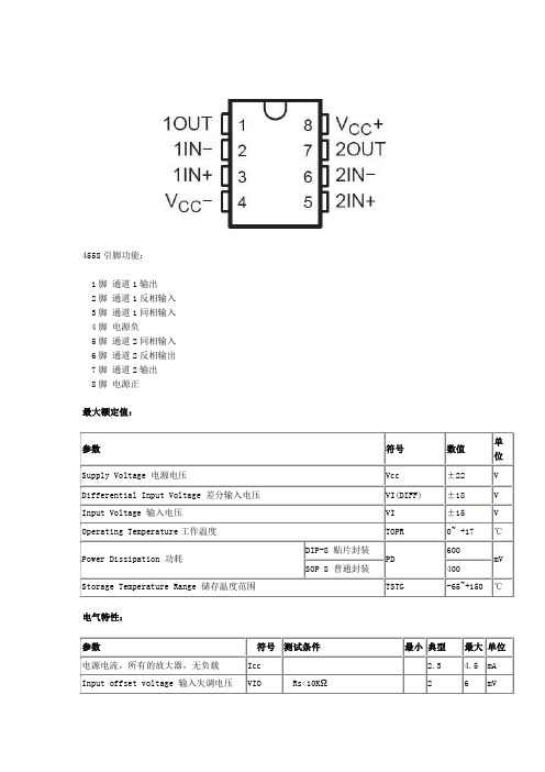
电气特性:
参数
符号
测试条件
最小
典型
最大
单位
电源电流,所有的放大器,无负载
Icc
2.3
4.5
mA
Input offset voltage输入失调电压
VIO
Rs<10KΩ
2
6
mV
Input offset current输入失调电流
IIO
5
200
nA
Input bias current输入偏置电流
IBIAS
参数符号测试条件最小典型最大单位电源电流所有的放大器无负载icc2345mainputoffsetvoltage输入失调电压viors10k?mvinputoffsetcurrent输入失调电流iio200nainputbiascurrent输入偏置电流ibias30500nalargesignalvoltagegain大信号电压增益gvvopp10vrl2k?20200vmvcommonmodeinputvoltagerange输入电压范围vir1213commonmoderejectionratio共模抑制cmrrrs10k?7090dbsupplyvoltagerejectionratio电源电压抑制比psrrrs10k?7690dboutputvoltageswing输出电压摆幅vopprl10k?1214powerconsumption功耗pc70170mvslewratesrvi10vrl2kcl100pf1222risetime上升时间trisvi20mvrl2kcl100pf03overshoot上过冲osvi20mvrl2kcl100pf15inputresistance输入电阻ri03outputresistance输出电阻ro75totalharmonicdistortion总谐波失真thdf1khzav20dbrl2kvo2vppcl100pf0008单位增益带宽bw28mhz
LG 微波炉 MG5018TR 使用说明书
联锁连续性测试 元件测试程序
故障检修 …………………………………………………………… (22) 立体解析图 (2 6) …………………………………………………………
部品清单 ………………………………………………………… (31)
2
安全措施
阅读此维修手册,使用正确的维修程序以确保持续的安全操作和采取措施来避免可能的微 波能源的辐射。
微波炉维修手册
注意: 在对本机检修之前,请先阅读本手册中“安全措施”
MG5018TR MG5018TW
目 录
(3) 安全措施 ………………………………………………………………… (4) 规格说明 ………………………………………………………………… (5) 注意事项 ………………………………………………………………… (6) 安装事宜 ………………………………………………………………… 操作指南 外观结构图/控制板图 ……………………………………………………… (7) 操作程序 …………………………………………………………… (8) 电路图 (9) ………………………………………………………………
A)不要打开炉门或在炉门开着时进行操作 B)在启动磁控管或其它产生微波的元件前对所有炉具进行下列安全检查, 并进行必要的修理 (1)联锁(2)门是否关得正确(3)密封垫和密封表面(弧光,磨损 或其它损坏(4)铰链和插销的损坏或松动(5)坠地或使用不当造成的 痕迹 C)在产生微波的分隔空间中接通微波电源进行任何维修测试或检验之前, 检查磁控管、波导管或波导线,以及炉体内各接线、插头是否正确的匹 配完整和连接 D)联锁监视器、门密封垫以及微波发射和传导系统的任何残次或安错的部 件,都在微波炉送给客户前按本手册规定的程序修理,替换或调节 E)微波炉售出前每一台微波炉都经过微波泄漏检测
453 维修手册
453 维修手册一、引言本维修手册是为453设备的用户和维修人员编写的,提供了设备日常维护、故障排除、高级维修技术等方面的指导和建议。
通过阅读本手册,您将能够更好地理解并操作453设备,同时掌握常见的维修技能和方法,以确保设备的正常运行和使用寿命。
二、设备概述453设备是一种高效、可靠的机械设备,广泛应用于各种工业领域。
本设备具有较高的精度和稳定性,能够满足各种生产需求。
为了更好地了解设备的结构和功能,请参阅设备附带的用户手册或相关技术文档。
三、维修工具与备件在进行维修时,您需要准备以下工具和备件:1. 螺丝刀:用于拆卸和安装设备的外壳和内部组件。
2. 扳手:用于固定和拆卸螺栓和螺母。
3. 润滑油:用于设备的润滑,保持设备运转顺畅。
4. 备件:根据设备的故障情况,可能需要更换的零部件,如轴承、密封圈等。
四、日常维护流程为了确保设备的正常运行和使用寿命,建议您按照以下日常维护流程进行操作:1. 定期检查设备的运行情况,如声音、温度、振动等,确保设备正常运转。
2. 定期清洁设备表面,保持设备整洁。
3. 检查设备的紧固件是否松动,如螺栓、螺母等,如有需要应及时固定。
4. 检查设备的润滑情况,定期加注润滑油,保持设备润滑良好。
5. 定期更换易损件,如密封圈、滤芯等,以保证设备的性能和使用寿命。
五、常见故障与排除在使用过程中,设备可能会出现各种故障。
以下是一些常见的故障与排除方法:1. 设备无法启动:检查电源是否正常,检查设备连接是否牢固。
如有问题,请及时沟通专业人员进行检查和维修。
2. 设备运行异常:可能是由于零部件损坏、润滑不足等原因引起的。
您可以检查设备的零部件是否损坏,同时加注润滑油,保持设备润滑良好。
如果问题无法解决,请及时沟通专业人员进行检查和维修。
3. 设备精度下降:可能是由于设备长时间使用或维护不当引起的。
您可以对设备进行校准和调整,以确保其精度。
如果问题无法解决,请及时沟通专业人员进行检查和维修。
Moxa ioThinx 4530 Series 高级模块控制器说明书
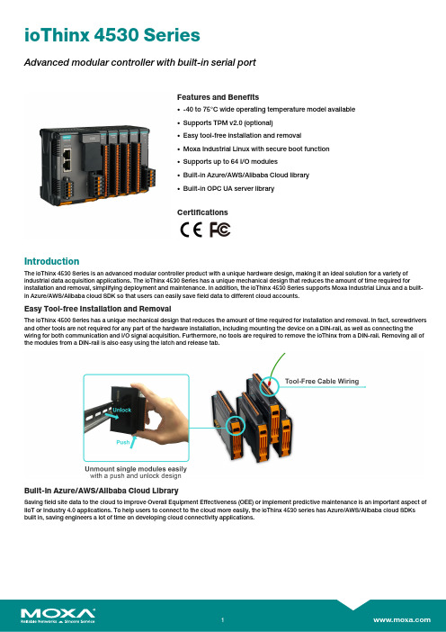
ioThinx4530SeriesAdvanced modular controller with built-in serial portFeatures and Benefits•-40to75°C wide operating temperature model available•Supports TPM v2.0(optional)•Easy tool-free installation and removal•Moxa Industrial Linux with secure boot function•Supports up to64I/O modules•Built-in Azure/AWS/Alibaba Cloud library•Built-in OPC UA server libraryCertificationsIntroductionThe ioThinx4530Series is an advanced modular controller product with a unique hardware design,making it an ideal solution for a variety of industrial data acquisition applications.The ioThinx4530Series has a unique mechanical design that reduces the amount of time required for installation and removal,simplifying deployment and maintenance.In addition,the ioThinx4530Series supports Moxa Industrial Linux and a built-in Azure/AWS/Alibaba cloud SDK so that users can easily save field data to different cloud accounts.Easy Tool-free Installation and RemovalThe ioThinx4500Series has a unique mechanical design that reduces the amount of time required for installation and removal.In fact,screwdrivers and other tools are not required for any part of the hardware installation,including mounting the device on a DIN-rail,as well as connecting the wiring for both communication and I/O signal acquisition.Furthermore,no tools are required to remove the ioThinx from a DIN-rail.Removing all of the modules from a DIN-rail is also easy using the latch and release tab.Built-in Azure/AWS/Alibaba Cloud LibrarySaving field site data to the cloud to improve Overall Equipment Effectiveness(OEE)or implement predictive maintenance is an important aspect of IIoT or Industry4.0applications.To help users to connect to the cloud more easily,the ioThinx4530series has Azure/AWS/Alibaba cloud SDKs built in,saving engineers a lot of time on developing cloud connectivity applications.SpecificationsComputerCPU NXP i.MX7D1GHzOS Linux kernel4.4(CIP,PREEMPT_RT),Debian9 Clock Real-time clock with capacitor backupDRAM512MB DDR3MRAM128kBStorage Pre-installed8GB eMMC(6GB reserved for the user) Storage Slot microSD Slots x1(up to32GB)Expansion Slots Up to64Control LogicLanguage C/C++,PythonComputer InterfaceButtons Reset buttonInput/Output InterfaceRotary Switch0to9Ethernet Interface10/100BaseT(X)Ports(RJ45connector)Auto negotiation speedMagnetic Isolation Protection 1.5kV(built-in)Serial InterfaceConsole Port RS-232(TxD,RxD,GND),3-pin(115200,n,8,1) No.of Ports1x RS-232/422or2x RS-485-2wConnector Spring-type Euroblock terminalSerial Standards RS-232/422/485(software selectable) Baudrate1200bps to115.2kbpsFlow Control RTS/CTSParity None,Even,OddStop Bits1,2Data Bits7,8Serial SignalsRS-232TxD,RxD,RTS,CTS,GNDRS-422Tx+,Tx-,Rx+,Rx-,GNDRS-485-2w Data+,Data-,GNDSystem Power ParametersPower Connector Spring-type Euroblock terminalNo.of Power Inputs1Input Voltage12to48VDCPower Consumption1940mA@12VDCOver-Current Protection3A@25°COver-Voltage Protection55VDCOutput Current1A(max.)Field Power ParametersPower Connector Spring-type Euroblock terminalNo.of Power Inputs1Input Voltage12/24VDCOver-Current Protection5A@25°COver-Voltage Protection33VDCOutput Current2A(max.)Physical CharacteristicsWiring Serial cable,16to28AWGPower cable,12to26AWGStrip Length Serial cable,9to10mmPower cable,12to13mmHousing PlasticDimensions60.3x99x75mm(2.37x3.9x2.96in)Weight207.7g(0.457lb)Installation DIN-rail mountingStandards and CertificationsEMC EN55032/24EMI CISPR32,FCC Part15B Class AEMS IEC61000-4-2ESD:Contact:4kV;Air:8kVIEC61000-4-3RS:80MHz to1000MHz:3V/mIEC61000-4-4EFT:Power:2kV;Signal:1kVIEC61000-4-5Surge:Power:2kV;Signal:1kVIEC61000-4-6CS:10VIEC61000-4-8PFMFShock IEC60068-2-27Vibration IEC60068-2-6MTBFStandards Telcordia SR332Time856,064hrsEnvironmental LimitsOperating Temperature ioThinx4533-LX:-20to60°C(-4to140°F)ioThinx4533-LX-T:-40to75°C(-40to167°F) Storage Temperature(package included)-40to85°C(-40to185°F)Ambient Relative Humidity5to95%(non-condensing)Altitude Up to4000mDeclarationGreen Product RoHS,CRoHS,WEEEWarrantyDetails See /warrantyWarranty Period5yearsPackage ContentsDevice1x ioThinx4530Series ControllerCable1x4-pin header to DB9console port Installation Kit1x terminal block,5-pin,5.00mm1x terminal block,5-pin,3.81mm Documentation1x warranty card1x quick installation guideDimensionsTop/Side/Bottom PanelsSide CoverOrdering InformationioThinx4533-LX C/C++,Python2x RJ45RS-232/RS-422/RS-48564-20to60°C ioThinx4533-LX-T C/C++,Python2x RJ45RS-232/RS-422/RS-48564-40to75°C Accessories(sold separately)I/O Modules45MR-1600Module for the ioThinx4500Series,16DIs,24VDC,PNP,-20to60°C operating temperature45MR-1600-T Module for the ioThinx4500Series,16DIs,24VDC,PNP,-40to75°C operating temperature45MR-1601Module for the ioThinx4500Series,16DIs,24VDC,NPN,-20to60°C operating temperature45MR-1601-T Module for the ioThinx4500Series,16DIs,24VDC,NPN,-40to75°C operating temperature45MR-2404Module for the ioThinx4500Series,4relays,form A,-20to60°C operating temperature45MR-2404-T Module for the ioThinx4500Series,4relays,form A,-40to75°C operating temperature45MR-2600Module for the ioThinx4500Series,16DOs,24VDC,sink,-20to60°C operating temperature45MR-2600-T Module for the ioThinx4500Series,16DOs,24VDC,sink,-40to75°C operating temperature45MR-2601Module for the ioThinx4500Series,16DOs,24VDC,source,-20to60°C operating temperature45MR-2601-T Module for the ioThinx4500Series,16DOs,24VDC,source,-40to75°C operating temperature45MR-2606Module for the ioThinx4500Series,8DIs,24VDC,PNP,8DOs,24VDC,source,-20to60°C operatingtemperature45MR-2606-T Module for the ioThinx4500Series,8DIs,24VDC,PNP,8DOs,24VDC,source,-40to75°C operatingtemperature45MR-3800Module for the ioThinx4500Series,8AIs,0to20mA or4to20mA,-20to60°C operating temperature 45MR-3800-T Module for the ioThinx4500Series,8AIs,0to20mA or4to20mA,-40to75°C operating temperature 45MR-3810Module for the ioThinx4500Series,8AIs,-10to10V or0to10V,-20to60°C operating temperature 45MR-3810-T Module for the ioThinx4500Series,8AIs,-10to10V or0to10V,-40to75°C operating temperature 45MR-4420Module for the ioThinx4500Series,4AOs,0to10V or0to20mA or4to20mA,-20to60°C operatingtemperature45MR-4420-T Module for the ioThinx4500Series,4AOs,0to10V or0to20mA or4to20mA,-40to75°C operatingtemperature45MR-6600Module for the ioThinx4500Series,6RTDs,-20to60°C operating temperature45MR-6600-T Module for the ioThinx4500Series,6RTDs,-40to75°C operating temperature45MR-6810Module for the ioThinx4500Series,8TCs,-20to60°C operating temperature45MR-6810-T Module for the ioThinx4500Series,8TCs,-40to75°C operating temperaturePower Modules45MR-7210Module for the ioThinx4500Series,system and field power inputs,-20to60°C operating temperature 45MR-7210-T Module for the ioThinx4500Series,system and field power inputs,-40to75°C operating temperature 45MR-7820Module for the ioThinx4500Series,potential distributor module,-20to60°C operating temperature 45MR-7820-T Module for the ioThinx4500Series,potential distributor module,-40to75°C operating temperature©Moxa Inc.All rights reserved.Updated Dec03,2019.This document and any portion thereof may not be reproduced or used in any manner whatsoever without the express written permission of Moxa Inc.Product specifications subject to change without notice.Visit our website for the most up-to-date product information.。
- 1、下载文档前请自行甄别文档内容的完整性,平台不提供额外的编辑、内容补充、找答案等附加服务。
- 2、"仅部分预览"的文档,不可在线预览部分如存在完整性等问题,可反馈申请退款(可完整预览的文档不适用该条件!)。
- 3、如文档侵犯您的权益,请联系客服反馈,我们会尽快为您处理(人工客服工作时间:9:00-18:30)。
1/10September 2001sRETRIGGERABLE/RESETTABLE CAPABILITY s TRIGGER AND RESET PROPAGATION DELAYS INDEPENDENT OF R X , C X s TRIGGERING FROM LEADING OR TRAILING EDGE s Q AND Q BUFFERED OUTPUT AVAILABLE s SEPARATE RESETS s WIDE RANGE OF OUTPUT PULSE WIDTHS s QUIESCENT CURRENT SPECIFIED UP TO 20V s 5V, 10V AND 15V PARAMETRIC RATINGS s SCHMITT TRIGGER INPUT ALLOWSUNLIMITED RISE AND FALL TIMES ON +TR AND -TR INPUTS s INPUT LEAKAGE CURRENTI I = 100nA (MAX) AT V DD = 18V T A = 25°C s 100% TESTED FOR QUIESCENT CURRENT s MEETS ALL REQUIREMENTS OF JEDEC JESD13B " STANDARD SPECIFICATIONS FOR DESCRIPTION OF B SERIES CMOS DEVICES"DESCRIPTIONThe HCF4538B is a monolithic integrated circuit fabricated in Metal Oxide Semiconductor technology available in DIP and SOP packages. The HCF4538B dual precision monostable multivibrator provides stable retriggerable/resettable one-shot operation for any fixed voltage timing application. An external resistor (R X ) and an external capacitor (C X ) control the timing and accuracy for the circuit. Adjustment of R X and C X provides a wide range of output pulse widths from the Q and Q terminals. The time delay from trigger input to output transition (trigger propagation delay) and the time delay from reset input to output transition (reset propagation delay) and the time delay from reset input to output transition (reset propagation delay) are independent of R X and C X . Precision control of output pulse width is achieved through linear CMOS techniques.Leading edge triggering (+TR) and trailing edge triggering (-TR) inputs are provided for triggeringHCF4538BDUAL MONOSTABLE MULTIVIBRATORPIN CONNECTIONORDER CODESPACKAGE TUBE T & R DIP HCF4538BEY SOPHCF4538BM1HCF4538M013TRHCF4538B2/10from either edge of an input pulse. An unused +TR input should be tied to V SS . An unused -TR input should be tied to V DD . A RESET (on low level) is provided for immediate termination of the output pulse or to prevent output pulses when power is turned on. An unused RESET input should be tied to V DD . However, if an entire section of the HCF4538B is not used, its inputs must be tied to either V DD or V SS (see table 1). In normal operation the circuit triggers (extends the output pulse one period) on the application of each new trigger pulse. For operation in the non-retiggerable mode, Q is connected to -TR when leading edge triggering (+TR) is used or Q is connected to +TR when trailing edge triggering (-TR) is used. The time period (T) for this multivibrator can be calculated by : T = R X C X . The min. value of external resistance, R X , is 4K Ω. The max. and min. values of external capacitance, C X , are 100µF and 5nF, respectively. IINPUT EQUIVALENT CIRCUITPIN DESCRIPTIONTerminals 1, 8, 15 are electrically connected internallyFUNCTIONAL DIAGRAMPIN No SYMBOL NAME AND FUNCTION 4, 12+TR Trigger Inputs (Low to High, Edge-Triggered)5, 11-TR Trigger Inputs (High to Low, Edge-Triggered)3, 13RESET Direct Reset Inputs (Active Low)1, 15C X 1, C X 2External Capacitor Con-nections2, 14R X C X 1R X C X 2External Resistor/Capaci-tor Connections 6, 10Q1, Q2Pulse Outputs7, 9Q1, Q2Complementary Pulse Outputs8V SS Negative Supply Voltage 16V DDPositive Supply VoltageHCF4538B3/10TABLE 1 : Functional Terminal ConnectionsA Retriggerable one-shot multivibrator has an output pulse width which is extended on full time period (T) after application of the last trigger pulse.A Non-Retriggerable one-shot multivibrator has a time period (T) referenced from the application of the firs trigger pulse.LOGIC DIAGRAMFUNCTIONV DD to Term. N °V SS to Term. N °Input Pulse to Term. N °Other ConnectionsMono (1)Mono (2)Mono (1)Mono (2)Mono (1)Mono (2)Mono (1)Mono (2)Leading Edge Trigger/Retriggerable3, 511, 13412Leading Edge Trigger/NonRetriggerable 3134125, 711, 9Trailing Edge Trigger/Retriggerable313412511Trailing Edge Trigger/NonRetriggerable3135114, 612, 10HCF4538B4/10LOGIC DIAGRAMABSOLUTE MAXIMUM RATINGSAbsolute Maximum Ratings are those values beyond which damage to the device may occur. Functional operation under these conditions is not implied.All voltage values are referred to V SS pin voltage.RECOMMENDED OPERATING CONDITIONSSymbol ParameterValue Unit V DD Supply Voltage-0.5 to +22V V I DC Input Voltage -0.5 to V DD + 0.5V I I DC Input Current± 10mA P D Power Dissipation per Package200mW Power Dissipation per Output Transistor 100mW T op Operating Temperature -55 to +125°C T stgStorage Temperature-65 to +150°CSymbol ParameterValue Unit V DD Supply Voltage 3 to 20V V I Input Voltage0 to V DD V T opOperating Temperature-55 to 125°CHCF4538B5/10DC SPECIFICATIONSThe Noise Margin for both "1" and "0" level is: 1V min. with V DD =5V, 2V min. with V DD =10V, 2.5V min. with V DD =15VSymbolParameterTest ConditionValue UnitV I (V)V O (V)|I O |(µA)V DD (V)T A = 25°C -40 to 85°C -55 to 125°C Min.Typ.Max.Min.Max.Min.Max.I LQuiescent Current0/550.045150150µA0/10100.0410*******/15150.04206006000/20200.0810030003000V OHHigh Level Output Voltage0/5<15 4.95 4.95 4.95V0/10<1109.959.959.950/15<11514.9514.9514.95V OLLow Level Output Voltage5/0<150.050.050.05V10/0<1100.050.050.0515/0<1150.050.050.05V IHHigh Level Input Voltage 0.5/4.5<15 3.5 3.5 3.5V1/9<1107771.5/13.5<115111111V ILLow Level Input Voltage 4.5/0.5<15 1.5 1.5 1.5V9/1<11033313.5/1.5<115444I OHOutput Drive Current0/5 2.5<15-1.6-3.2-1.3-1.3mA0/5 4.6<15-0.51-1-0.42-0.420/109.5<110-1.3-2.6-1.1-1.10/1513.5<115-3.4-6.8-2.8-2.8I OLOutput Sink Current0/50.4<15-0.511-0.42-0.42mA 0/100.5<110-1.3 2.6-1.1-1.10/15 1.5<115-3.46.8-2.8-2.8I I Input Leakage Current0/18Any Input 18±10-5±0.1±1±1µA C IInput CapacitanceAny Input57.5pFHCF4538B6/10DYNAMIC ELECTRICAL CHARACTERISTICS (T amb = 25°C, C L = 50pF, R L = 200K Ω, t r = t f = 20 ns)(*) Typical temperature coefficient for all V DD value is 0.3 %/°C.(1) Minimum R X value = 4K Ω , minimum C X value = 5000 pFSymbolParameterTest ConditionValue (*)UnitV DD (V)Min.Typ.Max.t TLH t THL Transition Time5100200ns 1050100154080t PLH t PHL Propagation Delay Time+TR or -TR to Q or Q 5300600ns1015030015100200t PLH t PHL Propagation Delay TimeReset to Q or Q 5R L = 1K Ω250500ns101252501595190t WH t WLMinimum Input Pulse Width +TR, -TR or Reset 5R L = 1K Ω80140ns104080153060t WTOutput Pulse Width - Q or Q (C X = 0.005 µF, R X = 10K Ω (1))55760.664.5µs105558.963.0155559.163.5t WTOutput Pulse Width - Q or Q (C X = 0.1µF, R X = 100K Ω)59.49.9710.5ms109.49.9510.6159.510.010.6t WTOutput Pulse Width - Q or Q (C X = 10µF, R X = 100K Ω)50.95 1.0 1.06s100.95 1.0 1.06150.961.0 1.07t WPulse Width MatchBetween Circuits in Same Package : (100(T 1 - T 2)/T 1) (C X = 0.1µF, R X = 100K Ω) 5± 1%10± 115± 1t rrMinimum Retrigger Time50ns 100150C INInput CapacitanceAny Input57.5pFHCF4538B7/10TEST CIRCUITLR L = 200K ΩR T = Z OUT of pulse generator (typically 50Ω)WAVEFORM : PROPAGATION DELAY TIMES (f=1MHz; 50% duty cycle)HCF4538BInformation furnished is believed to be accurate and reliable. However, STMicroelectronics assumes no responsibility for the consequences of use of such information nor for any infringement of patents or other rights of third parties which may result from its use. No license is granted by implication or otherwise under any patent or patent rights of STMicroelectronics. Specifications mentioned in this publication are subject to change without notice. This publication supersedes and replaces all information previously supplied. STMicroelectronics products are not authorized for use as critical components in life support devices or systems without express written approval of STMicroelectronics.© The ST logo is a registered trademark of STMicroelectronics© 2001 STMicroelectronics - Printed in Italy - All Rights ReservedSTMicroelectronics GROUP OF COMPANIESAustralia - Brazil - China - Finland - France - Germany - Hong Kong - India - Italy - Japan - Malaysia - Malta - MoroccoSingapore - Spain - Sweden - Switzerland - United Kingdom© 10/10。