MBR20080CT中文资料
MBR10200CT-MBR20100CT ASEMI高压肖特基二极管规格
MBR10200CT ASEMI高压肖特基二极管
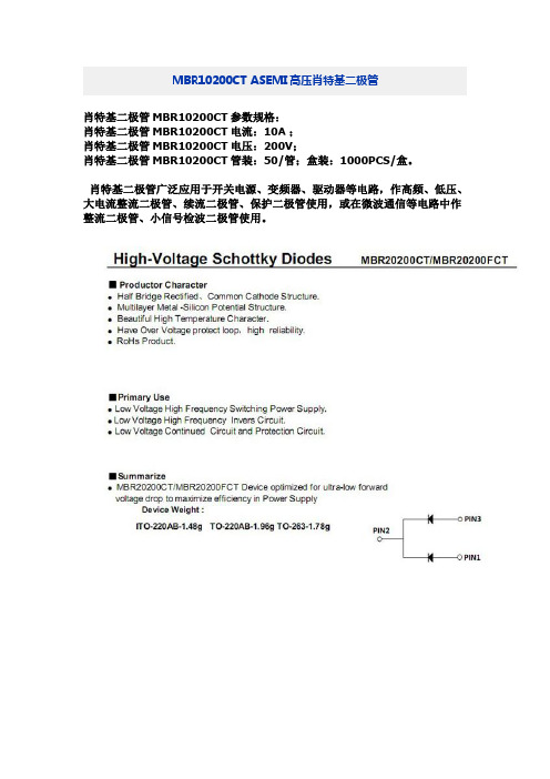
肖特基二极管MBR10200CT参数规格:
肖特基二极管MBR10200CT电流:10A;
肖特基二极管MBR10200CT电压:200V;
肖特基二极管MBR10200CT管装:50/管;盒装:1000PCS/盒。
肖特基二极管广泛应用于开关电源、变频器、驱动器等电路,作高频、低压、大电流整流二极管、续流二极管、保护二极管使用,或在微波通信等电路中作整流二极管、小信号检波二极管使用。
MBR10200CT ITO-220AB肖特基二极管PDF资料
MBR10200CT肖特基类型:高结温芯片,品牌:ASEMI,
应用市场:电源,小家电,LED电源,各式充电器,开关电源,LED显示屏等。
MBR10200CT肖特基相关参数如下:
MBR10200CT电压Vrrm:200V
MBR10200CT电流If平均:10A
MBR10200CT正向电压Vf最大:0.87V
MBR10200CT电流,Ifs最大:150A
MBR10200CT工作温度范围:-40°C to+150°C
MBR10200CT封装形式:TO-220/TO-220F/ITO-220
MBR10200CT反向恢复电流,Irrm:10UA
肖特基系列型号:
MBR1040CT,MBR1045CT,MBR1060CT,MBR1060FCT, MBR10100CT,MBR10100FCT,MBR10150FCT,MBR10150CT, MBR10200FCT,MBR10200CT
肖特基二极管封装:TO-251,TO-252,TO-263,
TO-220,TO-247,TO-3P。
MBRF20H150CT中文资料

Features• Plastic package has Underwriters Laboratory Flammability Classification 94V-0• Dual rectifier construction, positive center tap • Metal silicon junction, majority carrier conductionPlated leads, solderable per As marked Mounting Position: Any 10 in-lbs maximum MBR20H150CT , MBRF20H150CT & MBRB20H150CT-1 SeriesVishay Semiconductorsformerly General SemiconductorDocument Number New ProductReverse Voltage 150V Forward Current 20AMax. Junction Temperature 175°CPIN 1PIN 3TO-220AB (MBR20H150CT)TO-262AA (MBRB20H150CT-1)Maximum Ratings (TC= 25°C unless otherwise noted)ParameterSymbol MBR20H150CTUnit Maximum repetitive peak reverse voltage V RRM 150V Working peak reverse voltage V RWM 150V Maximum DC blocking voltageV DC150V Maximum average forward rectified current Total device20Per legI F(AV)10A Peak forward surge current8.3ms single half sine-wave superimposed I FSM 200A on rated load (JEDEC Method) per legPeak repetitive reverse current per leg at t p = 2µs, 1KH Z I RRM 1.0A Peak non-repetitive reverse surge energy per leg E RSM 10mJ (8/20µs waveform)Non-repetitive avalanche energy per leg at 25°C, I AS = 1.5A, L=10mH E AS 11.25mJ Voltage rate of change (rated V R )dv/dt 10,000V/µs Operating junction and storage temperature range T J , T STG –65 to +175°C RMS Isolation voltage (MBRF type only) from terminals 4500(1)to heatsink with t = 1 second, RH ≤30%V ISOL3500(2)V1500 (3)Electrical Characteristics (TC= 25°C unless otherwise noted)ParameterSymbolValue UnitMaximum instantaneous I F = 10A,T C = 25°C 0.90forward voltage per leg at (4):I F = 10A,T C = 125°C 0.75I F = 20A,T C = 25°C V F 0.99V I F = 20A,T C = 125°C 0.86Maximum reverse current per leg T J = 25°C 5.0µA at working peak reverse voltageT J = 125°CI R1.0mAThermal Characteristics (TC= 25°C unless otherwise noted)ParameterSymbol MBR MBRF MBRB Unit Typical thermal resistance per legR ΘJC2.24.22.2°C/WNotes:(1) Clip mounting (on case), where lead does not overlap heatsink with 0.110” offset (2) Clip mounting (on case), where leads do overlap heatsink(3) Screw mounting with 4-40 screw, where washer diameter is ≤ 4.9 mm (0.19”)(4) Pulse test: 300µs pulse width, 1% duty cycleMBR20H150CT , MBRF20H150CT & MBRB20H150CT-1 SeriesVishay Semiconductorsformerly General Semiconductor Document Number 88864MBR20H150CT , MBRF20H150CT & MBRB20H150CT-1 SeriesVishay Semiconductorsformerly General SemiconductorDocument Number 0.10.30.20.40.60.8 1.00.50.70.9 1.1 1.2100100.110.10.011101001,00010,0000.01110010101000.10.11Fig. 3 – Typical Instantaneous Forward Characteristics Per LegI R -- I n s t a n t a n e o u s R e v e r s e C u r r e n t (µA )J u n c t i o n C a p a c i t a n c e (p F )1101001001000100000.110Reverse Voltage (V)102030507010040608090Fig. 4 – Typical Reverse Characteristics Per LegFig. 6 – Typical Transient Thermal Impedance Per Legt -- Pulse Duration (sec.)Instantaneous Forward Voltage (V)Percent of Rated Peak Reverse Voltage (%)I F -- I n s t a n t a n e o u s F o r w a r d C u r r e n t (A )T r a n s i e n t T h e r m a l I m p e d a n c e (°C /W )51015202530255075100125150175A v e r a g e F o r w a r d C u r r e n t (A )Case T emperature (°C)020406080100120140160180200220240200110100P e a k F o r w a r d S u r g e C u r r e n t (A )Number of Cycles at 60 H ZFig. 5 – Typical Junction CapacitancePer LegFig. 1 – Forward Derating Curve(Total)Fig. 2 – Maximum Non-Repetitive Peak Forward Surge Current Per LegRatings andCharacteristic Curves (T A = 25°C unless otherwise noted)This datasheet has been download from: Datasheets for electronics components.。
MBRFL20200CT Rev.A Sep.-2022 数据表说明书
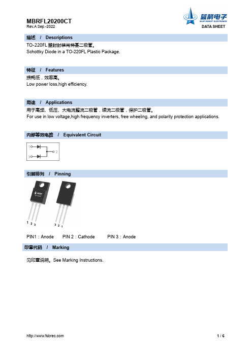
TO-220FL 塑封封装肖特基二极管。
Schottky Diode in a TO-220FL Plastic Package.损耗低,效率高。
Low power loss,high efficiency.用于高频、低压、大电流整流二极管,续流二极管,保护二极管。
For use in low voltage,high frequency inverters, free wheeling, and polarity protection applications.PIN1:Anode PIN 2:Cathode PIN 3:Anode印章代码 / Marking见印章说明。
See Marking Instructions .描述 / Descriptions特征 / Features 用途 / Applications内部等效电路 / Equivalent Circuit引脚排列 / Pinning参数Parameter符号 Symbol 数值 Rating单位 UnitPeak Repetitive Reverse Voltage V RRM 200 V Working Peak Reverse Voltage V RWM200 VPeak Repetitive Forward Current I FRM 20 A Average Rectified Forward Current I F(AV) 10 A I F(AV)(total )20 A Non Repetitive Peak Surge Current I FSM 150 A Peak Repetitive Reverse Current I RRM 1.0 AThermal Resistance Junction to Case R θJc 2.0 /W ℃Junction Temperature Range T j 150 ℃ Storage Temperature RangeT stg-65~150℃参数Parameter符号 Symbol测试条件 Test Conditions最小值 Min 典型值 Typ 最大值 Max单位UnitForward VoltageV FI F =10A(T j =25)℃ 0.9 VI F =10A(T j =125)℃ 0.8 V I F =20A(T j =25)℃ 1.0 V I F =20A(T j =125)℃ 0.9 VInstantaneous Reverse Current I R V R =200V(T j =25)℃ 1.0 mA V R =200V(T j =125)℃ 50 mA Voltage Rate of Changedv/dt10000V/μs极限参数 / Absolute Maximum Ratings(Ta=25℃) 电性能参数 / Electrical Characteristics(Ta=25℃)电参数曲线图 / Electrical Characteristic Curve外形尺寸图 / Package Dimensions印章说明 / Marking Instructions说明: BR: 为公司代码 MBRL20200: 为产品型号CT: 为内部结构****:为生产批号代码,随生产批号变化Note:BR: Company Code MBRL20200:Product TypeCT: Internal Structure ****:Lot No. Code, code change with Lot NoBR****MBRL20200CT波峰焊温度曲线图(无铅) / Temperature Profile for Dip Soldering(Pb-Free)说明:Note:1、预热温度25~150℃,时间60~90sec; 1.Preheating:25~150℃, Time:60~90sec.2、峰值温度255±5℃,时间持续为5±0.5sec; 2.Peak Temp.:255±5℃, Duration:5±0.5sec.3、焊接制程冷却速度为2~10℃/sec. 3. Cooling Speed: 2~10℃/sec.耐焊接热试验条件 / Resistance to Soldering Heat Test Conditions 温度:270±5℃ 时间:10±1 sec. Temp.:270±5℃ Time:10±1 sec包装规格 / Packaging SPEC. 套管包装 / TUBEPackage Type封装形式Units 包装数量 Dimension 包装尺寸 (unit :mm 3)Units/Tube只/套管Tubes/Inner Box 套管/盒Units/Inner Box只/盒Inner Boxes/Outer Box 盒/箱 Units/Outer Box只/箱Tube 套管 Inner Box 盒 Outer Box 箱TO-220FL 50 20 1,000 55,000 532×33×7.0 555×164×50575×290×180使用说明 / Notices。
MBRS10100CT资料
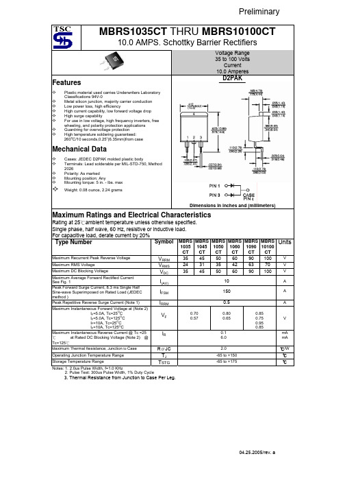
100
0.70 0.57 0.80 0.65 0.1 6.0 2.0 -65 to +150 -65 to +175 0.85 0.75 0.95 0.85
V mA mA ℃/W ℃ ℃
TSTG
TJ
3. Thermal Resistance from Junction to Case Per Leg.
04.25.2005/rev. a
元器件交易网
RATINGS AND CHARACTERISTIC CURVES (MBRS1035CT THRU MBRS10100CT)
FIG.1- FORWARD CURRENT DERATING CURVE
5.0
180
FIG.2- MAXIMUM NON-REPETITIVE FORWARD SURGE CURRENT PER LEG
Plastic material used carries Underwriters Laboratory Classifications 94V-0 Metal silicon junction, majority carrier conduction Low power loss, high efficiency High current capability, low forward voltage drop High surge capability For use in low voltage, high frequency inverters, free wheeling, and polarity protection applications Guardring for overvoltage protection High temperature soldering guaranteed: 260oC/10 seconds,0.25”(6.35mm)from case
MBR20H100CT中文资料

MBR20H100CT , MBRF20H100CT & MBRB20H100CT SeriesVishay Semiconductorsformerly General SemiconductorDocument Number New ProductCase:JEDEC TO-220AB, ITO-220AB, TO-263AB & TO-262AA molded plastic bodyTerminals:Plated leads, solderable per MIL-STD-750, Method 2026High temperature soldering guaranteed:250°C/10 seconds, 0.25" (6.35mm) from case (TO-220AB,ITO-220AB & TO-252AA) at terminals (TO-236AB)Polarity:As marked Mounting Position: Any Mounting Torque:10 in-lbs maximum Weight:0.08 oz., 2.24 g• Plastic package has Underwriters Laboratory Flammability Classification 94V-0• Dual rectifier construction, positive center tap • Metal silicon junction, majority carrier conduction • Low power loss, high efficiency• Guardring for overvoltage protection• For use in low voltage, high frequency inverters, free wheeling, and polarity protection applicationsMBR20H100CT , MBRF20H100CT & MBRB20H100CT SeriesVishay Semiconductorsformerly General Semiconductor Document Number 88673Maximum Ratings (TC= 25°C unless otherwise noted)ParameterSymbol MBR20H90CTMBR20H100CTUnit Maximum repetitive peak reverse voltage V RRM 90100V Working peak reverse voltage V RWM 90100V Maximum DC blocking voltageV DC90100V Maximum average forward rectified current Total device20Per legI F(AV)10A Peak forward surge current8.3ms single half sine-wave superimposed I FSM 250A on rated load (JEDEC Method) per legPeak repetitive reverse current per leg at t p = 2µs, 1KH Z I RRM 1.0A Voltage rate of change (rated V R )dv/dt 10,000V/µs Operating junction and storage temperature range T J , T STG –65 to +175°C RMS Isolation voltage (MBRF type only) from terminals 4500(1)to heatsink with t = 1 second, RH ≤30%V ISOL3500(2)V1500 (3)Electrical Characteristics (TC= 25°C unless otherwise noted)ParameterSymbolValue UnitMaximum instantaneous I F = 10A,T C = 25°C 0.77forward voltage per leg at (4):I F = 10A,T C = 125°C 0.64I F = 20A,T C = 25°C V F 0.88V I F = 20A,T C = 125°C 0.73Maximum reverse current per leg T J = 25°C 4.5µA at working peak reverse voltageT J = 125°CI R6.0mAThermal Characteristics (TC= 25°C unless otherwise noted)ParameterSymbol MBR MBRF MBRB Unit Typical thermal resistance per legR ΘJC2.05.82.0°C/WNotes:(1) Clip mounting (on case), where lead does not overlap heatsink with 0.110” offset (2) Clip mounting (on case), where leads do overlap heatsink(3) Screw mounting with 4-40 screw, where washer diameter is ≤ 4.9 mm (0.19”)(4) Pulse test: 300µs pulse width, 1% duty cycleOrdering InformationProductCase Package CodePackage OptionMBR20H90CT - MBR20H100CT TO-220AB 45Anti-Static tube, 50/tube, 2K/carton MBRF20H90CT - MBRF20H100CT ITO-220AB 45Anti-Static tube, 50/tube, 2K/carton 3113” reel, 800/reel, 4.8K/cartonMBRB20H90CT - MBRB20H100CTTO-263AB45Anti-Static tube, 50/tube, 2K/carton81Anti-Static 13” reel, 800/reel, 4.8K/cartonMBR20H100CT , MBRF20H100CT & MBRB20H100CT SeriesVishay Semiconductorsformerly General SemiconductorDocument Number Ratings andCharacteristic Curves per leg (TA= 25°C unless otherwise noted)481220160.11101001000Fig. 1 — Forward Current Derating CurveFig. 2 — Maximum Non-Repetitive PeakForward Surge Current Per Leg0.010.1110。
MBRB20200CT中文资料
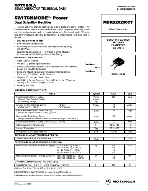
ELECTRICAL CHARACTERISTICS (PER LEG)
Maximum Instantaneous Forward Voltage (1) 0.9 0.8 1.0 0.9 1.0 50 Volts
Maximum Instantaneous Reverse Current (1) (Rated dc Voltage, TC = 25°C) (Rated dc Voltage, TC = 125°C)
Amps Amps Amps Amp °C °C V/µs °C/W
THERMAL CHARACTERISTICS (PER LEG)
Thermal Resistance — Junction to Case RθJC (IF = 10 Amps, TC = 25°C) (IF = 10 Amps, TC = 125°C) (IF = 20 Amps, TC = 25°C) (IF = 20 Amps, TC = 125°C) VF 2.0
150
160
Figure 3. Forward Power Dissipation
IF(AV), AVERAGE FORWARD CURRENT (AMPS) 20 500
Figure 4. Current Derating, Case
RθJA = 16°C/W RATED VOLTAGE C, CAPACITANCE (pF)
Figure 2. Typical Reverse Current (Per Leg)
SQUARE WAVE
RATED VOLTAGE RθJC = 2°C/W
20
15 SQUARE WAVE 10 dc
5
0
90
MBR2080CTG;MBR2090CTG;MBR20100CT;MBR2090CT;MBR20100CTG;中文规格书,Datasheet资料

MBR2080CT, MBR2090CT, MBR20100CT SWITCHMODE™Power RectifiersThis series uses the Schottky Barrier principle with a platinum barrier metal. These state−of−the−art devices have the following features:Features•20 A Total (10 A Per Diode Leg)•Guard−Ring for Stress Protection•Low Forward V oltage•175°C Operating Junction Temperature•Epoxy Meets UL 94 V−0 @ 0.125 in•Low Power Loss/High Efficiency•High Surge Capacity•Low Stored Charge Majority Carrier Conduction •Shipped 50 units per plastic tube•Pb−Free Packages are Available*Mechanical Characteristics:•Case: Epoxy, Molded•Weight: 1.9 grams (approximately)•Finish: All External Surfaces Corrosion Resistant and Terminal Leads are Readily Solderable•Lead Temperature for Soldering Purposes:260°C Max. for 10 Seconds*For additional information on our Pb−Free strategy and soldering details, please download the ON Semiconductor Soldering and Mounting Techniques Reference Manual, SOLDERRM/D.TO−220ABCASE 221APLASTICSCHOTTKY BARRIERRECTIFIERS20 AMPERES80−100 VOLTS132, 4MARKING DIAGRAMA= Assembly LocationY= YearWW= Work WeekB20x0= Device Codex= 8, 9 or 10G= Pb−Free DeviceAKA= Polarity DesignatorSee detailed ordering and shipping information in the package dimensions section on page 2 of this data sheet.ORDERING INFORMATIONMAXIMUM RATINGS (Per Diode Leg)Rating SymbolMBRUnit 2080CT2090CT20100CTPeak Repetitive Reverse Voltage Working Peak Reverse Voltage DC Blocking Voltage V RRMV RWMV R8090100VAverage Rectified Forward Current(Rated V R) T C = 133°CI F(AV)10APeak Repetitive Forward Current(Rated V R, Square Wave, 20 kHz) T C = 133°CI FRM20ANonrepetitive Peak Surge Current(Surge applied at rated load conditions halfwave,single phase, 60 Hz)I FSM150APeak Repetitive Reverse Surge Current (2.0 m s, 1.0 kHz)I RRM0.5A Operating Junction Temperature (Note 1)T J*65 to +175°C Storage Temperature T stg*65 to +175°C Voltage Rate of Change (Rated V R)dv/dt10,000V/m s THERMAL CHARACTERISTICSMaximum Thermal Resistance Junction−to−CaseJunction−to−Ambient R q JCR q JA2.060°C/WELECTRICAL CHARACTERISTICS (Per Diode Leg)Maximum Instantaneous Forward Voltage (Note 2) (i F = 10 Amps, T C = 125°C)(i F = 10 Amps, T C = 25°C)(i F = 20 Amps, T C = 125°C)(i F = 20 Amps, T C = 25°C)v F0.750.850.850.95VMaximum Instantaneous Reverse Current (Note 2) (Rated dc Voltage, T C = 125°C)(Rated dc Voltage, T C = 25°C)i R6.00.1mA1.The heat generated must be less than the thermal conductivity from Junction−to−Ambient: dP D/dT J < 1/R q JA.2.Pulse Test: Pulse Width = 300 m s, Duty Cycle ≤2.0%.ORDERING INFORMATIONDevice Package Shipping†MBR2080CT TO−22050 Units / RailMBR2080CTG TO−220(Pb−Free)MBR2090CT TO−22050 Units / RailMBR2090CTG TO−220(Pb−Free)MBR20100CT TO−22050 Units / RailMBR20100CTG TO−220(Pb−Free)†For information on tape and reel specifications, including part orientation and tape sizes, please refer to our Tape and Reel Packaging Specifications Brochure, BRD8011/D.Figure 1. Typical Forward Voltage Per Diode Figure 2. Typical Reverse Current Per DiodeFigure 3. Typical Current Derating, Case, Per Leg Figure 4. Typical Current Derating, Ambient, Per LegFigure 5. Average Power Dissipation andAverage Current0.6v F , INSTANTANEOUS VOLTAGE (VOLTS)205010V R , REVERSE VOLTAGE (VOLTS)T C, CASE TEMPERATURE (°C)15T A , AMBIENT TEMPERATURE (°C)204.08.0AVERAGE CURRENT (AMPS)208.06.04.02.00 6.0i F , I N S T A N T A N E O U S F O R W A R D C U R R E N T (A M P S )I I I F (A V ), A V E R A G E F O R W A R D C U R R E N T (A M P S )5.03.00.20.40.8204060800.11.0102012141.00.51.0, R E V E R S E C U R R E N T (m A )R 10, A V E R A G E F O R W A R D C U R R E N T (A M P S )F (A V ) 2.014161810120.0110201510A V E R A G E P O W E R (W A T T S )0.50.10.30.70.91005.0 5.018160.00010.001PACKAGE DIMENSIONSTO −220CASE 221A −09ISSUE AFNOTES:1.DIMENSIONING AND TOLERANCING PER ANSI Y14.5M, 1982.2.CONTROLLING DIMENSION: INCH.3.DIMENSION Z DEFINES A ZONE WHERE ALL BODY AND LEAD IRREGULARITIES ARE ALLOWED.STYLE 6:PIN 1.ANODE 2.CATHODE 3.ANODE 4.CATHODEDIM MIN MAX MIN MAX MILLIMETERS INCHES A 0.5700.62014.4815.75B 0.3800.4059.6610.28C 0.1600.190 4.07 4.82D 0.0250.0350.640.88F 0.1420.161 3.61 4.09G 0.0950.105 2.42 2.66H 0.1100.155 2.80 3.93J 0.0140.0250.360.64K 0.5000.56212.7014.27L 0.0450.060 1.15 1.52N 0.1900.210 4.83 5.33Q 0.1000.120 2.54 3.04R 0.0800.110 2.04 2.79S 0.0450.055 1.15 1.39T 0.2350.255 5.97 6.47U 0.0000.0500.00 1.27V 0.045--- 1.15---Z---0.080--- 2.04FSEATINGPLANEON Semiconductor and are registered trademarks of Semiconductor Components Industries, LLC (SCILLC). SCILLC reserves the right to make changes without further notice to any products herein. SCILLC makes no warranty, representation or guarantee regarding the suitability of its products for any particular purpose, nor does SCILLC assume any liability arising out of the application or use of any product or circuit, and specifically disclaims any and all liability, including without limitation special, consequential or incidental damages.“Typical” parameters which may be provided in SCILLC data sheets and/or specifications can and do vary in different applications and actual performance may vary over time. All operating parameters, including “Typicals” must be validated for each customer application by customer’s technical experts. SCILLC does not convey any license under its patent rights nor the rights of others. SCILLC products are not designed, intended, or authorized for use as components in systems intended for surgical implant into the body, or other applications intended to support or sustain life, or for any other application in which the failure of the SCILLC product could create a situation where personal injury or death may occur. Should Buyer purchase or use SCILLC products for any such unintended or unauthorized application, Buyer shall indemnify and hold SCILLC and its officers, employees, subsidiaries, affiliates,and distributors harmless against all claims, costs, damages, and expenses, and reasonable attorney fees arising out of, directly or indirectly, any claim of personal injury or death associated with such unintended or unauthorized use, even if such claim alleges that SCILLC was negligent regarding the design or manufacture of the part. SCILLC is an Equal Opportunity/Affirmative Action Employer. This literature is subject to all applicable copyright laws and is not for resale in any manner.PUBLICATION ORDERING INFORMATIONSWITCHMODE is a trademark of Semiconductor Components Industries, LLC (SCILLC).分销商库存信息:ONSEMIMBR2080CTG MBR2090CTG MBR20100CT MBR2090CT MBR20100CTG MBR2090CTLFAJG MBR2080CT。
MBR20150中文资料
IR(µA) 1E+5
1E+4
1E+3
1E+2
1E+1
1E+0
1E-1
0
25
Tj=175°C Tj=150°C Tj=125°C
Tj=100°C
C(pF) 1000
100
Tj=25°C
VR(V)
50
75 100 125 150
10 12
F=1MHz Tj=25°C
VR(V) 5 10 20
50 100 200
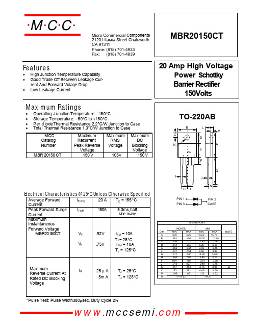
rent And Forward Volage Drop • Low Leakage Current
MBR20150CT
20 Amp High Voltage Power Schottky Barrier Rectifier 150Volts
Maximum Ratings
• Operating J unction Temperature : 150°C • Storage Temperature: - 50°C to +150°C • Per d iode Thermal Resistance 2.2°C/W Junction to Case • Total Thermal Resistance 1.3°C/W Junction to Case
IFM = 10A
TJ = 25°C
VF
.75V
I FM = 10A
TJ = 125°C
Maximum Reverse Current At
IR
Rated DC Blocking
Voltage
25 µ A 5m A
TJ = 25°C TJ = 125°C
MBRF20200CT中文资料
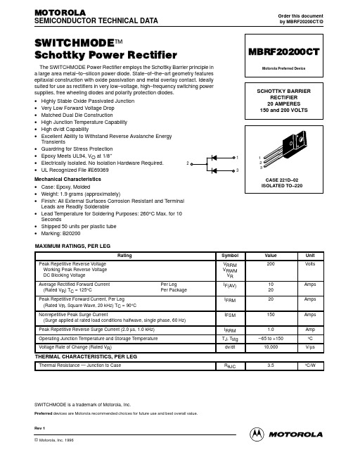
1
元器件交易网 MBRF20200CT
ELECTRICAL CHARACTERISTICS, PER LEG
Rating Maximum Instantaneous Forward Voltage (1) (iF = 10 Amp, TC = 25°C) (iF = 10 Amp, TC = 125°C) (iF = 20 Amp, TC = 25°C) (iF = 20 Amp, TC = 125°C) Maximum Instantaneous Reverse Current (1) (Rated dc Voltage, TC = 25°C) (Rated dc Voltage, TC = 125°C) Symbol vF 0.9 0.8 1.0 0.9 iR 1.0 50 mA Max Unit Volts
MBRP30060CT资料

Max 45 60 300 150 300 2500 2.0
Unit Volts
Amps Amps Amps Amps °C °C V/µs
*55 to +175 *55 to +150
10000 0.45
THERMAL CHARACTERISTICS PER LEG
Thermal Resistance, Junction to Case RθJC °C/W
©RectifierInc. 1996 Data Motorola, Device
1
元器件交易网 MBRP30045CT MBRP30060CT
PACKAGE DIMENSIONS
–A– R G –B–
W 0.25 (0.010) N
M
T A
M
B
M
NOTES: 1. DIMENSIONING AND TOLERANCING PER ANSI Y14.5M, 1982. 2. CONTROLLING DIMENSION: INCH. 3. TERMINAL PENETRATION: 5.97 (0.235) MAXIMUM. INCHES MIN MAX 3.450 3.635 0.700 0.810 0.615 0.640 0.120 0.130 0.435 0.445 1.370 1.380 0.007 0.030 1/4–20UNC–2B 0.270 0.285 31.50 BSC 0.600 0.630 0.330 0.375 0.170 0.190 MILLIMETERS MIN MAX 87.63 92.33 17.78 20.57 15.53 16.26 3.05 3.30 11.05 11.30 34.80 35.05 0.18 0.76 1/4–20UNC–2B 6.86 7.32 80.01 BSC 15.24 16.00 8.39 9.52 4.32 4.82
MBRB20100CTG中文资料
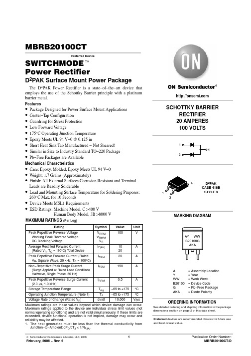
MBRB20100CTPreferred Device SWITCHMODE tPower RectifierD2PAK Surface Mount Power PackageThe D2PAK Power Rectifier is a state−of−the−art device that employs the use of the Schottky Barrier principle with a platinum barrier metal.Features•Package Designed for Power Surface Mount Applications •Center−T ap Configuration•Guardring for Stress Protection•Low Forward V oltage•175°C Operating Junction Temperature•Epoxy Meets UL 94 V−0 @ 0.125 in•Short Heat Sink Tab Manufactured − Not Sheared!•Similar in Size to Industry Standard TO−220 Package•Pb−Free Packages are AvailableMechanical Characteristics•Case: Epoxy, Molded, Epoxy Meets UL 94 V−0•Weight: 1.7 Grams (Approximately)•Finish: All External Surfaces Corrosion Resistant and Terminal Leads are Readily Solderable•Lead and Mounting Surface Temperature for Soldering Purposes: 260°C Max. for 10 Seconds•Device Meets MSL1 Requirements•ESD Ratings:Machine Model, C >400 VHuman Body Model, 3B >8000 VMAXIMUM RATINGS (Per Leg)Maximum ratings applied to the device are individual stress limit values (not normal operating conditions) and are not valid simultaneously. If these limits are exceeded, device functional operation is not implied, damage may occur and reliability may be affected.1.The heat generated must be less than the thermal conductivity fromJunction−to−Ambient: dP D/dT J < 1/R q JA.D2PAKCASE 418BSTYLE 3341SCHOTTKY BARRIERRECTIFIER20 AMPERES100 VOLTS13Preferred devices are recommended choices for future use and best overall value.MARKING DIAGRAMAY WWB20100GAKASee detailed ordering and shipping information in the package dimensions section on page 2 of this data sheet.ORDERING INFORMATIONA= Assembly LocationY= YearWW= Work WeekB20100= Device CodeG= Pb−Free PackageAKA= Diode PolarityELECTRICAL CHARACTERISTICS (Per Leg)3.Pulse Test: Pulse Width = 300 m s, Duty Cycle ≤2.0%.ORDERING INFORMATIONSpecifications Brochure, BRD8011/D.Figure 3. Typical Current Derating, Case, Per Leg i F , I N S T A N T A N E O U S F O R W A R D C U R R E N T (A M P S )AVERAGE CURRENT (AMPS)T C , CASE TEMPERATURE (°C)I F (A V ), A V E R A G E F O R W A R D C U R R E N T (A M P S )Figure 4. Average Power Dissipation & Average CurrentPACKAGE DIMENSIONSD 2PAK CASE 418B−04ISSUE Jǒmm inchesǓSOLDERING FOOTPRINT**For additional information on our Pb−Free strategy and solderingdetails, please download the ON Semiconductor Soldering and Mounting Techniques Reference Manual, SOLDERRM/D.STYLE 3:PIN 1.ANODE2.CATHODE3.ANODE4.CATHODEVARIABLEVIEW W−WVIEW W−WVIEW W−W123SWITCHMODE is a trademark of Semiconductor Components Industries, LLC.ON Semiconductor and are registered trademarks of Semiconductor Components Industries, LLC (SCILLC). SCILLC reserves the right to make changes without further notice to any products herein. SCILLC makes no warranty, representation or guarantee regarding the suitability of its products for any particular purpose, nor does SCILLC assume any liability arising out of the application or use of any product or circuit, and specifically disclaims any and all liability, including without limitation special, consequential or incidental damages.“Typical” parameters which may be provided in SCILLC data sheets and/or specifications can and do vary in different applications and actual performance may vary over time. All operating parameters, including “Typicals” must be validated for each customer application by customer’s technical experts. SCILLC does not convey any license under its patent rights nor the rights of others. SCILLC products are not designed, intended, or authorized for use as components in systems intended for surgical implant into the body, or other applications intended to support or sustain life, or for any other application in which the failure of the SCILLC product could create a situation where personal injury or death may occur. Should Buyer purchase or use SCILLC products for any such unintended or unauthorized application, Buyer shall indemnify and hold SCILLC and its officers, employees, subsidiaries, affiliates, and distributors harmless against all claims, costs, damages, and expenses, and reasonable attorney fees arising out of, directly or indirectly, any claim of personal injury or death associated with such unintended or unauthorized use, even if such claim alleges that SCILLC was negligent regarding the design or manufacture of the part. SCILLC is an Equal Opportunity/Affirmative Action Employer. This literature is subject to all applicable copyright laws and is not for resale in any manner.PUBLICATION ORDERING INFORMATION。
MBR10100FCT-ASEMI肖特基二极管MBR10100FCT

MBR10100FCT-ASEMI 肖特基二极管MBR1O1OOFCT编辑-zMBR1O1OOFCT在TO-220封装里采用的2个芯片,是一款肖特基二极管。
MBR1O1OOFCT的浪涌电流∣fsm为150A,漏电流(上)为0.05mA,其工作时耐温度范围为-65~175摄氏度。
MBR10100FCT采用SI芯片材质,里面有2颗芯片组成。
MBR10100FCT的电性参数是:正向电流(I。
)为10A,反向耐压为100V,正向电压(VF)为0.8V,其中有3条引线。
MBR10100FCT参数描述型号:MBR10100FCT封装:TO-220特性:肖特基二极管电性参数:10A, 100V芯片材质:SI正向电流(⑹:10A芯片个数:2正向电压(VF): 0.8V芯片尺寸:86MIL浪涌电流Ifsm: 150A漏电流(Irj: 0.05mA工作温度:-65~+175C恢复时间(Trr): <5nS引线数量:3MBR10100FCT 的TO-220封装系列。
它的木体长度为15.4mm,加引脚长度为29.2mm,宽度 为10.3mm,高度为4.8mm 。
MBR10100FCT 的特性有:可燃性分类94V-O 、阻燃环氧模塑料、 金属硅结,多数载流子传导、低功耗、高效率、高电流能力、用于过压保护的保护环、用于 低压、高频逆变器续流和极性保护应用、符合欧盟RoHS 200羽yEC 指令。
以上就是关于MBR10100FCT-ASEMI 肖特基二极管MBR10100FCT 的详细介绍。
ASEMI 产品广 泛应用于:开关电源、LED 照明、集成电路、移动通讯、计算机、工业自动化控制设备、汽 车电子以及液晶电视、1。
丁、智能家居、医疗仪器、电磁炉等大小家电。
DO-41/27/15 全系列封装 KBU SMA/B/C KB P DIP-7 电源器件专业制造商肖特基、快恢更 整流桥、电源IC。
MBRB20100CT-TP;中文规格书,Datasheet资料
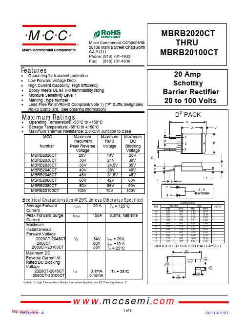
TM
Micro Commercial Components
omponents 20736 Marilla Street Chatsworth
!"# $
% !"#
Features
Tube: 1Kpcs/Box
***IMPORTANT NOTICE***
Micro Commercial Components Corp. reserves the right to make changes without further notice to any product herein to make corrections, modifications , enhancements , improvements , or other changes . Micro Commercial Components Corp . does not assume any liability arising out of the application or use of any product described herein; neither does it convey any license under its patent rights ,nor the rights of others . The user of products in such applications shall assume all risks of such use and will agree to hold Micro Commercial Components Corp . and all the companies whose products are represented on our website, harmless against all damages.
MBR20H200CT_07资料
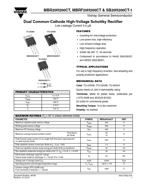
MBR20H200CT, MBRF20H200CT & SB20H200CT-1Vishay General SemiconductorDocument Number: Dual Common-Cathode High-Voltage Schottky RectifierLow Leakage Current 5.0 µAFEATURES•Guarding for overvoltage protection •Low power loss, high efficiency•Low forward voltage drop •High frequency operation•Solder dip 260 °C, 40 seconds•Component in accordance to RoHS 2002/95/EC and WEEE 2002/96/EC TYPICAL APPLICATIONSFor use in high frequency inverters, free-wheeling and polarity protection applications.MECHANICAL DATACase: TO-220AB, ITO-220AB, TO-262AA Epoxy meets UL 94V-0 flammability ratingTerminals: Matte tin plated leads, solderable per J-STD-002B and JESD22-B102D E3 suffix for commercial grade Mounting Torque: 10 in-lbs maximum Polarity: As markedPRIMARY CHARACTERISTICSI F(AV) 2 x 10 A V RRM 200 V I FSM 290 A V F 0.75 V T j175 °CTO-262AA1122 33123ITO-220ABMAXIMUM RATINGS (T C = 25°C unless otherwise noted)PARAMETER SYMBOL MBR20H200CT UNITMaximum repetitive peak reverse voltage V RRM 200 V Working peak reverse voltage V RWM 200 V Maximum DC blocking voltageV DC 200 V Maximum average forward rectified currentT otal deviceper diodeI F(AV) 2010 A Peak forward surge current 8.3 ms single half sine-wave superimposed on rated load per diodeI FSM290APeak repetitive reverse current per diode at t p = 2 µs, 1 kHzI RRM 1.0 A Peak non-repetitive reverse surge energy per diode (8/20 µs waveform) E RSM 20 mJ Non-repetitive avalanche energy per diode at 25 °C, I AS = 2.0 A, L = 10 mH E AS 20 mJ Electrostatic discharge capacitor voltageHuman body model air discharge: C = 100 pF , R 0 1.5 k ΩV C 25 KVVoltage rate of change (rated V R ) dv/dt 10000 V/µs Operating junction and storage temperature range T J , T STG- 65 to + 175°C Isolation voltage (ITO-220AB only)From terminals to heatsink t = 1 minute V AC 1500VMBR20H200CT, MBRF20H200CT & SB20H200CT-1Vishay General Semiconductor Document Number: 88786Note:(1) Pulse test: 300 µs pulse width, 1 % duty cycleRATINGS AND CHARACTERISTICS CURVES (T A = 25 °C unless otherwise noted)ELECTRICAL CHARACTERISTICS (T C = 25°C unless otherwise noted)PARAMETER TE S T CONDITION S SYMBOL TYP. MAX. UNITMaximum instantaneous forward voltage per diode (1)at I F = 10 A, T C = 25 °C at I F = 10 A, T C= 125 °C at I F = 20 A, T C = 25 °C at I F = 20 A, T C = 125 °CV F0.810.65 0.87 0.740.88 0.75 0.97 0.85VMaximum reverse current perdiode at working peak reverse voltage (1)T J= 25 °CT J = 125 °CI R5.0 1.0µA mA Typical junction capacitance at 4.0 V , 1 MHzCJ 250pFTHERMAL CHARACTERISTICS (T C = 25°C unless otherwise noted)PARAMETER S YMBOL MBR MBRF SB UNITTypical thermal resistance per diode R θJC 2.0 4.0 2.0°C/WORDERING INFORMATION (Example)PACKAGE PREFERRED P/N UNIT WEIGHT (g)PACKAGE CODEBASE QUANTITYDELIVERY MODETO-220AB MBR20H200CT -E3/45 2.064550/Tube T ube ITO-220AB MBRF20H200CT -E3/45 2.204550/Tube T ube TO-262AASB20H200CT -1E3/451.584550/TubeT ubeFigure 1. Forward Derating Curve (Total)Figure 2. Maximum Non-Repetitive Peak Forward SurgeCurrent Per DiodeMBR20H200CT, MBRF20H200CT & SB20H200CT-1Vishay General SemiconductorDocument Number: Figure 3. Typical Instantaneous Forward Characteristics Per Diode Figure 4. Typical Reverse Characteristics Per DiodeFigure 5. Typical Junction Capacitance Per DiodeFigure 6. Typical Transient Thermal Impedance Per DiodeMBR20H200CT, MBRF20H200CT & SB20H200CT-1Vishay General Semiconductor Document Number: 88786PACKAGE OUTLINE DIMENSIONS in inches (millimeters)Legal Disclaimer NoticeVishay Document Number: NoticeSpecifications of the products displayed herein are subject to change without notice. Vishay Intertechnology, Inc., or anyone on its behalf, assumes no responsibility or liability for any errors or inaccuracies.Information contained herein is intended to provide a product description only. No license, express or implied, by estoppel or otherwise, to any intellectual property rights is granted by this document. Except as provided in Vishay's terms and conditions of sale for such products, Vishay assumes no liability whatsoever, and disclaims any express or implied warranty, relating to sale and/or use of Vishay products including liability or warranties relating to fitness for a particular purpose, merchantability, or infringement of any patent, copyright, or other intellectual property right.The products shown herein are not designed for use in medical, life-saving, or life-sustaining applications.Customers using or selling these products for use in such applications do so at their own risk and agree to fully indemnify Vishay for any damages resulting from such improper use or sale.元器件交易网。
MBR10H100CTG资料
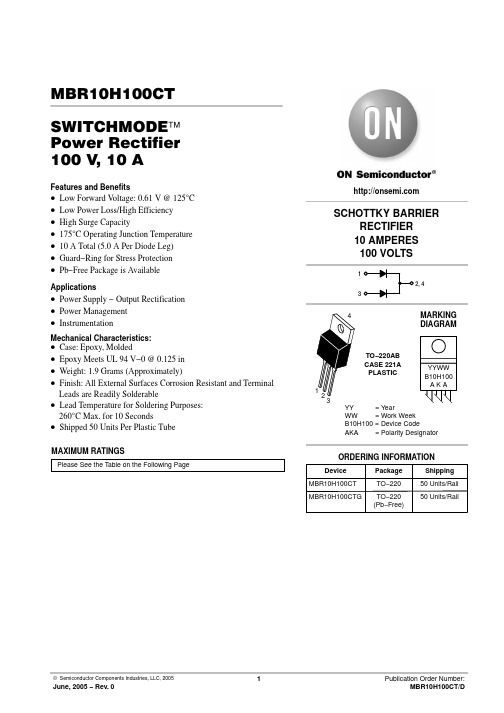
MBR10H100CTSWITCHMODE™Power Rectifier 100 V, 10 AFeatures and Benefits•Low Forward V oltage: 0.61 V @ 125°C •Low Power Loss/High Efficiency •High Surge Capacity•175°C Operating Junction Temperature •10 A Total (5.0 A Per Diode Leg)•Guard−Ring for Stress Protection •Pb−Free Package is Available Applications•Power Supply − Output Rectification •Power Management •InstrumentationMechanical Characteristics:•Case: Epoxy, Molded•Epoxy Meets UL 94 V−0 @ 0.125 in•Weight: 1.9 Grams (Approximately)•Finish: All External Surfaces Corrosion Resistant and Terminal Leads are Readily Solderable•Lead Temperature for Soldering Purposes:260°C Max. for 10 Seconds•Shipped 50 Units Per Plastic TubeMAXIMUM RATINGSPlease See the Table on the Following PageTO−220ABCASE 221APLASTICSCHOTTKY BARRIERRECTIFIER10 AMPERES100 VOLTS132, 4MARKINGDIAGRAMYY= YearWW= Work WeekB10H100= Device CodeAKA= Polarity DesignatorDevice Package Shipping ORDERING INFORMATIONMBR10H100CT TO−22050 Units/Rail MBR10H100CTG TO−220(Pb−Free)50 Units/RailMAXIMUM RATINGS (Per Diode Leg)Rating Symbol Value UnitPeak Repetitive Reverse Voltage Working Peak Reverse Voltage DC Blocking Voltage V RRMV RWMV R100VAverage Rectified Forward Current(Rated V R) T C = 168°CI F(AV) 5.0APeak Repetitive Forward Current(Rated V R, Square Wave, 20 kHz) T C = 165°CI FRM10ANonrepetitive Peak Surge Current(Surge applied at rated load conditions halfwave, single phase, 60 Hz)I FSM180A Operating Junction Temperature (Note 1)T J+175°C Storage Temperature T stg*65 to +175°C Voltage Rate of Change (Rated V R)dv/dt10,000V/m s Controlled Avalanche Energy (see test conditions in Figures 10 and 11)W AVAL100mJESD Ratings:Machine Model = CHuman Body Model = 3B> 400> 8000VTHERMAL CHARACTERISTICSMaximum Thermal Resistance− Junction−to−Case− Junction−to−Ambient R q JCR q JA2.060°C/WELECTRICAL CHARACTERISTICS (Per Diode Leg)Maximum Instantaneous Forward Voltage (Note 2) (I F = 5.0 A, T C = 25°C)(I F = 5.0 A, T C = 125°C)(I F = 10 A, T C = 25°C)(I F = 10 A, T C = 125°C)v F0.730.610.850.71VMaximum Instantaneous Reverse Current (Note 2) (Rated DC Voltage, T C = 125°C)(Rated DC Voltage, T C = 25°C)i R4.50.0035mAMaximum ratings are those values beyond which device damage can occur. Maximum ratings applied to the device are individual stress limit values (not normal operating conditions) and are not valid simultaneously. If these limits are exceeded, device functional operation is not implied, damage may occur and reliability may be affected.1.The heat generated must be less than the thermal conductivity from Junction−to−Ambient: dP D/dT J < 1/R q JA.2.Pulse Test: Pulse Width = 300 m s, Duty Cycle ≤2.0%.I F , I N S T A N T A N E O U S F O R W A R D C U R R E N T (A M P S )10010.1I R , R E V E R S E C U R R E N T (A M P S )I F , A V E R A G E F O R W A R D C U R R E N T (A M P S )Figure 5. Current DeratingT C , CASE TEMPERATURE (°C)120110105014015013016015I O , AVERAGE FORWARD CURRENT (AMPS)510Figure 6. Forward Power Dissipation10170180100S )C , C A P A C I T A N C E (p F )V R , REVERSE VOLTAGE (VOLTS)100104080Figure 7. Capacitance10020601000R (t ), T R A N S I E N T T H E R M A L R E S I S T A N C ER (t ), T R A N S I E N T T H E R M A L R E S I S T A N C EFigure 9. Thermal Response Junction−to−Caset 1, TIME (sec)BV DUTI L I DV DDt0t1t2t Figure 10. Test Circuit Figure 11. Current−Voltage WaveformsThe unclamped inductive switching circuit shown in Figure 10 was used to demonstrate the controlled avalanche capability of this device. A mercury switch was used instead of an electronic switch to simulate a noisy environment when the switch was being opened.When S1 is closed at t0 the current in the inductor I L ramps up linearly; and energy is stored in the coil. At t1 the switch is opened and the voltage across the diode under test begins to rise rapidly, due to di/dt effects, when this induced voltage reaches the breakdown voltage of the diode, it is clamped at BV DUT and the diode begins to conduct the full load current which now starts to decay linearly through the diode, and goes to zero at t2.By solving the loop equation at the point in time when S1 is opened; and calculating the energy that is transferred to the diode it can be shown that the total energy transferred is equal to the energy stored in the inductor plus a finite amount of energy from the V DD power supply while the diode is in breakdown (from t1 to t2) minus any losses due to finite component resistances. Assuming the component resistive elements are small Equation (1) approximates the total energy transferred to the diode. It can be seen from this equation that if the V DD voltage is low compared to the breakdown voltage of the device, the amount of energy contributed by the supply during breakdown is small and the total energy can be assumed to be nearly equal to the energy stored in the coil during the time when S1 was closed, Equation (2).W AVAL[12LI2LPKǒBV DUTBV DUT–V DDǓW AVAL[1LI2LPKEQUATION (1):EQUATION (2):PACKAGE DIMENSIONSTO−220PLASTICCASE 221A−09ISSUE AASWITCHMODE is a trademark of Semiconductor Components Industries, LLC.ON Semiconductor and are registered trademarks of Semiconductor Components Industries, LLC (SCILLC). SCILLC reserves the right to make changes without further notice to any products herein. SCILLC makes no warranty, representation or guarantee regarding the suitability of its products for any particular purpose, nor does SCILLC assume any liability arising out of the application or use of any product or circuit, and specifically disclaims any and all liability, including without limitation special, consequential or incidental damages.“Typical” parameters which may be provided in SCILLC data sheets and/or specifications can and do vary in different applications and actual performance may vary over time. All operating parameters, including “Typicals” must be validated for each customer application by customer’s technical experts. SCILLC does not convey any license under its patent rights nor the rights of others. SCILLC products are not designed, intended, or authorized for use as components in systems intended for surgical implant into the body, or other applications intended to support or sustain life, or for any other application in which the failure of the SCILLC product could create a situation where personal injury or death may occur. Should Buyer purchase or use SCILLC products for any such unintended or unauthorized application, Buyer shall indemnify and hold SCILLC and its officers, employees, subsidiaries, affiliates, and distributors harmless against all claims, costs, damages, and expenses, and reasonable attorney fees arising out of, directly or indirectly, any claim of personal injury or death associated with such unintended or unauthorized use, even if such claim alleges that SCILLC was negligent regarding the design or manufacture of the part. SCILLC is an Equal Opportunity/Affirmative Action Employer. This literature is subject to all applicable copyright laws and is not for resale in any manner.PUBLICATION ORDERING INFORMATION。
- 1、下载文档前请自行甄别文档内容的完整性,平台不提供额外的编辑、内容补充、找答案等附加服务。
- 2、"仅部分预览"的文档,不可在线预览部分如存在完整性等问题,可反馈申请退款(可完整预览的文档不适用该条件!)。
- 3、如文档侵犯您的权益,请联系客服反馈,我们会尽快为您处理(人工客服工作时间:9:00-18:30)。
MCC
Figure 2 Forward Derating Curve
120
80
Single Phase, Half Wave 60Hz Resistive or Inductive Load 0 50 70 90 °C 110 130 150
Average Forward Rectified Current - Amperes versus Case Temperature - °C
DIM A B C D E F G H J K L M DIMENSIONS INCH ES MIN MAX 3.150 NOM 1.565 1.585 .700 .800 2.400 2.500 .119 .132 1.375 REF 3.550 3.650 .580 .620 1/4 -20 UNF .380 .410 .185 .195 .275 .295 MM MIN MAX 80.01 NOM 39.75 40.26 17.78 20.32 60.96 63.50 3.02 3.35 34.92 REF 90.17 92.71 14.73 15.75 FULL 9.65 10.41 4.70 4.95 6.99 7.49
A B K C M J F D H E L
G
Electrical Characteristics @ 25°C Unless Otherwise Specified
Average Forward Current Peak Forward Surge Current Maximum Instantaneous Forward Voltage 20020-20045CT 20060CT 20080-200100CT Maximum DC Reverse Current At Rated DC Blocking Voltage Typical Junction Capacitance IF(AV) IFSM 200 A 1500A TC = 136°C 8.3ms, half sine
Figure 3 Junction Capacitance
10000 6000 4000 2000 pF TJ=25°C 1000 600 400 200 100 .1 .2 .4 1 Volts 2 4 10 20 40 100 200 400 1000
Junction Capacitance - pF versus Reverse Voltage - Volts
MCC Part Number MBR20020CT MBR20030CT MBR20035CT MBR20040CT MBR20045CT MBR20060CT MBR20080CT MBR200100CT
Maximum RMS Voltage 14V 21V 24.5V 28V 31.5V 42V 56V 70V
MCC
Figure 5 Peak Forward Surge Current
6
8 10 20 Cycles
40
60 80 100
Peak Forward Surge Current - Amperes versus Number Of Cycles At 60Hz - Cycles
Maximum Ratings
• • Operating Temperature: -55°C to +175°C Storage Temperature: -55°C to +175°C Maximum Recurrent Peak Reverse Voltage 20V 30V 35V 40V 45V 60V 80V 100V Maximum DC Blocking Voltage 20V 30V 35V 40V 45V 60V 80V 100V
元器件交易网
MBR20020CT thru MBR200100CT
Figure 4 Typical Reverse Characteristics 1000 600 400 1200 200 100 60 40 20 mAmps 10 6.0 4.0 2.0 1.0 .6 .4 .2 .1 10 20 TJ=25°C 40 60 Volts Instantaneous Reverse Leakage Current - MicroAmperes versus Percent Of Rated Peak Reverse Voltage - Volts 80 100 120 TJ=125°C 0 1 2 4 Amps 900 600 300 100 1500
THRU MBR200100CT
200 Amp Schottky Barrier Rectifier 20 to 100 Volts FULL PACK
Metal of siliconrectifier, majonty carrier conducton Guard ring for transient protection Low power loss high efficiency High surge capacity, High current capability
元器件交易网
MBR20020CT thru MBR200100CT
Figure 1 Typical Forward Characteristics 2000 1000 600 400 200 25°C Amps 100 60 40 20 10 6 4 2 1 0.2 0.4 0.6 Volts Instantaneous Forward Current - Amperes versus Instantaneous Forward Voltage - Volts 0.8 1.0 1.2 0 20 Amps 40 MBR20080CT-200100CT 160 MBR20020CT-20045CT MBR20060CT 200
元器件交易网
MCC
Features
• • • •
MBR20020CT
omponents 21201 Itasca Street Chatsworth !"# $
% !"#NOTE NhomakorabeaVF
.68 V .75 V .84 V
5 mA 75 mA
IFM = 100 A; TJ = 25°C
IR
TJ = 25°C TJ = 125°C
∅ ∅ ∅
CJ
4600pF Measured at 1.0MHz, VR=5.0V
*Pulse Test: Pulse Width 300µsec, Duty Cycle 2%
