AT45D041中文技术说明
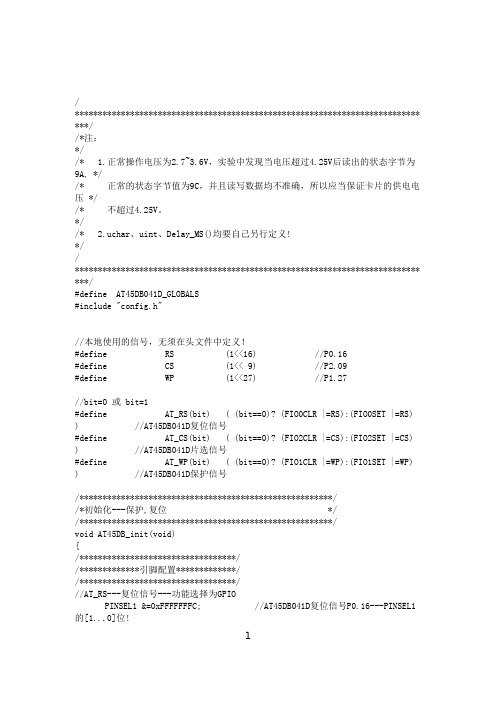
8051 模拟spi读写 AT45DB041

/*参数: */
unsigned char i;
for(i=0;i<8;i++){
if((wByte<<i)&0x80){SPI_SI=1;}
else{SPI_SI=0;}
SPI_SCK=0;
/* bit1 */
/* bit0 - 这2位暂时无效 */
/* bit5 */
/* bit4 */
SPI_HostWriteByte((unsigned char)(PA>>7));
SPI_HostWriteByte((unsigned char)((PA<<1)|(BFA>>8)));
SPI_HostWriteByte((unsigned char)BFA);
/* continue reading back at the beginning of the first page of memory.As w-*/
/* ith crossing over page boundaries,no delays will be incurred when wrapp-*/
/* first. */
/* 2005-06-02*/
/* nd clocked out of the device on the falling edge of SCK.All instruction-*/
/* s,addresses and data are transferred with the most significant bit(MSB) */
电能表可靠性技术论文
电能表可靠性技术研究【摘要】针对电能表可靠性技术研究问题,文中介绍了电能表硬件设计技术,主要有电能表电源管理监测、电能表输入信号滤波,探讨了电能表数据存储技术操作,分析了电能表电源监测电路及其原理,讨论决定电能表存储寿命因素,给出电能表存储结构和算法以提高寿命和靠性。
【关键词】多功能电能表;数据可靠性;数据存储0 引言多功能电能表可靠性技术,主要是可以准确提供多功能电能表检测电力线路的电流、电压信号,计算电流、电压、有功功率、无功功率,从而得到多功能电能表有功电能、无功电能,并保存在存储器中,给多功能电能表用户计量结算、状态检测提供依据。
多功能电能表可靠性技术的计算结果分为两大类:一是,暂时的、无需掉电保持的数据保,如电流、电压、功率等参数,可保存在随机存取存储器 ram中。
二是,需要长期保存的、掉电保持的数据,主要是多功能电能表的电能数据,必须存储到非易失性存储器中—通常采用flash闪存。
为保证多功能电能表在检测、采样、存取过程中信号完整性及数据可靠性,尤其是多功能电能表数据存取可靠性技术,需要从硬件和软件两个方面都采取措施,相互配合共同实现。
本文基于多功能电能表专用电能计量芯片att7022b,采用单片机pic16f77以及存储器 at45d041,研制了三相多功能电能表,现就将相关多功能电能表数据可靠技术进行探讨。
1 多功能电能表硬件设计技术多功能电能表硬件方面的可靠性技术主要包括电源监测管理以及输入信号的滤波调理的相关技术。
1.1 多功能电能表电源管理监测多功能电能表应用的单片机、att7022b、存储器等器件都只能在可靠的、有效的电源下才能工作。
多功能电能表的要求标准高,电源方案包括变压、整流、滤波、稳压等电路。
在三相电能表中,只要有一相电源供电,多功能电能表就必须工作,故使用三个单相变压器分别对三相电源输入进行隔离变压,再经过三个单相桥整流后并联输入电源管理与监测电路,此时可以得到多功能电能表稳定的直流电压 vz。
AT45DB041D-SU-2.5中文资料
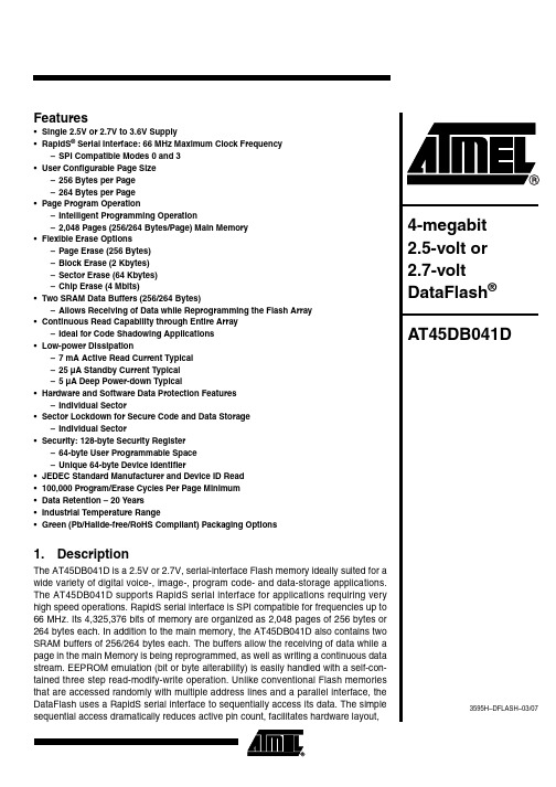
Features Array•Single 2.5V or 2.7V to 3.6V Supply•RapidS® Serial Interface: 66 MHz Maximum Clock Frequency–SPI Compatible Modes 0 and 3•User Configurable Page Size–256 Bytes per Page–264 Bytes per Page•Page Program Operation–Intelligent Programming Operation–2,048 Pages (256/264 Bytes/Page) Main Memory•Flexible Erase Options–Page Erase (256 Bytes)–Block Erase (2 Kbytes)–Sector Erase (64 Kbytes)–Chip Erase (4 Mbits)•Two SRAM Data Buffers (256/264 Bytes)–Allows Receiving of Data while Reprogramming the Flash Array•Continuous Read Capability through Entire Array–Ideal for Code Shadowing Applications•Low-power Dissipation–7 mA Active Read Current Typical–25 µA Standby Current Typical–5 µA Deep Power-down Typical•Hardware and Software Data Protection Features–Individual Sector•Sector Lockdown for Secure Code and Data Storage–Individual Sector•Security: 128-byte Security Register–64-byte User Programmable Space–Unique 64-byte Device Identifier•JEDEC Standard Manufacturer and Device ID Read•100,000 Program/Erase Cycles Per Page Minimum•Data Retention – 20 Years•Industrial Temperature Range•Green (Pb/Halide-free/RoHS Compliant) Packaging Options1.DescriptionThe AT45DB041D is a 2.5V or 2.7V, serial-interface Flash memory ideally suited for a wide variety of digital voice-, image-, program code- and data-storage applications. The AT45DB041D supports RapidS serial interface for applications requiring very high speed operations. RapidS serial interface is SPI compatible for frequencies up to 66 MHz. Its 4,325,376 bits of memory are organized as 2,048 pages of 256 bytes or 264 bytes each. In addition to the main memory, the AT45DB041D also contains two SRAM buffers of 256/264 bytes each. The buffers allow the receiving of data while a page in the main Memory is being reprogrammed, as well as writing a continuous data stream. EEPROM emulation (bit or byte alterability) is easily handled with a self-con-tained three step read-modify-write operation. Unlike conventional Flash memories that are accessed randomly with multiple address lines and a parallel interface, the DataFlash uses a RapidS serial interface to sequentially access its data. The simplesequential access dramatically reduces active pin count, facilitates hardware layout,23595H–DFLASH–03/07AT45DB041Dincreases system reliability, minimizes switching noise, and reduces package size. The device is optimized for use in many commercial and industrial applications where high-density, low-pin count, low-voltage and low-power are essential.To allow for simple in-system reprogrammability, the AT45DB041D does not require high input voltages for programming. The device operates from a single power supply, 2.5V to 3.6V or 2.7V to 3.6V, for both the program and read operations. The AT45DB041D is enabled through the Serial Output (SO), and the Serial Clock (SCK).All programming and erase cycles are self-timed.2.Pin Configurations and PinoutsTable 2-1.Pin ConfigurationsSymbolName and FunctionAsserted StateTypeCS Chip Select: Asserting the CS pin selects the device. When the CS pin is deasserted, the device will be deselected and normally be placed in the standby mode (not Deep Power-Down mode), and the output pin (SO) will be in a high-impedance state. When the device is deselected, data will not be accepted on the input pin (SI).A high-to-low transition on the CS pin is required to start an operation, and a low-to-high transition is required to end an operation. When ending an internally self-timed operation such as a program or erase cycle, the device will not enter the standby mode until the completion of the operation.Low InputSCK Serial Clock: This pin is used to provide a clock to the device and is used to control the flow of data to and from the device. Command, address, and input data present on the SI pin is always latched on the rising edge of SCK, while output data on the SO pin is always clocked out on the falling edge of SCK.–InputSI Serial Input: The SI pin is used to shift data into the device. The SI pin is used for all data input includingcommand and address sequences. Data on the SI pin is always latched on the rising edge of SCK. If the SER/BYTE pin is always driven low, the SI pin should be a “no connect”.–InputSO Serial Output: The SO pin is used to shift data out from the device. Data on the SO pin is always clocked out on the falling edge of SCK. If the SER/BYTE pin is always driven low, the SO pin should be a “no connect”.–OutputWPWrite Protect: When the WP pin is asserted, all sectors specified for protection by the Sector Protection Register will be protected against program and erase operations regardless of whether the Enable Sector Protection command has been issued or not. The WP pin functions independently of the software controlled protection method. After the WP pin goes low, the content of the Sector Protection Register cannot be modified.If a program or erase command is issued to the device while the WP pin is asserted, the device will simply ignore the command and perform no operation. The device will return to the idle state once the CS pin has been deasserted. The Enable Sector Protection command and Sector Lockdown command, however, will be recognized by the device when the WP pin is asserted.The WP pin is internally pulled-high and may be left floating if hardware controlled protection will not be used. However, it is recommended that the WP pin also be externally connected to V CC whenever possible.Low InputRESET Reset: A low state on the reset pin (RESET) will terminate the operation in progress and reset the internal state machine to an idle state. The device will remain in the reset condition as long as a low level is present on the RESET pin. Normal operation can resume once the RESET pin is brought back to a high level.The device incorporates an internal power-on reset circuit, so there are no restrictions on the RESET pin during power-on sequences. If this pin and feature are not utilized it is recommended that the RESET pin be driven high externally.Low InputV CC Device Power Supply: The V CC pin is used to supply the source voltage to the device.Operations at invalid V CC voltages may produce spurious results and should not be attempted.–Power GNDGround: The ground reference for the power supply. GND should be connected to the system ground.–Ground33595H–DFLASH–03/07AT45DB041D3.Block DiagramFigure 2-1.MLF Top ViewFigure 2-2.SOIC Top View43595H–DFLASH–03/07AT45DB041D4.Memory ArrayTo provide optimal flexibility, the memory array of the AT45DB041D is divided into three levels of granularity comprising of sectors, blocks, and pages. The “Memory Architecture Diagram” illus-trates the breakdown of each level and details the number of pages per sector and block. All program operations to the DataFlash occur on a page-by-page basis. The erase operations can be performed at the chip, sector, block or page level.Figure 4-1.Memory Architecture Diagram5.Device OperationThe device operation is controlled by instructions from the host processor. The list of instructions and their associated opcodes are contained in Tables 15-1 through 15-7. A valid instruction starts with the falling edge of CS followed by the appropriate 8-bit opcode and the desired buffer loading of the opcode and the desired buffer or main memory address location through the SI (serial input) pin. All instructions, addresses, and data are transferred with the most significant bit (MSB) first.Buffer addressing for the DataFlash standard page size (264 bytes) is referenced in the datasheet using the terminology BEA8 - BFA0 to denote the 9 address bits required to designate a byte address within a buffer. Main memory addressing is referenced using the terminology PA10 - PA0 and BA8 - BA0, where PA10 - PA0 denotes the 11 address bits required to desig-nate a page address and BA8 - BA0 denotes the 9 address bits required to designate a byte address within the page.For the “Power of 2” binary page size (256 bytes), the Buffer addressing is referenced in the datasheet using the conventional terminology BFA7 - BFA0 to denote the 8 address bits required to designate a byte address within a buffer. Main memory addressing is referenced using the terminology A18 - A0, where A18 - A8 denotes the 11 address bits required to desig-nate a page address and A7 - A0 denotes the 8 address bits required to designate a byte address within a page.53595H–DFLASH–03/07AT45DB041D6.Read CommandsBy specifying the appropriate opcode, data can be read from the main memory or from either one of the two SRAM data buffers. The DataFlash supports RapidS protocols for Mode 0 and Mode 3. Please refer to the “Detailed Bit-level Read Timing” diagrams in this datasheet for details on the clock cycle sequences for each mode.6.1Continuous Array Read (Legacy Command – E8H): Up to 66 MHzBy supplying an initial starting address for the main memory array, the Continuous Array Read command can be utilized to sequentially read a continuous stream of data from the device by simply providing a clock signal; no additional addressing information or control signals need to be provided. The DataFlash incorporates an internal address counter that will automatically increment on every clock cycle, allowing one continuous read operation without the need of additional address sequences. To perform a continuous read from the DataFlash standard page size (264 bytes), an opcode of E8H must be clocked into the device followed by three address bytes (which comprise the 24-bit page and byte address sequence) and 4 don’t care bytes. The first 11 bits (PA10-PA0) of the 20-bit address sequence specify which page of the main mem-ory array to read, and the last 9 bits (BA8-BA0) of the 20-bit address sequence specify the starting byte address within the page. To perform a continuous read from the binary page size (256 bytes), the opcode (E8H) must be clocked into the device followed by three address bytes and 4 don’t care bytes. The first 11 bits (A18 - A8) of the 19-bits sequence specify which page of the main memory array to read, and the last 8 bits (A7 - A0) of the 19-bits address sequence specify the starting byte address within the page. The don’t care bytes that follow the address bytes are needed to initialize the read operation. Following the don’t care bytes, additional clock pulses on the SCK pin will result in data being output on the SO (serial output) pin.The CS pin must remain low during the loading of the opcode, the address bytes, the don’t care bytes, and the reading of data. When the end of a page in main memory is reached during a Continuous Array Read, the device will continue reading at the beginning of the next page with no delays incurred during the page boundary crossover (the crossover from the end of one page to the beginning of the next page). When the last bit in the main memory array has been read,the device will continue reading back at the beginning of the first page of memory. As with cross-ing over page boundaries, no delays will be incurred when wrapping around from the end of the array to the beginning of the array.pin (SO). The maximum SCK frequency allowable for the Continuous Array Read is defined by the f CAR1 specification. The Continuous Array Read bypasses both data buffers and leaves the contents of the buffers unchanged.6.2Continuous Array Read (High Frequency Mode – 0BH): Up to 66 MHzThis command can be used with the serial interface to read the main memory array sequentially in high speed mode for any clock frequency up to the maximum specified by f CAR1. To perform a opcode 0BH must be clocked into the device followed by three address bytes and a dummy byte. The first 11 bits (PA10 - PA0) of the 20-bit address sequence specify which page of the main memory array to read, and the last 9 bits (BA8 - BA0) of the 20-bit address sequence spec-ify the starting byte address within the page. To perform a continuous read with the page size set to 256 bytes, the opcode, 0BH, must be clocked into the device followed by three address bytes (A18 - A0) and a dummy byte. Following the dummy byte, additional clock pulses on the SCK pin will result in data being output on the SO (serial output) pin.63595H–DFLASH–03/07AT45DB041DThe CS pin must remain low during the loading of the opcode, the address bytes, and the read-ing of data. When the end of a page in the main memory is reached during a Continuous Array Read, the device will continue reading at the beginning of the next page with no delays incurred during the page boundary crossover (the crossover from the end of one page to the beginning of the next page). When the last bit in the main memory array has been read, the device will con-tinue reading back at the beginning of the first page of memory. As with crossing over page boundaries, no delays will be incurred when wrapping around from the end of the array to the beginning of the array. A low-to-high transition on the CS pin will terminate the read operation and tri-state the output pin (SO). The maximum SCK frequency allowable for the Continuous Array Read is defined by the f CAR1 specification. The Continuous Array Read bypasses both data buffers and leaves the contents of the buffers unchanged.6.3Continuous Array Read (Low Frequency Mode: 03H): Up to 33 MHzThis command can be used with the serial interface to read the main memory array sequentially without a dummy byte up to maximum frequencies specified by f CAR2. To perform a continuous 03H, must be clocked into the device followed by three address bytes (which comprise the 24-bit page and byte address sequence). The first 11 bits (PA10 - PA0) of the 20-bit address sequence specify which page of the main memory array to read, and the last 9 bits (BA8 - BA0) of the 20-bit address sequence specify the starting byte address within the page. To perform a contin-uous read with the page size set to 256 bytes, the opcode, 03H, must be clocked into the device followed by three address bytes (A18 - A0). Following the address bytes, additional clock pulses on the SCK pin will result in data being output on the SO (serial output) pin.The CS pin must remain low during the loading of the opcode, the address bytes, and the read-ing of data. When the end of a page in the main memory is reached during a Continuous Array Read, the device will continue reading at the beginning of the next page with no delays incurred during the page boundary crossover (the crossover from the end of one page to the beginning of the next page). When the last bit in the main memory array has been read, the device will con-tinue reading back at the beginning of the first page of memory. As with crossing over page boundaries, no delays will be incurred when wrapping around from the end of the array to the beginning of the array. A low-to-high transition on the CS pin will terminate the read operation and tri-state the output pin (SO). The Continuous Array Read bypasses both data buffers and leaves the contents of the buffers unchanged.6.4Main Memory Page ReadA main memory page read allows the user to read data directly from any one of the 2,048 pages in the main memory, bypassing both of the data buffers and leaving the contents of the buffers unchanged. To start a page read from the DataFlash standard page size (264 bytes), an opcode of D2H must be clocked into the device followed by three address bytes (which comprise the 24-bit page and byte address sequence) and 4 don’t care bytes. The first 11 bits (PA10-PA0) of the 20-bit address sequence specify the page in main memory to be read, and the last 9 bits (BA8-BA0) of the 20-bit address sequence specify the starting byte address within that page.To start a page read from the binary page size (256 bytes), the opcode D2H must be clocked into the device followed by three address bytes and 4 don’t care bytes. The first 11 bits (A18 - A8) of the 19-bits sequence specify which page of the main memory array to read, and the last 8 bits (A7 - A0) of the 19-bits address sequence specify the starting byte address within the page. The don’t care bytes that follow the address bytes are sent to initialize the read opera-tion. Following the don’t care bytes, additional pulses on SCK result in data being output on the SO (serial output) pin. The CS pin must remain low during the loading of the opcode, the address bytes, the don’t care bytes, and the reading of data. When the end of a page in main73595H–DFLASH–03/07AT45DB041Dmemory is reached, the device will continue reading back at the beginning of the same page. A low-to-high transition on the CS pin will terminate the read operation and tri-state the output pin (SO). The maximum SCK frequency allowable for the Main Memory Page Read is defined by the f SCK specification. The Main Memory Page Read bypasses both data buffers and leaves the contents of the buffers unchanged.6.5Buffer ReadThe SRAM data buffers can be accessed independently from the main memory array, and utiliz-ing the Buffer Read Command allows data to be sequentially read directly from the buffers. Four opcodes, D4H or D1H for buffer 1 and D6H or D3H for buffer 2 can be used for the Buffer Read Command. The use of each opcode depends on the maximum SCK frequency that will be used to read data from the buffer. The D4H and D6H opcode can be used at any SCK frequency up to the maximum specified by f CAR1. The D1H and D3H opcode can be used for lower frequency read operations up to the maximum specified by f CAR2.To perform a buffer read from the DataFlash standard buffer (264 bytes), the opcode must be clocked into the device followed by three address bytes comprised of 15 don’t care bits and 9buffer address bits (BFA8-BFA0). To perform a buffer read from the binary buffer (256 bytes),the opcode must be clocked into the device followed by three address bytes comprised of 16don’t care bits and 8 buffer address bits (BFA7 - BFA0). Following the address bytes, one don’t care byte must be clocked in to initialize the read operation. The CS pin must remain low during the loading of the opcode, the address bytes, the don’t care bytes, and the reading of data. When the end of a buffer is reached, the device will continue reading back at the beginning the output pin (SO).7.Program and Erase Commands7.1Buffer WriteData can be clocked in from the input pin (SI) into either buffer 1 or buffer 2. To load data into the DataFlash standard buffer (264 bytes), a 1-byte opcode, 84H for buffer 1 or 87H for buffer 2,must be clocked into the device, followed by three address bytes comprised of 15 don’t care bits and 9 buffer address bits (BFA8-BFA0). The 9 buffer address bits specify the first byte in the buffer to be written. To load data into the binary buffers (256 bytes each), a 1-byte opcode 84H for buffer 1 or 87H for buffer 2, must be clocked into the device, followed by three address bytes comprised of 16 don’t care bits and 8 buffer address bits (BFA7 - BFA0). The 8 buffer address bits specify the first byte in the buffer to be written. After the last address byte has been clocked into the device, data can then be clocked in on subsequent clock cycles. If the end of the data buffer is reached, the device will wrap around back to the beginning of the buffer. Data will con-7.2Buffer to Main Memory Page Program with Built-in EraseData written into either buffer 1 or buffer 2 can be programmed into the main memory. A 1-byte opcode, 83H for buffer 1 or 86H for buffer 2, must be clocked into the device. For the DataFlash standard page size (264 bytes), the opcode must be followed by three address bytes consist of 4 don’t care bits, 11 page address bits (PA10 - PA0) that specify the page in the main memory to be written and 9 don’t care bits. To perform a buffer to main memory page program with built-in erase for the binary page size (256 bytes), the opcode 83H for buffer 1 or 86H for buffer 2, must be clocked into the device followed by three address bytes consisting of 5 don’t care bits83595H–DFLASH–03/07AT45DB041D11page address bits (A18 - A8) that specify the page in the main memory to be written and 8don’t care bits. When a low-to-high transition occurs on the CS pin, the part will first erase the selected page in main memory (the erased state is a logic 1) and then program the data stored in the buffer into the specified page in main memory. Both the erase and the programming of the page are internally self-timed and should take place in a maximum time of t EP . During this time,the status register will indicate that the part is busy.7.3Buffer to Main Memory Page Program without Built-in EraseA previously-erased page within main memory can be programmed with the contents of either buffer 1 or buffer 2. A 1-byte opcode, 88H for buffer 1 or 89H for buffer 2, must be clocked into the device. For the DataFlash standard page size (264 bytes), the opcode must be followed by three address bytes consist of 4 don’t care bits, 11 page address bits (PA10-PA0) that specify the page in the main memory to be written and 9 don’t care bits. To perform a buffer to main memory page program without built-in erase for the binary page size (256 bytes), the opcode 88H for buffer 1 or 89H for buffer 2, must be clocked into the device followed by three address bytes consisting of 5 don’t care bits, 11 page address bits (A18 - A8) that specify the page in the main memory to be written and 8 don’t care bits. When a low-to-high transition occurs on the CS pin, the part will program the data stored in the buffer into the specified page in the main mem-ory. It is necessary that the page in main memory that is being programmed has been previously erased using one of the erase commands (Page Erase or Block Erase). The programming of the page is internally self-timed and should take place in a maximum time of t P . During this time, the status register will indicate that the part is busy.7.4Page EraseThe Page Erase command can be used to individually erase any page in the main memory array allowing the Buffer to Main Memory Page Program to be utilized at a later time. To perform a page erase in the DataFlash standard page size (264bytes), an opcode of 81H must be loaded into the device, followed by three address bytes comprised of 4 don’t care bits, 11 page address bits (PA10-PA0) that specify the page in the main memory to be erased and 9 don’t care bits.To perform a page erase in the binary page size (256 bytes), the opcode 81H must be loaded into the device, followed by three address bytes consist of 5 don’t care bits, 11 page address bits (A18 - A8) that specify the page in the main memory to be erased and 8 don’t care bits. When a state is a logical 1). The erase operation is internally self-timed and should take place in a maxi-mum time of t PE . During this time, the status register will indicate that the part is busy.7.5Block EraseA block of eight pages can be erased at one time. This command is useful when large amounts of data has to be written into the device. This will avoid using multiple Page Erase Commands.To perform a block erase for the DataFlash standard page size (264bytes), an opcode of 50H must be loaded into the device, followed by three address bytes comprised of 4 don’t care bits,8page address bits (PA10 - PA3) and 12 don’t care bits. The 8 page address bits are used to specify which block of eight pages is to be erased. To perform a block erase for the binary page size (256 bytes), the opcode 50H must be loaded into the device, followed by three address bytes consisting of 5 don’t care bits, 8 page address bits (A18 - A11) and 11 don’t care bits. The 9 page address bits are used to specify which block of eight pages is to be erased. When a low-to-high transition occurs on the CS pin, the part will erase the selected block of eight pages. The erase operation is internally self-timed and should take place in a maximum time of t BE . During this time, the status register will indicate that the part is busy.93595H–DFLASH–03/07AT45DB041D7.6Sector EraseThe Sector Erase command can be used to individually erase any sector in the main memory.There are 8 sectors and only one sector can be erased at one time. To perform sector 0a or sec-tor 0b erase for the DataFlash standard page size (264 bytes), an opcode of 7CH must be loaded into the device, followed by three address bytes comprised of 4 don’t care bits, 8 page address bits (PA10 - PA3) and 12 don’t care bits. To perform a sector 1-7 erase, the opcode 7CH must be loaded into the device, followed by three address bytes comprised of 4 don’t care bits, 3 page address bits (PA10 - PA8) and 17 don’t care bits. To perform sector 0a or sector 0b erase for the binary page size (256 bytes), an opcode of 7CH must be loaded into the device,followed by three address bytes comprised of 5 don’t care bit and 8 page address bits (A18 -A11) and 11 don’t care bits. To perform a sector 1-15 erase, the opcode 7CH must be loaded into the device, followed by three address bytes comprised of 5 don’t care bit and 3 page address bits (A18 - A16) and 17 don’t care bits. The page address bits are used to specify any valid address location within the sector which is to be erased. When a low-to-high transition self-timed and should take place in a maximum time of t SE . During this time, the status register will indicate that the part is busy.Table 7-1.Block Erase AddressingPA10/A18PA9/A17PA8/A16PA7/A15PA6/A14PA5/A13PA4/A12PA3/A11PA2/A10PA1/A9PA0/A8Block 00000000X X X 000000001X X X 100000010X X X 200000011X X X 3••••••••••••••••••••••••••••••••••••11111100X X X 25211111101X X X 25311111110X X X 25411111111XXX255103595H–DFLASH–03/07AT45DB041D7.7Chip Erase (1)The entire main memory can be erased at one time by using the Chip Erase command.To execute the Chip Erase command, a 4-byte command sequence C7H, 94H, 80H and 9AH must be clocked into the device. Since the entire memory array is to be erased, no address bytes need to be clocked into the device, and any data clocked in after the opcode will be ignored. After the last bit of the opcode sequence has been clocked in, the CS pin can be deas-serted to start the erase process. The erase operation is internally self-timed and should take place in a time of t CE . During this time, the Status Register will indicate that the device is busy.The Chip Erase command will not affect sectors that are protected or locked down; the contents of those sectors will remain unchanged. Only those sectors that are not protected or locked down will be erased.The WP pin can be asserted while the device is erasing, but protection will not be activated until the internal erase cycle completes.Figure 7-1.Chip EraseNote: 1.Refer to the errata regarding Chip Erase on page 52.Table 7-2.Sector Erase AddressingPA10/A18PA9/A17PA8/A16PA7/A15PA6/A14PA5/A13PA4/A12PA3/A11PA2/A10PA1/A9PA0/A8Sector 00000000X X X 0a 00000001X X X 0b 001X X X X X X X X 1010X X X X X X X X 2••••••••••••••••••••••••••••••••••••100X X X X X X X X 4101X X X X X X X X 5110X X X X X X X X 6111XXXXXXXX7Command Byte 1Byte 2Byte 3Byte 4Chip EraseC7H94H80H9AHAT45DB041D7.8Main Memory Page Program Through BufferThis operation is a combination of the Buffer Write and Buffer to Main Memory Page Programwith Built-in Erase operations. Data is first clocked into buffer 1 or buffer 2 from the input pin (SI)and then programmed into a specified page in the main memory. To perform a main memorypage program through buffer for the DataFlash standard page size (264 bytes), a 1-byte opcode,82H for buffer 1 or 85H for buffer 2, must first be clocked into the device, followed by threeaddress bytes. The address bytes are comprised of 4 don’t care bits, 11 page address bits,(PA10-PA0) that select the page in the main memory where data is to be written, and 9 bufferaddress bits (BFA8-BFA0) that select the first byte in the buffer to be written. To perform amain memory page program through buffer for the binary page size (256 bytes), the opcode 82Hfor buffer 1 or 85H for buffer 2, must be clocked into the device followed by three address bytesconsisting of 5 don’t care bits, 11 page address bits (A18 - A8) that specify the page in the mainmemory to be written, and 8 buffer address bits (BFA7 - BFA0) that selects the first byte in thebuffer to be written. After all address bytes are clocked in, the part will take data from the inputpins and store it in the specified data buffer. If the end of the buffer is reached, the device willpin, the part will first erase the selected page in main memory to all 1s and then program thedata stored in the buffer into that memory page. Both the erase and the programming of thepage are internally self-timed and should take place in a maximum time of t EP. During this time,the status register will indicate that the part is busy.8.Sector ProtectionTwo protection methods, hardware and software controlled, are provided for protection againstinadvertent or erroneous program and erase cycles. The software controlled method relies onthe use of software commands to enable and disable sector protection while the hardware con-that are to be protected or unprotected against program and erase operations is specified in thenonvolatile Sector Protection Register. The status of whether or not sector protection has beenenabled or disabled by either the software or the hardware controlled methods can be deter-mined by checking the Status Register.。
ROM的选型

ROM的选型ROM用来存储程序代码,系统配置参数及系统运行过程中需要记录的各种信息。
目前常用的存储类型有Serial Flash、串行F-RAM、NAND Flash等。
FLASH:在线进行电擦写,掉电后信息不丢失的存储器。
低功耗、大容量,可整片或分扇区在线编程和擦除,通常用于存放程序代码、常量表以及一些在系统掉电后需要保存的用户数据等。
NOR和NAND是现在市场上两种主要的非易失闪存技术。
NOR FLASH的特点是芯片内执行(XIP,Execute In Place就位执行),这样应用程序可以直接在FLASH闪存内运行,不必再把代码读到系统RAM中。
NOR 的传输效率很高,在1~4MB的小容量时具有很高的成本效益,但是很低的写入和擦除速度大大影响了它的性能。
NAND结构能提供极高的存储单元密度,可以达到高存储密度,并且写入和擦除的速度也很快。
应用NAND的困难在于flash的管理和需要特殊的系统接口。
接口差别:NOR带有SRAM接口,有足够的地址引脚来寻址,可以很容易地存取其内部的每一个字节。
NAND器件使用复杂的I/O口来串行存取数据,各个产品或厂商的方法个不相同。
8个引脚用来传送控制、地址和数据信息。
NAND读和写操作采用512字节的块,这一点有点像硬盘管理此类操作,很自然地,基于NAND的存储器就可以取代硬盘或其他块设备。
容量和成本:NAND的单元尺寸几乎是NOR器件的一半,由于生产过程更为简单,NAND 结构可以在给定的模具尺寸内提供更高的容量,也就相应地降低了价格。
NOR占据了容量1-16MB闪存市场的大部分,而NAND只是用在8-128MB 的产品当中,这也就说明了NOR主要应用于代码存储介质中,NAND适合于数据存储,NAND在CompactFlash、Secure Digital、PC Cards和MMC存储卡市场上所占份额最大。
同时NAND受到位反转和坏块的影响其单元尺寸几乎是NOR FLASH的一半,由于生产过程更为简单,NAND结构可以在给定的模具尺寸内提供更高的容量,也就相应地降低了成本。
IC卡基础知识

所谓IC卡,就是集成电路卡,英文叫做Integrated Circuit Card。
目前市场上IC卡的种类很多,通常有以下几种分类方式:1.按组成结构分类:一般存储卡(Memory Card)、逻辑加密存储卡(Security Card)、CPU卡(Smart Card)。
一般存储卡实际上就是普通的EEPROM,不过是封装成module嵌入到卡片上了而已。
只要实现电气接触就可以对其内部数据进行无条件访问(当然需要根据该型号EEPROM的电气规范了)。
这种卡安全性几乎为0,所以只能用于一些对安全性不作要求的场合。
逻辑加密存储卡,这种IC卡中除了封装了上述EEPROM存储器外,还专设有逻辑加密电路,提供了硬件加密手段.因此不但存储量大,而且安全性强,不但可保证卡上存储数据读写安全, 而且能进行用户身份的认证. 由于密码不是在读写器软件中而是存储于IC卡上,所以几乎没有破密的可能性.例如:美国ATMEL1604逻辑加密卡,卡上设有三级保密功能.总密码用于身份的认证,非法用户三次密码核对错误即可使卡报废. 四个数据存储区可分别存储不同信息,又各和独立的读写密码.可以做到一卡多用, 在不同读写器件中核实相应密码进行某一业务操作,不会影响其它存储区.卡上信息不能随意改写,改写前需先擦除,而擦除需核对擦除需要核对擦除密码. 这样即使是持卡人自己也不能随意更改卡上数据.因此这种逻辑加密卡保密性极强,能自动识别读写器,持卡人和控制操作类型,常用于安全性要求高的场合。
CPU卡:又叫智能卡,Smart Card,这是真正的卡上单片机系统,CPU卡片内集成了中央处理器CPU, 程序存储器ROM, 数据存储器EEPROM 和RAM, 一般ROM 中还配有卡上操作系统软件COS(Chip operating system).CPU卡上的微处理器可以执行COS监控程序,接收从读写器送来的命令和数据, 分析命令后控制对存储器的访问.由于这种卡具有智能,读写器对卡的操作要经过卡上COS,所以保密性更强.而且微处理器具有数据加工和处理的能力,可以对读写数据进行逻辑和算术运算,能力很强.这种IC卡存储的数据对外相当于一个-黑盒子, 保密性极强.目前IC卡上用的微处理器一般为8位CPU,存储容量几十KB上下. 此种智能卡常用于重要场合,作为证件和信用卡。
几种常用IC卡的特性

几种常用IC卡的特性1. AT24C01A/02/04/08/16/64卡该系列IC卡均为非加密存储卡,容量分别为1K,2K,4K,8K,16K,64K bit,只有读、写两种操作。
2. AT45D041卡AT45D041卡是非加密存储卡,容量为4M bit,整卡分为2048页,每页有264 byte 。
只有读、写两种操作。
3. AT88SC102卡AT88SC102为加密存储卡,容量为1K bit。
整卡分两个应用区,容量均为64 byte。
熔丝熔断前,各区的读、写和擦除,受总密码和读写保护位的控制,数据按字节擦除;熔丝熔断后,各区的读、写和擦除,受总密码、读写属性控制位和擦除密码的控制,只要正确核对分区擦除密码,整区数据将自动擦除。
4. AT88SC1601/1604卡AT88SC1601是加密存储卡,容量为16K bit。
整卡分为一个公用区和四个应用区,个人化之前,整个卡的访问受总密码和读写保护位的控制。
个人化之后,各区的读、写和擦除都要受总密码、分区密码、分区擦除密码和读写保护位的控制。
1604 与1601卡基本相同,它们的区别是:各个分区的容量不同;1601只是1区有密码计数器,而1604的4个分区都有密码计数器。
5. SLE4432/4442卡SLE4442为加密存储卡,容量为256 byte。
总密码核对正确之后,才可以对卡读、写操作。
该卡前32字节可进行写保护位操作。
总密码错误计数器值为3,核对错误一次,减1操作,若计数值为0,整卡数据锁死。
若3次内有一次核对正确,则计数器恢复初值。
SLE4432特性与4442相似,但无密码操作功能。
6. SLE4418/4428卡SLE4428为加密存储卡,容量为1K byte。
总密码核对正确之后,才可以对卡读、写操作。
该卡所有数据均可以写保护(固化数据)。
总密码错误计数器值为8。
SLE4418特性与4428相似,但无密码操作功能。
7. SLE4404卡SLE 4404是加密存储卡,容量为52 byte。
接触式IC卡读写器使用手册

目录第一章 DP系列接触式IC卡读写器简介 (3)1.1概述 (3)1.2读写器型号 (3)1.3装箱清单 (4)1.4读写器连接方式.... (4)1.5指示灯 (4)1.6程序安装 (4)1.7用户软件 (4)1.8技术指标 (5)第二章演示系统使用说明 (6)第三章 IC卡读写器驱动程序函数说明 (9)3.1 安装程序主要目录和文件 (9)3.2 函数使用规则 (9)3.3 各种库函数说明 (9)3.3.1 C语言接口函数库 (9)●通用函数库 (10)●AT24C01A/24C02/24C04/24C08/24C16/24C64 (13)●AT45D041 (14)●AT88SC102/1604/1604B (15)●AT93C46/93C46A (22)●SLE4404 (23)●SLE4406 (26)●SLE4418/4428 (28)●SLE4432/4442 (30)●CPU卡 (30)3.3.2 FOXPRO FOR DOS函数库 (33)3.3.3 WINDOWS 16位和32位动态库 (34)3.3.4 FOXBASE函数库 (35)3.3.5UNIX函数库 (38)3.3.6LINUX函数库 (38)3.4 VFP、VB、Delphi和PB调用动态库的方法 (38)3.4.1 VFP调用16位动态库的方法 (38)3.4.2 VFP调用32位动态库的方法 (39)3.4.3 VB调用动态库的方法 (40)3.4.4 Delphi调用32位动态库的方法 (41)3.4.5 PB调用32位动态库的方法 (42)3.4.6 VC调用32位动态库的方法 (42)3.5 IC卡类型代码 (43)3.6 函数错误类型代码 (43)3.7自动卡型测试函数原理说明 (44)附录一几种常用IC卡的特性 (45)[2000/05/10]DP-R-XXX第一章DP系列接触式IC卡读写器简介1.1 概述深圳市明华澳汉科技有限公司是以生产IC卡及开发IC卡相关设备为主导产品的高新科技企业。
AT45xxx多路温度测试仪用户手册说明书

AT45xxx多路温度测试仪用户手册2安全须知当你发现有以下不正常情形发生,请立即终止操作并断开电源线。
立刻与安柏科技销售部联系维修。
否则将会引起火灾或对操作者有潜在的触电危险。
l仪器操作异常。
l操作中仪器产生反常噪音、异味、烟或闪光。
l操作过程中,仪器产生高温或电击。
l电源线、电源开关或电源插座损坏。
l杂质或液体流入仪器。
安全信息为避免可能的电击和人身安全,请遵循以下指南进行操作。
免责声明用户在开始使用仪器前请仔细阅读以下安全信息,对于用户由于未遵守下列条款而造成的人身安全和财产损失,安柏科技将不承担任何责任。
仪器接地为防止电击危险,请连接好电源地线。
不可在爆炸性气体环境使用仪器不可在易燃易爆气体、蒸汽或多灰尘的环境下使用仪器。
在此类环境使用任何电子设备,都是对人身安全的冒险。
不可打开仪器外壳非专业维护人员不可打开仪器外壳,以试图维修仪器。
仪器在关机后一段时间内仍存在未释放干净的电荷,这可能对人身造成电击危险。
不要使用已经损坏的仪器如果仪器已经损害,其危险将不可预知。
请断开电源线,不可再使用,也不要试图自行维修。
不要使用工作异常的仪器如果仪器工作不正常,其危险不可预知,请断开电源线,不可再使用,也不要试图自行维修。
不要超出本说明书指定的方式使用仪器超出范围,仪器所提供的保护措施将失效。
声明:!, $, #,安柏标志和文字是常州安柏精密仪器有限公司的商标或注册商标。
QQ:285480356 55178055AT45xxx多路温度测试仪用户手册User’s Manual简体中文Simplified ChineseRev.A2 2009/11 @Instruments 常州安柏精密仪器有限公司©2005-2009 Applent Instruments, Inc.目录 5目录安全须知 (2)安全信息 (2)有限担保和责任范围 (4)1.安装和设置向导 (9)1.1装箱清单 (9)1.2电源要求 (9)1.3操作环境 (9)1.4清洗 (9)1.5仪器手柄 (11)2.概述 (12)2.1引言 (12)2.2测量功能 (12)2.2.1测量参数 (12)2.2.2测试速度 (12)2.2.3基本准确度 (12)2.2.4测量显示范围 (13)2.3主要功能 (13)2.3.1比较器功能 (13)2.3.2用户校正功能 (13)2.3.3文件功能 (13)2.3.4系统设置 (13)2.3.5接口 (13)3.开始 (14)3.1认识前面板 (14)3.1.1前面板描述 (14)3.1.2认识后面板 (15)3.2上电启动 (15)3.2.1开机 (15)3.2.2开机值 (15)4.[Meas] 测量主页面 (16)4.1<测量显示>页 (16)4.1.1【型号】 (16)<测量显示>页的信息栏 (17)4.2<曲线图>页 (17)5.【Setup】设置主页面 (18)5.1功能设置 (18)5.1.1【比较器】 (18)5.1.2【速度】 (19)5.1.3【讯响】 (19)5.1.4【音量】 (19)5.1.5【通讯】 (19)5.1.6【波特率】 (20)5.1.7【字体】 (20)5.1.8【巡检】 (20)5.2分选设置 (21)6AT45xxx系列多路温度测试仪用户手册5.2.1【001】 (21)5.3用户校正 (22)5.3.1【001】 (22)5.4U盘设置 (23)5.4.1【创建文件】 (23)5.4.2【采样时间】 (23)5.4.3【文件操作】 (23)6.系统配置 (24)6.1系统配置页 (24)6.1.1更改系统语言【LANGUAGE】 (24)6.1.2修改日期和时间 (25)6.1.3帐号设置 (25)6.2系统信息页 (26)7.文件操作 (27)7.1文件管理 (27)7.1.1【自动保存】开关 (27)7.1.2文件操作 (28)7.1.3快捷操作文件 (28)8.规格 (29)8.1技术指标 (29)8.2一般规格 (29)8.3外形尺寸 (30)目录7插图目录图1-1仪器手柄(示意图,面板图形与实际不符) (11)图3-1 前面板 (14)图3-2后面板 (15)4-1 <测量显示>页 (16)图5-1<设置>页 (18)图6-1<系统配置>页 (24)图6-2<系统信息>页 (26)图7-1<文件管理>页 (27)8AT45xxx系列多路温度测试仪用户手册表格目录表3-1 前面板功能描述 (14)表4-1参数描述 (16)安装与设置向导91.安装和设置向导感谢您购买我公司的产品!使用前请仔细阅读本章。
常州市银联电子有限公司

常州市银联电子有限公司 客户订货指南二○○五年五月目录一、简介二、YLE-100系列串口扩展器三、YLE-200系列IC卡读写机四、YLE-300系列磁卡读写机五、YLE-400系列阅读器六、YLE-600系列卡头机芯七、YLE-700系列电话按键查询机八、YLE-750系列计算机按键查询机九、YLE-900系列密码键盘一、简介常州市银联电子有限公司是集科研开发,生产销售,计算机技术应用服务于一体的高科技企业。
银联电子主要生产密码键盘,免填单键盘,磁卡/条码阅读器,磁卡读写机,磁卡/条码委托查询机等产品。
产品通过各地的经销网络供应全国各地。
银联电子的生产工艺、品质检测全部按照ISO9002质量体系和企业标准进行,生产工艺先进,检测设施完善。
银联电子的部件类产品为满足各整机制造厂商对关键零部件的需求,采用专有技术,为客户开发、生产的OEM产品,由于实践了规模化及专业化生产,银联电子的制造成本较低,性能优良,品质稳定。
银联电子目前生产的整机类产品主要是磁卡、条码识读设备。
银联电子的整机产品中使用的关键零部件大部分都是自行设计、制造,具有自主知识产权。
产品设计合理,性能优良,可以满足客户的各种需求。
银联电子的产品为了配合国家“三金”工程建设,以及商业、邮政电子化的需求,将陆续通过各地的代理、分销机构满足国内客户日益增长的需求。
本手册主要目的是便于客户了解和掌握定购YLE系列的各类产品。
简要介绍了产品的特点、用途及型号规格。
详细内容请参阅有关的产品介绍及产品使用手册。
YLE产品型号一览表:产品型号 型号说明 功能简介串行口扩展器可将主机或终端的一个串口扩展成四个YLE-100系列 串口扩展器串行口。
YLE-200系列 IC卡读写机 读写多种Memory卡和逻辑加密卡,并配有有多种卡座。
YLE-300系列 磁卡读写机 读写多种磁条卡,具有读写普通抗磁和高抗磁型号。
YLE-400系列 磁卡、条码卡、ID卡阅读器 只读磁卡、条码卡、ID卡,具有多种接口输出。
机车供电系统数据读出软件使用说明(DF11G)
机车供电系统数据读出软件使用说明
一:软件说明
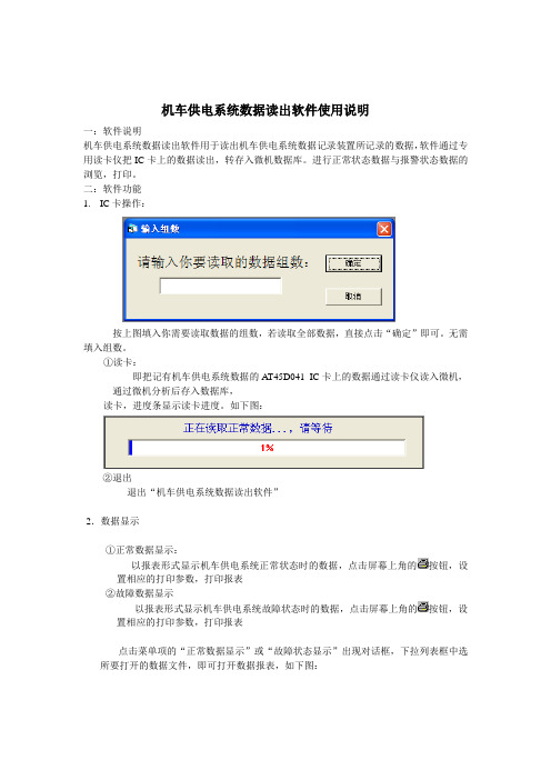
机车供电系统数据读出软件用于读出机车供电系统数据记录装置所记录的数据,软件通过专用读卡仪把IC卡上的数据读出,转存入微机数据库。
进行正常状态数据与报警状态数据的浏览,打印。
二:软件功能
1.IC卡操作:
按上图填入你需要读取数据的组数,若读取全部数据,直接点击“确定”即可。
无需填入组数。
①读卡:
即把记有机车供电系统数据的A T45D041 IC卡上的数据通过读卡仪读入微机,通过微机分析后存入数据库,
读卡,进度条显示读卡进度。
如下图:
②退出
退出“机车供电系统数据读出软件”
2.数据显示
①正常数据显示:
以报表形式显示机车供电系统正常状态时的数据,点击屏幕上角的按钮,设置相应的打印参数,打印报表
②故障数据显示
以报表形式显示机车供电系统故障状态时的数据,点击屏幕上角的按钮,设置相应的打印参数,打印报表
点击菜单项的“正常数据显示”或“故障状态显示”出现对话框,下拉列表框中选所要打开的数据文件,即可打开数据报表,如下图:
3. 注意事项:
1.读卡前,请注意读卡仪与计算机串口的正确连接。
2.把IC卡插入读卡仪时,注意IC卡芯片应朝下插入。
3.读卡器进行读写时,请不要拔卡,以避免烧坏卡片。
机车直流PWM调速系统打印版

摘要当今社会存在有多种形式的能量,例如核能、热能、势能、风能、化学能、太阳能等。
但可以直接或作为载体被人们在生产、生活使用的能量大多数是电能,而电机可以把电能转化为动能或把其它形式能量转化为电能。
电机对于科学技术的发展,改变社会的生产面貌,推动人类社会向前发展,具有极其重要的意义。
本论文设计的直流电机控制方法是利用单片机和脉宽调制控制技术(简称为 PWM)实现对直流电机的转速调节、正转、反转及停车控制。
采用了这种新型的 PWM 控制方法有其独特的优异性,具体来说主要有以下几点:(1)电路结构简单,需要的功率组件很少,这里只利用 AT89S52 单片机和模数转换器 ADC0832 及 1602LCD 模块组,大大节省了工程成本。
(2)开关频率高,电流容易连续,谐波少,电机损耗和发热都较小。
(3)低速性能好,调速范围宽。
(4)快速响应性能好,动态抗干扰能力强,当电动机的负载发生变化时,控制部分能够快速调整输出 PWM 信号的占空比,使得电动机维持在既定的转速上。
(5)主电路组件工作在开关状态,导通损耗小,装置效率高。
(6)控制简便,只要通过键盘输入想要的转速,系统自动改变控制 PWM 信号占空比的参数就能实现对直流电机的转速设置,使其在理论上能够稳定在任意速度工作。
关键词:单片机模数转换器 PWM目录1 概述 (1)1.1 选题背景 (1)1.2设计内容 (1)2 单闭环控制直流脉宽调速系统 (3)2.1 直流电机的PWM调速原理 (3)2.2 调速系统的静态指标 (5)2.3 PWM下直流电机的运行状态 (6)2.4 PWM变换器的类型 (6)3 PWM调速控制系统硬件设计 (8)3.1 AT89S52单片机简介 (8)3.1.1 引脚排列及功能AT89C52 (9)3.1.2 I/O 口线 (9)3.1.3 FLASH 编程的串行模式 (11)3.2 主电路设计PWM (12)3.3 MOSFET驱动电路设计 (14)3.4 A/D转换器 (15)3.5 Flash存储器 (16)3.6 Cs6839霍尔线形集成传感器 (19)3.7 I/O口串行扩展芯片 (20)3.8 键盘 (21)3.9 R-S触发器防抖电路 (23)3.10 硬件电路设计特点 (24)4 PWM调速控制系统软件设计 (26)4.1 主程序 (26)4.2 转速调节子程序 (26)4.3 ADC0832的模数转换子程序 (28)4.4 Flash存储器 (30)4.5 键盘与PCF8574 (33)4.6 遇障碍功能子程序 (35)结论 (37)参考文献 (38)1 概述1.1 选题背景近年来,直流电动机的结构和控制方式都发生了很大的变化。
IC卡技术知识
IC卡的基础知识:1、非接触卡:(1)ID卡:4100、4001、EM4102(瑞士产原装),频率为125Khz,又称低频只读卡。
没有存储空间,不能写入数据。
4001中料厚度0.65-0.7mm,常用0.7mm ,成品印刷卡面料厚度0.125,卡片压光可以做到0.95-1.0 mm加膜1、03mm。
白卡面料可用0.1mm,成卡厚度为0.9mm左右。
ID卡每张都有一个出厂初始代码,称为ID内码,此内码是一组10位16进制数,一般来讲我们的读卡机只用后面8位(即所谓的8H码,后8位的16进制数),通常讲的8H-10D是指把后8位的H(十六进制)码转换成10位的十进制码来使用,有的机具是用十六进制的后6位转换码来用(即6H-10D码表示为后6位的十六进制数转换为10位的十进制数),还有客户是用韦根26码、韦根34码等,如客户要求打印内码,生产下单一定要与客户沟通好。
通俗地讲,当ID芯片10进制内码<0016777215时的ABA码,6H、8H都是一样的,>0016777215时的内码6H、8H码不同,但6H一般是8位,若客户需要打10位码,打码时在前面加2个0即可。
一般白卡客户通俗要求打18位内码,此码实际是ABA8H-10D码(10位)+韦根26码(8位)的组合,客户实际只会使用其中一个码。
(关于有些ID卡片在不同机具上不通用的技术解释中有更进一步解释,可查看或传给客户看)ID卡国际内码常见知识:ID卡的曼彻斯特内码(10位十六进制码)=版本代码(第一位,H9)+客户代码(第二位,H8)+ID代码(第三位至第十位,H7、H6、H5、H4、H3、H2、H1、H0)例:10位内码125533FFFF表示版本代码为“1”,客户代码为“2”,ID代码(通常为8个数字、字母或组合)“5533FFFF”H9、H8、H7、H6、H5、H4、H3、H2、H1、H01 2 5 5 3 3 F F F F注:十六进制简称“H”,十进制简称“D”10H-13D[ABA(10H)]:H9-H0即10位的十六进制码“125533FFFF”换算为13位的十进制码为“007 87388 82559”08H-10D[ABA(8H)]:H7-H0即后8位十六进制码“5533FFFF”换算为10位的十进制码为“14294 71231”06H-08D[ABA(6H)]:H5-H0即后6位十六进制码“33FFFF”换算为8位十进制码为“034 07871”[如要求为06H-10D则表示后6位十六进制码“33FFFF”换算为10位十进制码为“00”+“034 07871”(即在8位前加两个0补齐)]韦根34[WG34(4H+4H)]:表示H7-H0后8位分前后两段各4个十六进制码分别换算为两组5位的十进制码用“,”分开组合,即H7-H4“5533”换算为“21811”,H3-H0“FFFF”换算为“65535”,最终显示结果为“21811,65535”韦根26码[WG26(2H+4H)]:表示H5-H0后6位十六进制码分前后两段2个、4个十六进制码分别换算为两组3位、5位的十进制码用“,”分开组合,即H5-H4“33”换算为“051”,H3-H0“FFFF”换算为“65535”,最终显示为“051,65535”。
AT45DB041D驱动第一部分(测试可用)
//AT_WP---片选信号---功能选择为GPIO PINSEL1 &=0xFF3FFFFF;
的[23...22]位! FIO1DIR |=WP;
//AT45DB041D保护信号P1.27---PINSEL1 //方向设置为输出引脚.
/**********************************/
***/
/*描述:从BUFFER中的指定地址开始读出指定长度的数据,
*/
/* 读到最后从buffer的开头重读.
*/
/*参数:
*/
/* buffer - 选择BUFFER,01H选择BUFFER 1,02H选择BUFFER 2
*/
/*
在该指令序列中,操作码D4H选择BUFFER 1,D6H选择BUFFER 2
)
//AT45DB041D保护信号
/*******************************************************/
/*初始化---保护,复位
*/
/*******************************************************/
void AT45DB_init(void)
***/
void AT45DB_BufferRead(uchar buffer,uchar BFA,uchar *pHeader,uint len)
{
uint i;
uchar busy=0;
//忙标致位busy---1:为不忙 0:为忙.
for(i=0;i<50000;i++) //等待不忙再操作--状态寄存器bit7:1为不忙,0为忙. 用for不用while防止死循环.
AT45DB014D中文说明

翻译:王兵洋
2017-7-10
1
1、大致描述
AT45DB041D 是 2.5V/2.7V 串行 FLASH 存储器,能够存储声音、图片、编程代码等大容量数据。它支持高速串行接 口,适用于要求高速数据操作的应用。它的 SPI 接口速率提高到了 66 MHz,4,325,376 bits 的数据由 2048 页(每页 256/264 bytes)数据组成。缓冲区允许在主存正在被重写的过程中接收(连续)数据,自带的读—修改—写控制单元能让修改 EEPROM 的冲突很方便的受到控制。有别于传统的 FLASH 存储器使用众多的功能线、地址线来存取数据, AT45DB041D 采用了快速串行接口来实现数据存取,明显的减少了管脚数目和方便了硬件制板,增加了系统可靠性, 减少了开关噪声,并且缩小了封装尺寸。能够在高密度、低管脚数、低压和低功耗的商业和工业应用中得到最优化的 发挥。 AT45DB041D 不需要很高的编程电压,只需要 2.7/2.5V——3.6V 单供电即可完成在编程操作。AT45DB041D 由 CS 引 脚来使能,芯片的数据操作由三线(SI、SO、SCK)组成的接口即可完成。 另外它的所有编程和擦除周期都是自同步的。
翻译:王兵洋
2017-7-10
3
5、芯片操作
芯片的各操作指令都是由主处理器发出,Table15-1 到 Table15-7 是操作代码的列表。一个有效的命令是 在 CS 有效,并且要紧随有效的 8 位操作码和合适的缓存或者主存中的地址。所有的串行操作都是高位 在前(MSB)。 标准的缓存区(264 bytes)是由 BFA8——BFA0 这 9 位地址数据来描述。主存地址是由 PA8——PA0 和 BA8——BA0 来指定,其中 PA8——PA0 这 9 位用来指定页地址,而 BA8——BA0 是这 9 位用来指 定页内数据存放的地址。 二进制页大小(256 bytes),缓存区的地址是由传统的 BFA7——BFA0 这 8 位来指定地址,主存中的地 址是由 A16——A0 来指定,其中 A16——A8 这 9 位用来指定页地址,而 A7——A0 是这 8 位用来指定 页内数据存放的地址。
串行快闪存储器AT45D041及其应用
串行快闪存储器AT45D041及其应用AT45D041是一由单5V供电、带串行接口的快闪存储器,该芯片特别适合于在系统反复编程,其4兆位的存储容量被分为2048页,每页264个字节。
除了主存储页外,AT45D041还包含2个SRAM数据缓冲区,每个区的容量均为264个字节,当主存储页正在编程时,缓冲区可接收外部数据。
传统快闪存储器往往利用多条地址线和并行接口来实现随机存取数据,而AT45D041则利用串行接口来实现连续存取数据。
简单的串行接口简化了硬件电路,使线路板尺寸变小,成本降低,抗干扰能力增强,系统的可靠性得以提高。
数据编程写入时,不需要高编程输入电压,只需要单5V(范围为4.5~5.5V)即可完成数据的写入及读出。
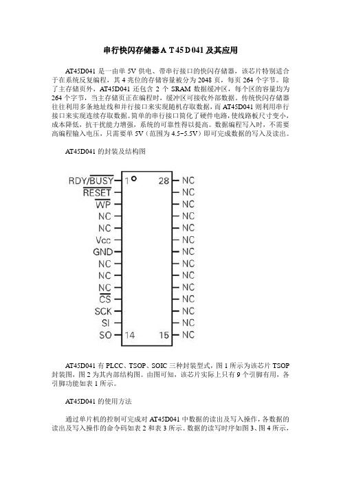
AT45D041的封装及结构图AT45D041有PLCC、TSOP、SOIC三种封装型式,图1所示为该芯片TSOP 封装图,图2为其内部结构图。
由图可知,该芯片实际上只有9个引脚有用,各引脚功能如表1所示。
AT45D041的使用方法通过单片机的控制可完成对AT45D041中数据的读出及写入操作,各数据的读出及写入操作的命令码如表2和表3所示。
数据的读写时序如图3、图4所示,由图可知,当芯片使能脚为低电平时,在时钟输入脚(SCK)的控制下,通过串行数据输入脚(SI),便可将命令码、主存储页或缓冲区地址码串行输入给该芯片,然后即可读或写入数据。
需注意的是,所有的命令码、地址、数据串行输入时,均是高位在前,低位在后。
下面具体介绍数据的读写方法。
数据的读出数据的读出包括主存储页直接读出、从主存储页读取数据至缓冲区、从缓冲区读数据、读状态寄存器等四种,除命令码不同外,读取的方法均大同小异,参见图3所示时序波形图,下面只介绍主存储页直接读取数据的方法。
主存储页读允许用户从2048主存储页的任一页中读取数据,如表2所示,在SCK时钟脉冲的控制下,先串行输入命令码(52H)、紧接着是4个保留位、然后是20个地址位(即11个页地址位和9个页中数据起始地址位)、最后是32个无关位。
IC卡技术知识

IC卡的基础知识:1、非接触卡:(1)ID卡:4100、4001、EM4102(瑞士产原装),频率为125Khz,又称低频只读卡。
没有存储空间,不能写入数据。
4001中料厚度0.65-0.7mm,常用0.7mm ,成品印刷卡面料厚度0.125,卡片压光可以做到0.95-1.0 mm加膜1、03mm。
白卡面料可用0.1mm,成卡厚度为0.9mm左右。
ID卡每张都有一个出厂初始代码,称为ID内码,此内码是一组10位16进制数,一般来讲我们的读卡机只用后面8位(即所谓的8H码,后8位的16进制数),通常讲的8H-10D是指把后8位的H(十六进制)码转换成10位的十进制码来使用,有的机具是用十六进制的后6位转换码来用(即6H-10D码表示为后6位的十六进制数转换为10位的十进制数),还有客户是用韦根26码、韦根34码等,如客户要求打印内码,生产下单一定要与客户沟通好。
通俗地讲,当ID芯片10进制内码<0016777215时的ABA码,6H、8H都是一样的,>0016777215时的内码6H、8H码不同,但6H一般是8位,若客户需要打10位码,打码时在前面加2个0即可。
一般白卡客户通俗要求打18位内码,此码实际是ABA8H-10D码(10位)+韦根26码(8位)的组合,客户实际只会使用其中一个码。
(关于有些ID卡片在不同机具上不通用的技术解释中有更进一步解释,可查看或传给客户看)ID卡国际内码常见知识:ID卡的曼彻斯特内码(10位十六进制码)=版本代码(第一位,H9)+客户代码(第二位,H8)+ID代码(第三位至第十位,H7、H6、H5、H4、H3、H2、H1、H0)例:10位内码125533FFFF表示版本代码为“1”,客户代码为“2”,ID代码(通常为8个数字、字母或组合)“5533FFFF”H9、H8、H7、H6、H5、H4、H3、H2、H1、H01 2 5 5 3 3 F F F F注:十六进制简称“H”,十进制简称“D”10H-13D[ABA(10H)]:H9-H0即10位的十六进制码“125533FFFF”换算为13位的十进制码为“007 87388 82559”08H-10D[ABA(8H)]:H7-H0即后8位十六进制码“5533FFFF”换算为10位的十进制码为“14294 71231”06H-08D[ABA(6H)]:H5-H0即后6位十六进制码“33FFFF”换算为8位十进制码为“034 07871”[如要求为06H-10D则表示后6位十六进制码“33FFFF”换算为10位十进制码为“00”+“034 07871”(即在8位前加两个0补齐)]韦根34[WG34(4H+4H)]:表示H7-H0后8位分前后两段各4个十六进制码分别换算为两组5位的十进制码用“,”分开组合,即H7-H4“5533”换算为“21811”,H3-H0“FFFF”换算为“65535”,最终显示结果为“21811,65535”韦根26码[WG26(2H+4H)]:表示H5-H0后6位十六进制码分前后两段2个、4个十六进制码分别换算为两组3位、5位的十进制码用“,”分开组合,即H5-H4“33”换算为“051”,H3-H0“FFFF”换算为“65535”,最终显示为“051,65535”。
酒店门锁介绍
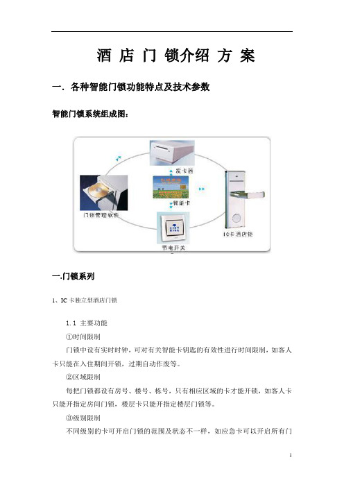
酒店门锁介绍方案一.各种智能门锁功能特点及技术参数智能门锁系统组成图:一.门锁系列1、IC卡独立型酒店门锁1.1 主要功能①时间限制门锁中设有实时时钟,可对有关智能卡钥匙的有效性进行时间限制,如客人卡只能在入住期间开锁,过期自动作废等。
②区域限制每把门锁都设有房号、楼号、栋号,只有相应区域的卡才能开锁,如客人卡只能开指定房间门锁,楼层卡只能开指定楼层门锁等。
③级别限制不同级别的卡可开启门锁的范围及状态不一样,如应急卡可以开启所有门锁,并且可开反锁,而客人卡只能开某个房间门锁,且不能开反锁。
④开锁记录每次开锁时,门锁都记录开锁卡号和时间,可保存最新300条记录,该记录可以通过数据卡采集。
根据特殊需要,可以定制存储700条或更多记录。
⑤挂失功能当出现钥匙卡丢失时,重新发一张新客人卡即可将丢失卡作废。
⑥应急功能当出现紧急状态时,可用应急卡将门锁置于常开状态,以便于人员和财物的疏散。
⑦封闭门锁功能根据需要,可封闭某个房间,使该房间所有钥匙卡失效(应急卡除外)。
⑧设置公共门功能根据需要,可设置楼层公共门(允许本楼层所有有效开门卡开启)和楼栋公共门(允许本楼栋所有有效开门卡开启)。
⑨可扩充功能智能卡容量大,除了可以存放门锁钥匙所需信息外,还可储存金额、保险箱密码等其他信息,因此客人凭一张卡,既可开锁,也可开保险箱、付费,可方便地实现一卡多用。
1.2 卡片类型1.2.1开门卡具备开门功能。
①应急卡:可在应急状态下开启系统内所有门锁,即使门锁反锁时也能开启。
由应急卡开启门锁时,门锁一直保持开启状态,直至插入任何其它合法开门卡为止。
应急卡一般由保安部或消防部门保管。
②总控卡:可以开启系统内所有门锁,总控卡一般由酒店总经理持有。
③楼栋卡:可以开启某栋楼的所有门锁,受时间限制,当门锁反锁时不能开启,楼栋卡一般由楼栋经理或其他相应人员保管使用。
④楼层卡:可以开启某个楼层的所有门锁,当门锁反锁时不能开启,楼层卡一般由楼层服务员或其他相应人员保管使用。
AT45DB041中文资料
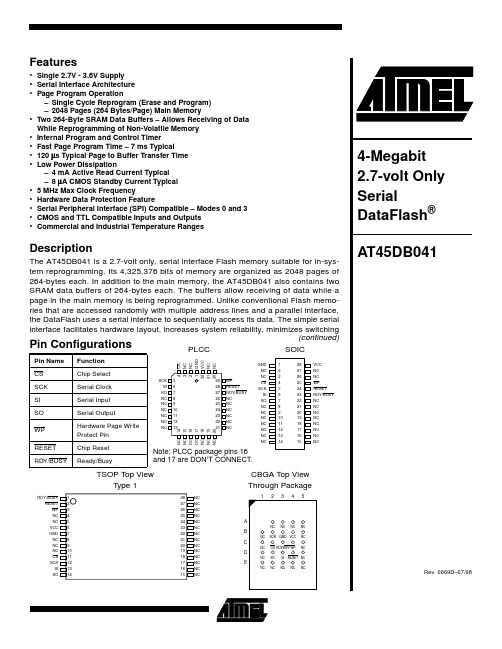
Features•Single 2.7V - 3.6V Supply •Serial Interface Architecture •Page Program Operation –Single Cycle Reprogram (Erase and Program)–2048 Pages (264 Bytes/Page) Main Memory•Two 264-Byte SRAM Data Buffers – Allows Receiving of Data While Reprogramming of Non-Volatile Memory •Internal Program and Control Timer •Fast Page Program Time – 7 ms Typical•120 µs Typical Page to Buffer Transfer Time •Low Power Dissipation–4 mA Active Read Current Typical –8 µA CMOS Standby Current Typical • 5 MHz Max Clock Frequency•Hardware Data Protection Feature•Serial Peripheral Interface (SPI) Compatible – Modes 0 and 3•CMOS and TTL Compatible Inputs and Outputs •Commercial and Industrial Temperature RangesDescriptionThe AT45DB041 is a 2.7-volt only, serial interface Flash memory suitable for in-sys-tem reprogramming. Its 4,325,376 bits of memory are organized as 2048 pages of 264-bytes each. In addition to the main memory, the AT45DB041 also contains two SRAM data buffers of 264-bytes each. The buffers allow receiving of data while a page in the main memory is being reprogrammed. Unlike conventional Flash memo-ries that are accessed randomly with multiple address lines and a parallel interface,the DataFlash uses a serial interface to sequentially access its data. The simple serial interface facilitates hardware layout, increases system reliability, minimizes switchingPin Configurations Pin Name Function CS Chip Select SCK Serial Clock SI Serial Input SO Serial Output WP Hardware Page Write Protect Pin RESET Chip Reset RDY/BUSYReady/BusyTSOP T op ViewT ype 1CBGA T op View Through Package(continued)and 17 are DON’T CONNECT .noise, and reduces package size and active pin count. The device is optimized for use in many commercial and indus-trial applications where high density, low pin count, low voltage, and low power are essential. Typical applications for the DataFlash are digital voice storage, image storage, and data storage. The device operates at clock frequencies up to 5 MHz with a typical active read current consumption of 4 mA.To allow for simple in-system reprogrammability, the AT45DB041 does not require high input voltages for pro-gramming. The device operates from a single power sup-ply, 2.7V to 3.6V, for both the program and read operations. The AT45DB041 is enabled through the chip consisting of the Serial Input (SI), Serial Output (SO), and the Serial Clock (SCK).All programming cycles are self-timed, and no separate erase cycle is required before programming.Block Diagram Device OperationThe device operation is controlled by instructions from the host processor. The list of instructions and their associated opcodes are contained in Table 1 and Table 2. A valid instruction starts with the falling edge of CS followed by the appropriate 8-bit opcode and the desired buffer or main memory address location. While the CS pin is low, toggling the SCK pin controls the loading of the opcode and the desired buffer or main memory address location through the SI (serial input) pin. All instructions, addresses, and data are transferred with the most significant bit (MSB) first. ReadBy specifying the appropriate opcode, data can be read from the main memory or from either one of the two data buffers.MAIN MEMORY P AGE READ: A main memory read allows the user to read data directly from any one of the 2048 pages in the main memory, bypassing both of the data buff-ers and leaving the contents of the buffers unchanged. To start a page read, the 8-bit opcode, 52H, is followed by 24 address bits and 32 don’t care bits. In the AT45DB041, the first four address bits are reserved for larger density devices (see Notes on page8), the next 11 address bits (PA10-PA0) specify the page address, and the next nine address bits (BA8-BA0) specify the starting byte address within the page. The 32 don’t care bits which follow the 24 address bits are sent to initialize the read operation. Fol-lowing the 32 don’t care bits, additional pulses on SCK result in serial data being output on the SO (serial output) pin. The CS pin must remain low during the loading of the opcode, the address bits, and the reading of data. When the end of a page in main memory is reached during a main memory page read, the device will continue reading at the beginning of the same page. A low to high transition on the CS pin will terminate the read operation and tri-state the SO pin.BUFFER READ: Data can be read from either one of the two buffers, using different opcodes to specify which buffer to read from. An opcode of 54H is used to read data from buffer 1, and an opcode of 56H is used to read data from buffer 2. To perform a buffer read, the eight bits of the opcode must be followed by 15 don’t care bits, nine address bits, and eight don't care bits. Since the buffer size is 264-bytes, nine address bits (BFA8-BFA0) are required to specify the first byte of data to be read from the buffer.AT45DB041opcode, the address bits, the don’t care bits, and the read-ing of data. When the end of a buffer is reached, the device will continue reading back at the beginning of the buffer. A low to high transition on the CS pin will terminate the read operation and tri-state the SO pin.MAIN MEMORY PAGE TO BUFFER TRANSFER: A page of data can be transferred from the main memory to either buffer 1 or buffer 2. An 8-bit opcode, 53H for buffer 1 and 55H for buffer 2, is followed by the four reserved bits, 11 address bits (PA10-PA0) which specify the page in main memory that is to be transferred, and nine don’t care bits. The CS pin must be low while toggling the SCK pin to load the opcode, the address bits, and the don’t care bits from the SI pin. The transfer of the page of data from the main memory to the buffer will begin when the CS pin transitions from a low to a high state. During the transfer of a page of data (t XFR), the status register can be read to determine whether the transfer has been completed or not.MAIN MEMORY P AGE TO BUFFER COMPARE: A page of data in main memory can be compared to the data in buffer 1 or buffer 2. An 8-bit opcode, 60H for buffer 1 and 61H for buffer 2, is followed by 24 address bits consisting of the four reserved bits, 11 address bits (PA10-PA0) which spec-ify the page in the main memory that is to be compared to the buffer, and nine don't care bits. The loading of the opcode and the address bits is the same as described pre-viously. The CS pin must be low while toggling the SCK pin to load the opcode, the address bits, and the don't care bits the 264 bytes in the selected main memory page will be compared with the 264 bytes in buffer 1 or buffer 2. During this time (t XFR), the status register will indicate that the part is busy. On completion of the compare operation, bit 6 of the status register is updated with the result of the com-pare.ProgramBUFFER WRITE: Data can be shifted in from the SI pin into either buffer 1 or buffer 2. To load data into either buffer, an 8-bit opcode, 84H for buffer 1 or 87H for buffer 2, is followed by 15 don't care bits and nine address bits (BFA8-BFA0). The nine address bits specify the first byte in the buffer to be written. The data is entered following the address bits. If the end of the data buffer is reached, the device will wrap around back to the beginning of the buffer. Data will continue to be loaded into the buffer until a low to BUFFER TO MAIN MEMORY PAGE PROGRAM WITH BUILT-IN ERASE: Data written into either buffer 1 or buffer 2 can be programmed into the main memory. An 8-bit opcode, 83H for buffer 1 or 86H for buffer 2, is followed by the four reserved bits, 11 address bits (PA10-PA0) that specify the page in the main memory to be written, and nine additional don't care bits. When a low to high transition occurs on the CS pin, the part will first erase the selected page in main memory to all 1s and then program the data stored in the buffer into the specified page in the main memory. Both the erase and the programming of the page are internally self timed and should take place in a maxi-mum time of t EP. During this time, the status register will indicate that the part is busy.BUFFER TO MAIN MEMORY PAGE PROGRAM WITH-OUT BUILT-IN ERASE: A previously erased page within main memory can be programmed with the contents of either buffer 1 or buffer 2. An 8-bit opcode, 88H for buffer 1 or 89H for buffer 2, is followed by the four reserved bits, 11 address bits (PA10-PA0) that specify the page in the main memory to be written, and nine additional don’t care bits. When a low to high transition occurs on the CS pin, the part will program the data stored in the buffer into the specified page in the main memory. It is necessary that the page in main memory that is being programmed has been previ-ously programmed to all 1s (erased state). The program-ming of the page is internally self timed and should take place in a maximum time of t P. During this time, the status register will indicate that the part is busy.MAIN MEMORY PAGE PROGRAM: This operation is a combination of the Buffer Write and Buffer to Main Memory Page Program with Built-In Erase operations. Data is first shifted into buffer 1 or buffer 2 from the SI pin and then pro-grammed into a specified page in the main memory. An 8-bit opcode, 82H for buffer 1 or 85H for buffer 2, is followed by the four reserved bits and 20 address bits. The 11 most significant address bits (PA10-PA0) select the page in the main memory where data is to be written, and the next nine address bits (BFA8-BFA0) select the first byte in the buffer to be written. After all address bits are shifted in, the part will take data from the SI pin and store it in one of the data buffers. If the end of the buffer is reached, the device will wrap around back to the beginning of the buffer. When there is a low to high transition on the CS pin, the part will first erase the selected page in main memory to all 1s and then program the data stored in the buffer into the specified page in the main memory. Both the erase and the program-ming of the page are internally self timed and should take place in a maximum of time t EP. During this time, the status register will indicate that the part is busy.AUTO P AGE REWRITE: This mode is only needed if multi-ple bytes within a page or multiple pages of data are modi-fied in a random fashion. This mode is a combination of two operations: Main Memory Page to Buffer Transfer and Buffer to Main Memory Page Program with Built-In Erase.A page of data is first transferred from the main memory to buffer 1 or buffer 2, and then the same data (from buffer 1 or buffer 2) is programmed back into its original page of main memory. An 8-bit opcode, 58H for buffer 1 or 59H for buffer 2, is followed by the four reserved bits, 11 address元器件交易网bits (PA10-PA0) that specify the page in main memory to be rewritten, and nine additional don't care bits. When a low to high transition occurs on the CS pin, the part will first transfer data from the page in main memory to a buffer and then program the data from the buffer back into same page of main memory. The operation is internally self-timed and should take place in a maximum time of t EP. During this time, the status register will indicate that the part is busy.If the main memory is programmed or reprogrammed sequentially page by page, then the programming algo-rithm shown in Figure 1 is recommended. Otherwise, if multiple bytes in a page or several pages are programmed randomly in the main memory, then the programming algo-rithm shown in Figure 2 is recommended.STATUS REGISTER: The status register can be used to determine the device’s ready/busy status, the result of a Main Memory Page to Buffer Compare operation, or the device density. To read the status register, an opcode of 57H must be loaded into the device. After the last bit of the opcode is shifted in, the eight bits of the status register, starting with the MSB (bit 7), will be shifted out on the SO pin during the next eight clock cycles. The five most-signifi-cant bits of the status register will contain device informa-tion, while the remaining three least-significant bits are reserved for future use and will have undefined values. After bit 0 of the status register has been shifted out, the SCK is being toggled) starting again with bit 7. The data in the status register is constantly updated, so each repeating sequence will output new data.Ready/busy status is indicated using bit 7 of the status reg-ister. If bit 7 is a 1, then the device is not busy and is ready to accept the next command. If bit 7 is a 0, then the device is in a busy state. The user can continuously poll bit 7 of the status register by stopping SCK once bit 7 has been output. The status of bit 7 will continue to be output on the SO pin, and once the device is no longer busy, the state of SO will change from 0 to 1. There are six operations which can cause the device to be in a busy state: Main Memory Page to Buffer Transfer, Main Memory Page to Buffer Compare, Buffer to Main Memory Page Program with Built-In Erase, Buffer to Main Memory Page Program without Built-In Erase, Main Memory Page Program, and Auto Page Rewrite.The result of the most recent Main Memory Page to Buffer Compare operation is indicated using bit 6 of the status register. If bit 6 is a 0, then the data in the main memory page matches the data in the buffer. If bit 6 is a 1, then at least one bit of the data in the main memory page does not match the data in the buffer.The device density is indicated using bits 5, 4, and 3 of the status register. For the AT45DB041, the three bits are 0, 1, and 1. The decimal value of these three binary bits does not equate to the device density; the three bits represent a combinational code relating to differing densities of Serial DataFlash devices, allowing a total of eight different density configurations.Read/Program Mode SummaryThe modes listed above can be separated into two groups — modes which make use of the flash memory array (Group A) and modes which do not make use of the flash memory array (Group B).Group A modes consist of:1.Main memory page read2.Main memory page to buffer 1 (or 2) transfer3.Main memory page to buffer 1 (or 2) compare4.Buffer 1 (or 2) to main memory page program withbuilt-in erase5.Buffer 1 (or 2) to main memory page program with-out built-in erase6.Main memory page program7.Auto page rewriteGroup B modes consist of:1.Buffer 1 (or 2) read2.Buffer 1 (or 2) write3.Status readIf a Group A mode is in progress (not fully completed) then another mode in Group A should not be started. However, during this time in which a Group A mode is in progress, modes in Group B can be started.This gives the Serial DataFlash the ability to virtually accommodate a continuous data stream. While data is being programmed into main memory from buffer 1, data can be loaded into buffer 2 (or vice versa). See application note AN-4 (“Using Atmel’s Serial DataFlash”) for more details.HARDWARE PAGE WRITE PROTECT:held low, the first 256 pages of the main memory cannot be reprogrammed. The only way to reprogram the first 256 pages is to first drive the protect pin high and then use the program commands previously mentioned.Status Register FormatBit 7Bit 6Bit 5Bit 4Bit 3Bit 2Bit 1Bit 0 RDY/BUSY COMP011X X X 元器件交易网AT45DB041the operation in progress and reset the internal state machine to an idle state. The device will remain in the reset pin. Normal operation can resume once the RESET pin is brought back to a high level.The device also incorporates an internal power-on reset pin during power-on sequences.READY/BUSY: This open drain output pin will be driven low when the device is busy in an internally self-timed oper-ation. This pin, which is normally in a high state (through an external pull-up resistor), will be pulled low during program-ming operations, compare operations, and during page-to-buffer transfers.The busy status indicates that the Flash memory array and one of the buffers cannot be accessed; read and write operations to the other buffer can still be performed.Power On/Reset StateWhen power is first applied to the device, or when recover-ing from a reset condition, the device will default to SPI mode 3. In addition, the SO pin will be in a high impedance required to start a valid instruction. The SPI mode will be automatically selected on every falling edge of CS by sam-pling the inactive clock state.Note:1.After power is applied and V CC is at the minimum specified data sheet value, the system should wait 20 ms before an oper-ational mode is started.Absolute Maximum Ratings*T emperature Under Bias................................-55°C to +125°C *NOTICE:Stresses beyond those listed under “Absolute Maximum Ratings” may cause permanent dam-age to the device. This is a stress rating only and functional operation of the device at these or any other conditions beyond those indicated in the operational sections of this specification is not implied. Exposure to absolute maximum rating conditions for extended periods may affect device reliability.Storage T emperature.....................................-65°C to +150°C All Input Voltages (including NC Pins)with Respect to Ground...................................-0.6V to +6.25V All Output Voltageswith Respect to Ground.............................-0.6V to V CC + 0.6VDC and AC Operating RangeAT45DB041Operating T emperature (Case)Com.0°C to 70°C Ind.-40°C to 85°C V CC Power Supply (1)2.7V to3.6V元器件交易网DC CharacteristicsSymbol Parameter ConditionMinTyp Max Units I SB Standby Current CS, RESET , WP = V IH , all inputs at CMOS levels820µA I CC1Active Current, Read Operationf = 5 MHz; I OUT = 0 mA; V CC = 3.6V 410mA I CC2Active Current,Program/Erase Operation V CC = 3.6V 1535mA I LI Input Load Current V IN = CMOS levels 1µA I LO Output Leakage Current V I/O = CMOS levels1µA V IL Input Low Voltage 0.6V V IH Input High Voltage 2.0V V OL Output Low Voltage I OL = 1.6 mA; V CC = 2.7V 0.4V V OHOutput High VoltageI OH = -100 µAV CC - 0.2VVAC CharacteristicsSymbol Parameter MinTypMax Units f SCK SCK Frequency 5MHz t WH SCK High Time 80ns t WL SCK Low Time 80nst CS Minimum CS High Time 350nst CSS CS Setup Time 350ns t CSH CS Hold Time350ns t CSB CS High to RDY/BUSY Low 200ns t SU Data In Setup Time 15ns t H Data In Hold Time 35ns t HO Output Hold Time 0ns t DIS Output Disable Time 100ns t V Output Valid120ns t XFR Page to Buffer T ransfer/Compare Time 120250µs t EP Page Erase and Programming Time 1020ms t P Page Programming Time 714ms t RST RESET Pulse Width 10µs t RECRESET Recovery Time1µsInput Test Waveforms and Measurement Levelst R , t F < 20 ns (10% to 90%)Output Test Load元器件交易网AT45DB041 AC WaveformsTwo different timing diagrams are shown below. Waveform 1 shows the SCK signal being low when CS makes a high-to-low transition, and Waveform 2 shows the SCK signal being high when CS makes a high-to-low transition. Both waveforms show valid timing diagrams. The setup and hold times for the SI signal are referenced to the low-to-high transition on the SCK signal.Waveform 1 shows timing that is also compatible with SPI Mode 0, and Waveform 2 shows timing that is compatible with SPI Mode 3.Waveform 1 - Inactive Clock Polarity LowWaveform 2 - Inactive Clock Polarity High元器件交易网Reset Timing (Inactive Clock Polarity Low Shown)Command Sequence for Read/Write Operations (Except Status Register Read)Notes: 1.“r” designates bits reserved for larger densities.2.It is recommended that “r” be a logical “0” for densities of 4M bit or smaller.3.For densities larger than 4M bit, the “r” bits become the most significant Page Address bit for the appropriate density.元器件交易网AT45DB041Write OperationsThe following block diagram and waveforms illustrate the various write sequences available.Main Memory Page Program through BuffersBuffer WriteBuffer to Main Memory Page Program(Data from Buffer Programmed into Flash Page)n = 1st byte read n+1 = 2nd byte read元器件交易网Read OperationsThe following block diagram and waveforms illustrate the various read sequences available.Main Memory Page ReadMain Memory Page to Buffer Transfer (Data from Flash Page Read into Buffer)Buffer Readn = 1st byte written n+1 = 2nd byte written元器件交易网Main Memory Page ReadBuffer ReadStatus Register ReadMain Memory Page ReadBuffer ReadStatus Register ReadMain Memory Page ReadBuffer 1 Read Buffer 2 Read Main Memory Page to Buffer 1TransferMain Memory Page to Buffer 2TransferMain Memory Page to Buffer 1CompareMain Memory Page to Buffer 2CompareBuffer 1 WriteBuffer 2 WriteOpcode 52H 54H 56H 53H 55H 60H 61H 84H 87H 000000011111111100000001100111110000000000000011010011101100001000110101r X X r r r r X X r X X r r r r X X r X X r r r r X X r X X r r r r X X P A10X X P A10P A10P A10P A10X X P A9X X P A9P A9P A9P A9X X P A8X X P A8P A8P A8P A8X X P A7X X P A7P A7P A7P A7X X P A6X X P A6P A6P A6P A6X X P A5X X P A5P A5P A5P A5X X P A4X X P A4P A4P A4P A4X X P A3X X P A3P A3P A3P A3X X P A2X X P A2P A2P A2P A2X X P A1X X P A1P A1P A1P A1X X P A0X X P A0P A0P A0P A0X X BA8BFA8BFA8X X X X BFA8BFA8BA7BFA7BFA7X X X X BFA7BFA7BA6BFA6BFA6X X X X BFA6BFA6BA5BFA5BFA5X X X X BFA5BFA5BA4BFA4BFA4X X X X BFA4BFA4BA3BFA3BFA3X X X X BFA3BFA3BA2BFA2BFA2X X X X BFA2BFA2BA1BFA1BFA1X X X X BFA1BFA1BA0BFA0BFA0XXXXBFA0BFA0X X X X (Don’t Care)r (reserved bits)X X X X X X X X X X X X X X X X X X X XX•••X (64th bit)X (Don’t Care)r (reserved bits)Buffer 1 to Main Memory Page Program with Built-InEraseBuffer 2 to Main Memory Page Program with Built-InEraseBuffer 1 to Main Memory Page Program without Built-In EraseBuffer 2 to Main Memory Page Program without Built-In EraseMain Memory Page Program Through Buffer 1Main Memory Page Program Through Buffer 2Auto Page Rewrite Through Buffer 1Auto Page Rewrite Through Buffer 2Status Register Opcode 83H 86H 88H 89H 82H 85H 58H 59H 57H 111111000000000111000000000000000111001100110010001001110010001100101011r r r r r r r r r r r r r r r r r r r r r r r r r r r r r r r r P A10P A10P A10P A10P A10P A10P A10P A10P A9P A9P A9P A9P A9P A9P A9P A9P A8P A8P A8P A8P A8P A8P A8P A8P A7P A7P A7P A7P A7P A7P A7P A7P A6P A6P A6P A6P A6P A6P A6P A6P A5P A5P A5P A5P A5P A5P A5P A5P A4P A4P A4P A4P A4P A4P A4P A4P A3P A3P A3P A3P A3P A3P A3P A3P A2P A2P A2P A2P A2P A2P A2P A2P A1P A1P A1P A1P A1P A1P A1P A1P A0P A0P A0P A0P A0P A0P A0P A0X X X X BA8BA8X X X X X X BA7BA7X X X X X X BA6BA6X X X X X X BA5BA5X X X X X X BA4BA4X X X X X X BA3BA3X X X X X X BA2BA2X X X X X X BA1BA1X X XXXXBA0BA0XXFigure 1. Algorithm for Programming or Reprogramming of the Entire Array SequentiallyNotes: 1.This type of algorithm is used for applications in which the entire array is programmed sequentially, filling the array page-by-page.2. A page can be written using either a Main Memory Page Program operation or a Buffer Write operation followed by a Bufferto Main Memory Page Program operation.3.The algorithm above shows the programming of a single page. The algorithm will be repeated sequentially for each pagewithin the entire array.Figure 2. Algorithm for Randomly Modifying DataNotes: 1.T o preserve data integrity, each page of the DataFlash memory array must be updated/rewritten at least once within every 10,000 cumulative page erase/program operations.2. A Page Address Pointer must be maintained to indicate which page is to be rewritten. The Auto Page Rewrite commandmust use the address specified by the Page Address Pointer.3.Other algorithms can be used to rewrite portions of the Flash array. Low power applications may choose to wait until 10,000cumulative page erase/program operations have accumulated before rewriting all pages of the Flash array. See application note AN-4 (“Using Atmel’s Serial DataFlash”) for more details.Ordering Informationf SCK (MHz)I CC (mA)Ordering Code Package Operation Range Active Standby5100.02A T45DB041-JCA T45DB041-RCA T45DB041-TCA T45DB041-CC 32J28R28T24C1Commercial(0°C to 70°C)5100.02A T45DB041-JIA T45DB041-RIA T45DB041-TIA T45DB041-CI32J28R28T24C1Industrial(-40°C to 85°C) Package Type32J32-Lead, Plastic J-Leaded Chip Carrier Package (PLCC)28R28-Lead, 0.330" Wide, Plastic Gull-Wing Small Outline Package (SOIC) 28T28-Lead, Plastic Thin Small Outline Package (TSOP)24C124-Ball, 5 x 5 Array Plastic Chip-Scale Ball Grid Array (CBGA)Packaging Information。
新型大容量闪存AT45DB041
新型大容量闪存AT45DB041AT45DB041: New High capability Flash Memory■北方交通大学现代通信研究所熊磊张鹏姚冬苹AT45DB041是A TMEL公司的新型FLASH芯片。
该芯片具有容量大、读写速度快、外围电路少等诸多优点,更为重要的是该芯片可最低工作在 2.5V,工作电流仅为4mA,因此在移动通信、便携等场合得到了广泛的应用。
芯片工作原理与硬件连接AT45DB041中的数据按页存放,主存共2048页,每页264字节,所以总容量为528K 字节(约4M比特)。
存放在主存中的数据掉电不丢失。
除了主存以外,AT45DB041还有两个容量为264字节的数据缓存。
缓存可以用作主存与外部进行数据交换时的缓冲区域,也可以暂存一些临时数据。
缓存读写方便迅速,但掉电数据会丢失。
AT45DB041数据读写采用串行方式,读写速度快,从页到缓存的传输时间为80 s 左右,并且兼容CMOS和TTL输入和输出。
AT45DB041通过片选管脚/CS使能,通过串行输出(SO)和串行输入(SI)进行数据读和写。
由串行时钟(SCK)对读写进行控制。
设备运行受微处理器的指令控制。
一条有效的指令起始于/CS管脚的下降沿,并跟随相应的8位操作码和指定的缓存或主存地址码。
当/CS管脚为低时,轮换时钟管脚(SCK)控制操作码和指定的缓存或主存地址码通过SI口的载入。
所有的指令、地址和数据都从高字节开始传送。
数据读取读缓存:通过不同的操作码可选择读取两个缓存中的其中一个(操作码54H用作读缓存1,而操作码56H用作读缓存2)。
为了实现读缓存的操作,在8位操作码后必须跟有15位任意码,9位地址码和8位任意码。
其中9位地址码(BFA8-BFA0)被用作指定要读取的首字节。
在轮换时钟SCK的控制下,从SI载入操作码、地址码、任意码。
当载入结束后,在SCK轮换时钟的控制下,缓存中的数据就可以从SO读出。
- 1、下载文档前请自行甄别文档内容的完整性,平台不提供额外的编辑、内容补充、找答案等附加服务。
- 2、"仅部分预览"的文档,不可在线预览部分如存在完整性等问题,可反馈申请退款(可完整预览的文档不适用该条件!)。
- 3、如文档侵犯您的权益,请联系客服反馈,我们会尽快为您处理(人工客服工作时间:9:00-18:30)。
主内存页编程 此操作是缓存写入和带内置擦除的缓存至主内存页编程操作的组合 数据首先由 SI 引脚输入缓存 1
或缓存 2 然后写入主内存指定页 8 bit 操作码 82H 为缓存 1 或 85H 为缓存 2 后跟 4 bit 保留位和 20 bit 地址 最高 11 bit 地址 PA10-PA0 选择主内存中要写入数据的页 后 9 bit 地址 BFA8BFA0 选择缓存中要写的首字节 在所有的地址输入后 器件将从 SI 引脚取数据 存入一个缓存 如 果达到缓存终端 器件将返回缓存始端 当 CS 引脚上发生由低至高的跳变时 器件将首先擦除主内存 中所选的页 使其为全 1 然后将存储在缓存中的数据写入主内存中的指定页 页的擦除和写入均内 部自定时 并发生在最大时间 tEP 之内 在此时间 状态寄存器将指示器件忙
无内置擦除的缓存至主内存页编程 主内存中预先擦除的页可写入缓存 1 或缓存 2 的内容 8 bit 操作码 88H 为缓存 1 或 89H 为缓存
2 后跟 4 bit 保留位 11 bit 地址 PA10-PA0 指定主内存中要写入的页 和 9 bit 任意数据 当 CS 引 脚上发生由低至高的跳变时 器件将把缓存中存储的数据写入主内存中的指定页 必要条件是 主内存 中要写入的页预先已写为全 1 擦除状态 页的写入是内部自定时的 并发生在最大时间 tP 之 内 在此时间 状态寄存器将指示器件忙
以通过一旦输出了 bit 7 就停止 SCK 的方法连续截取状态寄存器的 bit 7 bit 7 的状态将在 SO 引脚上连续输出 一旦器件不再忙 SO 的状态将由 0 变为 1 有 6 种操作能够
使器件处于忙状态 主内存页转存至缓存 主内存页与缓存比较 带内置擦除的缓存至主内存页编程 不带内置擦除的缓存至主内存页编程 主内存页编程和自动页重写
当 CS 引脚出现由低至高的跳变时 器件将首先将数据从主内存页转存到缓存 然后将数据从缓存写 回主内存中原来的页 操作是自定时的 并在最大时间 tEP 内完成 在此时间内 状态寄存器将指示器 件忙
如果主内存是逐页连续编程的 则推荐图 1 所示的编程算法 否则 如果主内存中一页内的多字节 或多页随机编程 推荐图 2 中所示的算法
为 4 bit 保留位 11 bit 地址 PA10-PA0 指定主内存中要转存的页 和 9 bit 任意数据 在向 SCK 引脚输入时钟以通过 SI 引脚载入操作码 地址和无关位的同时 必须保持 CS 引脚为低
电平 当 CS 引脚从低至高跳变时 主内存数据页向缓存的转存将开始 在数据页转存期间 tXFR
自动页重写 此模式仅当以随机方式修改一页内的多个字节或多页数据时才需要 此模式是两种操作的组合 主
内存页至缓存转存和带内置擦除的缓存至主内存页编程 一页数据首先从主内存转存至缓存 1 或缓存 2 然后同样的数据 从缓存 1 或缓存 2 写回主内存中的原始页 8 位操作码 58H 为缓存 1 或 59 为缓存 2 后跟 4 个保留位 指明主内存中所重写页的 11 个地址位 PA10-PA0 9 个附加的无关位
北京卡来通电子技术有限公司
Beijing Card Reader Electronic Technique Co.,
AT45D041
第1页共1页
AT45D041 技术说明
特点
• 单一 4.5V - 5.5V 电源 • 串行接口 • 支持页编程操作
– 单一循环编程 擦除并编程 – 2048 页 264 字节/页 主内存 • 具有两个 264 字节 SRAM 数据缓存 • 具有内部编程和控制定时器 • 快速页编程 典型 7 ms • 页至缓存典型传输时间 80 µs • 低功耗 – 典型工作状态读取电流 15 mA – 典型 CMOS 待命状态电流 20 µA • 最高时钟频率 10 MHz • 具有硬件数据保护功能 • 兼容串行外设接口 Mode 0 和 3 • 兼容 CMOS 和 TTL 输入及输出 • 适应商业和工业温度范围
主内存页与缓存比较的当前结果由状态寄存器的 bit 6 指示 如果 bit 6 为 0 则主内存页中的数据与 缓存中的数据相符 如果 bit 6 为 1 则主内存中的数据至少有 1 位与缓存中的数据不符
器件的集成度由状态寄存器的 bits 5, 4 和 3 指示 对于 AT45D041 此 3 位是 0 1 和 1 这 3 个二 进制位的十进制值并不等于器件的集成度 这 3 位代表了与串行 DataFlash 不同集成度相关的组合码 共有 8 种不同的集成度结构
地址 北京海淀区知春路 108 号豪景大厦 C 座 601 室 100086 电话 010-62104383 010-82104384 传真 010-62104385
北京卡来通电子技术有限公司
Beijing Card Reader Electronic Technique Co.,
AT45D041
带内置擦除的缓存至主内存页编程
写入缓存 1 或缓存 2 的数据可以写至主内存 8 bit 操作码 83H 为缓存 1 或 86H 为缓存 2 后跟 4 bit 保留位 11 bit 地址 PA10-PA0 指定主内存中要写入的页 和 9 bit 任意数据 当 CS 引脚上发生 由低至高的跳变时 器件将首先擦除主内存中所选的页 使其为全 1 然后将存储在缓存中的数据写 入主内存中的指定页 页的擦除和写入均内部自定时 并发生在最大时间 tEP 之内 在此时间 状态寄 存器将指示器件忙
方框图
北京卡来通电子技术有限公司
Beijing Card Reader Electronic Technique Co.,
AT45D041
第2页共2页
页 264 字节
FLASH 存储器矩阵
缓冲器 264 字节
缓冲器 264 字节 I/O 接口
器件操作
器件操作受来自主机处理器的指令控制 指令表及其相关的操作码见表 1 和表 2 有效的指令起始于 CS 的下降沿 含 8 bit 操作码和缓存或主内存地址 当 CS 为低电平时 跳变的 SCK 引脚电平控制操作 码和缓存或主内存地址通过 SI 串行输入 脚输入 所有的指令 地址和数据传送都是最高位在前
允许在对非易失性存储器编程的同时接收数据
说明
AT45D041 是单一 5V 供电串行接口 Flash 存储卡 适用于系统内重复编程 它共有 4,325,376 bits 内存 组织为 2048 页 每页 264 字节 处主内存之外 AT45D041 还有两个 SRAM 数据缓存 每个 264 字节 缓存使得主内存的一页正在编程的同时可以接收数据 与用多条地址线和一个并行接口随机 访问的传统 Flash 存储器不同 其数据闪存 DataFlash 采用串行接口顺序访问数据 这种简单的串行接 口方便了硬件布局 增强了系统灵活性 减小了切换噪声 压缩了封装尺寸和有效引脚数量 此器件是 针对要求大容量 低引脚数 低电压和低功耗的许多工商业应用优化的 DataFlash 的典型应用有数字语 音存储 图像存储和数据存储 器件工作时钟高达 10 MHz 典型工作状态读取电流损耗为 15 mA
引脚定义
引脚名称 CS SCK SI SO WP RESET RDY/BUSY
功能 片选 串行时钟 串行输入 串行输出 硬件页写入保护 片复位 就绪/忙
地址 北京海淀区知春路 108 号豪景大厦 C 座 601 室 100086 电话 010-62104383 010-82104384 传真 010-62104385
第3页共3页
可以读取状态寄存器以确定转存是否完成
主内存与缓存比较
主内存中的数据页可与缓存 1 或缓存 2 中的数据比较 8 bit 操作码 60H 为缓存 1 61H 为缓存 2 其后为 24 bit 地址 由 4 bit 保留位 11 bit 地址 PA10-PA0 指定主内存中要比较的页 和 9 bit 任意 数据组成 操作码和地址位的载入同上 在向 SCK 引脚输入时钟以通过 SI 引脚载入操作码 地址和无 关位的同时 必须保持 CS 引脚为低电平 当 CS 引脚从低至高跳变时 所选主内存页的 264 字节数据 将与缓存 1 或缓存 2 中的 264 字节数据比较 此期间 tXFR 状态寄存器将指示器件是否忙 当比较 操作完成时 状态寄存器的 bit 6 被更新位比较结果
地址 北京海淀区知春路 108 号豪景大厦 C 座 601 室 100086 电话 010-62104383 010-82104384 传真 010-62104385
北京卡来通电子技术有限公司
Beijing Card Reader Electronic Technique Co.,
AT45D041
缓存读取 数据可以通过两个缓存之一来读取 使用不同的操作码可指定使用哪个缓存 操作码 54H 是从缓存
1 读取数据 而操作码 56H 是从缓存 2 读取数据 在缓存读取指令中 8 bit 操作码之后 有 15 bit 任意 数据 9 bit 地址以及 8 bit 任意数据 因为缓存大小是 264 字节 需要 9 bit 地址 BFA8-BFA0 来指定 从缓存读取的首字节
第4页共4页
状态寄存器 状态寄存器可用于确定器件的就绪/忙状态 主内存页与缓存比较运算的结果 器件的集成度 要读
状态寄存器 必须向器件加载操作码 57H 当操作码的最后一位送入后 状态寄存器的 8 位 最高位 bit 7 在前 将在后续的 8 个时钟节拍中在 SO 引脚上送出 状态寄存器的高 5 位包含器件信息 剩余
读取 通过指定相应的操作码 可从主内存读取 也可以通过两个缓存之一读取
主内存页读取 通过主内存读取 可直接读取 2048 页中一页的数据 绕过数据缓存 且保持数据缓存中内容不变
页读取的指令是 8 bit 操作码 52H 后跟 24 bit 地址 以及 32 bit 任意内容 在 AT45D041 中 地址的 首 4 bit 是为更大容量的器件保留的 见第 8 页的注 紧接的 11 bit 地址 PA10-PA0 是页地址 之 后的 9 bit 地址 BA8-BA0 是页内的起始字节地址 24 bit 之后的 32 bit 无关内容用于初始化读取操 作 32 bit 无关字节之后 SCK 上的脉冲将使串行数据输出到 SO 串行输出 引脚上 在载入操作码 地址和读取数据期间 CS 引脚必须保持地点平 当主内存页读取中达到主内存页尾时 期间将继续读取 同一页的起始部分 在 CS 引脚上由低至高的跳变将使读操作终止 并使 SO 引脚处于高阻态
