SYB12864K5V21-5C11BLN2R-B5NG单页资料-Model
12864点阵型液晶显示屏的工作原理
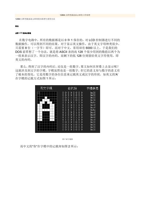
12864点阵型液晶显示屏的工作原理12864点阵型液晶显示屏的基本原理与使用方法转自点阵LCD的显示原理在数字电路中,所有的数据都是以0和1保存的,对LCD控制器进行不同的数据操作,可以得到不同的结果。
对于显示英文操作,由于英文字母种类很少,只需要8位(一字节)即可。
而对于中文,常用却有6000以上,于是我们的DOS前辈想了一个办法,就是将ASCII表的高128个很少用到的数值以两个为一组来表示汉字,即汉字的内码。
而剩下的低128位则留给英文字符使用,即英文的内码。
那么,得到了汉字的内码后,还仅是一组数字,那又如何在屏幕上去显示呢?这就涉及到文字的字模,字模虽然也是一组数字,但它的意义却与数字的意义有了根本的变化,它是用数字的各位信息来记载英文或汉字的形状,如英文的'A'在字模的记载方式如图1所示:图1 “A”字模图而中文的“你”在字模中的记载却如图2所示:图2 “你”字模图12864点阵型LCD简介12864是一种图形点阵液晶显示器,它主要由行驱动器/列驱动器及128×64全点阵液晶显示器组成。
可完成图形显示,也可以显示8×4个(16×16点阵)汉字。
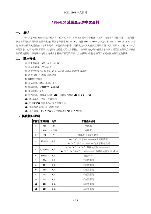
管脚号管脚名称LEVER 管脚功能描述1 VSS 0 电源地2 VDD +5.0V 电源电压3 V0 - 液晶显示器驱动电压4 D/I(RS) H/L D/I=“H”,表示DB7∽DB0为显示数据D/I=“L”,表示DB7∽DB0为显示指令数据5 R/W H/L R/W=“H”,E=“H”数据被读到DB7∽DB0R/W=“L”,E=“H→L”数据被写到IR或DR 6 E H/L R/W=“L”,E信号下降沿锁存DB7∽DB0R/W=“H”,E=“H”DDRA M数据读到DB7∽DB07 DB0 H/L 数据线8 DB1 H/L 数据线9 DB2 H/L 数据线10 DB3 H/L 数据线11 DB4 H/L 数据线12 DB5 H/L 数据线13 DB6 H/L 数据线14 DB7 H/L 数据线15 CS1 H/L H:选择芯片(右半屏)信号16 CS2 H/L H:选择芯片(左半屏)信号17 RET H/L 复位信号,低电平复位18 VOUT -10V LCD驱动负电压19 LED+ - LED背光板电源20 LED- - LED背光板电源表1:12864LCD的引脚说明在使用12864LCD前先必须了解以下功能器件才能进行编程。
LCD12864中文资料
12864LCD液晶显示屏中文资料一、概述带中文字库的128X64是一种具有4位/8位并行、2线或3线串行多种接口方式,内部含有国标一级、二级简体中文字库的点阵图形液晶显示模块;其显示分辨率为128×64, 内置8192个16*16点汉字,和128个16*8点ASCII字符集.利用该模块灵活的接口方式和简单、方便的操作指令,可构成全中文人机交互图形界面。
可以显示8×4行16×16点阵的汉字. 也可完成图形显示.低电压低功耗是其又一显著特点。
由该模块构成的液晶显示方案与同类型的图形点阵液晶显示模块相比,不论硬件电路结构或显示程序都要简洁得多,且该模块的价格也略低于相同点阵的图形液晶模块。
二、基本特性(1)低电源电压(VDD:+3.0--+5.5V)(2)显示分辨率:128×64点(3)内置汉字字库,提供8192个16×16点阵汉字(简繁体可选)(4)内置 128个16×8点阵字符(5)2MHZ时钟频率(6)显示方式:STN、半透、正显(7)驱动方式:1/32DUTY,1/5BIAS(8)视角方向:6点(9)背光方式:侧部高亮白色LED,功耗仅为普通LED的1/5—1/10(10)通讯方式:串行、并口可选(11)内置DC-DC转换电路,无需外加负压(12)无需片选信号,简化软件设计(13)工作温度: 0℃ - +55℃ ,存储温度: -20℃ - +60℃三、模块接口说明*注释1:如在实际应用中仅使用串口通讯模式,可将PSB接固定低电平,也可以将模块上的J8和“GND”用焊锡短接。
*注释2:模块内部接有上电复位电路,因此在不需要经常复位的场合可将该端悬空。
*注释3:如背光和模块共用一个电源,可以将模块上的JA、JK用焊锡短接。
控制器接口信号说明:1、RS,R/W的配合选择决定控制界面的4种模式:2、E信号● 忙标志:BF BF标志提供内部工作情况.BF=1表示模块在进行内部操作,此时模块不接受外部指令和数据.BF=0时,模块为准备状态,随时可接受外部指令和数据.利用STATUS RD 指令,可以将BF读到DB7总线,从而检验模块之工作状态.● 字型产生ROM(CGROM)字型产生ROM(CGROM)提供8192个此触发器是用于模块屏幕显示开和关的控制。
配套液晶PDF资料 12864G中文说明书

序号 1 2 3 4 5 6 7
内容标题 概述 特点 外形及接口引脚功能 基本原理 技术参数 时序特性 指令功能及硬件接口与编程案例
页码 2 2
3~4 4~5 5~6 6~9 9~23
1
1.概述
12864G 型液晶模块由于使 用方便、显示清晰,广泛应用于各种人机交流面板。 2864G 可以显示 128 列*64 行点阵单色图片,或显示 8 个/行*4 行 16*16 点阵的汉字, 或显示 16 个/行*8 行 8*8 点阵的英文、数字、符号。
9
指令名称
RS
(1)显示开/关
0
(display on/off)
指令表
表 8.
指令码
DB7 DB6 DB5 DB4 DB3 DB2 DB1 DB0
1 0 1 0 1 1 1 0 显示开/关:
1 0:关,1:开
说明
(2)显示初始行设置 0 (Display start line set)
(3)页地址设置
5.技术参数
5.1 最大极限参数(超过极限参数则会损坏液晶模块)
名称
符号
标准值
单位
最小
典型
最大
电路电源
VDD - VSS -0.3
7.0
V
LCD 驱动电压 VDD – V0 VDD - 13.5
VDD + 0.3
V
ห้องสมุดไป่ตู้
静电电压
-
-
100
V
工作温度
-10
+60
℃
储存温度
-20
+70
℃
表 2:最大极限参数
5
12864系列点阵型液晶显示模块+
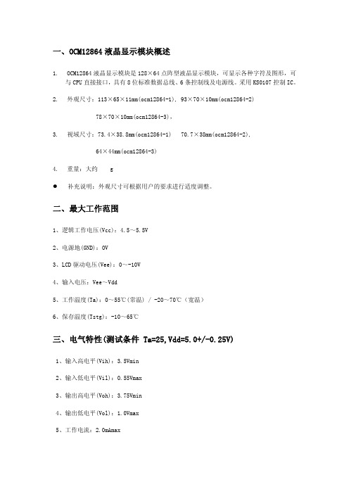
一、OCM12864液晶显示模块概述1.OCM12864液晶显示模块是128×64点阵型液晶显示模块,可显示各种字符及图形,可与CPU直接接口,具有8位标准数据总线、6条控制线及电源线。
采用KS0107控制IC。
2.外观尺寸:113×65×11mm(ocm12864-1), 93×70×10mm(ocm12864-2)78×70×10mm(ocm12864-3),3.视域尺寸:73.4×38.8mm(ocm12864-1) 70.7×38mm(ocm12864-2),64×44mm(ocm12864-3)4.重量:大约 gz补充说明:外观尺寸可根据用户的要求进行适度调整。
二、最大工作范围1、逻辑工作电压(Vcc):4.5~5.5V2、电源地(GND):0V3、LCD驱动电压(Vee):0~-10V4、输入电压:Vee~Vdd5、工作温度(Ta):0~55℃(常温) / -20~70℃(宽温)6、保存温度(Tstg):-10~65℃三、电气特性(测试条件 Ta=25,Vdd=5.0+/-0.25V)1、输入高电平(Vih):3.5Vmin2、输入低电平(Vil):0.55Vmax3、输出高电平(Voh):3.75Vmin4、输出低电平(Vol):1.0Vmax5、工作电流:2.0mAmax四、接口说明1.12864-1,12864-2接口说明表管脚号 管脚 电平 说明1 VSS 0V 逻辑电源地。
2 VDD 5.0V 逻辑电源正。
3 V0 LCD驱动电压,应用时在VEE与V0之间加一2K可调电阻。
4 D/I H/L 数据\指令选择:高电平:数据D0-D7将送入显示RAM;低电平:数据D0-D7将送入指令寄存器执行。
5 R/W H/L 读\写选择: 高电平:读数据;低电平:写数据。
6 E H.H/L 读写使能,高电平有效,下降沿锁定数据。
12864液晶显示模块概述
TC
13,000
Address setup time
TAS
1,500
Address hold time
TAH
1,500
Data setup time
TDDR
1,000
Unit KHz UNIT
ns ns ns ns ns ns ns
ns ns ns ns
使用说明书
Data hold time Enable pulsewidth Enable rise/fall time
2、 “RE”为基本指令集与扩充指令集的选择控制位元,当变更“RE”位元后,往后的指令集将维 持在最后的状态,除非再次变更“RE”位元,否则使用相同指令集时,不需每次重设“RE”位元。
72us
读出 RAM
从 内 部 RAM 读 取 资 料
的值
1 1 D7 D6 D5 D4 D3 D2 D1 D0 (DDRAM/CGRAM/IRAM/GDRAM)
72us
指令表—2:(RE=1:扩充指令集)
指令
指令码
RS RW DB7 DB6 DB5 DB4 DB3 DB2 DB1 DB0
说明
执行时间 (540KHZ)
8 RS
H/L H: Data L: Instruction Code
9 NC
- 空脚
10 /RST
H/L Reset Signal 低电平有效
注K
背光源负极(LED-OV)
引脚 名称 11 DB0 12 DB1 13 DB2 14 DB3 15 DB4 16 DB5 17 DB6 18 DB7 19 NC 20 NC
A
方向 说明 I/O 数据 0 I/O 数据 1 I/O 数据 2 I/O 数据 3 I/O 数据 4 I/O 数据 5 I/O 数据 6 I/O 数据 7
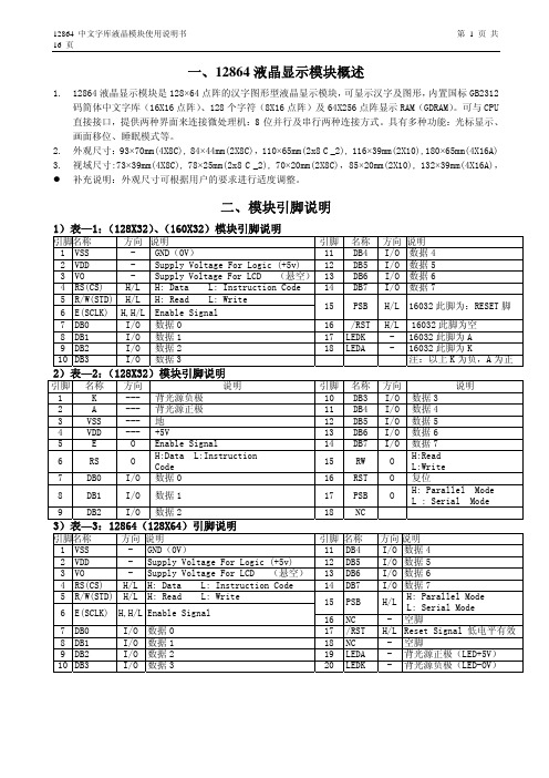
12864中文图形点阵液晶显示模块使用说明书
72us
读出 RAM
的值
1 1 D7
D6
D5
D4
D3
D2
D1
D0
从 内 部 RAM 读 取 数 据 (DDRAM/CGRAM/GDRAM)
72us
指令表 2:(RE=1:扩充指令集)
指令
指令码
RS RW DB7 DB6 DB5 DB4 DB3 DB2 DB1 DB0
说明
执行 时间 (540K HZ)
功能:设定 CGRAM 地址到地址计数器(AC),需确定扩充指令中 SR=0(卷动地址或 RAM 地址选择)
地址
设定 CGRAM 地址到地址计数器(AC)
1 AC5 AC4 AC3 AC2 AC1 AC0 需确定扩充指令中 SR=0(卷动地址或 72us RAM 地址选择)
设定 DDRAM 0 0 1 AC6 AC5 AC4 AC3 AC2 AC1 AC0 设定 DDRAM 地址到地址计数器(AC) 72us
I/O
DB5
I/O
DB6
I/O
DB7
I/O
PSB
I
NC
-
/RST
I
VEE
-
LED+
-
LED-
-
说明
电源地
逻辑电源正(+5V)
LCD 对比度调节电压
并行模式时选择数据或指令
H: 数据 L: 指令
串行模式时选择模块与否
H: 选择 L: 不选择
并行模式时控制读写
H: 读
L: 写
串行模式时输入数据
并行模式时使能端
L
L
L
H
DL
X
RE
X
12864液晶说明手册
一、液晶显示模块概述FM12864M汉字图形点阵液晶显示模块,可显示汉字及图形,内置8192个中文汉字(16X16点阵)、128个字符(8X16点阵)及64X256点阵显示RAM(GDRAM)。
主要技术参数和显示特性:电源:VDD 3.3V~+5V(内置升压电路,无需负压);显示内容:128列× 64行显示颜色:黄绿显示角度:6:00钟直视LCD类型:STN与MCU接口:8位或4位并行/3位串行配置LED背光多种软件功能:光标显示、画面移位、自定义字符、睡眠模式等二、外形尺寸外观尺寸:93×70×12.5mm 视域尺寸:73×39mm二、模块引脚说明17128X64HZ 引脚说明引脚号引脚名称方向功能说明1 VSS - 模块的电源地2 VDD +5V 模块的电源正端3 V0 - LCD驱动电压输入端4 RS(CS) H/L 并行的指令/数据选择信号;串行的片选信号5 R/W(SID) H/L 并行的读写选择信号;串行的数据口6 E(CLK) H/L 并行的使能信号;串行的同步时钟7 DB0 H/L 数据08 DB1 H/L 数据19 DB2 H/L 数据210 DB3 H/L 数据311 DB4 H/L 数据412 DB5 H/L 数据513 DB6 H/L 数据614 DB7 H/L 数据715 PSB H/L 并/串行接口选择:H-并行;L-串行16 NC 空脚17 RESET H/L 复位低电平有效18 NC 空脚19 LED_A (LED+5V)背光源正极20 LED_K (LED-OV)背光源负极逻辑工作电压(VDD):4.5~5.5V电源地(GND):0V工作温度(Ta):-10℃~60℃(常温) / -20℃~70℃(宽温)三、接口时序模块有并行和串行两种连接方法(时序如下):8位并行连接时序图MPU写资料到模块串行数据传送共分三个字节完成:第一字节:串口控制—格式11111ABCA为数据传送方向控制:H表示数据从LCD到MCU,L表示数据从MCU 到LCDB为数据类型选择:H表示数据是显示数据,L表示数据是控制指令C固定为0第二字节:(并行)8位数据的高4位—格式DDDD0000第三字节:(并行)8位数据的低4位—格式0000DDDD串行接口时序参数:(测试条件:T=25℃VDD=4.5V)四、用户指令集1、指令表1:(RE=0:基本指令集)指令指令码说明执行时间(540KHZ)RS RW DB7 DB6 DB5 DB4 DB3 DB2 DB1 DB0清除显示 0 0 0 0 0 0 0 0 0 1 将DDRAM填满“20H”,并且设定DDRAM 的地址计数器(AC)到“00H” 4.6ms地址归位 0 0 0 0 0 0 0 0 1 X 设定DDRAM的地址计数器(AC)到“00H”,并且将游标移到开头原点位置;这个指令并不改变DDRAM的内容 4.6ms进入点设定 0 0 0 0 0 0 0 1 I/D S 指定在资料的读取与写入时,设定游标移动方向及指定显示的移位 72us显示状态开/关 0 0 0 0 0 0 1 D C B D=1:整体显示ONC=1:游标ONB=1:游标位置ON 72us游标或显示移位控制 0 0 0 0 0 1 S/C R/L X X 设定游标的移动与显示的移位控制位元;这个指令并不改变DDRAM的内容 72us功能设定 0 0 0 0 1 DL X 0RE X X DL=1 (必须设为1)RE=1:扩充指令集动作RE=0:基本指令集动作 72us设定CGRAM地址 0 0 0 1 AC5 AC4 AC3 AC2 AC1 AC0 设定CGRAM 地址到地址计数器(AC) 72us设定DDRAM地址 0 0 1 AC6 AC5 AC4 AC3 AC2 AC1 AC0 设定DDRAM地址到地址计数器(AC) 72us读取忙碌标志(BF)和地址 0 1 BF AC6 AC5 AC4 AC3 AC2 AC1 AC0 读取忙碌标志(BF)可以确认内部动作是否完成,同时可以读出地址计数器(AC)的值 0us写资料到RAM 1 0 D7 D6 D5 D4 D3 D2 D1 D0 写入资料到内部的RAM (DDRAM/CGRAM/IRAM/GDRAM) 72us读出RAM的值 1 1 D7 D6 D5 D4 D3 D2 D1 D0 从内部RAM读取资料(DDRAM/CGRAM/IRAM/GDRAM) 72us指令表—2:(RE=1:扩充指令集)指令指令码说明执行时间(540KHZ)RS RW DB7 DB6 DB5 DB4 DB3 DB2 DB1 DB0待命模式 0 0 0 0 0 0 0 0 0 1 将DDRAM填满“20H”,并且设定DDRAM 的地址计数器(AC)到“00H” 72us卷动地址或IRAM地址选择 0 0 0 0 0 0 0 0 1 SR SR=1:允许输入垂直卷动地址SR=0:允许输入IRAM地址 72us反白选择 0 0 0 0 0 0 0 1 R1 R0 选择4行中的任一行作反白显示,并可决定反白与否 72us睡眠模式 0 0 0 0 0 0 1 SL X X SL=1:脱离睡眠模式SL=0:进入睡眠模式 72us扩充功能设定 0 0 0 0 1 1 X 1RE G 0 RE=1:扩充指令集动作RE=0:基本指令集动作G=1 :绘图显示ONG=0 :绘图显示OFF 72us设定IRAM地址或卷动地址 0 0 0 1 AC5 AC4 AC3 AC2 AC1 AC0 SR=1:AC5—AC0为垂直卷动地址SR=0:AC3—AC0为ICON IRAM地址 72us设定绘图RAM地址 0 0 1 AC6 AC5 AC4 AC3 AC2 AC1 AC0 设定CGRAM地址到地址计数器(AC) 72us备注:1、当模块在接受指令前,微处理顺必须先确认模块内部处于非忙碌状态,即读取BF标志时BF需为0,方可接受新的指令;如果在送出一个指令前并不检查BF标志,那么在前一个指令和这个指令中间必须延迟一段较长的时间,即是等待前一个指令确实执行完成,指令执行的时间请参考指令表中的个别指令说明。
12864数据手册
SPECIFICATIONRevision: 1.4CMF-GG1P0104DTSW-W-ETRULY SEMICONDUCTORS LTD: CUSTOMER:PRODUCT : LCD MODULE MODEL NO.: CMF-GG1P0104DTSW-W-ESUPPLIER :TRULY SEMICONDUCTORS LTD. DATE :December 13, 2006REVISION RECORDREV NO.REV DATECONTENTS REMARKS 0.1 2006-04-28 First Release Preliminary1.0 2006-05-08 Full specification 1.1 2006-05-26Amend the drawingP .5 1.2 2006-07-05Amend backlight characteristics andapplication circuit P .7,P .8,P .121.3 2006-07-13 Add FPC layout P .6 1.4 2006-12-13Update the part NO.CONTENTSGENERAL INFORMATIONEXTERNAL DIMENSIONSABSOLUTE MAXIMUM RATINGSELECTRICAL CHARACTERISTICSTIMING OF POWER SUPPLYBACKLIGHT CHARACTERISTICSELECTRO-OPTICAL CHARACTERISTICSINTERFACE DESCRIPTIONREFERENCE APPLICATION CIRCUITREFERENCE INITIAL CODERELIABILITY TESTINSPECTION CRITERIONPRECAUTIONS FOR USING LCD MODULESPACKING SPECIFICATIONPRIOR CONSULT MATTERFACTORY CONTACT INFORMATIONWRITTEN BY CHECKED BY APPROVED BY ZHOU ZHAO YU LIU JIA LIN MING CHUANGENERAL INFORMATIONUnit Item Contents LCD Type FSTN TRANSMISSIVE /Viewing direction 6:00 O’ ClockGlass area (W × H) 34.50 × 35.50 mm2× 24.60 mm2Viewing area (W×H) 30.60× 20.76 mm2Active area (W×H) 26.85Number of Dots 128 × 64 /Dot size (W × H) 0.18 × 0.24 mm2Dot pitch (W × H) 0.21 × 0.27 mm2Pixel size (W × H) 0.18 × 0.24 mm2Pixel pitch (W × H) 0.21 × 0.27 mm2Driver IC ST7565P-G/Backlight Type LED /Module Power consumption / mwInterface Type System parallel interface /Input voltage 2.8 VEXTERNAL DIMENSIONSFPC LAYOUTABSOLUTE MAXIMUM RATINGSUnitMaxParameter Symbol MinV Supply voltage for logic V DD 0.3 5.0V DD + 0.3 VInput voltage V IN -0.3Operating temperature T OP -20 70°C Storage temperature T ST -30 80°CELECTRICAL CHARACTERISTICSDC CHARACTERISTICSTypUnitMaxMinParameter SymbolV2.92.8Supply voltage for logic V DD-V SS 2.7Input Current Idd - 0.27 0.39 mA10.2V10.0Operating voltage for LCD V OP 9.8Input voltage ' H ' level V IH 0.8V DD V DD V DD V0.2V DD VInput voltage ' L ' level V IL 0Output voltage ' H ' level V OH 0.8V DD V DD V DD V0.2V DD VOutput voltage ' L ' level V OL 0TIMING OF POWER SUPPLYPLEASE REFER TO THE DRIVER IC SPECIFICATION.BACKLIGHT CHARACTERISTICSELECTRO-OPTICAL CHARACTERISTICSItem Symbol Condition Min Typ Max Unit Remark NoteTr --- 120 --- ms FIG.3 2 Response timeTf --- 155 --- ms FIG.3 2 Surface Luminance Lv θ=0° ∅=0°Ta=25℃--- --- --- cd/m 2 FIG 4. 1 ∅ = 90°30 40 --- deg ∅ = 270°40 50 --- deg ∅ = 0°30 40 --- deg Viewing angle range θ∅ = 180° 30 40 --- deg FIG 5 3Note 1. Surface luminance is the center point across the LCD surface 500mm from the surface with allpixels displaying white. For more information see FIG 4.Lv = Average Surface Luminance with all white pixels (P 1, P 2, P 3,P 4, P 5)Note 2. Response time is the time required for the display to transition from White to black(Rise Time, Tr) and from black to white(Decay Time, Tf). For additional information see FIG 3.Note 3. Viewing angle is the angle at which the contrast ratio is greater than 2. The angles are determined for the horizontal or x axis and the vertical or y axis with respect to the z axis which is normal to the LCD surface. For more information see FIG 5.FIG. 1 Optical Characteristic Measurement Equipment and Method<Transmissive Mode><Transmissive Mode>FIG. 2FIG. 3The values specified are at an approximate distance 500 m m from the LCD surface at a viewing angle of Φ and θ equal to 0°.Measurement condition : Refer to next pages ( B - light source , Halogen Lamp, with polarizer )FIG. 5 The definition of viewing angle<dimension of viewing angle range>FIG. 4 Measuring method for Contrast ratio,surface luminance , Luminanceuniformity ,CIE (x, y) chromaticity<measuring point for luminance variation><measuring point for surface luminance>VA : 5 mmB : 5 mm Light source spot size ∅=2mm H,V : Active Areameasurement device is TOPCON luminance meter BM-7INTERFACE DESCRIPTIONPin No. Symbol Level DescriptionGround.1 VSS VSSLED,anode.2 LED+ -LED,cathode.3 LED- -supply.4 VDD 2.8VPowerbus.5~12 D0~D7 H/L DataChipselect.13 /CS H/L14 /RESET H/L System reset pin.15 RS H/L Command/data select input pin.execute control pin.Write16 /WR H/L17 /RD H/L Read execute control pin.Ground.18 VSS VSSGround.19 VSS VSSAPPLICATION CIRCUITINITIAL CODEPlease consult our technical department for detail information.RELIABILITY TESTNo. Test Item Test Condition Inspection after test1 HighTemperatureStorage 80±2℃/200 hours2 LowTemperatureStorage -30±2℃/200 hours3 High TemperatureOperating70±2℃/120 hours4 Low TemperatureOperating-20±2℃/120 hours5 TemperatureCycle -20±2℃~25~70±2℃×10cycles(30min.) (5min.) (30min.)6 DampProofTest 50℃±5℃×90%RH/120 hours7 VibrationTest Frequency:10Hz~55Hz~10Hz Amplitude:1.5mm,X,Y,Z direction for total 3hours (Packing condition)8Drooping test Drop to the ground from 1m height, one time, every side of carton.(Packing condition)9ESD test Voltage:±8KV R: 330ΩC:150pFAir discharge, 10timeInspection after2~4hours storageat roomtemperature, thesample shall befree from defects:1.Air bubble in theLCD;2.Sealleak;3.Non-display;4.missing segments;5.Glass crack;6.Current Idd is twicehigher than initialvalue.Remark:1.The test samples should be applied to only one test item.2.Sample size for each test item is 5~10pcs.3.For Damp Proof Test, Pure water(Resistance>10MΩ) should be used.4.In case of malfunction defect caused by ESD damage, if it would be recovered to normalstate after resetting, it would be judge as a good part.5.EL evaluation should be excepted from reliability test with humidity and temperature:Some defects such as black spot/blemish can happen by natural chemical reaction with humidity and Fluorescence EL has.6.Failure Judgment Criterion: Basic Specification, Electrical Characteristic, MechanicalCharacteristic, Optical Characteristic.7.Please use automatic switch menu(or roll menu) testing mode when test operating mode.TITLE:FUNCTIONAL TEST & INSPECTION CRITERIA MDS Product4.3. Cosmetic Defect Item NoItems to be inspectedInspection StandardClassification ofdefects(i) Chips on cornerNotes: S=contact pad lengthChips on the corner of terminal shall not be allowed to extend into the ITO pad or expose perimeter seal. X Y Z ≤2.0≤SDisregardMinor(ii)Usual surface cracksX Y Z ≤3.0<Inner border line of the sealDisregardMinor4.3.5Glass defect(iii) CrackCracks tend to break are not allowed.Major4.3.6Parts alignment1) Not allow IC and FPC/heat-seal lead width is more than50% beyond lead pattern. 2) Not allow chip or solder component is off center more than50% of the pad outline.MinorPRECAUTIONS FOR USING LCD MODULESHanding Precautions (1) The display panel is made of glass and polarizer. As glass is fragile. It tends to become or chipped during handling especially on the edges. Please avoid dropping or jarring. Do not subject it to a mechanical shock by dropping it or impact.(2) If the display panel is damaged and the liquid crystal substance leaks out, be sure not to get any in your mouth. If the substance contacts your skin or clothes, wash it off using soap and water.(3) Do not apply excessive force to the display surface or the adjoining areas since this may cause the color tone to vary. Do not touch the display with bare hands. This will stain the display area and degraded insulation between terminals (some cosmetics are determined to the polarizer).(4) The polarizer covering the display surface of the LCD module is soft and easily scratched. Handle this polarizer carefully. Do not touch, push or rub the exposed polarizers with anything harder than an HB pencil lead (glass, tweezers, etc.). Do not put or attach anything on the display area to avoid leaving marks on. Condensation on the surface and contact with terminals due to cold will damage, stain or dirty the polarizer. After products are tested at low temperature they must be warmed up in a container before coming is contacting with room temperature air.(5) If the display surface becomes contaminated, breathe on the surface and gently wipe it with a soft dry cloth. If it is heavily contaminated, moisten cloth with one of the following solvents - Isopropyl alcohol - Ethyl alcoholDo not scrub hard to avoid damaging the display surface.(6) Solvents other than those above-mentioned may damage the polarizer. Especially, do not use the following. - Water - Ketone - Aromatic solventsWipe off saliva or water drops immediately, contact with water over a long period of time may cause deformation or color fading. Avoid contacting oil and fats.(7) Exercise care to minimize corrosion of the electrode. Corrosion of the electrodes is accelerated by water droplets, moisture condensation or a current flow in a high-humidity environment.(8) Install the LCD Module by using the mounting holes. When mounting the LCD module make sure it is free of twisting, warping and distortion. In particular, do not forcibly pull or bend the I /O cable or the backlight cable. (9) Do not attempt to disassemble or process the LCD module. (10) NC terminal should be open. Do not connect anything. (11) If the logic circuit power is off, do not apply the input signals.(12) Electro-Static Discharge Control ,Since this module uses a CMOS LSI, the same careful attention should be paid to electrostatic discharge as for an ordinary CMOS IC. To prevent destruction of the elements by static electricity, be careful to maintain an optimum work environment.- Before remove LCM from its packing case or incorporating it into a set, be sure the module and your body have the same electric potential .Be sure to ground the body when handling the LCD modules. - Tools required for assembling, such as soldering irons, must be properly grounded. make certain the AC power source for the soldering iron does not leak. When using an electric screwdriver to attach LCM, the screwdriver should be of ground potentiality to minimize as much as possible any transmission of electromagnetic waves produced sparks coming from the commutator of the motor.- To reduce the amount of static electricity generated, do not conduct assembling and other work under dry conditions. To reduce the generation of static electricity be careful that the air in the work is not too dried. A relative humidity of 50%-60% is recommended .As far as possible make the electric potential of your work clothes and that of the work bench the ground potential(13)Since LCM has been assembled and adjusted with a high degree of precision, avoid applying excessive shocks to the module or making any alterations or modifications to it.- Do not alter, modify or change the shape of the tab on the metal frame.- Do not make extra holes on the printed circuit board, modify its shape or change the positions of components to be attached.- Do not damage or modify the pattern writing on the printed circuit board.- Absolutely do not modify the zebra rubber strip (conductive rubber) or heat seal connector.- Except for soldering the interface, do not make any alterations or modifications with a soldering iron.- Do not drop, bend or twist LCM.Storage PrecautionsWhen storing the LCD modules, the following precaution is necessary.(1) Store them in a sealed polyethylene bag. If properly sealed, there is no need for the dessicant.(2) Store them in a dark place. Do not expose to sunlight or fluorescent light, keep the temperature between 0°C and 35°C.(3) The polarizer surface should not come in contact with any other objects. (We advise you to store them in the container in which they were shipped).OthersLiquid crystals solidify under low temperature (below the storage temperature range) leading to defective orientation or the generation of air bubbles (black or white). Air bubbles may also be generated if the module is subject to a low temperature.If the LCD modules have been operating for a long time showing the same display patterns, the display patterns may remain on the screen as ghost images and a slight contrast irregularity may also appear. A normal operating status can be regained by suspending use for some time. It should be noted that this phenomenon does not adversely affect performance reliability.To minimize the performance degradation of the LCD modules resulting from destruction caused by static electricity etc., exercise care to avoid holding the following sections when handling the modules.- Exposed area of the printed circuit board.-Terminal electrode sections.USING LCD MODULESInstalling LCD ModulesThe hole in the printed circuit board is used to fix LCM as shown in the picture below. Attend to the following items when installing the LCM.(1) Cover the surface with a transparent protective plate to protect the polarizer and LC cell.(2) When assembling the LCM into other equipment, the spacer to the bit between the LCM and the fitting plate should have enough height to avoid causing stress to the module surface, refer to the individual specifications for measurements. The measurement tolerance should be ±0.1mm.Precaution for assemble the module with BTB connector:Please note the position of the male and female connector position,don’t assemble or assemble likethe method which the following picture showsPrecaution for soldering to the LCMHand soldering Machine drag soldering Machine press solderingNo ROHS product 290°C ~350°C.Time : 3-5S.330°C ~350°C.Speed : 4-8 mm/s.300°C ~330°C.Time : 3-6S.Press: 0.8~1.2MpaROHS product 340°C ~370°C.Time : 3-5S.350°C ~370°C.Time : 4-8 mm/s.330°C ~360°C.Time : 3-6S.Press: 0.8~1.2Mpa(1) If soldering flux is used, be sure to remove any remaining flux after finishing to soldering operation. (This does not apply in the case of a non-halogen type of flux.) It is recommended that you protect the LCD surface with a cover during soldering to prevent any damage due to flux spatters.(2) When soldering the electroluminescent panel and PC board, the panel and board should not be detached more than three times. This maximum number is determined by the temperature and time conditions mentioned above, though there may be some variance depending on the temperature of the soldering iron.Precautions for Operation(1) Viewing angle varies with the change of liquid crystal driving voltage (VLCD). Adjust VLCD to show the best contrast.(2) It is an indispensable condition to drive LCD's within the specified voltage limit since the higher voltage then the limit cause the shorter LCD life.An electrochemical reaction due to direct current causes LCD's undesirable deterioration, so that the use of direct current drive should be avoided.(3) Response time will be extremely delayed at lower temperature than the operating temperature range and on the other hand at higher temperature LCD's show dark color in them.However those phenomena do not mean malfunction or out of order with LCD's, Which will come back in the specified operating temperature.(4) If the display area is pushed hard during operation, the display will become abnormal. However, it will return to normal if it is turned off and then back on.(5) A slight dew depositing on terminals is a cause for electro-chemical reaction resulting in terminal open circuit. Usage under the maximum operating temperature,50%RH or less is required.(6) Input each signal after the positive/negative voltage becomes stable.(7)Please keep the temperature within specified range for use and storage. Polarization degradation, bubble generation or polarizer peel-off may occur with high temperature and high humidity.Safety(1) It is recommended to crush damaged or unnecessary LCDs into pieces and wash them off with solvents such as acetone and ethanol, which should later be burned.(2) If any liquid leaks out of a damaged glass cell and comes in contact with the hands, wash off thoroughly with soap and water.Limited WarrantyUnless agreed between TRULY and customer, TRULY will replace or repair any of its LCD modules which are found to be functionally defective when inspected in accordance with TRULY LCD acceptance standards (copies available upon request) for a period of one year from date of shipments. Cosmetic/visual defects must be returned to TRULY within 90 days of shipment. Confirmation of such date shall be based on freight documents. The warranty liability of TRULY limited to repair and/or replacement on the terms set forth above. TRULY will not be responsible for any subsequent or consequential events.Return LCM under warrantyNo warranty can be granted if the precautions stated above have been disregarded. The typical examples of violations are :- Broken LCD glass.- PCB eyelet is damaged or modified.- PCB conductors damaged.- Circuit modified in any way, including addition of components.- PCB tampered with by grinding, engraving or painting varnish.- Soldering to or modifying the bezel in any manner.Module repairs will be invoiced to the customer upon mutual agreement. Modules must be returned with sufficient description of the failures or defects. Any connectors or cable installed by the customer must be removed completely without damaging the PCB eyelet, conductors and terminals.PACKING SPECIFICATIONTBDPRIOR CONSULT MATTER1.①For Truly standard products, we keep the right to change material, process ... for improving theproduct property without notice on our customer.②For OEM products, if any change needed which may affect the product property, we will consult with our customer in advance.2. If you have special requirement about reliability condition, please let us know before you start the test on our samples.FACTORYFACTORY NAME: TRULY SEMICONDUCTORS LTD.FACTORY ADDRESS: Truly Industrial Area, ShanWei City,GuangDong,ChinaFACTORY PHONE:86-0660-******* FAX: 86-0660-*******。
学习笔记:12864液晶模块的详细使用
学习笔记:12864液晶模块的详细使用备注:这篇文章是对12864操作的具体介绍,仅限刚接触12864的新手,大神请拍砖,文章写的较散,建议先参考12864手册及控制驱动器ST7920英文手册有个初步理解之后再阅读该篇文章,将会有更深的认识。
强烈建议阅读ST7920英文手册,细节内容里面有详细介绍,中文的12864也是从中译过来的。
本文分三个步骤介绍12864的内部资源原理,指令集详细讲解,以及应用例子。
对12864的所有操作概括起来有4种:1)、读忙状态(同时读出指针地址内容),初始化之后每次对12864的读写均要进行忙检测。
2)、写命令:所有的命令可以查看指令表,后续讲解指令的详细用法。
写地址也是写指令。
3)、写数据:操作对象有DDRAM、CGRAM、GDRAM。
4)、读数据:操作对象也是DDRAM、CGRAM、GDRAM。
对12864的学习首相要了解其内部资源,知道了它里面有哪些东西,你就可以更加方便的使用它。
先介绍几个英文的名字:DDRAM:(Data Display Ram),数据显示RAM,往里面写啥,屏幕就会显示啥。
CGROM:(Character Generation ROM),字符发生ROM。
里面存储了中文汉字的字模,也称作中文字库,编码方式有GB2312(中文简体)和BIG5(中文繁体)。
笔者使用的是育松电子的QC12864B,讲解以此为例。
CGRAM:(Character Generation RAM),字符发生RAM,,12864内部提供了64×2B的CGRAM,可用于用户自定义4个16×16字符,每个字符占用32个字节。
GDRAM:(Graphic Display RAM):图形显示RAM,这一块区域用于绘图,往里面写啥,屏幕就会显示啥,它与DDRAM的区别在于,往DDRAM中写的数据是字符的编码,字符的显示先是在CGROM中找到字模,然后映射到屏幕上,而往GDRAM中写的数据时图形的点阵信息,每个点用1bit来保存其显示与否。
12864中文详细资料

12864液晶模块文档带中文字库的128X64是一种具有4位/8位并行、2线或3线串行多种接口方式,内部含有国标一级、二级简体中文字库的点阵图形液晶显示模块;其显示分辨率为128×64, 内置8192个16*16点汉字,和128个16*8点ASCII字符集.利用该模块灵活的接口方式和简单、方便的操作指令,可构成全中文人机交互图形界面。
可以显示8×4行16×16点阵的汉字.也可完成图形显示.低电压低功耗是其又一显著特点。
由该模块构成的液晶显示方案与同类型的图形点阵液晶显示模块相比,不论硬件电路结构或显示程序都要简洁得多,且该模块的价格也略低于相同点阵的图形液晶模块。
基本特性:l 低电源电压(VDD:+3.0--+5.5V)l 显示分辨率:128×64点l 内置汉字字库,提供8192个16×16点阵汉字(简繁体可选)l 内置128个16×8点阵字符l 2MHZ时钟频率l 显示方式:STN、半透、正显l 驱动方式:1/32DUTY,1/5BIASl 视角方向:6点l 背光方式:侧部高亮白色LED,功耗仅为普通LED的1/5—1/10l 通讯方式:串行、并口可选l 内置DC-DC转换电路,无需外加负压l 无需片选信号,简化软件设计l 工作温度: 0℃- +55℃,存储温度: -20℃- +60℃模块接口说明注释1:如在实际应用中仅使用串口通讯模式,可将PSB接固定低电平,也可以将模块上的J8和“GND”用焊锡短接。
*注释2:模块内部接有上电复位电路,因此在不需要经常复位的场合可将该端悬空。
*注释3:如背光和模块共用一个电源,可以将模块上的JA、JK用焊锡短接。
2.2并行接口管脚号管脚名称电平管脚功能描述1 VSS 0V 电源地2 VCC 3.0+5V 电源正3 V0 - 对比度(亮度)调整4RS(CS)H/LRS=“H”,表示DB7——DB0为显示数据RS=“L”,表示DB7——DB0为显示指令数据5R/W(SID) H/L R/W=“H”,E=“H”,数据被读到DB7——DB0R/W=“L”,E=“H→L”, DB7——DB0的数据被写到IR或DR6 E(SCLK) H/L 使能信号7 DB0 H/L 三态数据线8 DB1 H/L 三态数据线9 DB2 H/L 三态数据线10 DB3 H/L 三态数据线11 DB4 H/L 三态数据线12 DB5 H/L 三态数据线13 DB6 H/L 三态数据线14 DB7 H/L 三态数据线15 PSB H/L H:8位或4位并口方式,L:串口方式(见注释1)16 NC - 空脚17 /RESET H/L 复位端,低电平有效(见注释2)18 VOUT - LCD驱动电压输出端19 A VDD 背光源正端(+5V)(见注释3)20 K VSS 背光源负端(见注释3)*注释1:如在实际应用中仅使用并口通讯模式,可将PSB接固定高电平,也可以将模块上的J8和“VCC”用焊锡短接。
12864中文资料
12864中文资料12864中文资料一、OCM12864液晶显示模块概述OCM12864液晶显示模块是128×64点阵型液晶显示模块,可显示各种字符及图形,可与CPU直接接口,具有8位标准数据总线、6条控制线及电源线。
采用KS0107控制IC。
二、最大工作范围1、逻辑工作电压(Vcc):4.5~5.5V2、电源地(GND):0V3、LCD驱动电压(Vee):0~-10V4、输入电压:Vee~Vdd5、工作温度(Ta):0~55℃(常温) / -20~70℃(宽温)6、保存温度(Tstg):-10~65℃三、电气特性(测试条件Ta=25,Vdd=5.0 /-0.25V)1、输入高电平(Vih):3.5Vmin2、输入低电平(Vil):0.55Vmax3、输出高电平(Voh):3.75Vmin4、输出低电平(Vol):1.0Vmax5、工作电流:2.0mAmax四、接口说明12864-1,12864-2接口说明表1 VSS 0V 逻辑电源地。
2 VDD 5.0V 逻辑电源正。
3 V0 LCD驱动电压,应用时在VEE与V0之间加一2K可调电阻。
4 D/I H/L 数据\指令选择:高电平:数据D0-D7将送入显示RAM;低电平:数据D0-D7将送入指令寄存器执行。
5 R/W H/L 读\写选择:高电平:读数据;低电平:写数据。
6 E H.H/L 读写使能,高电平有效,下降沿锁定数据。
7 DB0 H/L 数据输入输出引脚。
8 DB1 H/L 数据输入输出引脚。
9 DB2 H/L 数据输入输出引脚。
10 DB3 H/L 数据输入输出引脚。
11 DB4 H/L 数据输入输出引脚。
12 DB5 H/L 数据输入输出引脚。
13 DB6 H/L 数据输入输出引脚。
14 DB7 H/L 数据输入输出引脚。
15 CS1 H/L 片选择信号,低电平时选择前64列。
16 CS2 H 片选择信号,低电平时选择后64列。
12864详尽中文资料
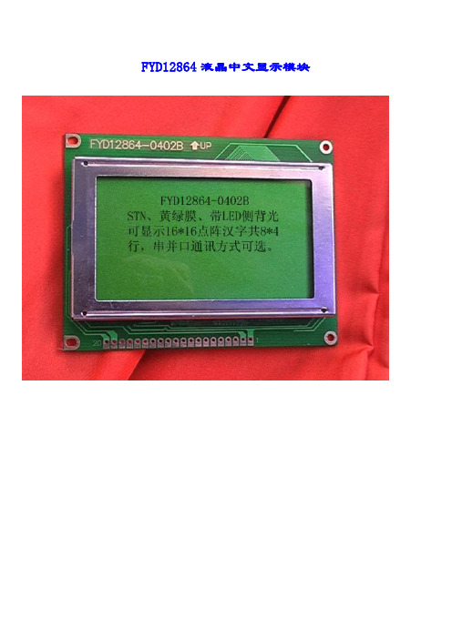
FYD12864液晶中文显示模块(一) (一)概述 (3)(二)(二)外形尺寸1 方框图 (3)2 外型尺寸图 (4)(三)(三)模块的接口 (4)(四)(四)硬件说明 (5)(五) 指令说明 (7)(五)(五)读写操作时序 (8)(六)(六)交流参数 (11)(七)(七)软件初始化过程 (12)(八)(八)应用举例 (13)(九)(九)附录1半宽字符表 (20)2 汉字字符表 (21)一、概述FYD12864-0402B是一种具有4位/8位并行、2线或3线串行多种接口方式,内部含有国标一级、二级简体中文字库的点阵图形液晶显示模块;其显示分辨率为128×64, 内置8192个16*16点汉字,和128个16*8点ASCII字符集.利用该模块灵活的接口方式和简单、方便的操作指令,可构成全中文人机交互图形界面。
可以显示8×4行16×16点阵的汉字. 也可完成图形显示.低电压低功耗是其又一显著特点。
由该模块构成的液晶显示方案与同类型的图形点阵液晶显示模块相比,不论硬件电路结构或显示程序都要简洁得多,且该模块的价格也略低于相同点阵的图形液晶模块。
基本特性:●●低电源电压(VDD:+3.0--+5.5V)●●显示分辨率:128×64点●●内置汉字字库,提供8192个16×16点阵汉字(简繁体可选)●●内置 128个16×8点阵字符●●2MHZ时钟频率●●显示方式:STN、半透、正显●●驱动方式:1/32DUTY,1/5BIAS●●视角方向:6点●●背光方式:侧部高亮白色LED,功耗仅为普通LED的1/5—1/10 ●●通讯方式:串行、并口可选●●内置DC-DC转换电路,无需外加负压●●无需片选信号,简化软件设计●●工作温度: 0℃ - +55℃ ,存储温度: -20℃ - +60℃二、方框图3、外形尺寸图三、模块接口说明*注释1:如在实际应用中仅使用串口通讯模式,可将PSB接固定低电平,也可以将模块上的J8和“GND”用焊锡短接。
12864液晶显示资料及程序
12864液晶显示资料及程序硬件连接方式是:并口直接访问。
这是汉字显示程序:#include<reg51.h>#include<absacc.h>#define uchar unsigned char#define datawr 0x1200 //写数据通道#define comwr 0x1000 //写控制命令通道#define datare 0x1300 //读数据通道#define comre 0x1100 //读忙通道uchar code disp_data[]={" 浙江大学" //第一行,第一页"04级通信工程一班" //第三行" 宁波理工学院" //第二行" 竞赛小组" //第四行"128X64液晶显示器" //第一行,第二页" 测试程序" //第三行" 07年07月25日" //第二行" Tornado "}; //第四行void set12864();void write_command(uchar command);void write_page(uchar data_add);void read_page(uchar data_add);void delays(uchar cont);void main(){while(1){set12864(); //初始化12864write_page(0); //写入一页数据read_page(0x30); //读出一页数据到内部RAMdelays(2); //延时2swrite_page(64); //写入下一页数据delays(2); //延时2s}}//初始化12864子程序void set12864(){write_command(0x30); //功能设定控制字write_command(0x0c); //显示开关控制字write_command(0x01); //清除屏幕控制字write_command(0x06); //进入设定点控制字}//写控制命令子程序void write_command(uchar command){bit flag=1; //12864空闲标志位while(flag) //检查12864是否空闲flag="XBYTE"[comre]&0x80;XBYTE[comwr]=command; //空闲传送控制字}//写一页子程序void write_page(uchar data_add){bit flag=1; //12864空闲标志位uchar num=64; //64个循环,连续写入32个汉字或是64个西文字符write_command(0x80);for(;num>0;num--){while(flag) //检查12864是否空闲flag="XBYTE"[comre]&0x80;XBYTE[datawr]=disp_data[data_add++]; //空闲传送数据}}//读一页子程序void read_page(uchar data_add){bit flag=1; //12864空闲标志位uchar num=64; //64个循环,连续写入32个汉字或是64个西文字符write_command(0x80);for(;num>0;num--){while(flag) //检查12864是否空闲flag="XBYTE"[comre]&0x80;DBYTE[data_add++]=XBYTE[datare]; //空闲传送数据}}//延时cont秒子程序void delays(uchar count){unsigned char h,i,j,k;do{for(h=5;h>0;h--)for(i=4;i>0;i--)for(j=116;j>0;j--)for(k=214;k>0;k--);}while(--count);}这是图象显示程序:#include<reg51.h>#include<absacc.h>#define uchar unsigned char#define uint unsigned int#define datawr 0x1200 //写数据通道#define comwr 0x1000 //写控制命令通道#define datare 0x1300 //读数据通道#define comre 0x1100 //读忙通道uchar code disp_data[] = // 数据表{0x00,0x01,0x3F,0xFF,0xFF,0xFF,0xFF,0xFF,0xFF,0xFF,0xFF,0x00,0x00 ,0x00,0x00,0x00,0x00,0x01,0x7F,0xFF,0xFF,0xFF,0xFF,0xFF,0xFF,0xFF,0xFF,0x80,0x00 ,0x00,0x00,0x00,0x00,0x07,0xFF,0xFF,0xFF,0xFF,0xFF,0xFF,0xFF,0xFF,0xFF,0xC0,0x00 ,0x00,0x00,0x00,0x00,0x07,0xFF,0xFF,0xFF,0xFF,0xFF,0xFF,0xFF,0xFF,0xFF,0xE0,0x00 ,0x00,0x00,0x00,0x00,0x0F,0xFF,0xFF,0xFF,0xFF,0xFF,0xFF,0xFF,0xFF,0xFF,0xF0,0x00 ,0x00,0x00,0x00,0x00,0x0F,0xFF,0xFF,0xFF,0xFF,0xFF,0xFF,0xFF,0xFF,0xFF,0xF8,0x00 ,0x00,0x00,0x00,0x00,0x1F,0xFF,0xFF,0xFF,0xFF,0xFF,0xFF,0xFF,0xFF,0xFF,0xFC,0x0 0,0x00,0x00,0x00,0x00,0x3F,0xFF,0xFF,0xFF,0xFF,0xFF,0xFF,0xFF,0xFF,0xFF,0xFE,0x8 0,0x00,0x00,0x00,0x00,0x7F,0xFF,0xFF,0xFF,0xFF,0xFF,0xFF,0xFF,0xFF,0xFF,0xFF,0xF F,0xFF,0xFF,0xFF,0x00,0xFF,0xFF,0xFF,0xFF,0xFF,0xFF,0xFF,0xFF,0xFF,0xFF,0xFF,0xF0x00,0xFF,0xFF,0xFF,0xFF,0xFF,0xFF,0xFF,0xFF,0xFF,0xFF,0xFF,0x0 3,0xFF,0xFF,0xFF,0x00,0xFF,0xFF,0xFF,0xFF,0xFF,0xFF,0xFF,0xFF,0xFF,0xFF,0xFF,0x0 0,0x07,0xFF,0xFF,0x01,0xFF,0xFF,0xFF,0xFF,0xFF,0xFF,0xFF,0xFF,0xFF,0xFF,0xFF,0x8 0,0x00,0x0B,0xFF,0x01,0xFF,0xFF,0xFF,0xFF,0xFF,0xFF,0xFF,0xFF,0xFF,0xFF,0xFF,0x8 0,0x00,0x00,0x1F,0x01,0xFF,0xFF,0xFF,0xFF,0x7F,0xFF,0xFF,0xFF,0xFF,0xFF,0xFF,0xC 0,0x00,0x00,0x00,0x01,0xFF,0xFF,0xFF,0xF3,0x79,0xFF,0xFF,0xFF,0xFF,0xFF,0xFF,0xC 0,0x00,0x00,0x00,0x03,0xFF,0xFF,0xFF,0xE6,0x62,0xFF,0xFF,0xFF,0xFF,0xFF,0xFF,0xE 1,0x60,0x00,0x68,0x01,0xFF,0xFF,0xFE,0x00,0x60,0xFF,0xFF,0xFF,0xFF,0xFF,0xFF,0xE1 ,0x00,0x00,0x0E,0x01,0xFF,0xFF,0xF8,0x00,0x4B,0xFF,0xFF,0xFF,0xFF,0xFF,0xFF,0xF0 ,0x8E,0x08,0x79,0x07,0xFF,0xFF,0xF0,0x00,0x41,0xFF,0xFF,0xFF,0xFF,0xFF,0xFF,0xE6 ,0xC0,0x07,0x61,0xC3,0xFF,0xFE,0xC0,0x00,0x00,0x7F,0xFF,0xFF,0xFF,0xFF,0xFF,0xF F,0xED,0xEF,0x3F,0x83,0xFF,0xFE,0x60,0x00,0x00,0x7F,0xFF,0xFF,0xFF,0xFF,0xFF,0xFF ,0xFF,0xFF,0xFF,0xC0,0xFF,0xFD,0xFC,0x6C,0x00,0x3F,0xFF,0xFF,0xFF,0xFF,0xFF,0xF F,0xFF,0xFF,0xFF,0xF0,0x7F,0xF3,0xFF,0xFE,0x60,0x3F,0xFF,0xFF,0xFF,0xFF,0xFF,0xFF ,0xFF,0xFF,0xFF,0xFF,0xFF,0xF3,0xFF,0xFF,0x50,0x1F,0xFF,0xFF,0xFF,0xFF,0xFF,0xF F,0xFF,0xFF,0xC9,0xFB,0xFF,0xF1,0xF8,0x8C,0xD8,0x1F,0xFF,0xFF,0xFF,0xFF,0xFF,0xF F,0xFB,0x6F,0xD9,0xC2,0x3F,0xF8,0x40,0x00,0x00,0x1F,0xFF,0xFF,0xFF,0xFF,0xFF,0xF6 ,0xDF,0x1E,0xFF,0xFF,0x7F,0xFC,0x38,0x00,0x00,0x1F,0xFF,0xFF,0xFF,0xFF,0xFF,0x64 ,0x2F,0x6F,0xFF,0xFD,0x7B,0xFC,0x1F,0xE0,0x00,0x1F,0xFF,0xFF,0xFF,0xFF,0xFF,0x5 F,0x7C,0xEE,0xFF,0xC7,0xFF,0xBC,0x0F,0xFF,0x00,0x03,0xFF,0xFF,0xFF,0xFF,0xFF,0xD F,0xFE,0xEF,0xFF,0xFF,0xE7,0xDC,0x07,0xE7,0xF8,0x12,0x7F,0xFF,0xFF,0xFF,0xFF,0x4 7,0xFF,0xFF,0xFF,0xFF,0xE7,0x80,0x03,0xF4,0x00,0x00,0x5F,0xFF,0xFF,0xFE,0xFE,0xE30xFF,0xFE,0xC0,0x01,0xC0,0x00,0x00,0x1B,0xFF,0xFF,0xFB,0xFF,0xF F,0xFF,0xFF,0xFF,0x7F,0xEE,0xC0,0x00,0xC0,0x00,0x00,0x03,0xFF,0xFF,0xFF,0xFF,0xFF ,0xFF,0xFF,0xFF,0xFE,0x98,0x00,0x00,0x00,0x00,0x00,0x03,0xFF,0xFF,0xEF,0xFF,0xFF, 0xFF,0xFF,0xFF,0x20,0x0E,0x60,0x00,0x00,0x00,0x00,0x00,0xFF,0xFF,0x8F,0xFF,0xFF, 0xFF,0xFF,0xFF,0x05,0x80,0xE0,0x00,0x00,0x00,0x00,0x01,0xFF,0xFD,0xFF,0xFF,0xFF, 0xFF,0xFF,0xFF,0x09,0x80,0xA0,0x00,0x00,0x00,0x00,0x01,0xFF,0xFF,0x7F,0xFF,0xFF, 0xFF,0xFF,0xFF,0x85,0x2A,0xC0,0x00,0x00,0x00,0x00,0x01,0xFF,0xFB,0xFF,0xFF,0xFF, 0xFF,0xFF,0xFE,0xBF,0xF3,0xC0,0x00,0x00,0x00,0x00,0x00,0xFF,0xF7,0xFF,0xFF,0xFF, 0xFF,0xFF,0xF8,0xFF,0xFF,0x80,0x00,0x00,0x00,0x00,0x01,0xFF,0xE0,0xFF,0xFF,0xFF, 0xFF,0xFF,0x00,0xFF,0xFF,0x80,0x00,0x00,0x00,0x00,0x00,0xFF,0xC0,0xFF,0xFF,0xFF, 0xFF,0xC0,0x1F,0xFF,0xFF,0x80,0x00,0x40,0x00,0x00,0x00,0xFF,0x80,0xFF,0xFF,0xFF, 0x80,0x07,0xFF,0xFF,0xFF,0xC0,0x00,0xC0,0x00,0x00,0x01,0xFF,0x01,0xFF,0xFF,0xF8 ,0x00,0xFF,0xFF,0xFF,0xFF,0xE0,0x63,0x80,0x00,0x00,0x01,0xFE,0x01,0xFF,0x18,0x00, 0x3F,0xFF,0xFF,0xFF,0xFF,0xFE,0x00,0x00,0x00,0x00,0x01,0xCC,0x01,0xFE,0x00,0x07, 0xFF,0xFF,0xFF,0xFF,0xFF,0xFE,0x00,0x00,0x00,0x00,0x07,0xA0,0x03,0xFC,0x00,0xFF, 0xFF,0xFF,0xFF,0xFF,0xFF,0xFE,0x00,0x00,0x00,0x00,0x05,0xC0,0x03,0xC8,0x00,0x7F, 0xFF,0xFF,0xFF,0xFF,0xFF,0xFE,0x00,0x00,0x00,0x00,0x19,0x00,0x00,0x88,0x0C,0x07, 0xFF,0xFF,0xFF,0xFF,0xFF,0xFC,0x00,0x0C,0x00,0x00,0x00,0x00,0x01,0x00,0x01,0xC0, 0x7F,0xFF,0xFF,0xFF,0xFF,0xF8,0x07,0x0F,0x80,0x00,0x00,0x00,0x00,0x00,0x00,0x38,0 x0F,0xFF,0xFE,0xFF,0xFF,0xD0,0x07,0xFF,0xC0,0x00,0x00,0x00,0x00,0x00,0x00,0x0F, 0x03,0xFF,0xF8,0xFF,0xFC,0x00,0x00,0x60,0x00,0x00,0x00,0x00,0x00,0x00,0x00,0x00,0 x3F,0xFF,0xC0,0xFF,0xF0,0x00,0x00,0x00,0x00,0x00,0x00,0x00,0x20,0x00,0x00,0x00,00xFF,0xE0,0x00,0x00,0x00,0x00,0x00,0x00,0x00,0x80,0x00,0x00,0x00,0 x00,0x1F,0xFE,0xFF,0xC0,0x00,0x00,0x00,0x00,0x00,0x78,0x02,0x00,0x00,0x00,0x00,0 x00,0x0F,0xFF,0xFF,0x00,0x00,0x00,0x00,0x00,0x03,0xF0,0x78,0x00,0x00,0x00,0x00,0 x00,0x02,0xFF,0xFE,0x00,0x00,0x00,0x00,0x00,0x1F,0xFF,0xF0,0x00,0x00,0x00,0x00, 0x00,0x00,0x7F,0xF0,0x00,0x00,0x00,0x00,0x00,0x7F,0xFF,0xC0,0x00,0x00,0x00,0x00, 0x00,0x00,0x1F,0xE0,0x00,0x00,0x00,0x00,0x00,0x3F,0xFF,0x80,0x00,0x00,0x00,0x00,0 x00,0x00,0x1F,0x00,0x00,0x00,0x00,0x00,0x00,0x0F,0xFF,0x00,0x00,0x00,0x00,0x00,0 x00,0x00,0x27,0xC0,0x00,0x00,0x00,0x00,0x00,0x01,0xFC,0x00,0x00,0x00,0x00,0x00, 0x00,0x00,0x01,0x80,0x00,0x00,0x00,0x00,0x00,0x00,0x00,0x00,0x00,0x00,0x00,0x00,0 x00,0x00,0x04,0x80,0x00,0x00,0x00,0x00,0x00,0x08,0x00,0x00,0x00,0x00,0x00,0x00,0 x00,0x00,0x01};void set12864();void setxy(uchar x,uchar y);void write_command(uchar command);void write_16byte(uint data_add);void delays(uchar count);void main(){uchar x,y,i;while(1){y="0x80"; //设置液晶上半部分坐标x="0x80";delays(2); //延时2sset12864(); //初始化12864delays(2);for(i=0;i<32;i++) //写入液晶上半图象部分{ //写入坐标setxy(x,y);write_16byte(i*16); //连续写入16字节数据y++; //y轴地址加1}y="0x80"; //设置液晶下半部分坐标x="0x88";for(i=0;i<32;i++) //写入液晶下半图象部分{setxy(x,y); //写入坐标write_16byte((32+i)*16);//连续写入16字节数据y++; //y轴地址加1}write_command(0x34); //写入扩充指令命令write_command(0x36); //显示图象}}//初始化12864子程序void set12864(){write_command(0x30); //功能设定控制字write_command(0x0c); //显示开关控制字write_command(0x01); //清除屏幕控制字write_command(0x06); //进入设定点控制字}//设置绘图坐标void setxy(uchar x,uchar y){write_command(0x34); //写入扩充指令命令write_command(y); //写入y轴坐标write_command(x); //写入x轴坐标write_command(0x30); //写入基本指令命令}//写控制命令子程序void write_command(uchar command){bit flag="1"; //12864空闲标志位while(flag) //检查12864是否空闲flag="XBYTE"[comre]&0x80;XBYTE[comwr]=command; //空闲传送控制字}void write_16byte(uint data_add){bit flag="1"; //12864空闲标志位uchar num="16"; //16个循环,连续写入16个字节for(;num>0;num--){while(flag) //检查12864是否空闲flag="XBYTE"[comre]&0x80;XBYTE[datawr]=disp_data[data_add++]; //空闲传送数据}}//延时count秒子程序void delays(uchar count){unsigned char h,i,j,k;do{for(h=5;h>0;h--)for(i=4;i>0;i--)for(j=116;j>0;j--)for(k=214;k>0;k--);}while(--count);}圣斗士之家2009-07-28 23:13:30#include#include#define uchar unsigned char#define datawr 0x1200 //写数据通道#define comwr 0x1000 //写控制命令通道#define datare 0x1300 //读数据通道#define comre 0x1100; //读忙通道uchar code disp_data[]={" 浙江大学 " //第一行,第一页"04级通信工程一班" //第三行" 宁波理工学院 " //第二行" 竞赛小组 " //第四行"128X64液晶显示器" //第一行,第二页" 测试程序 " //第三行" 07年07月25日 " //第二行 " Tornado "}; //第四行void set12864();void write_command(uchar command);void write_page(uchar data_add);void read_page(uchar data_add);void delays(uchar cont);void main(){while(1){set12864(); //初始化12864write_page(0); //写入一页数据read_page(0x30); //读出一页数据到内部RAMdelays(2); //延时2swrite_page(64); //写入下一页数据delays(2); //延时2s}}//初始化12864子程序void set12864(){write_command(0x30); //功能设定控制字write_command(0x0c); //显示开关控制字write_command(0x01); //清除屏幕控制字write_command(0x06); //进入设定点控制字}//写控制命令子程序void write_command(uchar command){bit flag="1"; //12864空闲标志位while(flag) //检查12864是否空闲flag="XBYTE"[comre]&0x80;XBYTE[comwr]=command; //空闲传送控制字}//写一页子程序void write_page(uchar data_add){bit flag="1"; //12864空闲标志位uchar num="64"; //64个循环,连续写入32个汉字或是64个西文字符 write_command(0x80);for(;num>0;num--){while(flag)//检查12864是否空闲flag="XBYTE"[comre]&0x80;XBYTE[datawr]=disp_data[data_add++]; //空闲传送数据}}//读一页子程序void read_page(uchar data_add){bit flag="1"; //12864空闲标志位uchar num="64"; //64个循环,连续写入32个汉字或是64个西文字符 write_command(0x80);for(;num>0;num--){while(flag) //检查12864是否空闲flag="XBYTE"[comre]&0x80;DBYTE[data_add++]=XBYTE[datare]; //空闲传送数据}}//延时cont秒子程序void delays(uchar count){unsigned char h,i,j,k;do{for(h=5;h>0;h--)for(i=4;i>0;i--)for(j=116;j>0;j--)for(k=214;k>0;k--);}while(--count);}这是图象显示程序:#include#include#define uchar unsigned char#define uint unsigned int#define datawr 0x1200 //写数据通道#define comwr 0x1000 //写控制命令通道#define datare 0x1300 //读数据通道#define comre 0x1100 //读忙通道uchar code disp_data[] = // 数据表{0x00,0x01,0x3F,0xFF,0xFF,0xFF,0xFF,0xFF,0xFF,0xFF,0xFF,0x00,0x00,0x00,0x00, 0x00,0x00,0x01,0x7F,0xFF,0xFF,0xFF,0xFF,0xFF,0xFF,0xFF,0xFF,0x80,0x00,0x00,0x00,0x00,0x00,0x07,0xFF,0xFF,0xFF,0xFF,0xFF,0xFF,0xFF,0xFF,0xFF,0xC0,0x00,0x00,0x00, 0x00,0x00,0x07,0xFF,0xFF,0xFF,0xFF,0xFF,0xFF,0xFF,0xFF,0xFF,0xE0,0x00,0x00,0x00, 0x00,0x00,0x0F,0xFF,0xFF,0xFF,0xFF,0xFF,0xFF,0xFF,0xFF,0xFF,0xF0,0x00,0x00,0x00,0x00,0x00,0x0F,0xFF,0xFF,0xFF,0xFF,0xFF,0xFF,0xFF,0xFF,0xFF,0xF8,0x00,0x00,0x00, 0x00,0x00,0x1F,0xFF,0xFF,0xFF,0xFF,0xFF,0xFF,0xFF,0xFF,0xFF,0xFC,0x00,0x00,0x00, 0x00,0x00,0x3F,0xFF,0xFF,0xFF,0xFF,0xFF,0xFF,0xFF,0xFF,0xFF,0xFE,0x80,0x00,0x00, 0x00,0x00,0x7F,0xFF,0xFF,0xFF,0xFF,0xFF,0xFF,0xFF,0xFF,0xFF,0xFF,0xFF,0xFF,0xF F,0xFF,0x00,0xFF,0xFF,0xFF,0xFF,0xFF,0xFF,0xFF,0xFF,0xFF,0xFF,0xFF,0xFF,0xFF,0xF F,0xFF,0x00,0xFF,0xFF,0xFF,0xFF,0xFF,0xFF,0xFF,0xFF,0xFF,0xFF,0xFF,0x03,0xFF,0xF F,0xFF,0x00,0xFF,0xFF,0xFF,0xFF,0xFF,0xFF,0xFF,0xFF,0xFF,0xFF,0xFF,0x00,0x07,0xF F,0xFF,0x01,0xFF,0xFF,0xFF,0xFF,0xFF,0xFF,0xFF,0xFF,0xFF,0xFF,0xFF,0x80,0x00,0x0 B,0xFF,0x01,0xFF,0xFF,0xFF,0xFF,0xFF,0xFF,0xFF,0xFF,0xFF,0xFF,0xFF,0x80,0x00,0x00, 0x1F,0x01,0xFF,0xFF,0xFF,0xFF,0x7F,0xFF,0xFF,0xFF,0xFF,0xFF,0xFF,0xC0,0x00,0x0 0,0x00,&nb14#inc lude <stdio.h>#inc lude <conio.h>int main(void){int c;int a;a = getchar();printf ("%c",a);/* Note that getc har reads from stdin andis line buffered; this means it w illnot return until you press ENTER. */while ((c = getc har()) != '\n'){printf("%c", c);}return 0;}注:可以利用getchar()函数让程序调试运行结束后等待编程者按下键盘才返回编辑界面,用法:在主函数结尾,return 0;之前加上getchar();即可getchar 的用途是从从标准输入流读取一个字符,读回车符时退出getchar();永远只向缓存中输入一个字符,getchar();的用法很多;一种就是清空回车符这种情况一般发生在在循环中涉及到输入的情况还有一种是某些编译平台(IDE)在运行程序时并没有在程序运行后给人看结果的时间这时候在程序最后加上getchar()就能造成程序的暂停给程序员度结果的机会用getchar时,在键盘上按一个字符后,要按回车才能读取进去;用getch时,在键盘上按一个字符马上就被读取进去,不用按回车,因此可以作为“按任意键继续”的执行语句。
12864液晶模块使用手册,(型号:LG128646-FFDWH6V+Rev+0.1)
LCD Module SpecificationModel No.:LG128646-FFDWH6VTable of Contents1. BASIC SPECIFICATIONS (2)2. ABSOLUTE MAXIMUM RATINGS (3)3. ELECTRICAL CHARACTERISTICS (4)4. OPERATING PRINCIPLES & METHODS (7)5. DISPLAY CONTROL INSTRUCTIONS (10)6. DISPLAY DATA RAM ADDRESS MAP (13)7. CONNECTION WITH 8051 FAMILY MPU (14)8. ELECTRO-OPTICAL CHARACTERISTICS (15)9. DIMENSIONAL OUTLINE (16)10. LCD MODULE NUMBERING SYSTEM (17)11. PRECAUTIONS FOR USE OF LCD MODULE (18)RECORD OF REVISIONRev. Date Page Item Description0.1 2007/02/09 -- -- New release1. BASIC SPECIFICATIONS1.1 FeaturesItemSpecificationsUnit Display Format 128 x 64dot LCD Type FSTN - Positive - TransflectiveBlack characters on white background - Driving Method 1/64 Duty, 1/9 Bias - Viewing Direction 6O ’clock Backlight & ColorLED, white color - Outline Dimension (WxHxT) 66.0 x 58.0 x 10.5 mm Viewing Area (WxH) 57.0 x 37.0 mm Active Area (WxH)55.0 x 35.16 mm Dot Pitch (WxH) 0.43 x 0.55 mm Dot Size (WxH) 0.39 x 0.51 mm Weight 40 g Controller S6B0108- Interface8-bit parallel (6800 series MPU)- Power Supply (V DD ) 5.0 (Built-in voltage converter for LCD driving)V1.2 Block Diagram1.3 Terminal FunctionsPin No. Symbol Level Function1 V SS0V Ground2 V DD+5V Power supply for logic3 V O- Operating voltage for LCD (contrast adjusting) Refer to section 3.54 RS H/L Data or instruction selectionH: Display data L: Instruction code5 R/W H/L Read or write selectionH: Read operation L: Write operation6 E H, H→L Enable signal. In read mode (R/W=“H”), data appears at DB0 to DB7 while E is “H”. In write mode (R/W=“L”), data of DB0 to DB7 is latched at the falling edge of E.7 DB0 H/L8 DB1 H/L9 DB2 H/L10 DB3 H/L11 DB4 H/L12 DB5 H/L13 DB6 H/L14 DB7 H/LData bus15 /CS1 L Chip selection for IC1 (left half panel). Active “L”.16 /CS2 L Chip selection for IC2 (right half panel). Active “L”.17 /RST L Reset signal. Active “L”.18 V OUT-10V Output voltage for LCD driving19 LEDA +5V20 LEDK 0V Power supply for LED backlight Refer to section 3.3 to 3.42. ABSOLUTE MAXIMUM RATINGSItem Symbol Min. Max. Unit Supply Voltage (Logic) V DD-V SS-0.3 7.0 V Supply Voltage (LCD) V DD-V O-0.3 19.0 V Input Voltage V I-0.3 V DD+0.3 V Operating Temperature Topr-20 70 °C Storage Temperature Tstg-30 80 °C3. ELECTRICAL CHARACTERISTICS3.1 DC Characteristics (V DD=5.0V±10%, Ta=25°C)Item Symbol Condition Min. Typ. Max. Unit Supply VoltageV DD 4.5 5.0 5.5 V (Logic)Supply VoltageV DD-V O-- 12.2 -- V (LCD Drive)Input High Voltage V IH 2.0 -- V DD V Input Low Voltage V IL0 -- 0.8 V Output High Voltage V OH I OH=-0.2mA 2.4 -- V DD V Output Low Voltage V OL I OL=1.6mA 0 -- 0.4 VSupply CurrentI DD V DD=5.0V -- 6.0 8.0 mA (Logic)3.2 Interface Timing Chart (V DD=5.0V±10%, Ta=25°C)Characteristic Symbol Min. Typ. Max. UnitE Cycle t C1000 -- -- nsE High Level Width t WH450 -- -- nsE Low Level Width t WL 450 -- -- nsE Rise Time t R-- -- 25 nsE Fall Time t F-- -- 25 ns Address Set-Up Time t ASU140 -- -- ns Address Hold Time t AH10 -- -- ns Data Set-Up Time t DSU200 -- -- ns Data Delay Time t D-- -- 320 ns Data Hold Time(Write) t DHW10 -- -- ns Data Hold Time(Read) t DHR10 -- -- nsRSDB0-DB7R/W/CS1, /CS2EDB0-DB7ERS/CS1, /CS2R/WMPU Read TimingMPU Write Timing3.3 LED Backlight Characteristics (Ta=25°C)Item Symbol Condition Min. Typ. Max. Unit Forward Voltage V f 2.9 3.1 3.3 V Forward Current I f V f=3.1V -- 45 -- mA Color White3.4 Power Supply for LED Backlight* R L (internal) and R E (external) are the current limiting resistors for LED backlight1) V LED=5.0V: J1 open. Supply 5.0V to LEDA (Pin 19) and LEDK (Pin 20) <Default>2) V LED=3.3V: J1 close; R E=(3.3V-3.1V)/45mA=4.5Ω. Supply 3.1V to LEDA (Pin 19) and LEDK (Pin 20)3) V LED is other voltage: J1 close; R E=(V LED-3.1V)/45mA. Supply 3.1V to LEDA (Pin 19) and LEDK (Pin 20)3.5 Power Supply for Logic and LCD Driving* V O is LCD driving voltage (contrast adjusting). Adjust V DD-V O voltage to be around 12.2V for a better contrast.4. OPERATING PRINCIPLES & METHODS4.1 I/O BufferInput buffer controls the status between the enable and display of chip. Unless the IC (selected by /CS1 or /CS2) is in active mode, input or output of data and instruction does not execute. Therefore internal state is maintained. But /RST can operate regardless the level of /CS1 or /CS2.4.2 RegisterBoth input register and output register are provided to interface to MPU of which the speed is different from that of internal operation. The selections of these registers depend on the combination of R/W and RS signals.RS R/W FunctionL InstructionLH Status read (busy check)L Data write (from input register to display data RAM) HH Data read (from display data RAM to output register)4.2.1 Input RegisterInput register stores the data temporarily before writing it into display data RAM.When the IC is in active mode, R/W and RS select the input register. The data from MPUis written into input register, then into display data RAM. Data is latched at falling edge of the E signal and then written into the display data RAM automatically by internal operation.4.2.2 Output RegisterOutput register stores the data temporarily which is read from display data RAM when the IC is in active mode and R/W and RS=H, stored data in display data RAM is latched in output register. When the IC is in active mode and R/W=H, RS=L, status data (busy check) can be read out.To read the contents of display data RAM, twice access of read instruction is needed. In first access, data in display data RAM is latched into output register. In second access, MPU can read data that is latched in output register. That is, to read the data in display data RAM, it needs dummy read. But status read does not need dummy read.The following shows the MPU read timing.DB0-DB7Writeaddress NRegister Address Output R/W Busy checkE RS MPU Read TimingcheckBusyData at address N+1Data at address N Ncheck Busy (dumy)Read data N+1address NRead data checkBusy N+2address N+1Read data4.3 ResetThe system can be initialized by setting /RST terminal at low level when turning power on. When /RST becomes low, following procedure is occurred. 1. Display off2. Display start line register is set by 0. (Z address 0)While /RST is low level, no instruction except status read can be accepted. Reset status appears at DB4 of status byte, after DB4 becomes “L ”, any instruction can be accepted. The conditions of power supply at initial power up are shown below.Item Symbol Min. Typ. Max. Unit Reset time t RS1.0 -- -- μs Rise time t R----200ns/RSTV DD4.4 Busy FlagBusy flag indicates the system is now internally operating or not. When busy flag is “H ”, the system is in internal operation. When busy flag is “L ”, the system can accept data or instruction. Busy flag is read out on DB7 by the Status Read instruction.4.5 Display On/Off Flip-FlopThe display on/off flip-flop makes on/off the liquid crystal display. When flip-flop is reset (logical low), selective voltage or non selective voltage appears on segment output terminals. When flip-flop is set (logical high), non selective voltage appears on segment output terminals regardless of display RAM data.The display on/off flip-flop can change status by instruction. The display data at all segments disappear while /RST is low. The status of the flip-flop is output on DB5 by Status Read instruction.4.6 X Page RegisterX page register designates page of the internal display data RAM. Count function is not available. The address is set by instruction.4.7 Y Address CounterY address counter designates address of the internal display data RAM. The address is set by instruction and is increased by 1 automatically by read or write operations of display data.4.8 Display Data RAMDisplay data RAM stores a display data for liquid crystal display. 1 bit data of this RAM corresponds to light ON (data=1) or light OFF (data=0) of 1 dot on the display panel.4.9 Display Start Line RegisterThe register specifies a line in display data RAM that corresponds to the top line of LCD panel, when displaying contents in display data RAM on the LCD panel. Bit data (DB<0:5>) of the display start line information is written into this register by display start line set instruction. It is used for scrolling of the liquid crystal display screen.5. DISPLAY CONTROL INSTRUCTIONSThe display control instructions control the internal state of the S6B0108. Instruction is received from MPU to S6B0108 for the display control. The following table shows various instructions.Instruction RS R/W DB7 DB6 DB5 DB4 DB3 DB2 DB1 DB0 FunctionDisplay ON/OFF 0 0 0 0 1 1 1 1 1 0/1 Control the display on or off.Internal status and display RAM data arenot affected.Set Address (Y address) 0 0 0 1 Y address (0-63) Set the Y address at the Y addresscounter.Set Page (X address) 0 0 1 0 1 1 1 Page(0-7)Set the X address at the X addressregister.Display Start Line(Z address) 0 0 1 1 Display start line (0-63) Indicate the display data RAM displayedat the top of the screen.Status Read 0 1 BUSY 0 ON/OFFRESET0 0 0 0 Read status.BUSY 0: Ready1: In internal operationON/OFF0: Display ON1: Display OFFRESET0: Normal1: ResetWrite Display Data 1 0 Display Data Write data (DB0-DB7) into display dataRAM. After writing instruction, Y addressis increased by 1 automatically.Read Display Data 1 1 Display Data Read data (DB0-DB7) from display dataRAM to the data bus.LG128646-FFDWH6V Rev 0.1- 11 -5.1 Display On/Off RS 0 R/W 0 DB7 0 DB6 0 DB5 1 DB4 1 DB3 1 DB2 1 DB1 1 DB0 DThe display data appears when D is 1 and disappears when D is 0. Though the data is not on the screen with D=0, it remains in the display data RAM. Therefore, you can make it appear by changing D=0 into D=1. 5.2 Set Address (Y Address) RS 0 R/W 0 DB7 0 DB6 1 DB5 AC5 DB4 AC4 DB3 AC3 DB2 AC2 DB1 AC1 DB0 AC0Y address (AC0-AC5) of the display data RAM is set in the Y address counter. The address is set by instruction and increased by 1 automatically by read or write operations of display data. 5.3 Set Page (X Address) RS 0 R/W 0 DB7 1 DB6 0 DB5 1 DB4 1 DB3 1 DB2 AC2 DB1 AC1 DB0 AC0X address (AC0-AC2) of the display data RAM is set in the X address register. Writing or reading to or from MPU is executed in this specified page until the next page is set. 5.4 Display Start Line (Z Address) RS 0 R/W 0 DB7 1 DB6 1 DB5 AC5 DB4 AC4 DB3 AC3 DB2 AC2 DB1 AC1 DB0 AC0Z address (AC0-AC5) of the display data RAM is set in the display start line register and displayed at the top of the screen.LG128646-FFDWH6V Rev 0.1- 12 -5.5 Status Read RS 0 • R/W 1 DB7 BUSY DB6 0 DB5 ON/OFF DB4 RESET DB3 0 DB2 0 DB1 0 DB0 0••BUSY When BUSY is 1, the chip is executing internal operation and no instructions are accepted. When BUSY is 0, the chip is ready to accept any instructions. ON/OFF When ON/OFF is 1, the display is off. When ON/OFF is 0, the display is on. RESET When RESET is 1, the system is being initialized. In this condition, no instructions except status read can be accepted. When RESET is 0, initializing has finished and the system is in the normal operation condition.5.6 Write Display Data RS 1 R/W 0 DB7 D7 DB6 D6 DB5 D5 DB4 D4 DB3 D3 DB2 D2 DB1 D1 DB0 D0Write data (D0-D7) into the display data RAM. After writing instruction, Y address is increased by 1 automatically. 5.7 Read Display Data RS 1 R/W 1 DB7 D7 DB6 D6 DB5 D5 DB4 D4 DB3 D3 DB2 D2 DB1 D1 DB0 D0Read data (D0-D7) from the display data RAM. After reading instruction, Y address is increased by 1 automatically. One time of dummy read must be required after column address setting.LG128646-FFDWH6V Rev 0.1- 13 -6. DISPLAY DATA RAM ADDRESS MAPPage (X) Address Display Data D0 D1 D2 D3 D4 D5 D6 D7 D0 D1 D2 D3 D4 D5 D6 D7 D0 D1 D2 D3 D4 D5 D6 D7 D0 D1 D2 D3 D4 D5 D6 D7 D0 D1 D2 D3 D4 D5 D6 D7 D0 D1 D2 D3 D4 D5 D6 D7 D0 D1 D2 D3 D4 D5 D6 D7 D0 D1 D2 D3 D4 D5 D6 D7 Column (Y) Address 0 1 2 1st S6B0108 (IC1) (/CS1=L, /CS2=H) 2nd S6B0108 (IC2) (/CS1=H, /CS2=L) Line (Z) Address 0 1 2 3 4 5 6 7 8 9 10 11 12 13 14 15 16 17 18 19 20 21 22 23 24 25 26 27 28 29 30 31 32 33 34 35 36 37 38 39 40 41 42 43 44 45 46 47 48 49 50 51 52 53 54 55 56 57 58 59 60 61 62 63 61 SEG126 62 SEG127 63 SEG128 Common COM1 COM2 COM3 COM4 COM5 COM6 COM7 COM8 COM9 COM10 COM11 COM12 COM13 COM14 COM15 COM16 COM17 COM18 COM19 COM20 COM21 COM22 COM23 COM24 COM25 COM26 COM27 COM28 COM29 COM30 COM31 COM32 COM33 COM34 COM35 COM36 COM37 COM38 COM39 COM40 COM41 COM42 COM43 COM44 COM45 COM46 COM47 COM48 COM49 COM50 COM51 COM52 COM53 COM54 COM55 COM56 COM57 COM58 COM59 COM60 COM61 COM62 COM63 COM640123LCD PANEL 128 X 64 DOTS4567--61 SEG6262 SEG6363 SEG640 SEG651 SEG662 SEG67--SEG1SEG2SegmentSEG3----LG128646-FFDWH6V Rev 0.1- 14 -7. CONNECTION WITH 8051 FAMILY MPU8051 P0.0-P0.7 8 74HC373 8 A0 A1LCD Module DB0-DB7 RS R/WY0 P2.5-P2.7 3 74HC138 Y1/CS1 /CS2/RD /WR RSTE /RSTa. Application Circuit 18051 P1.0-P1.7 P3.0 P3.1 P3.2 P3.3 P3.4 RST 8LCD Module DB0-DB7 RS R/W E /CS1 /CS2 /RSTb. Application Circuit 2LG128646-FFDWH6V Rev 0.1- 15 -8. ELECTRO-OPTICAL CHARACTERISTICS (Ta=25°C)Item View Angle Contrast Ratio Response Time Symbol Φ2-Φ1 Cr tr (rise) tf (fall) Condition Cr³2 , q=0° Φ=0°,q=0° Φ=0°,q=0° Φ=0°,q=0° Min. -3 --Typ. 70 -200 250 Max. ----Unit Deg -ms ms Note Note1, Note2 Note3 Note4Z( f =0° ) Y( q =180° , f =-90° )Topf1f2Cr Max CrXX'2.0qBottom Y'( q =0° , f =+90° ) Note1: Definition of viewing angle f, qf1f2Note2: Definition of viewing angle range f1, f2BrightnessB1 Non-selective state Brightness 100% Selective state Non-selective stateDriving Voltage Contrast Ratio = Brightness of non-selected dot (B1) Brightness of selected dot (B2)trtf10% TimeB2Note3: Definition of contrast ratio (positive type)Note3: Definition of response time90%LG128646-FFDWH6V Rev 0.1- 16 -9. DIMENSIONAL OUTLINELG128646-FFDWH6V Rev 0.1- 17 -10. LCD MODULE NUMBERING SYSTEML G 128 64 6 - F(1)(1) (2)FD W(8) (9)H(10)6(11)V - XXXXX(12) (13)(2)(3)(4)(5)(6) (7)Brand Module type C - Character module G - Graphic module(3)Display format Character module : Number of characters per line, two digits XX Graphic module : Number of columns, three digits XXX(4)Display format Character module : Number of lines, one digit X Graphic module : Number of rows, two or three digits XX or XXX(5) (6)Development number : One or two digits X or XX LCD mode T - TN Positive, Gray S - STN Positive, Yellow green B - STN Negative, Blue K - FSTN Negative, Black Q - FFSTN Negative, Black N - TN Negative, Blue G - STN Positive, Gray F - FSTN Positive, White L - FSTN Negative, Blue(7) (8) (9)Polarizer mode R - Reflective Backlight type N - Without backlight Backlight color Y - Yellow green A - Amber B - Blue R - Red W - White M - Multi color G - Green Nil - Without backlight L - Array LED D - Edge light LED E - EL C - CCFL F - Transflective M - Transmissive(10) Operating temperature range S - Standard temperature (0 to +50 oC) (11) Viewing direction 3 - 3:00 6 - 6:00 9 - 9:00 U - 12:00 V - Built in DC-DC converter (12) DC-DC Converter N or Nil - Without DC-DC converter (13) Version code Nil or 0 to ZZZZZ - Version code H - Extended temperature (-20 to +70 oC)LG128646-FFDWH6V Rev 0.1- 18 -11. PRECAUTIONS FOR USE OF LCD MODULE11.1 Handing Precautions 1) The display panel is made of glass. Do not subject it to a mechanical shock by dropping it from a high place, etc. 2) If the display panel is damaged and the liquid crystal substance inside it leaks out, be sure not to get any in your mouth. If the substance comes into contact with your skin or clothes, promptly wash it off using soap and water. 3) Do not apply excessive force on the surface of display or the adjoining areas of LCD module since this may cause the color tone to vary. 4) The polarizer covering the display surface of the LCD module is soft and easily scratched. Handle this polarizer carefully. 5) If the display surface of LCD module becomes contaminated, blow on the surface and gently wipe it with a soft dry cloth. If it is heavily contaminated, moisten cloth with one of the following solvents. · Isopropyl alcohol · Ethyl alcohol Solvents other than those mentioned above may damage the polarizer. Especially, do not use the following: · Water · Ketone · Aromatic Solvents 6) When mounting the LCD module make sure that it is free of twisting, warping, and distortion. Distortion has great influence upon display quality. Also keep the stiffness enough regarding the outer case. 7) Be sure to avoid any solvent such as flux for soldering never stick to Heat-Seal. Such solvent on Heat-Seal may cause connection problem of heat-Seal and TAB. 8) Do not forcibly pull or bend the TAB I/O terminals. 9) Do not attempt to disassemble or process the LCD module. 10) NC terminal should be open. Do not connect anything. 11) If the logic circuit power is off, do not apply the input signals. 12) To prevent destruction of the elements by static electricity, be careful to maintain an optimum work environment. · Be sure to ground the body when handling the LCD module. · Tools required for assembly, such as soldering irons, must be properly grounded. · To reduce the amount of static electricity generated, do not conduct assembly and other work under dry conditions. · The LCD module is coated with a film to protect the display surface. Exercise care when peeling off this protective film since static electricity may be generated. 11.2 Storage Precautions 1) When storing the LCD module, avoid exposure to direct sunlight or to the light of fluorescent lamps and high temperature/high humidity. Whenever possible, the LCD module should be stored in the same conditions in which they were shipped from our company.LG128646-FFDWH6V Rev 0.1- 19 -2) Exercise care to minimize corrosion of the electrodes. Corrosion of the electrodes is accelerated by water droplets or a current flow in a high humidity environment. 11.3 Design Precautions 1) The absolute maximum ratings represent the rated value beyond which LCD module can not exceed. When the LCD modules are used in excess of this rated value, their operating characteristics may be adversely affected. 2) To prevent the occurrence of erroneous operation caused by noise, attention must be paid to satisfy VIL, VIH specification values, including taking the precaution of using signal cables that are short. 3) The liquid crystal display exhibits temperature dependency characteristics. Since recognition of the display becomes difficult when the LCD is used outside its designated operating temperature range, be sure to use the LCD within this range. Also, keep in mind that the LCD driving voltage levels necessary for clear displays will vary according to temperature. 4) Sufficiently notice the mutual noise interference occurred by peripheral devices. 5) To cope with EMI, take measures basically on outputting side. 6) If DC is impressed on the liquid crystal display panel, display definition is rapidly deteriorated by the electrochemical reaction that occurs inside the liquid crystal display panel. To eliminate the opportunity of DC impressing, be sure to maintain the AC characteristics of the input signals sent to the LCD Module. 11.4 Others 1) Liquid crystals solidify under low temperatures (below the storage temperature range) leading to defective orientation or the generation of air bubbles (black or white). Air bubbles may also be generated if the LCD module is subjected to a strong shock at a low temperature. 2) If the LCD modules have been operating for a long time showing the same display patterns, the display patterns may remain on the screen as ghost images and a slight contrast irregularity may also appear. A normal operating status can be regained by suspending use for some time. It should be noted that this phenomenon does not adversely affect performance reliability. 3) To minimize the performance degradation of the LCD modules resulting from destruction caused by static electricity, etc., exercise care to avoid touching the following sections when handling the module: · Terminal electrode sections. · Part of pattern wiring on TAB, etc.。
12864液晶模块使用手册,(型号:LG128646-FFDWH6V+Rev+0.1)

LCD Module SpecificationModel No.:LG128646-FFDWH6VTable of Contents1. BASIC SPECIFICATIONS (2)2. ABSOLUTE MAXIMUM RATINGS (3)3. ELECTRICAL CHARACTERISTICS (4)4. OPERATING PRINCIPLES & METHODS (7)5. DISPLAY CONTROL INSTRUCTIONS (10)6. DISPLAY DATA RAM ADDRESS MAP (13)7. CONNECTION WITH 8051 FAMILY MPU (14)8. ELECTRO-OPTICAL CHARACTERISTICS (15)9. DIMENSIONAL OUTLINE (16)10. LCD MODULE NUMBERING SYSTEM (17)11. PRECAUTIONS FOR USE OF LCD MODULE (18)RECORD OF REVISIONRev. Date Page Item Description0.1 2007/02/09 -- -- New release1. BASIC SPECIFICATIONS1.1 FeaturesItemSpecificationsUnit Display Format 128 x 64dot LCD Type FSTN - Positive - TransflectiveBlack characters on white background - Driving Method 1/64 Duty, 1/9 Bias - Viewing Direction 6O ’clock Backlight & ColorLED, white color - Outline Dimension (WxHxT) 66.0 x 58.0 x 10.5 mm Viewing Area (WxH) 57.0 x 37.0 mm Active Area (WxH)55.0 x 35.16 mm Dot Pitch (WxH) 0.43 x 0.55 mm Dot Size (WxH) 0.39 x 0.51 mm Weight 40 g Controller S6B0108- Interface8-bit parallel (6800 series MPU)- Power Supply (V DD ) 5.0 (Built-in voltage converter for LCD driving)V1.2 Block Diagram1.3 Terminal FunctionsPin No. Symbol Level Function1 V SS0V Ground2 V DD+5V Power supply for logic3 V O- Operating voltage for LCD (contrast adjusting) Refer to section 3.54 RS H/L Data or instruction selectionH: Display data L: Instruction code5 R/W H/L Read or write selectionH: Read operation L: Write operation6 E H, H→L Enable signal. In read mode (R/W=“H”), data appears at DB0 to DB7 while E is “H”. In write mode (R/W=“L”), data of DB0 to DB7 is latched at the falling edge of E.7 DB0 H/L8 DB1 H/L9 DB2 H/L10 DB3 H/L11 DB4 H/L12 DB5 H/L13 DB6 H/L14 DB7 H/LData bus15 /CS1 L Chip selection for IC1 (left half panel). Active “L”.16 /CS2 L Chip selection for IC2 (right half panel). Active “L”.17 /RST L Reset signal. Active “L”.18 V OUT-10V Output voltage for LCD driving19 LEDA +5V20 LEDK 0V Power supply for LED backlight Refer to section 3.3 to 3.42. ABSOLUTE MAXIMUM RATINGSItem Symbol Min. Max. Unit Supply Voltage (Logic) V DD-V SS-0.3 7.0 V Supply Voltage (LCD) V DD-V O-0.3 19.0 V Input Voltage V I-0.3 V DD+0.3 V Operating Temperature Topr-20 70 °C Storage Temperature Tstg-30 80 °C3. ELECTRICAL CHARACTERISTICS3.1 DC Characteristics (V DD=5.0V±10%, Ta=25°C)Item Symbol Condition Min. Typ. Max. Unit Supply VoltageV DD 4.5 5.0 5.5 V (Logic)Supply VoltageV DD-V O-- 12.2 -- V (LCD Drive)Input High Voltage V IH 2.0 -- V DD V Input Low Voltage V IL0 -- 0.8 V Output High Voltage V OH I OH=-0.2mA 2.4 -- V DD V Output Low Voltage V OL I OL=1.6mA 0 -- 0.4 VSupply CurrentI DD V DD=5.0V -- 6.0 8.0 mA (Logic)3.2 Interface Timing Chart (V DD=5.0V±10%, Ta=25°C)Characteristic Symbol Min. Typ. Max. UnitE Cycle t C1000 -- -- nsE High Level Width t WH450 -- -- nsE Low Level Width t WL 450 -- -- nsE Rise Time t R-- -- 25 nsE Fall Time t F-- -- 25 ns Address Set-Up Time t ASU140 -- -- ns Address Hold Time t AH10 -- -- ns Data Set-Up Time t DSU200 -- -- ns Data Delay Time t D-- -- 320 ns Data Hold Time(Write) t DHW10 -- -- ns Data Hold Time(Read) t DHR10 -- -- nsRSDB0-DB7R/W/CS1, /CS2EDB0-DB7ERS/CS1, /CS2R/WMPU Read TimingMPU Write Timing3.3 LED Backlight Characteristics (Ta=25°C)Item Symbol Condition Min. Typ. Max. Unit Forward Voltage V f 2.9 3.1 3.3 V Forward Current I f V f=3.1V -- 45 -- mA Color White3.4 Power Supply for LED Backlight* R L (internal) and R E (external) are the current limiting resistors for LED backlight1) V LED=5.0V: J1 open. Supply 5.0V to LEDA (Pin 19) and LEDK (Pin 20) <Default>2) V LED=3.3V: J1 close; R E=(3.3V-3.1V)/45mA=4.5Ω. Supply 3.1V to LEDA (Pin 19) and LEDK (Pin 20)3) V LED is other voltage: J1 close; R E=(V LED-3.1V)/45mA. Supply 3.1V to LEDA (Pin 19) and LEDK (Pin 20)3.5 Power Supply for Logic and LCD Driving* V O is LCD driving voltage (contrast adjusting). Adjust V DD-V O voltage to be around 12.2V for a better contrast.4. OPERATING PRINCIPLES & METHODS4.1 I/O BufferInput buffer controls the status between the enable and display of chip. Unless the IC (selected by /CS1 or /CS2) is in active mode, input or output of data and instruction does not execute. Therefore internal state is maintained. But /RST can operate regardless the level of /CS1 or /CS2.4.2 RegisterBoth input register and output register are provided to interface to MPU of which the speed is different from that of internal operation. The selections of these registers depend on the combination of R/W and RS signals.RS R/W FunctionL InstructionLH Status read (busy check)L Data write (from input register to display data RAM) HH Data read (from display data RAM to output register)4.2.1 Input RegisterInput register stores the data temporarily before writing it into display data RAM.When the IC is in active mode, R/W and RS select the input register. The data from MPUis written into input register, then into display data RAM. Data is latched at falling edge of the E signal and then written into the display data RAM automatically by internal operation.4.2.2 Output RegisterOutput register stores the data temporarily which is read from display data RAM when the IC is in active mode and R/W and RS=H, stored data in display data RAM is latched in output register. When the IC is in active mode and R/W=H, RS=L, status data (busy check) can be read out.To read the contents of display data RAM, twice access of read instruction is needed. In first access, data in display data RAM is latched into output register. In second access, MPU can read data that is latched in output register. That is, to read the data in display data RAM, it needs dummy read. But status read does not need dummy read.The following shows the MPU read timing.DB0-DB7Writeaddress NRegister Address Output R/W Busy checkE RS MPU Read TimingcheckBusyData at address N+1Data at address N Ncheck Busy (dumy)Read data N+1address NRead data checkBusy N+2address N+1Read data4.3 ResetThe system can be initialized by setting /RST terminal at low level when turning power on. When /RST becomes low, following procedure is occurred. 1. Display off2. Display start line register is set by 0. (Z address 0)While /RST is low level, no instruction except status read can be accepted. Reset status appears at DB4 of status byte, after DB4 becomes “L ”, any instruction can be accepted. The conditions of power supply at initial power up are shown below.Item Symbol Min. Typ. Max. Unit Reset time t RS1.0 -- -- μs Rise time t R----200ns/RSTV DD4.4 Busy FlagBusy flag indicates the system is now internally operating or not. When busy flag is “H ”, the system is in internal operation. When busy flag is “L ”, the system can accept data or instruction. Busy flag is read out on DB7 by the Status Read instruction.4.5 Display On/Off Flip-FlopThe display on/off flip-flop makes on/off the liquid crystal display. When flip-flop is reset (logical low), selective voltage or non selective voltage appears on segment output terminals. When flip-flop is set (logical high), non selective voltage appears on segment output terminals regardless of display RAM data.The display on/off flip-flop can change status by instruction. The display data at all segments disappear while /RST is low. The status of the flip-flop is output on DB5 by Status Read instruction.4.6 X Page RegisterX page register designates page of the internal display data RAM. Count function is not available. The address is set by instruction.4.7 Y Address CounterY address counter designates address of the internal display data RAM. The address is set by instruction and is increased by 1 automatically by read or write operations of display data.4.8 Display Data RAMDisplay data RAM stores a display data for liquid crystal display. 1 bit data of this RAM corresponds to light ON (data=1) or light OFF (data=0) of 1 dot on the display panel.4.9 Display Start Line RegisterThe register specifies a line in display data RAM that corresponds to the top line of LCD panel, when displaying contents in display data RAM on the LCD panel. Bit data (DB<0:5>) of the display start line information is written into this register by display start line set instruction. It is used for scrolling of the liquid crystal display screen.5. DISPLAY CONTROL INSTRUCTIONSThe display control instructions control the internal state of the S6B0108. Instruction is received from MPU to S6B0108 for the display control. The following table shows various instructions.Instruction RS R/W DB7 DB6 DB5 DB4 DB3 DB2 DB1 DB0 FunctionDisplay ON/OFF 0 0 0 0 1 1 1 1 1 0/1 Control the display on or off.Internal status and display RAM data arenot affected.Set Address (Y address) 0 0 0 1 Y address (0-63) Set the Y address at the Y addresscounter.Set Page (X address) 0 0 1 0 1 1 1 Page(0-7)Set the X address at the X addressregister.Display Start Line(Z address) 0 0 1 1 Display start line (0-63) Indicate the display data RAM displayedat the top of the screen.Status Read 0 1 BUSY 0 ON/OFFRESET0 0 0 0 Read status.BUSY 0: Ready1: In internal operationON/OFF0: Display ON1: Display OFFRESET0: Normal1: ResetWrite Display Data 1 0 Display Data Write data (DB0-DB7) into display dataRAM. After writing instruction, Y addressis increased by 1 automatically.Read Display Data 1 1 Display Data Read data (DB0-DB7) from display dataRAM to the data bus.LG128646-FFDWH6V Rev 0.1- 11 -5.1 Display On/Off RS 0 R/W 0 DB7 0 DB6 0 DB5 1 DB4 1 DB3 1 DB2 1 DB1 1 DB0 DThe display data appears when D is 1 and disappears when D is 0. Though the data is not on the screen with D=0, it remains in the display data RAM. Therefore, you can make it appear by changing D=0 into D=1. 5.2 Set Address (Y Address) RS 0 R/W 0 DB7 0 DB6 1 DB5 AC5 DB4 AC4 DB3 AC3 DB2 AC2 DB1 AC1 DB0 AC0Y address (AC0-AC5) of the display data RAM is set in the Y address counter. The address is set by instruction and increased by 1 automatically by read or write operations of display data. 5.3 Set Page (X Address) RS 0 R/W 0 DB7 1 DB6 0 DB5 1 DB4 1 DB3 1 DB2 AC2 DB1 AC1 DB0 AC0X address (AC0-AC2) of the display data RAM is set in the X address register. Writing or reading to or from MPU is executed in this specified page until the next page is set. 5.4 Display Start Line (Z Address) RS 0 R/W 0 DB7 1 DB6 1 DB5 AC5 DB4 AC4 DB3 AC3 DB2 AC2 DB1 AC1 DB0 AC0Z address (AC0-AC5) of the display data RAM is set in the display start line register and displayed at the top of the screen.LG128646-FFDWH6V Rev 0.1- 12 -5.5 Status Read RS 0 • R/W 1 DB7 BUSY DB6 0 DB5 ON/OFF DB4 RESET DB3 0 DB2 0 DB1 0 DB0 0••BUSY When BUSY is 1, the chip is executing internal operation and no instructions are accepted. When BUSY is 0, the chip is ready to accept any instructions. ON/OFF When ON/OFF is 1, the display is off. When ON/OFF is 0, the display is on. RESET When RESET is 1, the system is being initialized. In this condition, no instructions except status read can be accepted. When RESET is 0, initializing has finished and the system is in the normal operation condition.5.6 Write Display Data RS 1 R/W 0 DB7 D7 DB6 D6 DB5 D5 DB4 D4 DB3 D3 DB2 D2 DB1 D1 DB0 D0Write data (D0-D7) into the display data RAM. After writing instruction, Y address is increased by 1 automatically. 5.7 Read Display Data RS 1 R/W 1 DB7 D7 DB6 D6 DB5 D5 DB4 D4 DB3 D3 DB2 D2 DB1 D1 DB0 D0Read data (D0-D7) from the display data RAM. After reading instruction, Y address is increased by 1 automatically. One time of dummy read must be required after column address setting.LG128646-FFDWH6V Rev 0.1- 13 -6. DISPLAY DATA RAM ADDRESS MAPPage (X) Address Display Data D0 D1 D2 D3 D4 D5 D6 D7 D0 D1 D2 D3 D4 D5 D6 D7 D0 D1 D2 D3 D4 D5 D6 D7 D0 D1 D2 D3 D4 D5 D6 D7 D0 D1 D2 D3 D4 D5 D6 D7 D0 D1 D2 D3 D4 D5 D6 D7 D0 D1 D2 D3 D4 D5 D6 D7 D0 D1 D2 D3 D4 D5 D6 D7 Column (Y) Address 0 1 2 1st S6B0108 (IC1) (/CS1=L, /CS2=H) 2nd S6B0108 (IC2) (/CS1=H, /CS2=L) Line (Z) Address 0 1 2 3 4 5 6 7 8 9 10 11 12 13 14 15 16 17 18 19 20 21 22 23 24 25 26 27 28 29 30 31 32 33 34 35 36 37 38 39 40 41 42 43 44 45 46 47 48 49 50 51 52 53 54 55 56 57 58 59 60 61 62 63 61 SEG126 62 SEG127 63 SEG128 Common COM1 COM2 COM3 COM4 COM5 COM6 COM7 COM8 COM9 COM10 COM11 COM12 COM13 COM14 COM15 COM16 COM17 COM18 COM19 COM20 COM21 COM22 COM23 COM24 COM25 COM26 COM27 COM28 COM29 COM30 COM31 COM32 COM33 COM34 COM35 COM36 COM37 COM38 COM39 COM40 COM41 COM42 COM43 COM44 COM45 COM46 COM47 COM48 COM49 COM50 COM51 COM52 COM53 COM54 COM55 COM56 COM57 COM58 COM59 COM60 COM61 COM62 COM63 COM640123LCD PANEL 128 X 64 DOTS4567--61 SEG6262 SEG6363 SEG640 SEG651 SEG662 SEG67--SEG1SEG2SegmentSEG3----LG128646-FFDWH6V Rev 0.1- 14 -7. CONNECTION WITH 8051 FAMILY MPU8051 P0.0-P0.7 8 74HC373 8 A0 A1LCD Module DB0-DB7 RS R/WY0 P2.5-P2.7 3 74HC138 Y1/CS1 /CS2/RD /WR RSTE /RSTa. Application Circuit 18051 P1.0-P1.7 P3.0 P3.1 P3.2 P3.3 P3.4 RST 8LCD Module DB0-DB7 RS R/W E /CS1 /CS2 /RSTb. Application Circuit 2LG128646-FFDWH6V Rev 0.1- 15 -8. ELECTRO-OPTICAL CHARACTERISTICS (Ta=25°C)Item View Angle Contrast Ratio Response Time Symbol Φ2-Φ1 Cr tr (rise) tf (fall) Condition Cr³2 , q=0° Φ=0°,q=0° Φ=0°,q=0° Φ=0°,q=0° Min. -3 --Typ. 70 -200 250 Max. ----Unit Deg -ms ms Note Note1, Note2 Note3 Note4Z( f =0° ) Y( q =180° , f =-90° )Topf1f2Cr Max CrXX'2.0qBottom Y'( q =0° , f =+90° ) Note1: Definition of viewing angle f, qf1f2Note2: Definition of viewing angle range f1, f2BrightnessB1 Non-selective state Brightness 100% Selective state Non-selective stateDriving Voltage Contrast Ratio = Brightness of non-selected dot (B1) Brightness of selected dot (B2)trtf10% TimeB2Note3: Definition of contrast ratio (positive type)Note3: Definition of response time90%LG128646-FFDWH6V Rev 0.1- 16 -9. DIMENSIONAL OUTLINELG128646-FFDWH6V Rev 0.1- 17 -10. LCD MODULE NUMBERING SYSTEML G 128 64 6 - F(1)(1) (2)FD W(8) (9)H(10)6(11)V - XXXXX(12) (13)(2)(3)(4)(5)(6) (7)Brand Module type C - Character module G - Graphic module(3)Display format Character module : Number of characters per line, two digits XX Graphic module : Number of columns, three digits XXX(4)Display format Character module : Number of lines, one digit X Graphic module : Number of rows, two or three digits XX or XXX(5) (6)Development number : One or two digits X or XX LCD mode T - TN Positive, Gray S - STN Positive, Yellow green B - STN Negative, Blue K - FSTN Negative, Black Q - FFSTN Negative, Black N - TN Negative, Blue G - STN Positive, Gray F - FSTN Positive, White L - FSTN Negative, Blue(7) (8) (9)Polarizer mode R - Reflective Backlight type N - Without backlight Backlight color Y - Yellow green A - Amber B - Blue R - Red W - White M - Multi color G - Green Nil - Without backlight L - Array LED D - Edge light LED E - EL C - CCFL F - Transflective M - Transmissive(10) Operating temperature range S - Standard temperature (0 to +50 oC) (11) Viewing direction 3 - 3:00 6 - 6:00 9 - 9:00 U - 12:00 V - Built in DC-DC converter (12) DC-DC Converter N or Nil - Without DC-DC converter (13) Version code Nil or 0 to ZZZZZ - Version code H - Extended temperature (-20 to +70 oC)LG128646-FFDWH6V Rev 0.1- 18 -11. PRECAUTIONS FOR USE OF LCD MODULE11.1 Handing Precautions 1) The display panel is made of glass. Do not subject it to a mechanical shock by dropping it from a high place, etc. 2) If the display panel is damaged and the liquid crystal substance inside it leaks out, be sure not to get any in your mouth. If the substance comes into contact with your skin or clothes, promptly wash it off using soap and water. 3) Do not apply excessive force on the surface of display or the adjoining areas of LCD module since this may cause the color tone to vary. 4) The polarizer covering the display surface of the LCD module is soft and easily scratched. Handle this polarizer carefully. 5) If the display surface of LCD module becomes contaminated, blow on the surface and gently wipe it with a soft dry cloth. If it is heavily contaminated, moisten cloth with one of the following solvents. · Isopropyl alcohol · Ethyl alcohol Solvents other than those mentioned above may damage the polarizer. Especially, do not use the following: · Water · Ketone · Aromatic Solvents 6) When mounting the LCD module make sure that it is free of twisting, warping, and distortion. Distortion has great influence upon display quality. Also keep the stiffness enough regarding the outer case. 7) Be sure to avoid any solvent such as flux for soldering never stick to Heat-Seal. Such solvent on Heat-Seal may cause connection problem of heat-Seal and TAB. 8) Do not forcibly pull or bend the TAB I/O terminals. 9) Do not attempt to disassemble or process the LCD module. 10) NC terminal should be open. Do not connect anything. 11) If the logic circuit power is off, do not apply the input signals. 12) To prevent destruction of the elements by static electricity, be careful to maintain an optimum work environment. · Be sure to ground the body when handling the LCD module. · Tools required for assembly, such as soldering irons, must be properly grounded. · To reduce the amount of static electricity generated, do not conduct assembly and other work under dry conditions. · The LCD module is coated with a film to protect the display surface. Exercise care when peeling off this protective film since static electricity may be generated. 11.2 Storage Precautions 1) When storing the LCD module, avoid exposure to direct sunlight or to the light of fluorescent lamps and high temperature/high humidity. Whenever possible, the LCD module should be stored in the same conditions in which they were shipped from our company.LG128646-FFDWH6V Rev 0.1- 19 -2) Exercise care to minimize corrosion of the electrodes. Corrosion of the electrodes is accelerated by water droplets or a current flow in a high humidity environment. 11.3 Design Precautions 1) The absolute maximum ratings represent the rated value beyond which LCD module can not exceed. When the LCD modules are used in excess of this rated value, their operating characteristics may be adversely affected. 2) To prevent the occurrence of erroneous operation caused by noise, attention must be paid to satisfy VIL, VIH specification values, including taking the precaution of using signal cables that are short. 3) The liquid crystal display exhibits temperature dependency characteristics. Since recognition of the display becomes difficult when the LCD is used outside its designated operating temperature range, be sure to use the LCD within this range. Also, keep in mind that the LCD driving voltage levels necessary for clear displays will vary according to temperature. 4) Sufficiently notice the mutual noise interference occurred by peripheral devices. 5) To cope with EMI, take measures basically on outputting side. 6) If DC is impressed on the liquid crystal display panel, display definition is rapidly deteriorated by the electrochemical reaction that occurs inside the liquid crystal display panel. To eliminate the opportunity of DC impressing, be sure to maintain the AC characteristics of the input signals sent to the LCD Module. 11.4 Others 1) Liquid crystals solidify under low temperatures (below the storage temperature range) leading to defective orientation or the generation of air bubbles (black or white). Air bubbles may also be generated if the LCD module is subjected to a strong shock at a low temperature. 2) If the LCD modules have been operating for a long time showing the same display patterns, the display patterns may remain on the screen as ghost images and a slight contrast irregularity may also appear. A normal operating status can be regained by suspending use for some time. It should be noted that this phenomenon does not adversely affect performance reliability. 3) To minimize the performance degradation of the LCD modules resulting from destruction caused by static electricity, etc., exercise care to avoid touching the following sections when handling the module: · Terminal electrode sections. · Part of pattern wiring on TAB, etc.。
12864液晶资料

一、液晶显示模块概述12864A-1汉字图形点阵液晶显示模块,可显示汉字及图形,内置8192个中文汉字(16X16点阵)、128个字符(8X16点阵)及64X256点阵显示RAM(GDRAM)。
主要技术参数和显示特性:电源:VDD 3.3V~+5V(内置升压电路,无需负压);显示内容:128列× 64行显示颜色:黄绿显示角度:6:00钟直视LCD类型:STN与MCU接口:8位或4位并行/3位串行配置LED背光多种软件功能:光标显示、画面移位、自定义字符、睡眠模式等二、外形尺寸1.外形尺寸图2.主要外形尺寸项目标准尺寸单位模块体积113.0×65.0×12.8mm定位尺寸105.0×55.0mm视域73.4×38.8 mm行列点阵数128×64dots点距离0.52×0.52 mm点大小0.48×0.48 mm二、模块引脚说明128X64 引脚说明引脚号引脚名称方向功能说明1 VSS - 模块的电源地2 VDD - 模块的电源正端3 V0 - LCD驱动电压输入端4 RS(CS) H/L 并行的指令/数据选择信号;串行的片选信号5 R/W(SID) H/L 并行的读写选择信号;串行的数据口6 E(CLK) H/L 并行的使能信号;串行的同步时钟7 DB0 H/L 数据08 DB1 H/L 数据19 DB2 H/L 数据210 DB3 H/L 数据311 DB4 H/L 数据412 DB5 H/L 数据513 DB6 H/L 数据614 DB7 H/L 数据715 PSB H/L 并/串行接口选择:H-并行;L-串行16 NC 空脚17 /RET H/L 复位低电平有效18 NC 空脚19 LED_A - 背光源正极(LED+5V)20 LED_K - 背光源负极(LED-OV)逻辑工作电压(VDD):4.5~5.5V电源地(GND):0V工作温度(Ta):0~60℃(常温) / -20~75℃(宽温)三、接口时序模块有并行和串行两种连接方法(时序如下):8位并行连接时序图MPU从模块读出资料2、串行连接时序图串行数据传送共分三个字节完成: 第一字节:串口控制—格式 11111ABCA 为数据传送方向控制:H 表示数据从LCD 到MCU ,L 表示数据从MCU 到LCDB 为数据类型选择:H 表示数据是显示数据,L 表示数据是控制指令C 固定为0第二字节:(并行)8位数据的高4位—格式 DDDD0000 第三字节:(并行)8位数据的低4位—格式 0000DDDD 串行接口时序参数:(测试条件:T=25℃VDD=4.5V)四、用户指令集 1、指令表1:(RE=0:基本指令集)指令指令码说明执行时间(540KHZ ) RSR W DB 7DB 6DB 5DB 4DB 3DB 2DB 1DB 0清除显示0 0 0 0 0 0 0 0 0 1将DDRAM 填满“20H ”,并且设定DDRAM 的地址计数器(AC )到“00H ”4.6ms地址归位0 0 0 0 0 0 0 0 1 X 设定DDRAM 的地址计数器(AC )到“00H ”,并且将游标移到开头原点位置;这个指令并不改变DDRAM 的内容 4.6ms进入点设定0 0 0 0 0 0 1 I/D S 指定在资料的读取与写入时,设定游标移动方向及指定显示的移位72us显示状态开/关0 0 0 0 0 0 1 D C BD=1:整体显示ONC=1:游标ONB=1:游标位置ON72us游标或显示移位控制0 0 0 0 0 1S/CR/LX X设定游标的移动与显示的移位控制位元;这个指令并不改变DDRAM的内容72us功能设定0 0 0 0 1 DL XREX XDL=1 (必须设为1)RE=1:扩充指令集动作RE=0:基本指令集动作72us设定CGRA M地址0 0 0 1AC5AC4AC3AC2AC1AC设定CGRAM地址到地址计数器(AC)72us设定DDRA M地址0 0 1AC6AC5AC4AC3AC2AC1AC设定DDRAM地址到地址计数器(AC)72us读取忙碌标志(BF)和地址0 1 BFAC6AC5AC4AC3AC2AC1AC读取忙碌标志(BF)可以确认内部动作是否完成,同时可以读出地址计数器(AC)的值0us写资料到RAM 1 0 D7 D6 D5 D4 D3 D2 D1 D0写入资料到内部的RAM(DDRAM/CGRAM/IRAM/GDRAM)72us读出RAM 的值1 1 D7 D6 D5 D4 D3 D2 D1 D0从内部RAM读取资料(DDRAM/CGRAM/IRAM/GDRAM)72us指令表—2:(RE=1:扩充指令集)指令指令码说明执行时间(540KHZ)RSRWDB7DB6DB5DB4DB3DB2DB1DB待命模式0 0 0 0 0 0 0 0 0 1将DDRAM填满“20H”,并且设定DDRAM的地址计数器(AC)到“00H”72us卷动地址或IRAM地址选择0 0 0 0 0 0 0 0 1 SRSR=1:允许输入垂直卷动地址SR=0:允许输入IRAM地址72us反白选择0 0 0 0 0 0 0 1 R1 R0选择4行中的任一行作反白显示,并可决定反白与否72us睡眠模式0 0 0 0 0 0 1 SL X XSL=1:脱离睡眠模式SL=0:进入睡眠模式72us扩充功能设定0 0 0 0 1 1 X1REG 0RE=1:扩充指令集动作RE=0:基本指令集动作G=1 :绘图显示ONG=0 :绘图显示OFF72us设定IRAM地址或卷动地址0 0 0 1AC5AC4AC3AC2AC1AC0SR=1:AC5—AC0为垂直卷动地址SR=0:AC3—AC0为ICON IRAM地址72us设定绘图RAM 地址0 0 1AC6AC5AC4AC3AC2AC1AC0设定CGRAM地址到地址计数器(AC)72us备注:1、当模块在接受指令前,微处理顺必须先确认模块内部处于非忙碌状态,即读取BF标志时BF需为0,方可接受新的指令;如果在送出一个指令前并不检查BF标志,那么在前一个指令和这个指令中间必须延迟一段较长的时间,即是等待前一个指令确实执行完成,指令执行的时间请参考指令表中的个别指令说明。
12864液晶模块
目录(一)概述(1)(二) 外形尺寸图(1)(三) 模块主要硬件构成说明(2)(四) 模块的外部接口(3)(五) 指令说明(4)(六) 读写操作时序(6)(七) 应用举例(7)一概述HS12864-1是一种图形点阵液晶显示器,它主要由行驱动器/列驱动器及格128 64全点阵液晶显示器组成可完成图形显示也可以显示8 4个(16 16点阵)汉字主要技术参数和性能1.电源VDD +5V 模块内自带-10V负压用于LCD的驱动电压2.显示内容128(列) 64(行)点3.全屏幕点阵4.七种指令5.与CPU接口采用8位数据总线并行输入输出和8条控制线6.占空比1/647.工作温度-10 +55 存储温度-20 +60二外形尺寸图1 外形尺寸图2 外形尺寸表 1ITEM NOMINAL DIMEN UNIT 模块体积113.0 65.0 11.0 mm视域73.4 38.8 mm 行列点阵数128 64 dots 点距离0.508 0.508 mm点大小0.458 0.458 mm三模块主要硬件构成说明(结构框图)注IC2控制模块的左半屏IC1控制模块的右半屏IC3为行驱动器IC1 IC2为列驱动器IC1 IC2 IC3含有以下主要功能器件了解如下器件有利于对LCD模块之编程1. 指令寄存器(IR)IR是用于寄存指令码与数据寄存器数据相对应当D/I=0时在E信号下降沿的作用下指令码写入IR2 数据寄存器(DR)DR是用于寄存数据的与指令寄存器寄存指令相对应当D/I=1时在下降沿作用下图形显示数据写入DR 或在E信号高电平作用下由DR读到DB7 DB0数据总线DR和DDRAM之间的数据传输是模块内部自动执行的3 忙标志BFBF标志提供内部工作情况BF=1表示模块在内部操作此时模块不接受外部指令和数据BF=0时模块为准备状态随时可接受外部指令和数据利用STATUS READ指令可以将BF读到DB7总线从检验模块之工作状态4 显示控制触发器DFF此触发器是用于模块屏幕显示开和关的控制 DFF=1为开显示DISPLAY OFF DDRAM的内容就显示在屏幕上DFF=0为关显示DISPLAY OFFDDF的状态是指令DISPLAY ON/OFF和RST信号控制的5 XY地址计数器XY地址计数器是一个9位计数器高3位是X地址计数器低6位为Y地址计数器XY地址计数器实际上是作为DDRAM的地址指针X地址计数器为DDRAM 的页指针Y地址计数器为DDRAM的Y地址指针X地址计数器是没有记数功能的只能用指令设置Y地址计数器具有循环记数功能各显示数据写入后Y地址自动加1 Y地址指针从0到636 显示数据RAM DDRAMDDRAM是存储图形显示数据的数据为1表示显示选择数据为0表示显示非选择DDRAM与地址和显示位置的关系见DDRAM地址表见第6页7 Z地址计数器Z地址计数器是一个6位计数器此计数器具备循环记数功能它是用于显示行扫描同步当一行扫描完成此地址计数器自动加1 指向下一行扫描数据RST复位后Z地址计数器为0Z地址计数器可以用指令DISPLAY START LINE预置因此显示屏幕的起始行就由此指令控制即DDRAM的数据从哪一行开始显示在屏幕的第一行此模块的DDRAM共64行屏幕可以循环滚动显示64行四模块的外部接口外部接口信号如下表2所示表 2管脚号管脚名称LEVER 管脚功能描述1 VSS 0 电源地2 VDD 5.0V 电源电压3 V0 5.0V -13V 液晶显示器驱动电压4 D/I H/L D/I= H 表示DB7 DB0为显示数据D/I= L 表示DB7 DB0为显示指令数据5 R/W H/L R/W= H E= H 数据被读到DB7 DB0R/W= L E= H L 数据被写到IR或DR6 E H/L R/W= L E信号下降沿锁存DB7 DB0R/W= H E= H DDRAM数据读到DB7 DB07 DB0 H/L 数据线8 DB1 H/L 数据线9 DB2 H/L 数据线10 DB3 H/L 数据线11 DB4 H/L 数据线12 DB5 H/L 数据线13 DB6 H/L 数据线14 DB7 H/L 数据线15 CS1 H/L H:选择芯片(右半屏)信号16 CS2 H/L H:选择芯片(左半屏)信号17 RET H/L 复位信号,低电平复位18 VEE -10V LCD驱动负电压19 EL AC LED背光板电源20 EL AC LED背光板电源五指令说明指令表表 3指指令码令R/W D/I D7 D6 D5 D4 D3 D2 D1 D0功能显示ON/OFF 0 0 0 0 1 1 1 1 1 1/0 控制显示器的开关不影响DDRAM中数据和内部状态显示起始行0 0 1 1 显示起始行0 63指定显示屏从DDRAM中哪一行开始显示数据设置X地址0 0 1 0 1 1 1 X 0 7 设置DDRAM中的页地址(X地址)设置Y地址0 0 0 1 Y地址0 63 设置地址(Y地址)读状态1 0 BUSYON/OFFRST0 0 0 0 读取状态RST 1:复位0:正常ON/OFF 1:显示开 0:显示关BUSY 0:READY 1:INOPERATION写显示数据0 1 显示数据将数据线上的数据DB7 DB0写入DDRAM读显示数据1 1 显示数据将DDRAM上的数据读入线数据DB7 DB01.显示开关控制(DISPLAY ON/OFF)代码R/W D/I DB7 DB6 DB5 DB4 DB3 DB2 DB1 DB0 形式0 0 0 0 1 1 1 1 1 D D=1:开显示(DISPLAY ON)意即显示器可以进行各种显示操作D=0:关显示(DISPLAY OFF)意即不能对显示器可以进行各种显示操作2.设置显示起始行代码R/W D/I DB7 DB6 DB5 DB4 DB3 DB2 DB1 DB0 形式0 0 1 1 A5 A4 A3 A2 A1 A0 前面在Z地址计数器一节已经描述了显示起始行是由Z地址计数器控制的 A5 A0的6位地址自动送入Z地址计数器起始行的地址可以是0 63 的任意一行例如选择A5 A0是62 则起始行与DDRAM行的对应关系如下DDRAM 行62 63 0 1 2 3 28 29 屏幕显示行 1 2 3 4 5 6 31 323.设置页地址代码R/W D/I DB7 DB6 DB5 DB4 DB3 DB2 DB1 DB0 形式0 0 1 0 1 1 1 A2 A1 A0 所谓页地址就是DDRAM的行地址,8行为一页,模块共64行即8页, A2 A0表示0 7页读写数据对地址没有影响页地址由本指令或RST信号改变复位后页地址为0 页地址与DDRAM的对应关系见DDRAM地址表4.设置Y地址(SET Y ADDRESS)代码R/W D/I DB7 DB6 DB5 DB4 DB3 DB2 DB1 DB0 形式0 0 0 1 A5 A4 A3 A2 A1 A0 此指令的作用是将A5 A0送入Y地址计数器,作为DDRAM的Y地址指针在对DDRAM进行读写操作后Y地址指针自动加1 指向下一个DDRAM 单元DDRAM地址表表 4CS2=1 CS1=1Y= 0 1 62 63 0 1 62 63 行号DB0 DB0 DB0 DBO DBO DBO DBO DBO DBO DBO 0X=0 DB7 DB7 DB7 DB7 DB7 DB7 DB7 DB7 DB7 DB7 7 DB0 DB0 DB0 DB0 DB0 DB0 DB0 DB0 DB0 DB0 8DB7 DB7 DB7 DB7 DB7 DB7 DB7 DB7 DB7 DB7 55 X=7 DB0 DBO DBO DBO DBO DBO DBO DBO DBO DBO 56DB7 DB7 DB7 DB7 DB7 DB7 DB7 DB7 DB7 DB7 635.读状态(STATUS READ)代码R/W D/I DB7 DB6 DB5 DB4 DB3 DB2 DB1 DB0RET 0 0 0 0 形式0 1 BUSY 0 ON/OFF当R/W=1 D/I=0时在E信号为H 的作用下状态分别输出到数据总线DB7 DB0 的相应位BF 前面已叙述过见BF标志位一节ON/OFF 表示DFF触发器的状态见DFF触发器一节RST RST=1表示内部正在初始化此时组件不接受任何指令和数据6.写显示数据(WRITE DISPLAY DATE)代码R/W D/I DB7 DB6 DB5 DB4 DB3 DB2 DB1 DB0 形式0 1 D7 D6 D5 D4 D3 D2 D1 D0 D7 D0为显示数据,此指令把D7 D0写入相应的DDRAM单元Y地指针自动加17.读显示数据(READ DISPLAY DATE)代码R/W D/I DB7 DB6 DB5 DB4 DB3 DB2 DB1 DB0 形式 1 1 D7 D6 D5 D4 D3 D2 D1 D0 此指令把DDRAM的内容D7 D0读到数据总线DB7 DB0 Y地址指针自动加1六读写操作时序1.写操作时序图 32.读操作时序图 43.读写时序参数表表 5名称符号最小值典型值最大值单位E周期时间Tcyc 1000 --- --- ns E高电平宽度Pweh 450 --- --- ns E低电平宽度Pwel 450 --- --- ns E上升时间Tr --- --- 25 ns E下降时间Tf --- --- 25 ns 地址建立时间Tas 140 --- --- ns 地址保持时间Tah 10 --- --- ns 数据建立时间Tdsw 200 --- --- ns 数据延迟时间Tddr --- --- 320 ns 写数据保持时间Tdhw 10 --- --- ns 读数据保持时间Tdhw 20 --- --- ns七应用举例HS12864-1与单片机8031的一种接口如图5.所示图 5利用图5举例介绍编程实例ORG 0000HLJMP INITMORG 0100HINITM MOV SP #67H SET STACK ADDRESSMOV DPTR #3800H SELECT CHIP1 AND CHIP2MOV A #3EH OFF DISPLAYLCALL OUTILCALL MS40LCALL MS40LCALL MS40MOV A #3FH ON DISPLAYLCALL OUTILCALL MS40LCALL MS40LCALL MS40显示* 号MOV R3 #04H PAGE NUMBER 2*4=8PAGES MOV A #0B8H PAGE0DISP1 PUSH ACCLCALL CHIN1POP ACCINC AINC ADJNZ R3 DISP1LCALL MS40LCALL MS40LCALL MS40LCALL MS40LCALL MS40显示竖条MOV R3 #04HMOV A #0B8H DISP2 PUSH ACCLCALL CHIN2 POP ACCINC AINC ADJNZ R3 DISP2 LCALL MS40LCALL MS40LCALL MS40LCALL MS40LCALL MS40显示横条MOV R3 #04HMOV A #0B8H DISP3 PUSH ACCLCALL CHIN3 POP ACCINC AINC ADJNZ R3 DISP3 LCALL MS40LCALL MS40LCALL MS40LCALL MS40LCALL MS40显示汉字MOV R3 #04HMOV A #0B8H DISP4 PUSH ACCLCALL CHIN4 POP ACCINC AINC ADJNZ R3 DISP4LCALL MS40LCALL MS40LCALL MS40LCALL MS40LCALL MS40LJMP INITMCHIN1 PUSH ACC PUT A PAGE NUMBER INTO STACK LCALL OUT1MOV A #40H SET Y ADDRESSLCALL OUTIMOV R2 #32LOAD1 MOV A #55HLCALL OUTDMOV A #0AAHLCALL OUTDDJNZ R2 LOAD1POP ACCINC ALCALL OUTIMOV A #40HLCALL OUTIMOV R2 #32LOAD12 MOV A #55HLCALL OUTDMOV A #0AAHLCALL OUTDDJNZ R2 LOAD12RETCHIN2 PUSH ACC PUT A PAGE NUMBER INTO STACK LCALL OUT1MOV A #40H SET Y ADDRESSLCALL OUTIMOV R2 #32LOAD2 MOV A #00HLCALL OUTDMOV A #0FFHLCALL OUTDDJNZ R2 LOAD2POP ACCINC ALCALL OUTILCALL OUTIMOV R2 #32LOAD21 MOV A #00HLCALL OUTDMOV A #0FFHLCALL OUTDDJNZ R2 LOAD21RETCHIN3 PUSH ACC PUT A PAGE NUMBER INTO STACK LCALL OUT1MOV A #40H SET Y ADDRESSLCALL OUTIMOV R2 #64LOAD3 MOV A #55HLCALL OUTDDJNZ R2 LOAD3POP ACCINC ALCALL OUTIMOV A #40HLCALL OUTIMOV R2 #64LOAD31 MOV A #55HLCALL OUTDDJNZ R2 LOAD31RETCHIN4 PUSH ACCLCALL OUT1MOV A #40HLCALL OUTIMOV R2 #64MOV R1 #00HMOV DPTR #CHINESELOAD4 MOV A R1MOVC A @A+DPTRLCALL OUTDINC DPTRDJNZ R2 LOAD4POP ACCINC ALCALL OUTILOAD41 MOV A R1MOVC A @A+DPTRLCALL OUTDINC DPTRDJNE R2 LOAD41RETMS40 MOV R7 #0E8HMS2 MOV R6 #0FFHMS1 DJNZ R6 MS1DJNZ R7 MS2RETOUT INSTRCTION FOR CHIP1 AND CHIP2OTUI PUSH DPHPUSH DPLMOV DPTR #3800HMOVX @A+DPTR APOP DPLPOP DPHRETOUTD PUSH DPHPUSH DPLMOV DPTR #7800MOVX @DPTR APOP DPLPOP DPHRETCHINNESE PAGE0DB 10H 60H 01H 86H 60H 04H 1cH e4H 04H 04H 04H E4H 1cH 04H 00H 00DB 00H 00H 80H 9fH 95H d5H 55H 55H 55H 15H d5H 15H 1fH00H 00H 00DB 10H 61H 06H E0H 18H 84H, E4H 1CH 84H 65H BEH 24H 0A4H, 64H,04H 00DB 00H 00H 00H 00H 7EH 2AH 2AH 2AH 2AH 2AH 2AH 7EH 00H00H 00H 00PAGE1DB 04 04H 7eH 01H 40H 20H 20H 10H 0bH 04H 0bH 10H 30H 60H 20H 00DB 02 02H 42H 22H 1aH 07H 02H 02H 02H 02H 0ffH 02H 02H 02H,02H 00HDB 04H 04H 0FFH 00H 00H 00H FFH 41H 21H 12H 0CH 1BH 61H 0C0H, 40H 00DB 00H 7FH 25H 25H 25H 25H 7FH 00H 00H 7FH 25H 25H 25H25H 7FH 00H。
12864lcd液晶中文资料

128X32 dots 128X32 dots
64SEG
64SEG
LED Backlight
ST7921
6 深圳汉昇实业有限公司 SHENZHEN HANSHENG INDUSTRIAL CO.,LTD
HS12864-15 系列中文图形液晶显示模块说明书
第三章ST7920 内置硬件说明
版本号:20080312
3.0 9.5 15.0 18.38
20
1
F1.0
24.74
2.54x19=48.26
1.6
12864-12 外形图(含 V3.0 和 V4.0 版本)
93.0± 0.3
3.0
87.0
7.2
78.5± 0.2
10.5
27.0(V.A)
66.52(A.A)
MAX13.0
9.0± 0.3
0.04 0.48
DB0-DB3 I/O H/L
DB4-DB7 I/O H/L
LEDA
I
-
LEDK
I
-
* 详见第二章第 5 部分
功能描述 并口 模块电源输入(未注明为 5V) 电源地 对比度调节端 液晶驱动电压输出端(或名 Vout) 并口/串口选择:H 并口; L 串口* 复位信号,低有效 寄存器选择端: H 数据; L 指令 读/写选择端: H 读 ; L 写 使能信号 数据总线低四位 数据总线高四位,4 位并口时空接 背光正(或名 A、BLA) 背光负 (或名 K、BLK)
V0
Vout 20K
GND
通过电位器调节对比度1
Vout 20KLeabharlann V0通过电位器调节对比度2
(4) 有部分用户在使用 HS12864-12 V4.0 和 HS12864-15B,HS12864-15C 时要求取消模块自带的电位器,此时的使用方法同上第(3)部分。
