PL-2501中文资料
PC URZ2501

反射遮光PC URZ2501 背光板专用PCPC URZ2501 日本出光物性表资料由长城塑胶提供T e L 1 3 6 8 6 6 5 8 5 1 71:防火(阻燃)级PC德国拜耳PC 6485 半透明(1.5mm )防火V0德国拜耳PC 6555,6225 透明防火德国拜耳PC 6717,6557 防火抗紫外线(抗UV)德国拜耳PC 9415,9351 玻纤增强防火V0日本帝人PC LN-1250G,LN-2250Y 防火V0台湾奇美PC PC-110V PC-122V 阻燃级防火V0日本三菱PC FPR3500 高阻燃防火(0.75mm防火V0) 基础创新塑料PC SP7602,SP7604 防火V0 超高流动基础创新塑料PC 940,945 防火V0 半透明基础创新塑料PC 940A, 945A 防火V0 透明中粘度基础创新塑料PC 943A 防火V0 透明中粘度抗紫外线基础创新塑料PC 953,953A 防火V0 高粘度抗紫外线基础创新塑料PC 500R,503R 玻纤增强防火V0基础创新塑料PC 3412ECR,3412R 玻纤增强防火V0基础创新塑料PC 3413R,3414R 玻纤增强防火V0基础创新塑料PC EXL9330,EXL9112R 防火V0 超韧耐寒2:抗紫外线(抗UV)PC德国拜耳PC 2407,2607 高流动,抗紫外线德国拜耳PC 2807 中粘度抗紫外线德国拜耳PC 2207 极低粘度,流动性极差,抗紫外线德国拜耳PC 3113,3107 高粘度挤塑吹塑及注塑成型,抗紫外线台湾奇美PC PC-110U,PC-122U 抗紫外线,耐候级日本三菱PC S-3000VR,S-2000VR 抗紫外线耐候性改良基础创新塑料PC 103R,243R 抗紫外线基础创新塑料PC HF1130,123R 高流动紫外\尺寸稳定耐热3:食品级(FDA认可)级PC德国拜耳PC 2456,2458 高流动食品级德国拜耳PC 2856,2858 中粘度(FDA)食品级德国拜耳PC 3206,3108,3208 , 3105, 3103 高分子量挤塑成型耐冲击FDA 水触稳定德国拜耳PC WB1239,1239 5加仑水桶料台湾奇美PC PC-110 食品级,日本三菱PC S-3000R,S-2000R FDA 中粘度基础创新塑料PC 144R,124R 食品级基础创新塑料PC HF1140 高流动食品级耐热基础创新塑料PC PK2870 食品级,包装用料,5加仑水桶料4:普通级PC德国拜耳PC 2405,2605 2805 热稳耐冲无色德国拜耳PC 2865 透明阻燃(6mm防火V0)德国拜耳PC 3105 高粘度,瓷白开关专用料日本帝人PC L-1250Y,L-1225Y 高透明,注塑级台湾奇美PC PC-115,PC-122 高流动基础创新塑料PC 121R,141R,241R 低粘度高流动5:特殊级PC日本帝人PC K-1300 吹瓶级挤塑吹塑及注塑成型日本帝人PC ML-1105,ML-4110ZHP 光扩散半透明PC LED灯管日本帝人PC ML-3110ZHP,ML-3120ZHP 光扩散半透明PC LED灯泡德国拜耳PC 1800,1803 耐高温PC 180度德国拜耳PC APEC 2097 高温PC德国拜耳PC APEC 1745 高温PC德国拜耳PC 3103GEF-75 红外线穿透PC德国拜耳PC 2405 450601 红外线穿透PC德国拜耳PC 8025,8035,8345 玻纤增强级PC日本三菱PC EFD8000,EFD2110U 光扩散半透明PC LED灯泡日本三菱PC EFD2140VUR,EFD2230U 光扩散半透明PC LED灯管日本出光PC LC1700 LC1500 导光板专用日本出光PC URZ2501 URZ2502 背光板专用基础创新塑料PC HF1110 高流动耐热基础创新塑料PC FL900,FL920 耐高温抗蠕变抗冲击基础创新塑料PC FL930 耐高温抗蠕变抗冲击抗UV 基础创新塑料PC EXL1414,EXL1132T 超韧耐寒基础创新塑料PC LS2,LS3 光学级汽车灯专用料基础创新塑料PC DL-4020,DL-4030 铁氟龙合金,低磨耗基础创新塑料PC DMX9455 光扩散磨砂级遮光LED灯泡基础创新塑料PC DMX2415 磨砂级防刮伤美国液氮PC DC1004,DC1006 碳纤维增强导电日本帝人PC AD-5503 高透明超高流动手机护套专用PC日本帝人PC ML-1005 光扩散半透明PC LED灯管用日本帝人PC ML-3110ZHP 光扩散半透明PC LED灯泡日本帝人PC ML-3120ZHP 光扩散半透明PC LED灯泡日本三菱系列PC日本三菱PC FPR3500 高阻燃防火(0.75mm防火V0)日本三菱PC S-3000VR 抗紫外线耐候性改良高流动日本三菱PC S-2000VR 抗紫外线耐候性改良日本三菱PC S-2000R 食品级FDA认证中粘度日本三菱PC S-3000R 食品级PC FDA日本三菱PC EFD8000 光扩散半透明PC 防火V0 LED灯泡日本三菱PC EFD2110U 光扩散半透明PC 抗紫外线LED灯泡用日本三菱PC EFD2140VUR 光扩散半透明PC LED灯管日本三菱PC EFD2230U 光扩散半透明PC LED灯管台湾奇美系列PC台湾奇美PC PC-110 食品级台湾奇美PC PC-110V 阻燃级防火V0台湾奇美PC PC-122V 阻燃高流动级防火V0台湾奇美PC PC-110U 抗紫外线,耐候级台湾奇美PC PC-122U 高流动抗紫外线,耐候级PC6:日本出光系列PC日本出光PC LC1700 导光板专用日本出光PC LC1500 导光板专用日本出光PC URZ2501 背光板专用日本出光PC URZ2502 背光板专用美国液氮PC DC-1004 20%碳纤纤增导电PC美国液氮PC DC-1006 30%碳纤纤增导电PC分类:防静电PC,导电PC,加纤防火PC,抗紫外线耐候PC,食品级PC,透明PC,半透明PC,光扩散PC, 吹瓶级PC,耐高温PC,抗(UV)PC通用级PC,耐候级PC,耐寒级PC,增韧级PC,光学级PC,防火级PC,阻燃级PC。
MP-2501 说明书

前言本用戶手冊描述產品的操作和應用注意事項。
為了全面地瞭解和最佳化本產品的各種特性,我們建議您在使用本產品前仔細閱讀全部手冊內容,閱讀後請把本手冊妥善放置以備日後查閱。
版權聲明本產品的版權及所有印刷品的使用,包括書籍、雜誌和音樂僅限於用於個人、家庭,或類似的用途,未經我方同意或書面許可,嚴禁對本印刷內容進行複製或修改。
用途聲明本公司對產品在出現故障情況下導致的不能正常錄製或播放,及其錄製的內容不承擔賠償責任。
產品保護不當的強烈擠壓或摔落會導致本產品損壞,故請妥善地保護本產品。
本產品若需要維修,只允許經授權的維修人員對產品進行維修,自行拆卸或打開本產品將會導致您的保修失效。
☆未經許可嚴禁全部或部分轉印本手冊內容。
☆本公司保留在不提前通知的情況下對本手冊內容進行修改的權利。
☆建議您把重要資料分開保存,以避免儲存資料在不當操作或其他情況造成儲存資料損壞或丟失。
針對使用不當、外在人為因素、維修或其他原因造成的儲存資料丟失或更改,本公司不負擔賠償責任。
☆本公司不對以下可能存在的情況承擔責任:比如,錄影或圖像侵權問題、儲存資料丟失或更改問題、或由第三方直接或間接使用本產品可能導致的經濟損失或賠償要求問題。
☆所有的商標和註冊商標使用權均歸本公司所有。
☆本公司對從網路上或個人電腦上下載的資訊內容不承擔責任。
☆我們儘量使用本手冊內容完整且通俗易懂,若您發現有任何不當之處,請及時與我們聯繫。
目錄l前言 (1)1.產品特色介紹/配件清單 (3)2. 產品介面介紹 (4)3. 電池使用須知……………….………………………………………………………………………………………5-64. 資料儲存位置…………………………………………………………………………………………………….....6-75. 基本操作………………………………………………………………………………………………………..…..7-96. 電影播放……………….…………………………………………………………………………………………10-137. 電子相簿………………………………………………………………………………………………….………14-188. 幻燈片播放 (18)9. 音樂播放器………………………………………………….………………………………………………...…19-2210. 數位錄放影機………………………………………………………………………………….……………..…23-2511. 數位錄音機………………………………………………………………………………...……………………26-2812. 廣播收錄音機…………………………………………………………………………………………………...29-3113. 多媒體瀏覽器……………………………………………………………………………………………...……32-3314. 系統設定……………………………………………………………………………………………..………….33-3715 轉檔軟體使用說明………………………………………………………………………………...…………….37-3916. 疑難解答........…………………………………………………...………………..……………………….……40-4217.規格表 (43)產品介紹1. 影片播放機2. 電子相簿3. 音樂隨身聽4. 數位錄音機5. 多媒體瀏覽器6. SD/MMC卡讀卡機7. USB隨身碟8. FM收錄音機9. AV-IN錄放影機配件清單USB連接線AV連接線電源供應器歐規轉美規插頭保護套了解本產品電池使用須知電池安裝及拆卸步驟1:將本產品背面朝上,喇叭向自己,喇叭向外掀開,腳架向外張開,以雙手大拇指抵住電池蓋,向箭頭方向推開電池蓋,最後再收起腳架。
PS2501-1-A中文资料
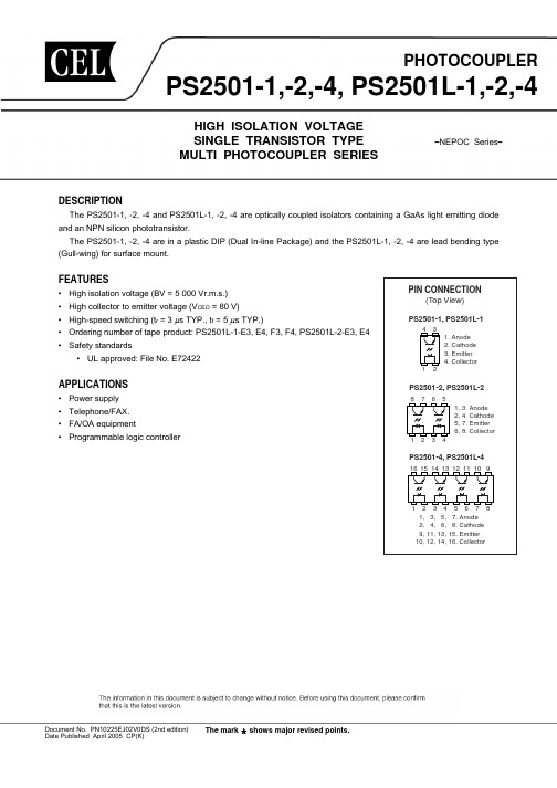
12
PS2501-2, PS2501L-2
8765 1234
1, 3. Anode 2, 4. Cathode 5, 7. Emitter 6, 8. Collector
PS2501-4, PS2501L-4
0.50±0.10
2.54
0.25 M
0
to 15˚ 0.25
+0.1 –0.05
2
Data Sheet PN10225EJ02V0DS
元器件交易网
Lead Bending Type (New package) PS2501L-1
4.6±0.35
PS2501-1,-2,-4, PS2501L-1,-2,-4
• UL approved: File No. E72422
APPLICATIONS
• Power supply • Telephone/FAX. • FA/OA equipment • Programmable logic controller
PIN CONNECTION (Top View)
PS2501-1, PS2501L-1
PS2501L-4
19.8±0.5
6.5±0.5
6.5±0.5
+0.1 –0.05
+0.1 –0.05
+0.1 –0.05
+0.1 –0.05
0.1
0.25
3.5±0.3
0.1
0.25
3.5±0.3
1.25±0.15 0.25 M 2.54
0.9±0.25 9.60±0.4 0.15
IRLML2502中文资料
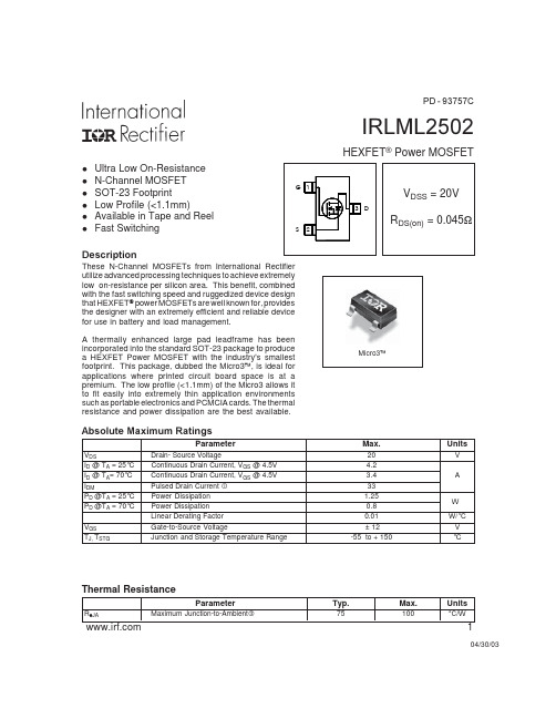
Min. Typ. Max. Units ––– ––– ––– ––– 16 8.6 1.3 A 33 1.2 24 13 V ns nC
Conditions MOSFET symbol showing the G integral reverse p-n junction diode. TJ = 25°C, IS = 1.3A, VGS = 0V TJ = 25°C, IF = 1.3A di/dt = 100A/µs
Fig 5. Typical Capacitance Vs. Drain-to-Source Voltage
Fig 6. Typical Gate Charge Vs. Gate-to-Source Voltage
100
1000
ISD , Reverse Drain Current (A)
OPERATION IN THIS AREA LIMITED BY RDS(on)
2.0
RDS(on) , Drain-to-Source On Resistance (Normalized)
ID = 4.0A
I D , Drain-to-Source Current (A)
1.5
TJ = 25 ° C
1.0
TJ = 150 ° C
0.5
10 2.0
V DS = 15V 20µs PULSE WIDTH 2.4 2.8 3.2 3.6 4.0
元器件交易网
PD - 93757C
IRLML2502
HEXFET® Power MOSFET
l l l l l l
Ultra Low On-Resistance N-Channel MOSFET SOT-23 Footprint Low Profile (<1.1mm) Available in Tape and Reel Fast Switching
DS2501中文资料
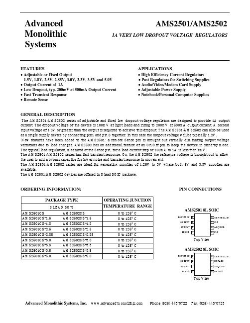
ORDERING INFORMATION:
PACKAGE TYPE
8 LEAD SO-8
AMS2501CS AMS2501CS-1.5 AMS2501CS-1.8 AMS2501CS-2.5 AMS2501CS-2.85 AMS2501CS-3.0 AMS2501CS-3.3 AMS2501CS-3.5 AMS2501CS-5.0
元器件交易网
Advanced Monolithic Systems
AMS2501/AMS2502
1A VERY LOW DROPOUT VOLTAGE REGULATORS
FEATURES
• Adjustable or Fixed Output 1.5V, 1.8V, 2.5V, 2.85V, 3.0V, 3.3V, 3.5V and 5.0V
1.485 1.500
1.515
V
AMS2501/AMS2502-1.8
VCONTROL = 4V, VPOWER =2.V, ILOAD = 0mA
1.782 1.800
1.818
V
VCONTROL = 3V, VPOWER =2.3V, ILOAD = 0mA to 1A
1.773 1.800
1.827
AMS2502CS AMS2502CS-1.5 AMS2502CS-1.8 AMS2502CS-2.5 AMS2502CS-2.85 AMS2502CS-3.0 AMS2502CS-3.3 AMS2502CS-3.5 AMS2502CS-5.0
OPERATING JUNCTION
TEMPERATURE RANGE
V
AMS2501/AMS2502-2.5
VCONTROL = 5V, VPOWER =3.3V, ILOAD = 0mA
长江连接器A2501系列
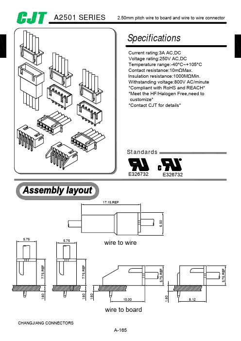
PART NO.
A2501H-2P A2501H-3P A2501H-4P A2501H-5P A2501H-6P A2501H-7P A2501H-8P A2501H-9P A2501H-10P A2501H-11P A2501H-12P A2501H-13P A2501H-14P A2501H-15P A2501H-16P A2501H-17P A2501H-18P A2501H-19P A2501H-20P
Standards
E326732
E326732
17.15.REF
5.75
5.75
wire to wire
7.75.REF
7.75.REF
5.75.REF
6.50
1.60
1.60
1.60
10.00
1.60
8.12
wire to board
CHANGJIANG CONNECTORS
A-165
5.75.REF
Part NO. A2501M-TB A2501M-TP A2501M-GB A2501M-GP Wire Range AWG#22-#28 AWG#22-#28 AWG#22-#28 AWG#22-#28 Insulation O.D. 1.00mm(max) 1.00mm(max) 1.00mm(max) 1.00mm(max) Material Brass Phosphor Bronze Brass Phosphor Bronze Finish Tin over Nickel Tin over Nickel Gold over Nickel Gold over Nickel
Dimensions A B
2.50 5.00 7.50 10.00 12.50 15.00 17.50 20.00 22.50 25.00 27.50 30.00 32.50 35.00 37.50 40.00 42.50 45.00 47.50 7.50 10.00 12.50 15.00 17.50 20.00 22.50 25.00 27.50 30.00 32.50 35.00 37.50 40.00 42.50 45.00 47.50 50.00 52.50 Unit: mm
74649-2501中文资料
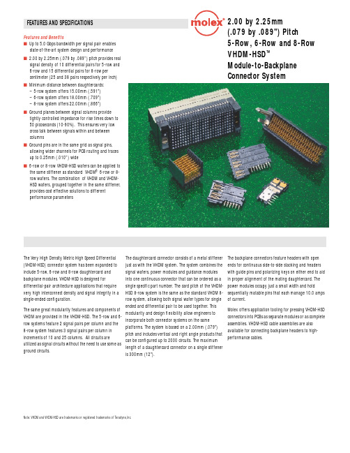
FEATURES AND SPECIFICATIONS2.00 by 2.25mm (.079 by .089") Pitch 5-Row, 6-Row and 8-Row VHDM-HSD ™Module-to-BackplaneConnector SystemFeatures and Benefitss Up to 5.0 Gbps bandwidth per signal pair enables state-of-the-art system design and performance s2.00 by 2.25mm (.079 by .089”) pitch provides real signal density of 10 differential pairs for 5-row and 6-row and 15 differential pairs for 8-row per centimeter (25 and 38 pairs respectively per inch) sMinimum distance between daughtercards:– 5-row system offers 15.00mm (.591")– 6-row system offers 18.00mm (.709")– 8-row system offers 22.00mm (.866")sGround planes between signal columns provide tightly controlled impedance for rise times down to 50 picoseconds (10-90%). This ensures very low cross talk between signals within and between columnssGround pins are in the same grid as signal pins, allowing wider channels for PCB routing and traces up to 0.25mm (.010”) wides6-row or 8-row VHDM-HSD wafers can be applied to the same stiffener as standard VHDM ® 6-row or 8-row wafers. The combination of VHDM and VHDM-HSD wafers, grouped together in the same stiffener, provides cost effective solutions to different performance parametersThe Very High Density Metric High Speed Differential (VHDM-HSD) connector system has been expanded to include 5-row, 6-row and 8-row daughtercard and backplane modules. VHDM-HSD is designed for differential-pair architecture applications that require very high interconnect density and signal integrity in a single-ended configuration.The same great modularity features and components ofVHDM are provided in the VHDM-HSD. The 5-row and 6-row systems feature 2 signal pairs per column and the8-row system features 3 signal pairs per column inincrements of 10 and 25 columns. All circuits areutilized as signal circuits without the need to use some asground circuits.The daughtercard connector consists of a metal stiffener just as with the VHDM system. The system combines the signal wafers, power modules and guidance modules into one continuous connector that can be ordered as a single specific part number. The card pitch of the VHDM-HSD 8-row system is the same as the standard VHDM 8-row system, allowing both signal wafer types for single ended and differential pair to be used together. Thismodularity and design flexibility allow engineers toincorporate both connector systems on the sameplatforms. The system is based on a 2.00mm (.079")pitch and includes vertical and right angle products thatcan be configured up to 2000 circuits. The maximumlength of a daughtercard connector on a single stiffeneris 300mm (12").The backplane connectors feature headers with open ends for continuous side-to-side stacking and headers with guide pins and polarizing keys on either end to aid in proper alignment of the mating daughtercard. The power modules occupy just a small width and hold sequentially matable pins that each manage 10.0 amps of current.Molex offers application tooling for pressing VHDM-HSD connectors into PCBs as separate modules or as complete assemblies. VHDM-HSD cable assemblies are also available for connecting backplane headers to high-performance cables.Note: VHDM and VHDM-HSD are trademarks or registered trademarks of Teradyne,Inc.元器件交易网FEATURES AND SPECIFICATIONS2.00 by 2.25mm (.079 by .089") Pitch 5-Row, 6-Row and 8-Row VHDM-HSD ™Module-to-Backplane Connector SystemPress Fit Right Angle ReceptacleApplicationsThe VHDM-HSD products are used in very high speed, short rise-time, high circuit count applications connecting daughtercards to the backplane:s Network Switches s Routerss Computer Serverss Telecommunication Equipment sInternetworking DevicesORDERING INFORMATIONDaughtercard AssemblyConfiguration 5-Row 6-Row 8-Row Signal wafers, power modules and guide modules sequentiallyassigned by application VHDM-HSD wafers74670-XXXX 74880-XXXX 74680-XXXX Combination of VHDM and VHDM-HSD wafers74686-XXXX 74886-XXXX74686-XXXXBackplane Header Signal Module Standard Loaded Pin Height 0.76µm (30µ”) Gold5-Row6-Row8-Row10-Column 25-Column 10-Column 25-Column 10-Column 25-Column Open Ended4.25mm (.167”)74695-100374695-250374979-100374979-250374649-100374649-25034.75mm (.187”)74695-100174695-250174979-100174979-250174649-100174649-25015.15mm (.203”)74695-100474695-250474979-100474979-250474649-100474649-25046.25mm (.266”)74695-100274695-250274979-100274979-250274649-100274649-2502Left Guide PinNo Polarizing Key 4.25mm (.167”)74696-100374696-2503––74650-100374650-25034.75mm (.187”)74696-100174696-2501––74650-100174650-25015.15mm (.203”)74696-100474696-2504––74650-100474650-25046.25mm (.266”)74696-100274696-2502––74650-100274650-2502Left Guide Pin“A” Polarizing Key 4.25mm (.167”)74696-101374696-2513––74650-101374650-25134.75mm (.187”)74696-101174696-2511––74650-101174650-25115.15mm (.203”)74696-101474696-2514––74650-101474650-25146.25mm (.266”)74696-101274696-2512––74650-101274650-2512Right Guide PinNo Polarizing Key 4.25mm (.167”)74697-100374697-2503––74651-100374651-25034.75mm (.187”)74697-100174697-2501––74651-100174651-25015.15mm (.203”)74697-100474697-2504––74651-100474651-25046.25mm (.266”)74697-100274697-2502––74651-100274651-2502Right Guide Pin“A” Polarizing Key 4.25mm (.167”)74697-101374697-2513––74651-101374651-25134.75mm (.187”)74697-101174697-2511––74651-101174651-25115.15mm (.203”)74697-101474697-2514––74651-101474651-25146.25mm (.266”)74697-101274697-2512––74651-101274651-2512Backplane Power and Guide Components5-Row and 6-Row 8-Row Power Module 74029-600074029-8000Keying Post 74069-001074069-0010Guide Pin74076-0001/000274076-0001/0002Americas Headquarters Lisle, Illinois 60532 U.S.A.1-800-78MOLEX amerinfo@ Far East North Headquarters Yamato, Kanagawa, Japan 81-462-65-2324feninfo@ Far East South Headquarters Jurong, Singapore 65-6-268-6868fesinfo@ European Headquarters Munich, Germany 49-89-413092-0eurinfo@ Corporate Headquarters 2222 Wellington Ct.Lisle, IL 60532 U.S.A.630-969-4550Visit our Web site at /product/backplan/hsd.htmlOrder No. USA-158 Rev. 2Printed in USA/2.5K/JI/JI/2003.03©2003, MolexNote: VHDM and VHDM-HSD are trademarks or registered trademarks of Teradyne,Inc.元器件交易网。
ps2501规格书
To our customers,Old Company Name in Catalogs and Other DocumentsOn April 1st, 2010, NEC Electronics Corporation merged with Renesas Technology Corporation, and Renesas Electronics Corporation took over all the business of both companies. Therefore, although the old company name remains in this document, it is a valid Renesas Electronics document. We appreciate your understanding.Renesas Electronics website: April 1st, 2010Renesas Electronics CorporationIssued by: Renesas Electronics Corporation ()Send any inquiries to /inquiry.Notice1. All information included in this document is current as of the date this document is issued. Such information, however, issubject to change without any prior notice. Before purchasing or using any Renesas Electronics products listed herein, please confirm the latest product information with a Renesas Electronics sales office. Also, please pay regular and careful attention to additional and different information to be disclosed by Renesas Electronics such as that disclosed through our website.2. Renesas Electronics does not assume any liability for infringement of patents, copyrights, or other intellectual property rightsof third parties by or arising from the use of Renesas Electronics products or technical information described in this document.No license, express, implied or otherwise, is granted hereby under any patents, copyrights or other intellectual property rights of Renesas Electronics or others.3. You should not alter, modify, copy, or otherwise misappropriate any Renesas Electronics product, whether in whole or in part.4. Descriptions of circuits, software and other related information in this document are provided only to illustrate the operation ofsemiconductor products and application examples. You are fully responsible for the incorporation of these circuits, software, and information in the design of your equipment. Renesas Electronics assumes no responsibility for any losses incurred by you or third parties arising from the use of these circuits, software, or information.5. When exporting the products or technology described in this document, you should comply with the applicable export controllaws and regulations and follow the procedures required by such laws and regulations. You should not use RenesasElectronics products or the technology described in this document for any purpose relating to military applications or use by the military, including but not limited to the development of weapons of mass destruction. Renesas Electronics products and technology may not be used for or incorporated into any products or systems whose manufacture, use, or sale is prohibited under any applicable domestic or foreign laws or regulations.6. Renesas Electronics has used reasonable care in preparing the information included in this document, but Renesas Electronicsdoes not warrant that such information is error free. Renesas Electronics assumes no liability whatsoever for any damages incurred by you resulting from errors in or omissions from the information included herein.7. Renesas Electronics products are classified according to the following three quality grades: “Standard”, “High Quality”, and“Specific”. The recommended applications for each Renesas Electronics product depends on the product’s quality grade, as indicated below. You must check the quality grade of each Renesas Electronics product before using it in a particularapplication. You may not use any Renesas Electronics product for any application categorized as “Specific” without the prior written consent of Renesas Electronics. Further, you may not use any Renesas Electronics product for any application for which it is not intended without the prior written consent of Renesas Electronics. Renesas Electronics shall not be in any way liable for any damages or losses incurred by you or third parties arising from the use of any Renesas Electronics product for an application categorized as “Specific” or for which the product is not intended where you have failed to obtain the prior written consent of Renesas Electronics. The quality grade of each Renesas Electronics product is “Standard” unless otherwiseexpressly specified in a Renesas Electronics data sheets or data books, etc.“Standard”: Computers; office equipment; communications equipment; test and measurement equipment; audio and visual equipment; home electronic appliances; machine tools; personal electronic equipment; and industrial robots.“High Quality”: Transportation equipment (automobiles, trains, ships, etc.); traffic control systems; anti-disaster systems; anti-crime systems; safety equipment; and medical equipment not specifically designed for life support.“Specific”: Aircraft; aerospace equipment; submersible repeaters; nuclear reactor control systems; medical equipment or systems for life support (e.g. artificial life support devices or systems), surgical implantations, or healthcareintervention (e.g. excision, etc.), and any other applications or purposes that pose a direct threat to human life.8. You should use the Renesas Electronics products described in this document within the range specified by Renesas Electronics,especially with respect to the maximum rating, operating supply voltage range, movement power voltage range, heat radiation characteristics, installation and other product characteristics. Renesas Electronics shall have no liability for malfunctions or damages arising out of the use of Renesas Electronics products beyond such specified ranges.9. Although Renesas Electronics endeavors to improve the quality and reliability of its products, semiconductor products havespecific characteristics such as the occurrence of failure at a certain rate and malfunctions under certain use conditions. Further, Renesas Electronics products are not subject to radiation resistance design. Please be sure to implement safety measures to guard them against the possibility of physical injury, and injury or damage caused by fire in the event of the failure of aRenesas Electronics product, such as safety design for hardware and software including but not limited to redundancy, fire control and malfunction prevention, appropriate treatment for aging degradation or any other appropriate measures. Because the evaluation of microcomputer software alone is very difficult, please evaluate the safety of the final products or system manufactured by you.10. Please contact a Renesas Electronics sales office for details as to environmental matters such as the environmentalcompatibility of each Renesas Electronics product. Please use Renesas Electronics products in compliance with all applicable laws and regulations that regulate the inclusion or use of controlled substances, including without limitation, the EU RoHS Directive. Renesas Electronics assumes no liability for damages or losses occurring as a result of your noncompliance with applicable laws and regulations.11. This document may not be reproduced or duplicated, in any form, in whole or in part, without prior written consent of RenesasElectronics.12. Please contact a Renesas Electronics sales office if you have any questions regarding the information contained in thisdocument or Renesas Electronics products, or if you have any other inquiries.(Note 1) “Renesas Electronics” as used in this document means Renesas Electronics Corporation and also includes its majority-owned subsidiaries.(Note 2) “Renesas Electronics product(s)” means any product developed or manufactured by or for Renesas Electronics.1988, 2010DATA SHEETThe information in this document is subject to change without notice. Before using this document, please confirm that this is the latest version.Not all products and/or types are available in every country. Please check with an NEC Electronics sales representative for availability and additional information.Document No. PN10225EJ05V0DS (5th edition)Date Published February 2010 NS Printed in JapanThe mark <R> shows major revised points.The revised points can be easily searched by copying an "<R>" in the PDF file and specifying it in the "Find what:" field.DESCRIPTIONThe PS2501-1, -4 and PS2501L-1, -4 are optically coupled isolators containing a GaAs light emitting diode and anNPN silicon phototransistor. The PS2501-1, -4 are in a plastic DIP (Dual In-line Package) and the PS2501L-1, -4 are lead bending type (Gull-wing) for surface mount.FEATURES• High isolation voltage (BV = 5 000 Vr.m.s.) • High collector to emitter voltage (V CEO = 80 V) • High-speed switching (t r = 3 μs TYP., t f = 5 μs TYP.)• Ordering number of tape product: PS2501L-1-F3: 2 000 pcs/reel • Safety standards • UL approved: No. E72422APPLICATIONS• Power supply • Telephone/AX. • A/OA equipment• Programmable logic controllerData Sheet PN10225EJ05V0DS2PACKAGE DIMENSIONS (UNIT : mm)DIP TypeLead Bending TypePHOTOCOUPLER CONSTRUCTIONParameter Unit (MIN.)Air Distance7 mm Outer Creepage Distance 7 mm Inner Creepage Distance 3.5 mm Isolation Distance0.3 mm<R>Data Sheet PN10225EJ05V0DS3MARKING EXAMPLE<R>Data Sheet PN10225EJ05V0DS4ORDERING INFORMATIONPart NumberOrder NumberSolder Plating SpecificationPacking StyleSafety StandardApproval Application Part Number *1PS2501-1 PS2501-1-A Pb-Free Magazine case 100 pcs Standard productsPS2501-1PS2501L-1 PS2501L-1-A(UL approved) PS2501L-1-F3 PS2501L-1-F3-A Embossed Tape 2 000 pcs/reelPS2501-4PS2501-4-AMagazine case 20 pcs PS2501-4 PS2501L-4 PS2501L-4-APS2501-1 PS2501-1Y-A Special version Magazine case 100 pcs Standard productsPS2501-1PS2501L-1 PS2501L-1Y-A (Pb-Free and (UL approved) PS2501L-1-F 3 PS2501L-1Y-F3-A Halogen Free)Embossed Tape 2 000 pcs/reel*1 For the application of the Safety Standard, following part number should be used.<R>Data Sheet PN10225EJ05V0DS5ABSOLUTE MAXIMUM RATINGS (Unless otherwise specified, T A = 25°C)RatingsParameter Symbol PS2501-1, PS2501L-1PS2501-4,PS2501L-4UnitDiode Reverse Voltage V R 6 V Forward Current (DC) I F 80 mA/chPower Dissipation DeratingΔP D /°C 1.5 1.2 mW/°CPower Dissipation P D 150 120 mW/chPeak Forward Current *1I FP 1 A/ch Transistor Collector to Emitter Voltage V CEO 80 VEmitter to Collector VoltageV ECO 7 V Collector Current I C 50 mA/chPower Dissipation DeratingΔP C /°C 1.5 1.2 mW/°CPower Dissipation P C 150120 mW/chIsolation Voltage *2BV 5 000 Vr.m.s. Operating Ambient Temperature T A −55 to +100 °C Storage TemperatureT stg−55 to +150°C*1 PW = 100 μs, Duty Cycle = 1%*2 AC voltage for 1 minute at T A = 25°C, RH = 60% between input and output. Pins 1-2 shorted together, 3-4 shorted together (PS2501-1, PS2501L-1). Pins 1-8 shorted together, 9-16 shorted together (PS2501-4, PS2501L-4).Data Sheet PN10225EJ05V0DS6ELECTRICAL CHARACTERISTICS (T A = 25°C)Parameter Symbol Conditions MIN. TYP. MAX. UnitDiode Forward VoltageV FI F = 10 mA 1.17 1.4 VReverse Current I R V R = 5 V5 μATerminal Capacitance C t V = 0 V, f = 1.0 MHz 50pF Transistor Collector to Emitter DarkCurrentI CEOV CE = 80 V, I F = 0 mA100nACoupledCurrent Transfer Ratio (I C /I F )*1CTR I F = 5 mA, V CE = 5 V 80 300 600 %Collector Saturation VoltageV CE (sat)I F = 10 mA, I C = 2 mA0.3 VIsolation Resistance R I-O V I-O = 1.0 kV DC 1011Ω Isolation Capacitance C I-O V = 0 V, f = 1.0 MHz0.5pFRise Time *2t r V CC = 10 V, I C = 2 mA, R L = 100 Ω 3 μsFall Time *2t f5*1 CTR rank ( * : only PS2501-1, PS2501L-1) K* : 300 to 600 (%) L* : 200 to 400 (%) M* : 80 to 240 (%) D* : 100 to 300 (%) H* : 80 to 160 (%) W* : 130 to 260 (%) Q* : 100 to 200 (%)N : 80 to 600 (%)*2 Test circuit for switching timeV CCOUTΩInputOutput<R>Data Sheet PN10225EJ05V0DS7TYPICAL CHARACTERISTICS (Unless otherwise specified, T A = 25°C)150100500255075125150150502550100125150D i o d e P o w e r D i s s i p a t i o n P D (m W )T r a n s i s t o r P o w e r D i s s i p a t i o n P C (m W )Ambient Temperature T A (°C)F o r w a r d C u r r e n t I F (m A )Forward Voltage V F (V)C o l l e c t o r t oE m i t t e r D a r k C u r r e n t I C E O (n A )Collector Saturation Voltage V CE (sat) (V)Ambient Temperature T A (°C)Ambient Temperature T A (°C)DIODE POWER DISSIPATION vs.AMBIENT TEMPERATURE TRANSISTOR POWER DISSIPATION vs. AMBIENT TEMPERATUREFORWARD CURRENT vs.FORWARD VOLTAGECOLLECTOR TO EMITTER DARKCURRENT vs. AMBIENT TEMPERATURECOLLECTOR CURRENT vs.COLLECTOR SATURATION VOLTAGEC o l l e c t o r C u r r e n t I C (m A )26C o l l e c t o r C u r r e n t I C (m A )Collector to Emitter Voltage V CE (V)COLLECTOR CURRENT vs.COLLECTOR TO EMITTER VOLTAGERemark The graphs indicate nominal characteristics.Data Sheet PN10225EJ05V0DS8Load Resistance R L (Ω)Frequency f (kHz)N o r m a l i z e d C u r r e n t T r a n s f e r R a t i o C T RC u r r e n t T r a n s f e r R a t i o C T R (%)N o r m a l i z e d G a i n G VS w i t c h i n g T i m e t ( s )μNORMALIZED CURRENT TRANSFER RATIO vs. AMBIENT TEMPERATURECURRENT TRANSFER RATIO vs.FORWARD CURRENTFREQUENCY RESPONSES w i t c h i n g T i m e t ( s )μ400350300250200150100500101010Time (Hr)C T R (R e l a t i v e V a l u e )Remark The graphs indicate nominal characteristics.TAPING SPECIFICATIONS (UNIT : mm)Data Sheet PN10225EJ05V0DS 9Data Sheet PN10225EJ05V0DS10NOTES ON HANDLING1. Recommended soldering conditions(1) Infrared reflow soldering • Peak reflow temperature 260°C or below (package surface temperature) • Time of peak reflow temperature 10 seconds or less • Time of temperature higher than 220°C 60 seconds or less • Time to preheat temperature from 120 to 180°C 120±30 s• Number of reflows Three• Flux Rosin flux containing small amount of chlorine (The flux with a maximum chlorine content of 0.2 Wt% is recommended.)P a c k a g e S u r f a c e T e m p e r a t u r e T (°C )Time (s)Recommended Temperature Profile of Infrared Reflow(2) Wave soldering • Temperature 260°C or below (molten solder temperature) • Time10 seconds or less• Preheating conditions 120°C or below (package surface temperature)• Number of times One (Allowed to be dipped in solder including plastic mold portion.)• Flux Rosin flux containing small amount of chlorine (The flux with a maximum chlorine content of 0.2 Wt% is recommended.)(3) Soldering by soldering iron• Peak temperature (lead part temperature) 350°C or below • Time (each pins)3 seconds or less• Flux Rosin flux containing small amount of chlorine (The flux with a maximum chlorine content of 0.2 Wt% is recommended.)(a) Soldering of leads should be made at the point 1.5 to 2.0 mm from the root of the lead. (b) Please be sure that the temperature of the package would not be heated over 100°C.(4) Cautions• FluxesAvoid removing the residual flux with freon-based and chlorine-based cleaning solvent.2. Cautions regarding noiseBe aware that when voltage is applied suddenly between the photocoupler’s input and output or between collector-emitters at startup, the output transistor may enter the on state, even if the voltage is within the absolute maximum ratings.3. Measurement conditions of current transfer ratios (CTR), which differ according to photocouplerCheck the setting values before use, since the forward current conditions at CTR measurement differ according to product.When using products other than at the specified forward current, the characteristics curves may differ from the standard curves due to CTR value variations or the like. This tendency may sometimes be obvious, especially below I F = 1 mA.Therefore, check the characteristics under the actual operating conditions and thoroughly take variations or the like into consideration before use.USAGE CAUTIONS1.Protect against static electricity when handling.2.Avoid storage at a high temperature and high humidity.Data Sheet PN10225EJ05V0DS 11Data Sheet PN10225EJ05V0DS12The information in this document is current as of February, 2010. The information is subject to change without notice. For actual design-in, refer to the latest publications of NEC Electronics data sheets, etc., for the most up-to-date specifications of NEC Electronics products. Not all products and/or types are available in every country. Please check with an NEC Electronics sales representative for availability and additional information.No part of this document may be copied or reproduced in any form or by any means without the prior written consent of NEC Electronics. NEC Electronics assumes no responsibility for any errors that may appear in this document.NEC Electronics does not assume any liability for infringement of patents, copyrights or other intellectual property rights of third parties by or arising from the use of NEC Electronics products listed in this document or any other liability arising from the use of such products. No license, express, implied or otherwise, is granted under any patents, copyrights or other intellectual property rights of NEC Electronics or others.Descriptions of circuits, software and other related information in this document are provided for illustrative purposes in semiconductor product operation and application examples. The incorporation of these circuits, software and information in the design of a customer's equipment shall be done under the full responsibility of the customer. NEC Electronics assumes no responsibility for any losses incurred by customers or third parties arising from the use of these circuits, software and information.While NEC Electronics endeavors to enhance the quality and safety of NEC Electronics products, customers agree and acknowledge that the possibility of defects thereof cannot be eliminated entirely. In addition, NEC Electronics products are not taken measures to prevent radioactive rays in the product design. When customers use NEC Electronics products with their products, customers shall, on their own responsibility, incorporate sufficient safety measures such as redundancy, fire-containment and anti-failure features to their products in order to avoid risks of the damages to property (including public or social property) or injury (including death) to persons, as the result of defects of NEC Electronics products.NEC Electronics products are classified into the following three quality grades: "Standard", "Special" and "Specific".The "Specific" quality grade applies only to NEC Electronics products developed based on a customer-designated "quality assurance program" for a specific application. The recommended applications of an NEC Electronics product depend on its quality grade, as indicated below. Customers must check the quality grade of each NEC Electronics product before using it in a particular application.The quality grade of NEC Electronics products is "Standard" unless otherwise expressly specified in NEC Electronics data sheets or data books, etc. If customers wish to use NEC Electronics products in applications not intended by NEC Electronics, they must contact an NEC Electronics sales representative in advance to determine NEC Electronics' willingness to support a given application.(Note)••••••M8E0904E(1)(2)"NEC Electronics" as used in this statement means NEC Electronics Corporation and also includes itsmajority-owned subsidiaries."NEC Electronics products" means any product developed or manufactured by or for NEC Electronics (asdefined above).Computers, office equipment, communications equipment, test and measurement equipment, audioand visual equipment, home electronic appliances, machine tools, personal electronic equipment and industrial robots.Transportation equipment (automobiles, trains, ships, etc.), traffic control systems, anti-disastersystems, anti-crime systems, safety equipment and medical equipment (not specifically designed for life support).Aircraft, aerospace equipment, submersible repeaters, nuclear reactor control systems, lifesupport systems and medical equipment for life support, etc."Standard":"Special":"Specific":。
LM2501SL资料
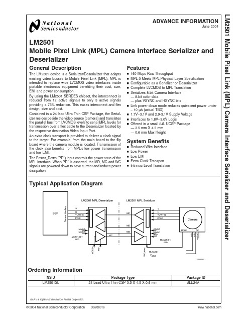
LM2501Mobile Pixel Link (MPL)Camera Interface Serializer and DeserializerGeneral DescriptionThe LM2501device is a Serializer/Deserializer that adapts existing video busses to Mobile Pixel Link (MPL).MPL is intended to replace wide LVCMOS video interfaces inside portable electronics equipment benefiting their cost,size,EMI and power consumption.By using the LM2501SERDES chipset,the interconnect is reduced from 12active signals to only 3active signals providing a 75%reduction.This eases interconect and flex design,size and cost.Contained in a 24lead Ultra Thin CSP Package,the Serial-izer resides beside the video source (camera)and translates the parallel bus from LVCMOS levels to serial MPL levels for transmission over a flex cable to the Deserializer located by the respective destination Video Input Port.An extra clock transport is provided to deliver a clock signal to the target.For example,from the main board to the flip board where the camera module is located.Transmission of the clock also benefits from MPL’s low power transmission and low EMI.The Power_Down (PD*)input controls the power state of the MPL interface.When PD*is asserted,the MD,MC and WC signals are powered down to save current and reduce power dissipation.Featuresn 160Mbps Raw Throughputn MPL-0Meets MPL Physical Layer Specification n Configurable as a Serializer or Deserializer n Complete LVCMOS to MPL Translation nSerializes 8-bit Camera Interface —8-bit color data—plus VSYNC and HSYNC bitsn Link power down mode reduces quiescent power under ∼10µA (actual TBD)n 1.7V–3.1V and 2.9-3.1V Supply Voltage n Interfaces to 1.8V–3.0V LogicnOffered in a small 24L UCSP Package —3.5mm X 4.5mm —0.6mm Max HeightSystem Benefitsn Reduced Wire Interface n Low Power n Low EMIn Extra Clock Transport nIntrinsic Level TranslationTypical Application Diagram20091601Ordering InformationNSID Package TypePackage ID LM2501SL24-Lead Ultra Thin CSP 3.5X 4.5X 0.6mmSLE24AI2C ®is a registered trademark of Phillips Corporation.ADVANCE INFORMATIONJune 2004LM2501Mobile Pixel Link (MPL)Camera Interface Serializer and Deserializer©2004National Semiconductor Corporation Connection Diagram20091612TOP VIEWGeneral Block Diagrams:Serializer and Deserializer20091613L M 2501 2Pin DescriptionPin NameNo.of PinsI/O,Type DescriptionMPL SERIAL BUS PINSMD1IO,MPL MPL Data line.Serializer is a Line Driver.Deserializer is a Receiver.Configured bythe Mode[1:0]pins.MC1IO,MPL MPL Clock line.Serializer is a Line Driver.Deserializer is a Receiver.Configured bythe Mode[1:0]pins.MG1Ground See VSSA below.CONFIGURATION/PARALLEL BUS PINSMode[1:0]2I,LVCMOS Mode Configuration Input pins:Mode[1:0],NOTE-Applies to REV F/G Samples only.00:Deserializer01:Serializer with PD*input10:Reserved11:ReservedPD*1I,LVCMOS Power_Down.Input pin.Active Low.When PD*is Low the device is in the sleepstate.D0–D78IO,LVCMOS8-bit Bi-directional Data Bus–Serializer Input,Deserializer OutputVS1IO,LVCMOS VSYNC–Serializer Input,Deserializer OutputHS1IO,LVCMOS HSYNC–Serializer Input,Deserializer OutputPCLK1IO,LVCMOS Pixel Clock.Serializer Input,Deserializer OutputWHISPER CLOCKWCLKIO1IO,LVCMOS Extra Clock Input for WhisperClock Link–Deserializer Input.Serializer Output.WC1IO,MPL Extra WhisperClock MPL signal–Serializer is an MPL input signal,Deserializer isan MPL output signal.POWER/GROUND PINSV DDA1Power Power Supply Pin for the MPL Interface.3.0V±3%V SSA1Ground Ground Pin for the MPL Interface,also known as MG(MPL Ground)V DD1Power Power Supply Pin for the digital core and Serializer PLL.3.0V±3%V SS1Ground Ground Pin for the digital core and Serializer PLL.V DDIO1Power Power Supply Pin for the parallel interface.1.7V to3.1VV SSIO1Ground Ground Pin for the parallel interface.Notes:I=Input,O=Output,IO=Input/OutputDo NOT float unused inputs.ES Revision notesRev D/E Sampled on MPL200EVK Use prior datasheet editionRev F S/D*and TM pins changed to Mode[1:0]Use this datasheet editionRev G MPL RX enhancementsLM25013Absolute Maximum Ratings (Note 1)If Military/Aerospace specified devices are required,please contact the National Semiconductor Sales Office/Distributors for availability and specifications.Supply Voltage (V DDA )−0.3V to +TBDV Supply Voltage (V DD )−0.3V to +TBDV Supply Voltage (V DDIO )−0.3V to +TBDV LVCMOS Input/Output Voltage −0.3V to (V DDIO+0.3V)MPL Input/Output Voltage TBD Junction Temperature +150˚CStorage Temperature −65˚C to +150˚CLead Temperature Soldering,4Seconds +260˚CESD Ratings:HBM,1.5k Ω,100pF≥±2kVEIAJ,0Ω,200pF ≥±200V Maximum Package Power Dissipation Capacity at 25˚C24L UCSP PackageTBD W Derate TBD Package above 25˚CTBD mW/˚CRecommended Operating ConditionsMin Typ MaxUnitsSupply Voltage V DDA to V SSA and V DD to V SS 2.9 3.03.1V V DDIO to V SSIO 1.7 3.1V PLK Clock Frequency 416MHz WC Clock Frequency 428MHz Ambient Temperature2570˚C Electrical CharacteristicsOver recommended operating supply and temperature ranges unless otherwise specified.(Note 2)Symbol ParameterConditionsMinTypMaxUnitsMPL I OLL Logic Low Current 4.8I B5.0I B 5.3I BµA I OMS Mid Scale Current 3.0I B µA I OHL Logic High Current 0.8I B 1.0I B 1.2I B µA I B Current Bias150µALVCMOS (1.7V to 3.1V)V IH Input Voltage High Level 0.7V DDIOV DDIO +0.3V V IL Input Voltage Low Level −0.30.3V DDIOV I IN Input Current (includes I OZ )−50+5µA I IH Input Current High Level −10+1µA I IL Input Current Low Level −10+1µA V OH Output Voltage High Level I OH =−2mA 0.8V DDIOV V OL Output Voltage Low Level I OL =2mA 0.2V DDIO V I OSOutput Short Circuit CurrentV OUT =0VTBDmASUPPLY CURRENT I CCTotal SupplyCurrent —EnabledPCLK =16MHz WC =28MHz MD =0101-1010pattern C L =15pFSerializerTBDTBDµADeserializerTBD TBD µA I CCZSupply Current —Disable Power_Down Mode PD*=L110µA PD*=L110µAL M 2501 4Switching CharacteristicsOver recommended operating supply and temperature ranges unless otherwise specified.(Note2)Symbol Parameter Conditions Min Typ Max Units PARALLEL BUS TIMINGt SET Set Time-Data to Clock Inputs Figure2TBD ns t HOLD Hold Time-Clock to Data TBD nst RISE Rise Time Outputs,C L=15pF nst FALL Fall Time ns PC LOW PCLK Low50% PC HIGH PCLK High50% t DVBC Data Valid before Clock Figure2TBD ns t DVAC Data Valid after Clock TBD ns SERIAL BUS TIMINGt DVBC Figure1t DVACPOWER UP TIMING(see Figures5,6)t1WC Start Up Delay Figure5Planned Rev G ES test Chip willdouble WC cyc counts on T1to T4(SER)parameters to support higherWC rates.100WC CYCt2WC Low Initialization LowState111213WC CYC t3WC Pulse Width High111213WC CYC t4WC Low State111213WC CYC t5WC IN to WC OUT Latency(SER)678WC CYC t6TBD9WC CYC t7SER PLL Lock Time Figure64,096MC CYC t8MC Low Initialization LowState111213MC CYC t9MC Pulse Width High111213MC CYC t10MC Low State111213MC CYC t11SER Latency TBD MC CYC t12DES Latency TBD MC CYC POWER OFF TIMINGt PAZ Disable Time to Power Offµst PZA Enable Time from PowerOffµsLM25015Input Timing RequirementsOver recommended operating supply and temperature ranges unless otherwise specified.(Note 2)Symbol ParameterConditionsMin TypMax Units REFERENCE CLOCK (WCLK IN )f WC Clock Frequency 428MHz WC DC Clock Duty Cycle 455055%t TClock Transition Times (Rise or Fall,10%–90%)16nsPIXEL CLOCK (PCLK)f PCLK Clock Frequency 416MHz t CP Clock Period 62.5250ns CLK DC Clock Duty Cycle 455055%t TClock transition Time16nsNote 1:“Absolute Maximum Ratings“are those values beyond which the safety of the device cannot be guaranteed.They are not meant to imply that the device should be operated at these limits.The tables of “Electrical Characteristics”specify conditions for device operation.Note 2:Typical values are given for V DD =V DDA =3.0V and V DDIO =2.7V and T A =25˚C.Note 3:Current into a device pin is defined as positive.Current out of device pins is defined as negative.Voltages are referenced to Ground unless otherwise specified.Timing Diagrams20091610FIGURE 1.Serial Data Valid20091611FIGURE 2.Parallel Set,Hold and Data ValidL M 2501 6Application InformationTypical application connections for the LM2501are shown below.The application shown in Figure 3illustrates a connection between an Image sensor and a host utilizing an MPL-0link..20091614FIGURE 3.Camera ApplicationLM25017Functional DescriptionSERIAL BUS OPERATION Bus OverviewThe MPL bus is a simple 2-signal line interface that is intended to replace wide low voltage CMOS video busses inside handheld portable devices.The MPL physical layer is purpose-built for an extremely low power and low EMI data transmission while requiring the fewest number of signal lines.No external line components are required,as termina-tion is provided internal to the MPL receiver.The MPL inter-face is designed to be used with common 50Ωlines using standard materials and connectors.Lines may be microstrip or stripline construction.Total length of the interconnect is expected to be less than 0.3meters.This device is meets the requirements of the MPL-0Standard (PHY Layer only).SERIAL BUS TIMINGData valid is relative to both edges as shown in Figure 4.Data valid is specified as:Data Valid before Clock,Data Valid after Clock,(Note relative to both edges).SERIAL BUS PHASESThere are three bus phases on the MPL serial bus.These are determined by the state of the MC and MD lines.Two of the bus phases have options.The MPL bus phases are shown in Table 1.TABLE 1.MPL Bus PhasesNameWC StateMC StateMD StatePhase Description Pre-PhasePost-Phase OFF (O)000Bus is Powered-Off na I (WC)Initialization (I)WC A 00WC Start Up O I (MC)MC/MDA A 0MPL Start Up I (WC)A Active (A)AAXData Out (Write)I (MC)A or ONotes on Line State:0=no current (off),L =Logic Low,H =Logic High,X =Low or High,A —Active Clock20091602FIGURE 4.Master-to-Slave Timing (MC,MDm)L M 2501 8Functional Description(Continued)SERIAL BUS POWER-UPIn the sleep state,WC,MC and MD are turned off with zero current flowing.Both devices need to be enabled by assert-ing their PD*inputs.The DES will then initialize the SER via the WC signal as shown in Figure5.The DES waits7WC cycles before its WCLK out is active.Note,there is no phase or frequency relationship between WC and MC.20091603FIGURE5.Bus Power Up Timing—WCLM25019Functional Description(Continued)In Figure 6,the Serializer timing is shown.For the part to establish lock,WCLKIO(out)must be active,and a valid PCLK applied.After lock is obtained,the MC and MD lines are initialized and then active transmission occurs.Table Switching Characteristics lists the timing parameters of Fig-ures 5,6.SERIAL BUS POWER-OFFIn the power-off state,WC,MD and MC are turned off with zero current flowing.This is considered the Sleep state (Power-off)and the transition off may occur after the last data bit time or at any time afterwards from an Idle phase as shown in Figure 7.20091604FIGURE 6.Bus Power Up Timing —MC/MD20091605FIGURE 7.Bus Power Down TimingL M 2501 10Functional Description(Continued)CAMERA INTERFACEThe Camera Interface provides serialization of color and control bits.The interface provides data transport in a single direction.Byte alignment is provided by the intrinsic firstrising edge of the MC line.PCLK is required and must be free-running .Data may be raw Bayer or BT656color infor-mation.Data is strobed on the rising-edge on the input to the Serializer.Data is sent LSB first (D0).MPL provides the data transport path,control of the Camera device is provided by an I 2C control bus.20091606FIGURE 8.Camera Mode Serial Interface20091607FIGURE 9.Parallel Bus TimingLM250111Features and OperationPOWER DOWN/OFFThe device may be powered by its PD*pin.A Low on this pin will power down the entire device.TABLE 2.Power Down Output StatesMode Pin Type Output State in Power DownSER WCLKIO LVCMOS LOW SER MC MPL OFF SER MD MPL OFF DES D[0:7]LVCMOS LOW DES V,H LVCMOS LOW DES PCLK LVCMOS LOW DESWCMPLOFFUN-USED/OPEN INPUTSUn-used control/inputs pins must be driven to their appropri-ate logic states to set up the desired operating modes.UN-USED OUTPUTSUnused outputs should be left open to minimize power dis-sipation.POWERING UPThe LM2501should be powered up with all power supplies at the same time,alternately VDDIO may lag VDD and VDDA.Do not power up with VDDIO before VDD and VDDA.PHASE-LOCKED LOOPWhen the device is configured as a Serializer,a PLL is provided to generate the serial link clock.The Phase-locked loop system generates the serial data clock at five times the input clock.The PLL operates with an input clock between 4MHz and 16MHz.The Deserializer does not utilize the PLL and its PLL is powered down.RESETPD*should be held Low until the power supply has powered up and is stable.The PD*should then be de-asserted to generate a RESET and start up.Stopping the WCLKIO or the PCLK will not RESET the part.A power cycle or PD*cycle is requested to generate a RESET event.SERIALIZER/DESERIALIZER SELECTIONThe Mode[1:0]pins are used to configure the device as either a Serializer or Deserializer and other configuration options.WHISPERCLOCKAn additional clock signal is sent from the Deserializer to the Serializer.This can be used to pass a clock reference (4MHz to 28MHz)up to the Camera device from the host.This link is independent of the Serial data path (opposite direction).See also Figure 5.The SER can only start up,if the WCLKIO(ser-out)has been active.20091608FIGURE 10.Sleep to ActiveL M 2501 12Features and Operation(Continued) When the Deserializer’s PD*signal is de-asserted,the WC output will power up and initialize the serializer and start transmitting the clock reference.Once the Serializer re-ceived the clock,it waits seven cycles,and then outputs the clock signal.Seven cycles later,the Serializer’s PLL will begin to lock if PCLK is present.When the Deserializer’s PD*signal is asserted,the WC signal is turned off.MISC.Definitions:Bus States:Logic Low—5Idata flowing from the Receiver to theDriverLogic High—Idata flowing from the Receiver to the Driver Power Off—No Current flowing in the interconnect Signals&Nomenclature:MD=MPL Data Signal,subscript denotes source,m= master,s=slaveMC=MPL Clock SignalWC=MPL WhisperClock Signal*=Active Low Signal20091609FIGURE11.Active to SleepLM2501 13Physical Dimensionsinches (millimeters)unless otherwise notedOrder Number LM2501SL NS Package Number SLE24ALIFE SUPPORT POLICYNATIONAL’S PRODUCTS ARE NOT AUTHORIZED FOR USE AS CRITICAL COMPONENTS IN LIFE SUPPORT DEVICES OR SYSTEMS WITHOUT THE EXPRESS WRITTEN APPROVAL OF THE PRESIDENT AND GENERAL COUNSEL OF NATIONAL SEMICONDUCTOR CORPORATION.As used herein:1.Life support devices or systems are devices or systems which,(a)are intended for surgical implant into the body,or (b)support or sustain life,and whose failure to perform when properly used in accordance with instructions for use provided in the labeling,can be reasonably expected to result in a significant injury to the user. 2.A critical component is any component of a life support device or system whose failure to perform can be reasonably expected to cause the failure of the life support device or system,or to affect its safety or effectiveness.BANNED SUBSTANCE COMPLIANCENational Semiconductor certifies that the products and packing materials meet the provisions of the Customer Products Stewardship Specification (CSP-9-111C2)and the Banned Substances and Materials of Interest Specification (CSP-9-111S2)and contain no ‘‘Banned Substances’’as defined in CSP-9-111S2.National Semiconductor Americas Customer Support CenterEmail:new.feedback@ Tel:1-800-272-9959National SemiconductorEurope Customer Support CenterFax:+49(0)180-5308586Email:europe.support@Deutsch Tel:+49(0)6995086208English Tel:+44(0)8702402171Français Tel:+33(0)141918790National Semiconductor Asia Pacific Customer Support CenterEmail:ap.support@National SemiconductorJapan Customer Support Center Fax:81-3-5639-7507Email:jpn.feedback@ Tel:81-3-5639-7560L M 2501M o b i l e P i x e l L i n k (M P L )C a m e r a I n t e r f a c e S e r i a l i z e r a n d D e s e r i a l i z e rNational does not assume any responsibility for use of any circuitry described,no circuit patent licenses are implied and National reserves the right at any time without notice to change said circuitry and specifications.。
1945122资料

Address
PHOENIX CONTACT GmbH & Co. KG Flachsmarktstr. 8 32825 Blomberg,Germany Phone +49 5235 3 00 Fax +49 5235 3 41200 http://www.phoenixcontact.de
Dimensioned drawing
PHOENIX CONTACT GmbH & Co. KG http://www.phoenixcontact.de
Page 3 / 4 Apr 12, 2008
元器件交易网
PST 1,0/ 5-3,5 Order No.: 1945122
元器件交易网
Extract from the online catalog
PST 1,0/ 5-3,5
Order No.: 1945122
The figure shows a 10-position version of the product
http://eshop.phoenixcontact.de/phoenix/treeViewClick.do?UID=1945122
Technical data Dimensions / positions Pitch Dimension a Number of positions Pin dimensions Hole diameter 3.5 mm 14 mm 5 1 mm 1.1 mm
PHOENIX CONTACT GmbH & Co. KG http://www.phoenixcontact.de
PS2501-1X中文资料

SURFACE MOUNT OPTION G
PS2501-4X PS2501-4
2.54 7.0 6.0 1.2 20.32 19.32 4.0 3.0 0.5 3.0 0.5 3.35 0.26 7.62 13° Max
7.62
0.6 0.1 10.46 9.86
1.25 0.75
Collector-emitter Saturation Voltage vs. Forward Current =1mA 3mA 5mA 10mA 15mA
150
100
50
0 -30 0 25 50 75 100 125 Ambient temperature TA ( °C ) Forward Current vs. Ambient Temperature 60
DB92402m-AAS/A4
Collector-emitter saturation voltage VCE(SAT) (V)
VCE = 5V TA = 25°C
4/2/03
80V 6V 150mW
200mW
ELECTRICAL CHARACTERISTICS ( TA = 25°C Unless otherwise noted ) PARAMETER Input Forward Voltage (VF) Reverse Current (IR) Output Collector-emitter Breakdown (BVCEO) 80 ( Note 2 ) Emitter-collector Breakdown (BVECO) 6 Collector-emitter Dark Current (ICEO) Current Transfer Ratio (CTR) (Note 2) PS2501-1,PS2501-2,PS2501-4
PS2501-1
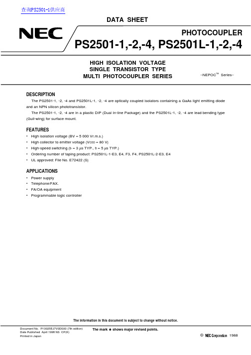
DATA SHEETThe information in this document is subject to change without notice.©1988Document No. P10025EJ7V0DS00 (7th edition)Date Published April 1998 NS CP(K)Printed in JapanThe mark • shows major revised points.DESCRIPTIONThe PS2501-1, -2, -4 and PS2501L-1, -2, -4 are optically coupled isolators containing a GaAs light emitting diode and an NPN silicon phototransistor.The PS2501-1, -2, -4 are in a plastic DIP (Dual In-line Package) and the PS2501L-1, -2, -4 are lead bending type (Gull-wing) for surface mount.FEATURES•High isolation voltage (BV = 5 000 Vr.m.s.)•High collector to emitter voltage (V CEO = 80 V)•High-speed switching (t r = 3 µs TYP., t f = 5 µs TYP.)•Ordering number of taping product: PS2501L-1-E3, E4, F3, F4, PS2501L-2-E3, E4•UL approved: File No. E72422 (S)APPLICATIONS•Power supply •Telephone/FAX.•FA/OA equipment•Programmable logic controller查询PS2501-1供应商PACKAGE DIMENSIONS (in millimeters) DIP TypeCaution New package 1-ch, 4-ch only2Lead Bending TypeCaution New package 1-ch, 4-ch only34ABSOLUTE MAXIMUM RATINGS (T A = 25 °C, unless otherwise specified)RatingsParameterSymbolPS2501-1,PS2501L-1PS2501-2,-4PS2501L-2,-4UnitDiode Reverse Voltage V R 6V Forward Current (DC)I F80mA Power Dissipation Derating ∆P D /°C 1.5 1.2mW/°C Power Dissipation P D 150120mW/ch Peak Forward Current*1I FP 1A Transistor Collector to Emitter Voltage V CEO 80V Emitter to Collector Voltage V ECO 7V Collector CurrentI C50mA/ch Power Dissipation Derating ∆P C /°C 1.5 1.2mW/°C Power DissipationP C 150120mW/ch Isolation Voltage*2BV 5 000Vr.m.s.Operating Ambient Temperature T A −55 to +100°C Storage TemperatureT stg−55 to +150°C*1PW = 100 µs, Duty Cycle = 1 %*2AC voltage for 1 minute at T A = 25 °C, RH = 60 % between input and output5ELECTRICAL CHARACTERISTICS (T A = 25 °C)ParameterSymbol Conditions MIN.TYP.MAX.Unit DiodeForward Voltage V F I F = 10 mA 1.171.4VReverse Current I R V R = 5 V5µA Terminal CapacitanceC t V = 0 V, f = 1.0 MHz 50pFTransistorCollector to Emitter Dark CurrentI CEOV CE = 80 V, I F = 0 mA100nACoupled Current Transfer Ratio(I C /I F )*1CTR I F = 5 mA, V CE = 5 V 80300600%Collector Saturation VoltageV CE (sat)I F = 10 mA, I C = 2 mA0.3V Isolation Resistance R I-O V I-O = 1.0 kV DC1011ΩIsolation Capacitance C I-O V = 0 V, f = 1.0 MHz0.5pFRise Time *2t r V CC = 10 V, I C = 2 mA, R L = 100 Ω3µsFall Time*2t f5*1CTR rank ( * : only PS2501-1, PS2501L-1)*2Test circuit for switching timeK*: 300 to 600 (%)L*: 200 to 400 (%)M*: 80 to 240 (%)D*: 100 to 300 (%)H*: 80 to 160 (%)W*: 130 to 260 (%)Q*: 100 to 200 (%)N : 80 to 600 (%)V CCOUTΩ6TYPICAL CHARACTERISTICS (T A = 25 °C, unless otherwise specified)15010050025507512515025501001251501D i o d e P o w e r D i s s i p a t i o n P D (m W )T r a n s i s t o r P o w e r D i s s i p a t i o n P C (m W )Ambient Temperature T A (˚C)F o r w a r d C u r r e n t I F (m A )Forward Voltage V F (V)C o l l e c t o r t o E m i tt e r D a r k C u r r e n t I C E O (n A )Collector Saturation Voltage V CE(sat) (V)Ambient Temperature T A (˚C)Ambient Temperature T A (˚C)DIODE POWER DISSIPATION vs.AMBIENT TEMPERATURETRANSISTOR POWER DISSIPATION vs. AMBIENT TEMPERATUREFORWARD CURRENT vs.FORWARD VOLTAGECOLLECTOR TO EMITTER DARKCURRENT vs. AMBIENT TEMPERATURECOLLECTOR CURRENT vs.COLLECTOR SATURATION VOLTAGEC o l l e c t o r C u r r e n t I C (m A )75C o l l e c t o r C u r r e n t I C (m A )Collector to Emitter Voltage V CE (V)COLLECTOR CURRENT vs.COLLECTOR TO EMITTER VOLTAGE7Load Resistance R L (Ω)Frequency f (kHz)N o r m a l i z e d C u r r e n t T r a n s f e r R a t i o C T RC u r r e n t T r a n s f e r R a t i o C T R (%)N o r m a l i z e d G a i n G VS w i t c h i n g T i m e t ( s )µNORMALIZED CURRENT TRANSFER RATIO vs. AMBIENT TEMPERATURECURRENT TRANSFER RATIO vs.FORWARD CURRENTFREQUENCY RESPONSES w i t c h i n g T i m e t ( s )µ40035030025020015010050010101010Time (Hr)C T R (R e l a t i v e V a l u e )Remark The graphs indicate nominal characteristics.TAPING SPECIFICATIONS (in millimeters)8910RECOMMENDED SOLDERING CONDITIONS(1) Infrared reflow soldering •Peak reflow temperature235 °C (package surface temperature)•Time of temperature higher than 210 °C 30 seconds or less •Number of reflows Three•FluxRosin flux containing small amount of chlorine (The flux with a maximum chlorine content of 0.2 Wt % is recommended.)P a c ka g e S u r f a c e T e m p e r a t u r e T (˚C )Time (s)Recommended Temperature Profile of Infrared ReflowCaution Avoid removing the residual flux with chlorine-based cleaning solvent after a reflow process.(2) Dip soldering •Temperature 260 °C or below (molten solder temperature)•Time10 seconds or less •Number of times One•FluxRosin flux containing small amount of chlorine (The flux with a maximum chlorine content of 0.2 Wt % is recommended.)[MEMO]11CAUTIONWithin this device there exists GaAs (Gallium Arsenide) material which is aharmful substance if ingested. Please do not under any circumstances break thehermetic seal.NEPOC is a trademark of NEC Corporation.No part of this document may be copied or reproduced in any form or by any means without the prior written consent of NEC Corporation. NEC Corporation assumes no responsibility for any errors which may appear in this document.NEC Corporation does not assume any liability for infringement of patents, copyrights or other intellectual property rights of third parties by or arising from use of a device described herein or any other liability arising from use of such device. No license, either express, implied or otherwise, is granted under any patents, copyrights or other intellectual property rights of NEC Corporation or others.While NEC Corporation has been making continuous effort to enhance the reliability of its semiconductor devices, the possibility of defects cannot be eliminated entirely. To minimize risks of damage or injury to persons or property arising from a defect in an NEC semiconductor device, customers must incorporate sufficient safety measures in its design, such as redundancy, fire-containment, and anti-failure features.NEC devices are classified into the following three quality grades:"Standard", "Special", and "Specific". The Specific quality grade applies only to devices developed based on a customer designated "quality assurance program" for a specific application. The recommended applications of a device depend on its quality grade, as indicated below. Customers must check the quality grade of each device before using it in a particular application.Standard: Computers, office equipment, communications equipment, test and measurement equipment, audio and visual equipment, home electronic appliances, machine tools, personal electronicequipment and industrial robotsSpecial: Transportation equipment (automobiles, trains, ships, etc.), traffic control systems, anti-disaster systems, anti-crime systems, safety equipment and medical equipment (not specifically designedfor life support)Specific: Aircrafts, aerospace equipment, submersible repeaters, nuclear reactor control systems, life support systems or medical equipment for life support, etc.The quality grade of NEC devices is "Standard" unless otherwise specified in NEC's Data Sheets or Data Books. If customers intend to use NEC devices for applications other than those specified for Standard quality grade, they should contact an NEC sales representative in advance.Anti-radioactive design is not implemented in this product.M4 96. 5。
科波西电子材料张家港有限公司 - MULTIBASE

®™陶氏化学公司或其关联公司的商标。
杜邦椭圆形是杜邦公司及其关联企业的商标。
页 1 的 11化学品安全技术说明书科波西电子材料张家港有限公司按照GB/T 16483、GB/T 17519编制产品名称:MULTIBASE™ MB50-002 有机硅母粒 / MULTIBASE™ MB50-002 MasterbatchSDS编号:2710226最初编制日期:12.06.2015发行日期:20.10.2018打印日期:27.04.2021科波西电子材料张家港有限公司鼓励并希望您能阅读和理解整份(M)SDS,该文件包括了重要的信息。
我们希望您能遵从该文件给出的预防措施,除非你的使用条件需要其他更合适的方法或措施。
一化学品及企业标识产品名称:MULTIBASE™ MB50-002 有机硅母粒MULTIBASE™ MB50-002 Masterbatch推荐用途和限制用途已确认的各用途:添加剂公司名称:科波西电子材料张家港有限公司扬子江国际化学工业园南京路3号215633 江苏省张家港市中国客户咨询方式:86-512-5561 1616*************************传真:86-21-3862 2896应急咨询电话24-小时应急联系电话:************国内应急电话:************二危险性概述紧急情况综述GHS危险性类别根据化学品分类及标识的全球协调体系(GHS),该产品是非有害品。
物理和化学危险根据现有信息无需进行分类。
健康危害根据现有信息无需进行分类。
环境危害根据现有信息无需进行分类。
其它危害无数据资料三成分/组成信息本品是混合物。
成分CASRN浓度或浓度范围聚乙烯9002-88-4>=47.0 - <=53.0%八甲基环四硅氧烷556-67-2>=0.19 - <=0.21%四急救措施必要的急救措施描述对保护施救者的忠告:参与急救者应该注意自身防护,使用推荐的防护服装(化学防护手套,防飞溅保护)。
RCLAMP0521P中文资料
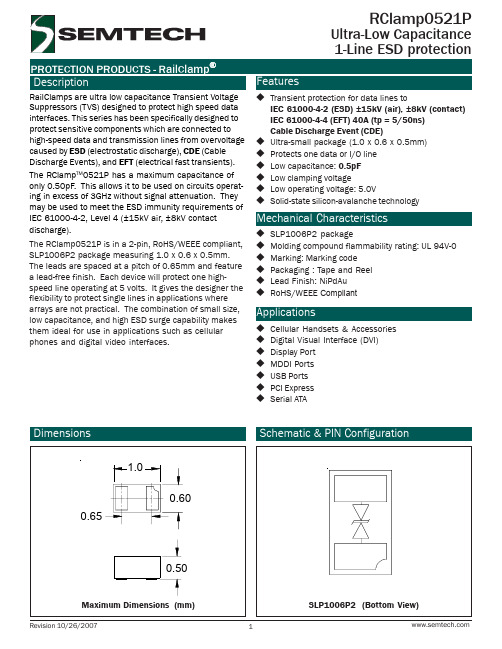
Typical 9.3
Maximum 5 11
Units V V
0.025
1
µA
15
V
25
V
0.30
0.50
pF
2007 Semtech Corp.
2
元器件交易网
RClamp0521P
Clamping Voltage - VC (V)
PROTECTION PRODUCTS Typical Characteristics
Mechanical Characteristics
SLP1006P2 package Molding compound flammability rating: UL 94V-0 Marking: Marking code Packaging : Tape and Reel Lead Finish: NiPdAu RoHS/WEEE Compliant
90 80 70 60 50 40 30 20 10
0 0
Power Derating Curve
25
50
75
100
125
150
Ambient Temperature - TA (oC)
Clamping Voltage vs. Peak Pulse Current
24 22 20 18 16 14 12 10
10 MHz
100 MHz
13 GHz GHz
START. 030 MHz
STOP 3000.000000 MHz
3
元器件交易网
PROTECTION PRODUCTS Applications Information
SONiX SN8P2501B 用户说明书
SONiX 公司保留对以下所有产品在可靠性,功能和设计方面的改进作进一步说明的权利。
SONiX 不承担由本手册所涉及的产品或电路的运用和使用所引起的任何责任,SONiX 的产品不是专门设计来应用于外科植入、生命维持和任何SONiX 产品的故障会对个体造成伤害甚至死亡的领域。
如果将SONiX 的产品应用于上述领域,即使这些是由SONiX 在产品设计和制造上的疏忽引起的,用户应赔偿所有费用、损失、合理的人身伤害或死亡所直接或间接产生的律师费用,并且用户保证SONiX 及其雇员、子公司、分支机构和销售商与上述事宜无关。
修正记录版本日期内容VER 1.0 2006年12月 1. 初版。
目 录修正记录 (2)目录 (3)11产品概述 (5)1.1 特性 (5)1.2 系统结构框图 (6)1.3 引脚配置 (7)1.4 引脚功能说明 (8)1.5 引脚电路框图 (9)22中央处理器 (CPU) (10)2.1 存储器 (10)2.1.1 程序存储器 (ROM) (10)2.1.1.1 复位向量(0000H) (11)2.1.1.2 中断向量(0008H) (12)2.1.1.3 查表 (13)2.1.1.4 跳转表 (15)2.1.1.5 CHECKSUM计算 (17)2.1.2 编译选项列表 (18)2.1.3 数据存储器(RAM) (19)2.1.4 系统寄存器 (20)2.1.4.1 系统寄存器表 (20)2.1.4.2 系统寄存器说明 (20)2.1.4.3 系统寄存器位定义 (21)2.1.4.4 累加器 (22)2.1.4.5 程序状态寄存器PFLAG (23)2.1.4.6 程序计数器 (24)Z寄存器 (26)2.1.4.7 Y,2.1.4.8 R寄存器 (26)2.2 寻址模式 (27)2.2.1 立即寻址 (27)2.2.2 直接寻址 (27)2.2.3 间接寻址 (27)2.3 堆栈 (28)2.3.1 概述 (28)2.3.2 堆栈寄存器 (29)2.3.3 堆栈操作举例 (30)33复位 (31)3.1 概述 (31)3.2 上电复位 (32)3.3 看门狗复位 (32)3.4 掉电复位 (33)3.4.1 概述 (33)3.4.2 系统工作电压 (33)3.4.3 掉电复位性能改进 (34)3.5 外部复位 (36)3.6 外部复位电路 (37)3.6.1 RC复位电路 (37)3.6.2 二极管&RC复位电路 (37)3.6.3 齐纳二极管复位电路 (38)3.6.4 电压偏置复位电路 (38)3.6.5 外部IC复位 (39)44系统时钟 (40)4.1 概述 (40)4.2 时钟框图 (40)4.3 OSCM寄存器 (41)4.4 系统高速时钟 (42)4.4.1 内部高速RC振荡器 (42)4.4.2 外部高速时钟 (43)4.4.2.1 石英/陶瓷振荡器 (43)4.4.2.2 RC振荡器 (44)4.4.2.3 外部时钟源 (44)4.5 系统低速时钟 (45)4.5.1 系统时钟测试 (45)55系统工作模式 (46)5.1 概述 (46)5.2 模式切换举例 (47)5.3 唤醒时间 (48)5.3.1 概述 (48)5.3.2 唤醒时间 (48)5.3.3 P1W唤醒控制寄存器 (48)66中断 (49)6.1 概述 (49)6.2 中断请求使能寄存器INTEN (49)6.3 中断请求寄存器INTRQ (50)6.4 GIE全局中断 (50)6.5 PUSH,POP处理 (51)6.6 INT0(P0.0)中断 (52)6.7 T0中断 (53)6.8 TC0中断 (54)6.9 多中断操作举例 (55)77定时器 (56)7.1 看门狗定时器 (56)7.2 定时器T0 (57)7.2.1 概述 (57)7.2.2 模式寄存器T0M (58)7.2.3 计数寄存器T0C (59)7.2.4 T0操作时序 (60)7.3 定时/计数器TC0 (61)7.3.1 概述 (61)7.3.2 模式寄存器TC0M (62)7.3.3 计数寄存器TC0C (63)7.3.4 自动重载寄存器TC0R (64)7.3.5 TC0时钟频率输出(蜂鸣器输出) (65)7.3.6 TC0操作举例 (66)7.4 PWM0 (67)7.4.1 概述 (67)7.4.2 TC0IRQ和PWM输出占空比 (68)7.4.3 PWM输出占空比与TC0R的变化 (69)7.4.4 PWM编程举例 (70)88 I/O端口 (71)8.1 I/O端口模式 (71)8.2 I/O口上拉电阻 (72)8.3 I/O漏极开路寄存器 (73)8.4 I/O口数据寄存器 (74)99指令表 (75)1100电气特性 (75)1111 OTP烧录引脚 (77)11.1 转接板插座对应的引脚分布图 (77)11.2 烧录引脚分布图 (78)1122 SN8P2501A升级为SN8P2501B注意事项 (79)1133封装信息 (81)13.1 P-DIP14PIN (81)13.2 SOP14PIN (82)13.3 SSOP16PIN (83)产品概述1.1 特性♦ 存储器 ♦三个中断源 OTP ROM :1K * 16 bits 两个内部中断源:T0, TC0 RAM :48 * 8 bits 一个外部中断源:INT0 四层堆栈缓存器 ♦两个8-bit 定时/计数器♦ I/O 端口 T0:0.5sec RTC 基本定时器 输入输出端口:P0, P1, P2, P5 TC0:自动重新加载定时器/计数器/蜂鸣器输出 输入端:P1.1 可编程漏极开路:P1.0 ♦内置看门狗定时器和内部时钟源 唤醒功能:P0, P1电平变缓触发 低速RC (16KHz @3V, 32KHz @5V). 带上拉电阻:P0, P1, P2, P5外部中断信号触发沿:寄存器PEDGE 控制的P0.0♦双时钟系统 外部高速时钟:RC 模式高达10MHz 外部高速时钟:晶振模式高达16MHz♦ 3-Level LVD内部高速时钟:16MHz RC 复位及电源监控系统 内部低速时钟:16KHz(3V), 32KHz(5V) RC♦ 强大的指令系统♦工作模式 单时钟指令周期 (1T) 普通模式:高、低速时钟同时工作 大部分指令仅需一个周期 低速模式:低速时钟有效 JMP 指令可以在整个ROM 区执行 睡眠模式:高、低速时钟都停止工作 CALL 指令可寻址全部ROM 区 绿色模式:由T0周期性的唤醒 查表功能 (MOVC)可用于全部ROM 区 ♦封装 PDIP 14 pins SOP 14 pins SSOP 16 pins) 特性选择列表定时器 芯片 ROM (word) RAM (Byte) 堆栈 T0 TC0 LVD层数 IHRC I/O 绿色模式低速模式PWM 蜂鸣器唤醒功能的 引脚个数封装SN8P2501A 1K 48 4 V V 1 V 12V V V 5 DIP14/SOP14/SSOP16SN8P2501B 1K 48 4 V V 3 V 12V V V 5 DIP14/SOP14/SSOP161.2 系统结构框图1.3 引脚配置SN8P2501BP (P-DIP 14 pins)SN8P2501BS (SOP 14 pins)SN8P2501BX (SSOP 16 pins)P2.2 1 U 14P2.3P2.1 2 13P2.4P2.0 3 12P2.5VDD 4 11VSSP1.3/XIN 5 10P0.0/INT0P1.2/XOUT 6 9 P1.0P1.1/RST/VPP7 8 P5.4/BZ0/PWM0SN8P2501BPSN8P2501BSP2.2 1 U 16P2.3P2.1 2 15P2.4P2.0 3 14P2.5VDD 4 13VSSVDD 5 12VSSP1.3/XIN 6 11P0.0/INT0P1.2/XOUT7 10P1.0P1.1/RST/VPP8 9 P5.4/BZ0/PWM0SN8P2501BX1.4 引脚功能说明引脚 类型 说明VDD, VSSP数字电路电源输入端P1.1/RST/VPP I, P P1.1:禁止外部复位的情况下仅作输入引脚 (施密特触发器) P1.1无内置上拉电阻;具有唤醒功能;RST :系统复位输入引脚,施密特触发器结构,低电平触发,一般处于高电平状态 VPP :OTP 烧录引脚P1.3/XIN I/OP1.3输入/输出引脚,输入时为施密特触发器结构; 内置上拉电阻;具有唤醒功能;XIN :外部振荡器(晶振或RC )有效时作为振荡器输入引脚 P1.2/XOUT I/OP1.2输入/输出引脚,输入引脚为施密特触发器结构 内置上拉电阻;唤醒功能;XOUT :外部晶振模式时作为振荡器输出引脚P0.0/INT0 I/O P0.0输入/输出引脚,输入引脚为施密特触发器结构; 内置上拉电阻;具有唤醒功能;INT0 触发引脚(施密特触发器); TC0 事件计数器时钟输入引脚;P1.0 I/OPP1.0输入/输出引脚,漏极开路输入引脚为施密特触发器结构;内置上拉电阻;P2 [5:0] I/O输入/输出引脚,输入引脚为施密特触发器结构;内置上拉电阻;P5.4/BZ0.PWM0 I/O P5.4输入/输出引脚,输入引脚为施密特触发器结构;内置上拉电阻;TC0 2分频输出引脚,PWM 和蜂鸣器引脚;1.5 引脚电路框图Port 0, 2, 5Port 1.0Port 1.2, 1.3Port 1.1Ext. Reset中央处理器 (CPU)2.1 存储器2.1.1 程序存储器 (ROM)) 1 words ROMROM0000H 复位向量用户复位向量跳至用户程序初始端0001H.. 0007H 通用区域0008H 中断向量 用户中断向量 0009H 用户程序. . 000FH 0010H 0011H. . . . . 03FCH 通用区域用户程序结束03FDH03FEH03FFH 系统保留2.1.1.1 复位向量(0000H)一个字长的系统复位向量。
product brief-CNILG 产品介绍册子资料

Isomax S 系列塑壳断路器Isomax S 系列塑壳断路器的不断发展使其成为今天市场上最大的、最完善的低压塑壳断路器家族,能够满足从小用户到工业变、配电站安装的需要。
Isomax S 系列塑壳断路器载任何条件下多具备高质量、高可靠性和高性能的特性,而且安装简便、使用安全。
持续不断的发展使 Isomax S 系列产品不断扩展,并进一步完善。
Isomax S 系列的完整性还体现在其使用上的合理化:外形尺寸、安装方式以及同断路器安装方式无关的相同的附件。
Isomax S 系列塑壳断路器的另一个重点是微处理电子脱扣器(用于160A及以上的断路器):PR211/P、PR212/P,它们都是专为电动机起动与保护而设计的。
Isomax S series circuit breakersIsomax S evolves continually and is the largest and most complete family of low voltage moulded-case circuit-breakers on the market today, able to fulfill all installation requirements, from the small user up to large industrial electrical power distribution plants.Isomax S is characterized by high quality, reliability, and performance under all conditions, simplicity of installation and safety of operation. The continual and constant evolution of the series has led to further extending the range of products, thereby making the Isomax S offer increasingly complete over time.The completeness of the series can also be noted in better rationalization of use: the overall dimensions, methods of installation and possibility of applying accessories are all the same, regardless of the type of range the circuit-breaker is placed in.Great importance is also put on the microprocessor-based electronic releases (mounted on the circuit breakers starting from 160A): PR211/P, PR212/P, and PR212/MP (specifically designed to actuate dedicated functions for motor starting and protection).自动转换开关电器自动转换开关电器(ATSE)是一种由微处理器控制,用于电网系统中网电与网电或网电与发电机电源自动切换的装置,适用于需要保持电源连续供电的场合。
Pluronic F-127说明书
碧云天生物技术/Beyotime Biotechnology 订货热线:400-168-3301或800-8283301 订货e-mail :******************技术咨询:*****************网址:碧云天网站 微信公众号Pluronic F-127产品编号 产品名称包装 ST501-0.1g Pluronic F-127 (无菌) 10%×1ml ST501-1g Pluronic F-127 1g ST501-10g Pluronic F-127 10g ST501-100gPluronic F-127100g产品简介:Pluronic F-127,也被称为Poloxamer 407,即Polyethylene-polypropylene glycol ,是一种聚氧乙烯聚氧丙烯醚三嵌段共聚物,中文名为泊洛沙姆、聚醚或聚氧乙烯聚氧丙烯,分子式为H(C 2H 4O)x (C 3H 6O)y (C 2H 4O)z OH ,分子量约为12.6kD ,熔点约56ºC ,CAS Number 9003-11-6。
本产品为细胞培养级别,进口分装。
Pluronic 是BASF 所持有的商标。
Pluronic F-127是一种新型的高分子非离子型表面活性剂,常用于增强染料的水溶性,提高脂溶性染料的细胞通透性。
此外,Pluronic F-127也常用于分离膜蛋白、处理材料表面以改变其特性,例如降低材料表面的蛋白或细胞的非特异性吸附等。
本产品的固体包装为白色粉末,可溶于水或DMSO 。
液体包装为经过滤除菌的10%(w/v)的水溶液,可以直接用于细胞实验。
Pluronic F-127可以配制成10%的水溶液,也可以配制成20%的DMSO 溶液。
溶解过程需要在40-50ºC 加热约30分钟,溶解后宜室温保存,不宜冷藏或冷冻。
如果发现有结晶析出,可以在37-50ºC 加热溶解。
零部件厂家专用PL说明资料090112

所谓的北美PL?为了降低在美国的法律风险20088年11月27日日期:200地点:WHM作成::WHM作成在这种情况下,可以要求生产者赔偿所造成的损失。
例1破裂例2缺陷产品结果例3因产品存在缺陷造成人身、、财产损害的财产损害的,,生产者或者销售者应当承担的因产品存在缺陷造成人身赔偿责任。
赔偿责任所谓的零部件生产厂家的PL责任购进零部件生产厂家购进零部件生产厂家制造的制造的制造的零部件零部件零部件,,将其组装到将其组装到GFMM GFMM GFMM中中,在北美销售在北美销售。
若由于零部件存在缺陷而使由于零部件存在缺陷而使GFMM GFMM GFMM在在北美发生事故发生事故,,造成他人身体造成他人身体、、财产的损害时害时,,零部件厂家必须对其损害承担是否要承担赔偿责任是否要承担赔偿责任??零部件生产厂家生产的零部件零部件生产厂家生产的零部件存存所谓所谓的零部件生产厂家的的零部件生产厂家的的零部件生产厂家的PLPLPL责任责任缺陷的种类设计上的制造上的警告警告缺陷缺陷(标签标签、、责任归属方如果有零部件厂家设计的样式事实事实::改变了物的规格改变了物的规格。
不能证明此点陪审员的意见陪审员的意见::回避了生产厂家的解释回避了生产厂家的解释,,认定图纸与实际物品不一致制造上的缺陷为什么图纸不能与实际物品不一致为什么图纸不能与实际物品不一致??⇒案例案例22没有得到没有得到WHM WHM WHM的承认的承认的承认,,即对规格进行更改时即对规格进行更改时。
案例1违反公司内部标准1.图纸与实际物品不一致(包括忘了粘贴时包括忘了粘贴时))FMVSS :Federal Motor Vehicle Safety Standards 的简称2.不符合不符合零部件生产厂家及零部件生产厂家及WHM 的品质标准(检查基准书检查基准书、、作业标准表作业标准表、、工程品质管理表工程品质管理表、、等)例)在抽样检在抽样检查查中,尽管规定尽管规定N=5N=5N=5,,在现实中只检查在现实中只检查n=2n=2违反公司内部标准谁判断谁判断零部件生产厂家零部件生产厂家零部件生产厂家的的「缺陷的有无缺陷的有无」」?开示制度开示制度::诉讼流程问证人起诉书问信求提出资料求对事实承或否定言取录书程序结束出陪审员庭陈述发生终辩论决2-3年约2周~1个月意味着要将意味着要将零部件生产厂家零部件生产厂家零部件生产厂家日常作成的日常作成的社内文件以及保管着的文件带出公司1.零部件生产厂家必须将保管文件零部件生产厂家必须将保管文件的复印件的复印件的复印件提出提出提出。
2501芯片
2501芯片2501芯片是一种高性能、低功耗的微控制器芯片,适用于各种嵌入式系统和物联网应用。
它基于 ARM 架构,采用先进的制程技术,提供出色的计算和通信性能。
首先,2501芯片具有强大的计算能力。
它采用了多核心设计,在低功耗的条件下实现了高频率的运行。
每个核心都配备了强大的浮点运算单元,能够加速复杂的算法和处理大量的数据。
因此,2501芯片不仅适用于一般的控制任务,还可以处理更加复杂的计算任务,例如图像处理和人工智能算法。
其次,2501芯片具有低功耗的特点。
它采用了先进的制程技术和节能的架构设计,有效降低了功耗。
即使在高负载的情况下,2501芯片也能够保持低功耗运行。
这使得它非常适合用于电池供电的设备,例如智能手表、智能家居和可穿戴设备。
同时,低功耗设计也能有效延长设备的续航时间,提升用户体验。
除了计算性能和功耗方面的优势,2501芯片还具有出色的通信功能。
它内置了多种通信接口,包括以太网、蓝牙、Wi-Fi 等。
这些通信接口可以实现与外部设备的快速数据交换,同时也可以实现与云端的连接。
这使得2501芯片可以轻松地与其他设备或者云平台进行通信,实现物联网的互联互通。
最后,2501芯片还具有丰富的外设接口和扩展能力。
它提供了多个通用输入输出引脚,可以连接各种传感器、执行器和外设。
此外,2501芯片还支持外部存储器的扩展,可以方便地存储和管理大量的数据。
这使得它适用于各种嵌入式系统的设计需求,无论是传感器数据采集、设备控制还是实时数据处理,都能够满足各种外设需求。
总的来说,2501芯片是一种高性能、低功耗的微控制器芯片,适用于各种嵌入式系统和物联网应用。
它具有强大的计算能力、低功耗、出色的通信功能和丰富的外设接口,可以满足各种复杂的计算和通信需求。
它的出现将推动物联网技术的发展,为嵌入式系统的设计和开发提供更多可能性和灵活性。
- 1、下载文档前请自行甄别文档内容的完整性,平台不提供额外的编辑、内容补充、找答案等附加服务。
- 2、"仅部分预览"的文档,不可在线预览部分如存在完整性等问题,可反馈申请退款(可完整预览的文档不适用该条件!)。
- 3、如文档侵犯您的权益,请联系客服反馈,我们会尽快为您处理(人工客服工作时间:9:00-18:30)。
Prolific Technology Inc.
7F, #48, Sec.3, Nan-Kang Rd., Taipei, Taiwan 115, ROC Tel: 886-2-2654-6363 Fax: 886-2-2654-6161 E-mail : sales@
Power Mgt.
LED
Power on Reset Regulator 3.3/2.5V
Program ROM
Turbo 8032 MCU
Program RAM Data RAM
Program ROM
EEPROM
FEATURES
Full compliance with the USB Specification v2.0 On-chip USB2.0 Phy Support both Peer to Peer and Network functions Transfer data and share resources between two or more PCs with speed up to 480Mbps. Remote NDIS specification compliant (For network function only) Embedded Turbo 8032 micro-controller Supports USB Full/High Speed Control/Interrupt/Bulk Endpoints Transfer On-Chip 3.3V-2.5V regulator for internal circuit Dual data buffer supporting two-way data transfer Supports Suspend, Resume and Remote wake-up power management features Supports external serial EEPROM to customize vender/product related information Supports LED indicator for connection and transfer status Support external customized program ROM via 100-pin LQFP package Bus powered from either USB port No glue logic needed – can be embedded in small spaces 64/100 Pins LQFP packages
BLOCK DIAGRAM
USB2.0PHY (UTMI) Bulk FIFOs USB2.0PHY (UTMI) D+/DBackend SIE
USB Host A
D+/DBackend SIE
USB Host I/F Logic Device Logic Device
元器件交易网
PL-2501 Product Brochure V1.0 09/11/02
1
PL-2501 Hi-Speed USB Host to Host Bridge Controller
OVERVIEW
The PL-2501 is a single chip Hi-Speed USB Host-to-Host Bridge Controller. With PL-2501 embedded cable, users can quickly transfer large amount and large size of files directly from one PC to another. Also it’s useful for computer data backup/restore, synchronization or file sharing. Additionally, the chip enables two or more Hi-Speed USB or USB1.1 equipped PCs to connect to each other using USB ports as a network. Since Hi-Speed USB extends the speed up to 480 Mbps – 40 times more than previous USB, the network constructed by PL-2501 has data rates almost 5 times faster than a conventional 100BT Ethernet network. Implemented with remote NDIS, users can easily build up this network at a turbo speed without the troubled installation of drivers and add-on network interface cards.
