PD-1310中文资料
UL1310 讲义
概述
UL 1310适用于由相电压不超过150V的交流电网供电的,能量级别不高 于Class 2的电源或充电器。在任何负载下,其输入功率不超过660W。
Class 2 - 代表输出有限的电压、功率、电流。
CLASS 2 – A source having limited voltage and energy capacity. Requirements for voltage and energy capacity limitations are as indicated in this standard.. The maximum output voltage under any load condition (including no load) between any two output terminations of a unit shall not be more than the peak voltages 42.4 V peak for sinusoidal or nonsinusoidal AC; 60 V for continuous DC (如果加标和美标同时做,空载不能超过 42.4VDC)
非正常测试
2. Transformer burnout 先正常工作至稳态,然后接一个能产生三倍正常输入电流或最大输出电 流的负载。试验进行至热稳态,或不可恢复的热保护器断开。自恢复的 工作7小时,手动恢复的做50个周期。
4. 负载: a)交流输出 – 可调电阻。 b)直流输出 – 可调电阻和10000uF电容并联。 c)充电器也可使用经标准放电后的电池。
泄漏电流
在 不同裸露表面,包括输出端之间,以及裸露表面(可多个同时)和接 地电源导体间测量。
ADuM1310ARWZ1资料
Triple-Channel Digital IsolatorsADuM1310/ADuM1311 Rev. Fnformation furnished by Analog Devices is believed to be accurate and reliable. However, noresponsibility is assumed by Analog Devices for its use, nor for any infringements of patents or other rights of third parties that may result from its use. Specifications subject to change without notice. No license is granted by implication or otherwise under any patent or patent rights of Analog Devices. T rademarks and registered trademarks are the property of their respective owners. One Technology Way, P.O. Box 9106, Norwood, MA 02062-9106, U.S.A. Tel: 781.329.4700 Fax: 781.461.3113 ©2004–2007 Analog Devices, Inc. All rights reserved.FEATURESLow power operation5 V operation1.7 mA per channel max @ 0 Mbps to 2 Mbps4.0 mA per channel max @ 2 Mbps to 10 Mbps3 V operation1.0 mA per channel max @ 0 Mbps to 2 Mbps2.1 mA per channel max @ 2 Mbps to 10 Mbps Bidirectional communication3 V/5 V level translationSchmitt trigger inputsHigh temperature operation: 105°CUp to 10 Mbps data rate (NRZ)Programmable default output stateHigh common-mode transient immunity: >25 kV/μs16-lead Pb-free SOIC wide body package8.1 mm external creepageSafety and regulatory approvalsUL recognition: 2500 V rms for 1 minute per UL 1577 CSA Component Acceptance Notice #5AVDE certificate of conformityDIN EN 60747-5-2 (VDE 0884 Part 2): 2003-01DIN EN 60950 (VDE 0805): 2001-12; EN 60950: 2000 V IORM = 560 V peak working voltage APPLICATIONSGeneral-purpose multichannel isolationSPI® interface/data converter isolationRS-232/RS-422/RS-485 transceiverIndustrial field bus isolationFUNCTIONAL BLOCK DIAGRAMSV DD1GND1V IAV IBV ICNCDISABLEGND1V DD2GND2V OAV OBV OCNCCTRL2GND2494-1Figure 1. ADuM1310V DD1GND1V IAV IBV OCNCCTRL1GND1V DD2GND2V OAV OBV ICNCCTRL2GND2494-2Figure 2. ADuM1311GENERAL DESCRIPTIONThe ADuM131x1 are 3-channel digital isolators based on Analog Devices, Inc. i Coupler® technology. Combining high speed CMOS and monolithic air core transformer technology, these isolation components provide outstanding performance characteristics superior to alternatives such as optocoupler devices. By avoiding the use of LEDs and photodiodes, i Coupler devices remove the design difficulties commonly associated with optocou-plers. The typical optocoupler concerns regarding uncertain current transfer ratios, maximum operating temperature, and lifetime effects are eliminated with the simple i Coupler digital interfaces and stable performance characteristics. The need for external drivers and other discrete components is eliminated with these i Coupler products. Furthermore, i Coupler devices consume one-tenth to one-sixth the power of optocouplers at comparable signal data rates. The i Coupler also offers higher channel densities and more options for channel directionality. The ADuM131x isolators provide three independent isolation channels in a variety of channel configurations and data rates up to 10 Mbps (see the Ordering Guide). All models operate with the supply voltage on either side ranging from 2.7 V to 5.5 V, providing compatibility with lower voltage systems as well as enabling voltage translation functionality across the isolation barrier. All products allow the user to predetermine the default output state in the absence of input V DD1 power with a simple control pin. Unlike other optocoupler alternatives, the ADuM131x isolators have a patented refresh feature that ensures dc correctness in the absence of input logic transitions and during power-up/ power-down conditions.1 Protected by U.S. Patents 5,952,849; 6,873,065; and 7,075 329. Other patents pending.ADuM1310/ADuM1311Rev. F | Page 2 of 20TABLE OF CONTENTSFeatures..............................................................................................1 Applications.......................................................................................1 Functional Block Diagrams.............................................................1 General Description.........................................................................1 Revision History...............................................................................2 Specifications.....................................................................................3 Electrical Characteristics—5 V Operation................................3 Electrical Characteristics—3 V Operation................................5 Electrical Characteristics—Mixed 5 V/3 V or 3 V/5 VOperation.......................................................................................7 Package Characteristics.............................................................10 Regulatory Information.............................................................10 Insulation and Safety-Related Specifications..........................10 DIN EN 60747-5-2 (VDE 0884 Part 2) InsulationCharacteristics............................................................................11 Recommended Operating Conditions....................................11 Absolute Maximum Ratings.........................................................12 ESD Caution................................................................................12 Pin Configurations and Function Descriptions.........................13 Typical Performance Characteristics...........................................16 Application Information................................................................18 PC Board Layout........................................................................18 Propagation Delay Related Parameters....................................18 DC Correctness and Magnetic Field Immunity.....................18 Power Consumption..................................................................19 Outline Dimensions.......................................................................20 Ordering Guide.. (20)REVISION HISTORY1/07—Rev. E to Rev. FAdded ADuM1311.............................................................Universal Changes to Typical Performance Characteristics.......................16 Changes to Ordering Guide..........................................................20 10/06—Rev. D to Rev. ERemoved ADuM1410........................................................Universal Updated Format..................................................................Universal Change to Figure 3.........................................................................10 Changes to Table 10........................................................................10 Changes to Application Information...........................................12 Updated Outline Dimensions.......................................................18 Changes to Ordering Guide..........................................................18 3/06—Rev. C to Rev. DAdded Note 1 and Changes to Figure 2..........................................1 Changes to Absolute Maximum Ratings.....................................11 11/05—Rev. SpB to Rev. C5/05—Rev. SpA to Rev. SpBChanges to Table 6.............................................................................9 10/04—Data Sheet Changed from Rev. Sp0 to Rev. SpAChanges to Table 5.............................................................................9 6/04—Revision Sp0: Initial VersionADuM1310/ADuM1311Rev. F | Page 3 of 20SPECIFICATIONSELECTRICAL CHARACTERISTICS—5 V OPERATION 14.5 V ≤ V DD1 ≤5.5 V , 4.5 V ≤ V DD2 ≤ 5.5 V; all min/max specifications apply over the entire recommended operation range, unless otherwise noted; all typical specifications are at T A = 25°C, V DD1 = V DD2 = 5 V . Table 1.Parameter Symbol Min Typ Max Unit Test Conditions DC SPECIFICATIONSADuM1310, Total Supply Current,Three Channels 2DC to 2 Mbps V DD1 Supply Current I DD1 (Q) 2.4 3.2 mA DC to 1 MHz logic signal frequency V DD2 Supply Current I DD2 (Q) 1.2 1.6 mA DC to 1 MHz logic signal frequency 10 Mbps (BRW Grade Only) V DD1 Supply Current I DD1 (10) 6.6 9.0 mA 5 MHz logic signal frequency V DD2 Supply Current I DD2 (10) 2.1 3.0 mA 5 MHz logic signal frequencyADuM1311, Total Supply Current,Three Channels 2DC to 2 Mbps V DD1 Supply Current I DD1 (Q) 2.2 2.8 mA DC to 1 MHz logic signal frequency V DD2 Supply Current I DD2 (Q) 1.8 2.4 mA DC to 1 MHz logic signal frequency 10 Mbps (BRW Grade Only) V DD1 Supply Current I DD1 (10) 4.5 5.7 mA 5 MHz logic signal frequency V DD2 Supply Current I DD2 (10) 3.5 4.3 mA 5 MHz logic signal frequency For All Models Input Currents I IA , I IB , I IC , I CTRL1, I CTRL2, I DISABLE −10 +0.01 +10 μA 0 ≤ V IA , V IB , V IC ≤ V DD1 or V DD2,0 ≤ V CTRL1, V CTRL2 ≤ V DD1 or V DD2,0 ≤ V DISABLE ≤ V DD1Logic High Input Threshold V IH 2.0 VLogic Low Input ThresholdV IL 0.8 V V DD1, V DD2 − 0.1 5.0 V I Ox = −20 μA, V Ix = V IxH Logic High Output Voltages V OAH , V OBH ,V OCH V DD1, V DD2 − 0.4 4.8 V I Ox = −4 mA, V Ix = V IxH0.0 0.1 V I Ox = 20 μA, V Ix = V IxLLogic Low Output Voltages V OAL , V OBL , V OCL 0.2 0.4 V I Ox = 4 mA, V Ix = V IxLSWITCHING SPECIFICATIONS ADuM131xARWMinimum Pulse Width 3PW 1000 ns C L = 15 pF, CMOS signal levels Maximum Data Rate 4 1 Mbps C L = 15 pF, CMOS signal levelsPropagation Delay 5t PHL , t PLH 20 100 ns C L = 15 pF, CMOS signal levelsPulse Width Distortion, |t PLH − t PHL |5PWD 40 ns C L = 15 pF, CMOS signal levels Propagation Delay Skew 6t PSK 50 ns C L = 15 pF, CMOS signal levelsChannel-to-Channel Matching 7t PSKCD/OD 50 ns C L = 15 pF, CMOS signal levels ADuM131xBRWMinimum Pulse Width 3PW 100 ns C L = 15 pF, CMOS signal levels Maximum Data Rate 4 10 Mbps C L = 15 pF, CMOS signal levelsPropagation Delay 5t PHL , t PLH 20 30 50 ns C L = 15 pF, CMOS signal levelsPulse Width Distortion, |t PLH − t PHL |5PWD 5 ns C L = 15 pF, CMOS signal levels Change vs. Temperature 5 ps/°C C L = 15 pF, CMOS signal levelsPropagation Delay Skew 6t PSK 30 ns C L = 15 pF, CMOS signal levelsChannel-to-Channel Matching,Codirectional Channels7t PSKCD 5 ns C L = 15 pF, CMOS signal levels Channel-to-Channel Matching,Opposing-Directional Channelst PSKOD 6 ns C L = 15 pF, CMOS signal levelsADuM1310/ADuM1311Rev. F | Page 4 of 20Parameter Symbol Min Typ Max Unit Test Conditions For All Models Output Rise/Fall Time (10% to 90%) t R /t F 2.5 ns C L = 15 pF, CMOS signal levelsCommon-Mode Transient Immunity at Logic High Output8|CM H | 25 35 kV/μs V Ix = V DD1/V DD2, V CM = 1000 V,transient magnitude = 800 VCommon-Mode Transient Immunity at Logic Low Output |CM L | 25 35 kV/μs V Ix = 0 V, V CM = 1000 V,transient magnitude = 800 V Refresh Rate f r 1.2 MbpsInput Enable Time 9t ENABLE 2.0 μs V IA , V IB , V IC = 0 V or V DD1Input Disable Time 9t DISABLE 5.0 μs V IA , V IB , V IC = 0 V or V DD1Input Supply Current per Channel, Quiescent 10I DDI (Q)0.50 0.73 mA Output Supply Current perChannel, Quiescent10I DDO (Q) 0.38 0.53 mA Input Dynamic Supply Current per Channel 11I DDI (D) 0.12 mA/MbpsOutput Dynamic Supply Current per Channel 11I DDO (D) 0.04 mA/Mbps1 All voltages are relative to their respective ground.2The supply current values for all four channels are combined when running at identical data rates. Output supply current values are specified with no output load present. The supply current associated with an individual channel operating at a given data rate can be calculated as described in the Power Consumption section. See Figure 6 through Figure 8 for information on per-channel supply current as a function of data rate for unloaded and loaded conditions. See Figure 9 through Figure 12 for total V DD1 and V DD2 supply currents as a function of data rate for ADuM1310/ADuM1311 channel configurations. 3The minimum pulse width is the shortest pulse width at which the specified pulse width distortion is guaranteed. 4The maximum data rate is the fastest data rate at which the specified pulse width distortion is guaranteed. 5t PHL propagation delay is measured from the 50% level of the falling edge of the V Ix signal to the 50% level of the falling edge of the V Ox signal. t PLH propagation delay is measured from the 50% level of the rising edge of the V Ix signal to the 50% level of the rising edge of the V Ox signal. 6t PSK is the magnitude of the worst-case difference in t PHL or t PLH that is measured between units at the same operating temperature, supply voltages, and output load within the recommended operating conditions. 7Codirectional channel-to-channel matching is the absolute value of the difference in propagation delays between any two channels with inputs on the same side of the isolation barrier. Opposing-directional channel-to-channel matching is the absolute value of the difference in propagation delays between any two channels with inputs on opposing sides of the isolation barrier. 8CM H is the maximum common-mode voltage slew rate that can be sustained while maintaining V O > 0.8 V DD2. CM L is the maximum common-mode voltage slew rate that can be sustained while maintaining V O < 0.8 V. The common-mode voltage slew rates apply to both rising and falling common-mode voltage edges. The transient magnitude is the range over which the common mode is slewed. 9Input enable time is the duration from when V DISABLE is set low until the output states are guaranteed to match the input states in the absence of any input data logic transitions. If an input data logic transition within a given channel does occur within this time interval, the output of that channel reaches the correct state within the much shorter duration, as determined by the propagation delay specifications within this data sheet. Input disable time is the duration from when V DISABLE is set high until the output states are guaranteed to reach their programmed output levels, as determined by the CTRL 2 logic state (see Table 12). 10I DDx (Q) is the quiescent current drawn from the corresponding supply by a single channel. To calculate the total quiescent current, an additional inaccessible channel in the same orientation as Channel A must be included to account for the total current consumed. 11Dynamic supply current is the incremental amount of supply current required for a 1 Mbps increase in signal data rate. See Figure 6 through Figure 8 for information on per-channel supply current for unloaded and loaded conditions. See the Power Consumption section for guidance on calculating the per-channel supply current for a given data rate.ADuM1310/ADuM1311Rev. F | Page 5 of 20ELECTRICAL CHARACTERISTICS—3 V OPERATION 12.7 V ≤ V DD1 ≤3.6 V , 2.7 V ≤ V DD2 ≤ 3.6 V; all min/max specifications apply over the entire recommended operation range, unless otherwise noted; all typical specifications are at T A = 25°C, V DD1 = V DD2 = 3.0 V . Table 2.Parameter Symbol Min Typ Max Unit Test Conditions DC SPECIFICATIONSADuM1310, Total Supply Current,Three Channels 2 DC to 2 Mbps V DD1 Supply Current I DD1 (Q) 1.2 1.6 mA DC to 1 MHz logic signal frequency V DD2 Supply Current I DD2 (Q) 0.8 1.0 mA DC to 1 MHz logic signal frequency 10 Mbps (BRW Grade Only) V DD1 Supply Current I DD1 (10) 3.4 4.9 mA 5 MHz logic signal frequency V DD2 Supply Current I DD2 (10) 1.1 1.3 mA 5 MHz logic signal frequencyADuM1311, Total Supply Current,Three Channels 2DC to 2 Mbps V DD1 Supply Current I DD1 (Q) 1.0 1.6 mA DC to 1 MHz logic signal frequency V DD2 Supply Current I DD2 (Q) 0.9 1.4 DC to 1 MHz logic signal frequency 10 Mbps (BRW Grade Only) V DD1 Supply Current I DD1 (10) 2.5 3.5 mA 5 MHz logic signal frequency V DD2 Supply Current I DD2 (10) 1.9 2.6 5 MHz logic signal frequency For All Models Input Currents I IA , I IB , I IC , I CTRL1, I CTRL2, I DISABLE −10 +0.01 +10 μA 0 ≤ V IA , V IB , V IC ≤ V DD1 or V DD2,0 ≤ V CTRL1, V CTRL2 ≤ V DD1 or V DD2,0 ≤ V DISABLE ≤ V DD1Logic High Input Threshold V IH 1.6 VLogic Low Input ThresholdV IL 0.4 V V DD1, V DD2 − 0.1 3.0 V I Ox = −20 μA, V Ix = V IxHLogic High Output Voltages V OAH , V OBH , V OCH V DD1, V DD2 − 0.4 2.8 V I Ox = −4 mA, V Ix = V IxH0.0 0.1 V I Ox = 20 μA, V Ix = V IxLLogic Low Output Voltages V OAL , V OBL , V OCL 0.2 0.4 V I Ox = 4 mA, V Ix = V IxLSWITCHING SPECIFICATIONS ADuM131xARW Minimum Pulse Width 3PW 1000 ns C L = 15 pF, CMOS signal levelsMaximum Data Rate 41 Mbps C L = 15 pF, CMOS signal levels Propagation Delay 5t PHL , t PLH 20 100 ns C L = 15 pF, CMOS signal levelsPulse Width Distortion, |t PLH − t PHL |5PWD 40 ns C L = 15 pF, CMOS signal levels Propagation Delay Skew 6t PSK 50 ns C L = 15 pF, CMOS signal levelsChannel-to-Channel Matching 7t PSKCD/OD 50 ns C L = 15 pF, CMOS signal levels ADuM131xBRW Minimum Pulse Width 3PW 100 ns C L = 15 pF, CMOS signal levelsMaximum Data Rate 410 Mbps C L = 15 pF, CMOS signal levels Propagation Delay 5t PHL , t PLH 20 30 50 ns C L = 15 pF, CMOS signal levelsPulse Width Distortion, |t PLH − t PHL |5PWD 5 ns C L = 15 pF, CMOS signal levels Change vs. Temperature 5 ps/°C C L = 15 pF, CMOS signal levelsPropagation Delay Skew 6t PSK 30 ns C L = 15 pF, CMOS signal levelsChannel-to-Channel Matching,Codirectional Channels7t PSKCD 5 ns C L = 15 pF, CMOS signal levels Channel-to-Channel Matching, Opposing-Directional Channels7t PSKOD 6 ns C L = 15 pF, CMOS signal levelsADuM1310/ADuM1311Rev. F | Page 6 of 20Parameter Symbol Min Typ Max Unit Test Conditions For All Models Output Rise/Fall Time (10% to 90%) t R /t F 2.5 ns C L = 15 pF, CMOS signal levelsCommon-Mode Transient Immunity at Logic High Output 8|CM H | 25 35 kV/μs V Ix = V DD1/V DD2, V CM = 1000 V,transient magnitude = 800 VCommon-Mode Transient Immunity at Logic Low Output 8|CM L | 25 35 kV/μs V Ix = 0 V, V CM = 1000 V,transient magnitude = 800 V Refresh Rate f r 1.1 Mbps Input Enable Time 9t ENABLE 2.0 μs V IA , V IB , V IC = 0 V or V DD1Input Disable Time 9t DISABLE 5.0 μs V IA , V IB , V IC = 0 V or V DD1Input Supply Current per Channel,Quiescent10I DDI (Q) 0.25 0.38 mA Output Supply Current per Channel, Quiescent10I DDO (Q)0.19 0.33 mA Input Dynamic Supply Current per Channel 11I DDI (D) 0.07 mA/MbpsOutput Dynamic Supply Current per Channel 11I DDO (D) 0.02 mA/Mbps1 All voltages are relative to their respective ground.2The supply current values for all four channels are combined when running at identical data rates. Output supply current values are specified with no output load present. The supply current associated with an individual channel operating at a given data rate can be calculated as described in the Power Consumption section. See Figure 6 through Figure 8 for information on per-channel supply current as a function of data rate for unloaded and loaded conditions. See Figure 9 through Figure 12 for total V DD1 and V DD2 supply currents as a function of data rate for ADuM1310/ADuM1311 channel configurations. 3The minimum pulse width is the shortest pulse width at which the specified pulse width distortion is guaranteed. 4The maximum data rate is the fastest data rate at which the specified pulse width distortion is guaranteed. 5t PHL propagation delay is measured from the 50% level of the falling edge of the V Ix signal to the 50% level of the falling edge of the V Ox signal. t PLH propagation delay is measured from the 50% level of the rising edge of the V Ix signal to the 50% level of the rising edge of the V Ox signal. 6t PSK is the magnitude of the worst-case difference in t PHL or t PLH that is measured between units at the same operating temperature, supply voltages, and output load within the recommended operating conditions. 7Codirectional channel-to-channel matching is the absolute value of the difference in propagation delays between any two channels with inputs on the same side of the isolation barrier. Opposing-directional channel-to-channel matching is the absolute value of the difference in propagation delays between any two channels with inputs on opposing sides of the isolation barrier. 8CM H is the maximum common-mode voltage slew rate that can be sustained while maintaining V O > 0.8 V DD2. CM L is the maximum common-mode voltage slew rate that can be sustained while maintaining V O < 0.8 V. The common-mode voltage slew rates apply to both rising and falling common-mode voltage edges. The transient magnitude is the range over which the common mode is slewed. 9Input enable time is the duration from when V DISABLE is set low until the output states are guaranteed to match the input states in the absence of any input data logic transitions. If an input data logic transition within a given channel does occur within this time interval, the output of that channel reaches the correct state within the much shorter duration, as determined by the propagation delay specifications within this data sheet. Input disable time is the duration from when V DISABLE is set high until the output states are guaranteed to reach their programmed output levels, as determined by the CTRL 2 logic state (See Table 12). 10I DDx (Q) is the quiescent current drawn from the corresponding supply by a single channel. To calculate the total quiescent current, an additional inaccessible channel in the same orientation as Channel A must be included to account for the total current consumed. 11Dynamic supply current is the incremental amount of supply current required for a 1 Mbps increase in signal data rate. See Figure 6 through Figure 8 for information on per-channel supply current for unloaded and loaded conditions. See the Power Consumption section for guidance on calculating the per-channel supply current for a given data rate.ADuM1310/ADuM1311Rev. F | Page 7 of 20ELECTRICAL CHARACTERISTICS—MIXED 5 V/3 V OR 3 V/5 V OPERATION 15 V/3 V operation: 4.5 V ≤ V DD1 ≤ 5.5 V , 2.7 V ≤ V DD2 ≤ 3.6 V; 3 V/5 V operation: 2.7 V ≤ V DD1 ≤ 3.6 V , 4.5 V ≤ V DD2 ≤ 5.5 V; all min/max specifications apply over the entire recommended operation range, unless otherwise noted; all typical specifications are at T A = 25°C; V DD1 = 3.0 V , V DD2 = 5 V or V DD1 = 5 V , V DD2 = 3.0 V . Table 3.Parameter Symbol Min Typ Max Unit Test Conditions DC SPECIFICATIONSADuM1310, Total Supply Current,Three Channels 2DC to 2 Mbps V DD1 Supply Current I DD1 (Q) 5 V/3 V Operation 2.4 3.2 mA DC to 1 MHz logic signal frequency 3 V/5 V Operation 1.2 1.6 mA DC to 1 MHz logic signal frequency V DD2 Supply Current I DD2 (Q) 5 V/3 V Operation 0.8 1.0 mA DC to 1 MHz logic signal frequency 3 V/5 V Operation 1.2 1.6 mA DC to 1 MHz logic signal frequency 10 Mbps (BRW Grade Only) V DD1 Supply Current I DD1 (10) 5 V/3 V Operation 6.5 8.2 mA 5 MHz logic signal frequency 3 V/5 V Operation 3.4 4.9 mA 5 MHz logic signal frequency V DD2 Supply Current I DD2 (10) 5 V/3 V Operation 1.1 1.3 mA 5 MHz logic signal frequency 3 V/5 V Operation 1.9 2.2 mA 5 MHz logic signal frequencyADuM1311, Total Supply Current,Three Channels 2DC to 2 Mbps V DD1 Supply Current I DD1 (Q) 5 V/3 V Operation 2.2 2.8 mA DC to 1 MHz logic signal frequency 3 V/5 V Operation 1.0 1.6 mA DC to 1 MHz logic signal frequency V DD2 Supply Current I DD2 (Q) 5 V/3 V Operation 0.9 1.4 mA DC to 1 MHz logic signal frequency 3 V/5 V Operation 1.8 2.4 mA DC to 1 MHz logic signal frequency 10 Mbps (BRW Grade Only) V DD1 Supply Current I DD1 (10) 5 V/3 V Operation 4.5 5.7 mA 5 MHz logic signal frequency 3 V/5 V Operation 2.5 3.5 mA 5 MHz logic signal frequency V DD2 Supply Current I DD2 (10) 5 V/3 V Operation 1.9 2.6 mA 5 MHz logic signal frequency 3 V/5 V Operation 3.5 4.3 mA 5 MHz logic signal frequency For All Models Input Currents I IA , I IB , I IC , I CTRL1, I CTRL2, I DISABLE −10 +0.01 +10 μA 0 ≤ V IA , V IB , V IC ≤ V DD1 or V DD2,0 ≤ V CTRL1, V CTRL2 ≤ V DD1 or V DD2,0 ≤ V DISABLE ≤ V DD1Logic High Input ThresholdV IH V DDx = 5 V Operation 2.0 V V DDx = 3 V Operation 1.6 VLogic Low Input ThresholdV IL V DDx = 5 V Operation 0.8 V V DDx = 3 V Operation 0.4 V V DD1, V DD2 − 0.1V DD1, V DD2 V I Ox = −20 μA, V Ix = V IxHLogic High Output Voltages V OAH , V OBH , V OCH V DD1, V DD2 − 0.4V DD1, V DD2 − 0.2 V I Ox = −4 mA, V Ix = V IxH0.0 0.1 V I Ox = 20 μA, V Ix = V IxLLogic Low Output Voltages V OAL, V OBL, V OCL 0.2 0.4 V I Ox = 4 mA, V Ix = V IxLADuM1310/ADuM1311Rev. F | Page 8 of 20Parameter Symbol Min Typ Max Unit Test Conditions SWITCHING SPECIFICATIONS ADuM131xARWMinimum Pulse Width 3PW 1000 ns C L = 15 pF, CMOS signal levels Maximum Data Rate 4 1 Mbps C L = 15 pF, CMOS signal levelsPropagation Delay 5t PHL , t PLH 25 100 ns C L = 15 pF, CMOS signal levels Pulse Width Distortion, |t PLH − t PHL |5PWD 40 ns C L = 15 pF, CMOS signal levelsPropagation Delay Skew 6t PSK 50 ns C L = 15 pF, CMOS signal levelsChannel-to-Channel Matching 7t PSKCD/OD 50 ns C L = 15 pF, CMOS signal levels ADuM131xBRWMinimum Pulse Width 3PW 100 ns C L = 15 pF, CMOS signal levels Maximum Data Rate 4 10 Mbps C L = 15 pF, CMOS signal levelsPropagation Delay 5t PHL , t PLH 20 60 ns C L = 15 pF, CMOS signal levels Pulse Width Distortion, |t PLH − t PHL |5PWD 5 ns C L = 15 pF, CMOS signal levels Change vs. Temperature 5 ps/°C C L = 15 pF, CMOS signal levelsPropagation Delay Skew 6t PSK 30 ns C L = 15 pF, CMOS signal levelsChannel-to-Channel Matching,Codirectional Channels7t PSKCD 5 ns C L = 15 pF, CMOS signal levels Channel-to-Channel Matching, Opposing-Directional Channels 7t PSKOD 6 ns C L = 15 pF, CMOS signal levels For All Models Output Rise/Fall Time (10% to 90%) t R /t F C L = 15 pF, CMOS signal levels 5 V/3 V Operation 2.5 ns 3 V/5 V Operation 2.5 nsCommon-Mode Transient Immunity at Logic High Output 8|CM H | 25 35 kV/μs V Ix = V DD1/V DD2, V CM = 1000 V,transient magnitude = 800 VCommon-Mode Transient Immunity at Logic Low Output 8|CM L | 25 35 kV/μs V Ix = 0 V, V CM = 1000 V,transient magnitude = 800 V Refresh Rate f r 5 V/3 V Operation 1.2 Mbps 3 V/5 V Operation 1.1 MbpsInput Enable Time 9t ENABLE 2.0 μs V IA , V IB , V IC , V ID = 0 V or V DD1Input Disable Time 9t DISABLE 5.0 μs V IA , V IB , V IC , V ID = 0 V or V DD1Input Supply Current per Channel, Quiescent10V DDx = 5 V Operation I DDI (Q) 0.50 0.73 mA V DDx = 3 V Operation I DDI (Q) 0.25 0.38 mAOutput Supply Current per Channel, Quiescent10V DDx = 5 V Operation I DDO (Q) 0.38 0.53 mA V DDx = 3 V Operation I DDO (Q) 0.19 0.33 mAInput Dynamic Supply Currentper Channel11I DDI (D) V DDx = 5 V Operation 0.12 mA/MbpsV DDx = 3 V Operation 0.07 mA/MbpsADuM1310/ADuM1311Rev. F | Page 9 of 20Parameter Symbol Min Typ Max Unit Test ConditionsOutput Dynamic Supply Currentper ChannelI DDI (D) V DDx = 5 V Operation 0.04 mA/MbpsV DDx = 3 V Operation 0.02 mA/Mbps1 All voltages are relative to their respective ground.2The supply current values for all four channels are combined when running at identical data rates. Output supply current values are specified with no output load present. The supply current associated with an individual channel operating at a given data rate can be calculated as described in the Power Consumption section. See Figure 6 through Figure 8 for information on per-channel supply current as a function of data rate for unloaded and loaded conditions. See Figure 9 through Figure 12 for total V DD1 and V DD2 supply currents as a function of data rate for ADuM1310/ADuM1311 channel configurations. 3The minimum pulse width is the shortest pulse width at which the specified pulse width distortion is guaranteed. 4The maximum data rate is the fastest data rate at which the specified pulse width distortion is guaranteed. 5t PHL propagation delay is measured from the 50% level of the falling edge of the V Ix signal to the 50% level of the falling edge of the V Ox signal. t PLH propagation delay is measured from the 50% level of the rising edge of the V Ix signal to the 50% level of the rising edge of the V Ox signal. 6t PSK is the magnitude of the worst-case difference in t PHL or t PLH that is measured between units at the same operating temperature, supply voltages, and output load within the recommended operating conditions. 7Codirectional channel-to-channel matching is the absolute value of the difference in propagation delays between any two channels with inputs on the same side of the isolation barrier. Opposing-directional channel-to-channel matching is the absolute value of the difference in propagation delays between any two channels with inputs on opposing sides of the isolation barrier. 8CM H is the maximum common-mode voltage slew rate that can be sustained while maintaining V O > 0.8 V DD2. CM L is the maximum common-mode voltage slew rate that can be sustained while maintaining V O < 0.8 V. The common-mode voltage slew rates apply to both rising and falling common-mode voltage edges. The transient magnitude is the range over which the common mode is slewed. 9Input enable time is the duration from when V DISABLE is set low until the output states are guaranteed to match the input states in the absence of any input data logic transitions. If an input data logic transition within a given channel does occur within this time interval, the output of that channel reaches the correct state within the much shorter duration, as determined by the propagation delay specifications within this data sheet. Input disable time is the duration from when V DISABLE is set high until the output states are guaranteed to reach their programmed output levels, as determined by the CTRL 2 logic state (See Table 12). 10I DDx (Q) is the quiescent current drawn from the corresponding supply by a single channel. To calculate the total quiescent current, an additional inaccessible channel in the same orientation as Channel A must be included to account for the total current consumed. 11Dynamic supply current is the incremental amount of supply current required for a 1 Mbps increase in signal data rate. See Figure 6 through Figure 8 for information on per-channel supply current for unloaded and loaded conditions. See the Power Consumption section for guidance on calculating the per-channel supply current for a given data rate.。
1310nm1550nmDFB激光器
1310nm/1550nmDFB激光器
1310nm/1550nm尾纤型DFB激光器,采用同轴封装并耦合尾纤的方式进行输出,输出功率可达2.5mW。
具有低工作
电流,高效率,高稳定性的特点。
与我公司提供的配套驱动电路一起使用,可以获得高稳定性激光光源 。
图片仅
供参考,尺寸以实物为准,我公司(深圳市飞博源光电)热忱为您提供,具体性能指标见每支设备参数.特 点
·低工作电流·高稳定性
·高效率·同轴封装
·内置监视器
性能指标
典型最大单位波长(1310)130713101313nm 波长(1550)1547 15501553 nm 阈值电流10mA 工作电流30mA 工作电压 1.5V 出纤光功率 2.5mW 背光监控电流0.050.3mA 工作频率DC 2.5GHZ 边模抑制比30dB 工作温度-20-70℃储藏温度-40-85℃。
ADuM1310中文

七、管脚封装图
※ 品选型表
通道 分布 3/0 3/0 2/1 2/1 传输速率 (Mbps) 1 10 1 10 最大传输 延时(ns) 100 50 100 50 最大脉宽 失真(ns) 40 5 40 5 工作温度范 围(℃) -40~105 -40~105 -40~105 -40~105
二、产品特性
� � � � � � � 三通道隔离 电平转换器 传输速率:1M/10Mbps 传输延迟:50ns 瞬态共模抑制能力:25KV/us 隔离电压:2500V 工作温度:-40℃~105℃ 工作电压:3V/5V
� �
SOIC-16 宽体无铅封装
低功耗
7 mA / 通道 @ 0 Mbps 5 V operation 1. 1.7 to 2 Mbps 4.0 mA /通道 @ 10 Mbps 3 V operation 1.0 mA /通道 @ 0 Mbps to 2 Mbps mA/ 2.1 mA /通道@ 10 Mbps
ADuM1 31x ADuM13
5、 直流校正功能
磁隔离器每一通道的两组线圈起到脉冲变压器的作用, 输入端逻辑电平的变化会引起一 个窄脉冲(1ns) ,经过脉冲变压器耦合到解码器,然后再经过一个施密特触发器的波形变换 输出标准的矩形波, 如果输入端逻辑电平超过 1µs 都没有任何变化, 则校正电路会产生一个 适当极性的校正脉冲,以确保变压器直流端输出信号的正确性,如果解码器一端超过 5µs 都没有收到任何校正脉冲,则会认为输入端已经掉电或不工作,由看门狗电定时器电路,将 输出端强行置为默认状态(参看真值表) 。这确保了磁耦可以传输直流信号。
ADuM1 31x ADuM13
当 VDD1=VDD2=3V,TA=25℃ 工作参数 工作电压 符号 VDD1 VDD2 静态工作电流 IDDI(Q) IDDO(Q) 0~2Mbps 时 1310 工作电流 0~2Mbps 时 1311 工作电流 输入电平 IDD1 IDD2 IDD1 IDD2 VIH VIL 输出电平 VOH VOL 最大输出电流 IO1(side1) IO2(side2) -18 -22 VDD1,2-0.1 3.0 0.0 0.1 18 22 1.6 0.4 Min 2.7 2.7 Typ 3.0 3.0 0.25 0.19 1.2 0.8 1.0 0.9 Max 3.6 3.6 0.38 0.33 1.6 1.0 1.6 1.4 单位 V V mA mA mA mA mA mA V V V V mA mA
24V1.5A1310电源规格书讲解
CUSTOMER
客户
CUSTOMERPART
NO客户型号
MANUFACTURER
承制方
FAGE
页码
2OF6
EDITION
版本
A
1、描述(SCOPE):
格书适应于24V1.5 A型号的适配器。
The document is to specify the functional requirements of a 36W switching power supply.
客户确认签章
APPROVED SIGNATURE
DATE:
DATE:
DATE:
客户确认签字,盖章后请返回承认书一份
PLEASE RETURN TO US ONE COPY OF“SPECIFICATION FOR
APPROVAL”WITH YOUR APPROVED SIGNATURE
深圳市易创峰电源有限公司
2、输入特性(INPUT CHARACTERISTICS):
2.1输入电压(Input Voltage):
额定电压(Nominal Voltage):100-240Vac
调整范围(Variation Range):90-264Vac
2.2输入频率(Input Frequency):
额定频率(Nominal Frequency):50/60Hz
调整频率(Variation Frequency):47-63Hz
2.3输入电流(Input Current):
当输入交流电压为额定值的下限时,输出电压负载满载,最大输入交流电流1.6A。
1.6Arms max At any input vorated load.
1310nm 光发射机(PWL 4100s)
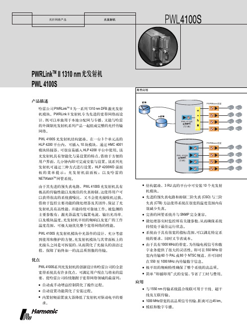
!
PWL4100S
PWRLinkTM II 1310 nm PWL 4100S
!
! PWRLink II
TM
!
!
前端
PWRBlazer݂ᅦ
光
! 1310 nm DFB
!
分前端 PWL 4112S 光发射机 (12 dB)
!PWRLink II
!"#$%&'()*+
分 路 器
!"#$%&'()*+,!" !"#$%&'()*+,-./ "012 !"#$%& !" HMC 4001 !"#
PWL 4103S 光发射机 (3 dB)
!"#$% 10
!
!"#$%& ' ()*+, !"# !"#$%&'() !"#$%&'( !"#$%&'()*+,-./0 !"#$%& !"#$%&' !" !"#$ !" PWL 4100S ! !
!"#$%&'()*"# (CSO) (CTB) !"#$%&'()*+,!"# !"#$%& SNMP !" !"# !"#$ !"#$%& 550 MHz ! !"#$%&'()*+, !"#$%&'( !"#$%&'()*+ !" !"#$% ! 1000 MHz ! !"#$%&'()* ! 60 PAL 80 NTSC 550 1000 MHz !" !"#$% !" !"#$%&
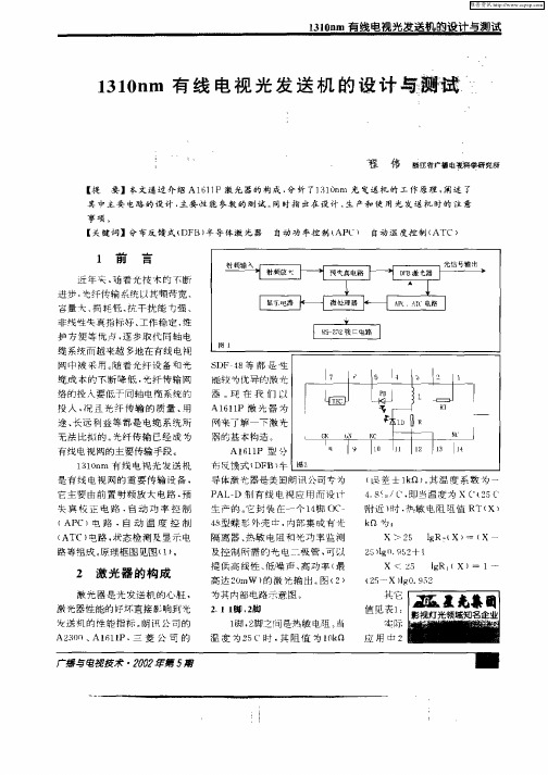
1310nm波长光发射机的原理与维护
经济 型光 发射机 占有 近 5 % 的市场 份额 , 种 光 0 这 发 射机 一个 最鲜 明的特 征就 是在 保证 整机 基本 指标 的 前 提下 , 采用 低档 的元 器 件和 简单 的控 制技 术 , 成本 相
对较 低 , 价格 也便 宜 。其 常见 结构 如 下 :
频信号经过 R 放大 、 F 电控衰减和预失真补偿后 , 直接驱 动激光器 , 得光输 出强度随着 射频信 号强度 的变化 而 使 变化 。为保 证激 光器 能稳 定 工作 ,T A C是必 需 的 , 一般
控制 也是优 良的光发射机所 必需 的。 在 直接 强度 调制 过 程 中 , 随着 射 频 信 号 强度 的 变 化, 光频 率 ( 或波 长 ) 变化 , 是 附加 的 频率 调 制 , 也 这 是 不需 要 的调频 效应 , 这些 附加 频 率 的 光 在 光纤 中传 输 时会 引起 色散 , 光传 输系 统非 线性 失真 的原 因之 一 , 是 因此 直接 调制 光发 射机 的二次失 真 产物特 别 是组合 二 阶失 真 ( s 较 多 ,/ S c o) C C O较 低 , 大约 6 B左 右 。直 Od 接调 制光 发 射 机 输 出 的 光 功 率 也 比较 小 , 多 在 2 大 O m 以下 。但 由于这种 光发 射 机结 构 简单 、 本 较 低 , W 成
中人员开支 1 0 多万元 , 0 3 公用支 出包括更新设备 、 办 公费等 5 2 万元 。县级广播 电视宣传的主要任 务是 1 3 对农宣传, 如果没有有线电视收视费支撑 , 广播电视宣 传 工作将 难 以运行 , 因此 有 线 电视 网 络 的 地位 举 足轻 重, 网络整合对宣传职能 的发挥和人员的稳定将有很 大影响 , 因此当前广 电网络整合工作应 因地制宜 , 区别
半导体传感器ADUM1310ARWZ中文规格书
Data SheetADuM1400/ADuM1401/ADuM1402Rev. L | Page 21 of 31ABSOLUTE MAXIMUM RATINGS Ambient temperature = 25°C, unless otherwise noted. Table 13. Parameter Rating Storage Temperature (T ST ) −65°C to +150°C Ambient Operating Temperature (T A )1 −40°C to +105°C Ambient Operating Temperature (T A )2−40°C to +125°C Supply Voltages (V DD1, V DD2)3−0.5 V to +7.0 V Input Voltage (V IA , V IB , V IC , V ID , V E1, V E2)3, 4−0.5 V to V DDI + 0.5 V Output Voltage (V OA , V OB , V OC , V OD )3, 4−0.5 V to V DDO + 0.5 V Average Output Current per Pin 5Side 1 (I O1)−18 mA to +18 mA Side 2 (I O2)−22 mA to +22 mA Common-Mode Transients 6−100 kV/µs to +100 kV/µs 1 Does not apply to ADuM1400W , ADuM1401W , and ADuM1402W automotive grade versions.2 Applies to ADuM1400W , ADuM1401W , and ADuM1402W automotive grade versions.3 All voltages are relative to their respective ground.4 V DDI and V DDO refer to the supply voltages on the input and output sides of a given channel, respectively. See the PC Board Layout section.5 See Figure 4 for maximum rated current values for various temperatures.6 This refers to common-mode transients across the insulation barrier. Common-mode transients exceeding the Absolute Maximum Ratings may cause latch-up or permanent damage. Stresses at or above those listed under Absolute MaximumRatings may cause permanent damage to the product. This is astress rating only; functional operation of the product at theseor any other conditions above those indicated in the operationalsection of this specification is not implied. Operation beyondthe maximum operating conditions for extended periods mayaffect product reliability. ESD CAUTIONTable 14. Maximum Continuous Working Voltage 1ParameterMax Unit Constraint AC Voltage, Bipolar Waveform565 V peak 50-year minimum lifetime AC Voltage, Unipolar WaveformBasic Insulation1131 V peak Maximum approved working voltage per IEC 60950-1 Reinforced Insulation560 V peak Maximum approved working voltage per IEC 60950-1 and VDE V 0884-10 DC VoltageBasic Insulation1131 V peak Maximum approved working voltage per IEC 60950-1 Reinforced Insulation560 V peak Maximum approved working voltage per IEC 60950-1 and VDE V 0884-10 1 Refers to continuous voltage magnitude imposed across the isolation barrier. See the Insulation Lifetime section for more details. Table 15. Truth Table (Positive Logic)V Ix Input 1V Ex Input 1, 2 V DDI State 1 V DDO State 1 V Ox Output 1 Notes HH or NC Powered Powered H LH or NC Powered Powered L XL Powered Powered Z XH or NC Unpowered Powered H Outputs return to the input state within 1 µs of V DDI power restoration. XL Unpowered Powered Z X X Powered Unpowered Indeterminate Outputs return to the input state within 1 µs of V DDO power restoration if the V Ex state is H or NC. Outputs return to a high impedance statewithin 8 ns of V DDO power restoration if the V Ex state is L.1V Ix and V Ox refer to the input and output signals of a given channel (A, B, C, or D). V Ex refers to the output enable signal on the same side as the V Ox outputs. V DDI and V DDO refer to the supply voltages on the input and output sides of the given channel, respectively.2 In noisy environments, connecting V Ex to an external logic high or low is recommended.ADuM1400/ADuM1401/ADuM1402 Data Sheet Rev. L | Page 28 of 31For example, at a magnetic field frequency of 1 MHz, the maximum allowable magnetic field of 0.2 kgauss induces a voltage of 0.25 V at the receiving coil. This is about 50% of the sensing threshold and does not cause a faulty output transition. Similarly, if such an event occurs during a transmitted pulse (and has the worst-case polarity), it reduces the received pulse from >1.0 V to 0.75 V—still well above the 0.5 V sensing threshold of the decoder.The preceding magnetic flux density values correspond to specific current magnitudes at given distances from theADuM1400/ADuM1401/ADuM1402 transformers. Figure 20 expresses these allowable current magnitudes as a function of frequency for selected distances. As shown, the ADuM1400/ ADuM1401/ADuM1402 are extremely immune and can be affected only by extremely large currents operated at highfrequency very close to the component. For the 1 MHz example noted, one would have to place a 0.5 kA current 5 mm away from the ADuM1400/ADuM1401/ADuM1402 to affect the operation of the component.MAGNETIC FIELD FREQUENCY (Hz)M A X I M U M A L L O W A B L E C U R R E N T (k A )1k 10k 100M 100k 1M 10M 03786-020Figure 20. Maximum Allowable Current for Various Current-to-ADuM1400/ADuM1401/ADuM1402 SpacingsNote that at combinations of strong magnetic field and high frequency, any loops formed by printed circuit board traces could induce error voltages sufficiently large enough to trigger the thresholds of succeeding circuitry. Care should be taken in the layout of such traces to avoid this possibility. POWER CONSUMPTION The supply current at a given channel of the ADuM1400/ ADuM1401/ADuM1402 isolator is a function of the supply voltage, the data rate of the channel, and the output load of the channel. For each input channel, the supply current is given by I DDI = I DDI (Q ) f ≤ 0.5 f r I DDI = I DDI (D) × (2f − f r ) + I DDI (Q ) f > 0.5 f r For each output channel, the supply current is given by I DDO = I DDO (Q ) f ≤ 0.5 f r I DDO = (I DDO (D ) + (0.5 × 10⁻³) × C L × V DDO ) × (2f − f r ) + I DDO (Q ) f > 0.5 f r where: I DDI (D), I DDO (D) are the input and output dynamic supply currents per channel (mA/Mbps). C L is the output load capacitance (pF). V DDO is the output supply voltage (V). f is the input logic signal frequency (MHz); it is half of the inputdata rate expressed in units of Mbps. f r is the input stage refresh rate (Mbps). I DDI (Q), I DDO (Q) are the specified input and output quiescent supply currents (mA).To calculate the total V DD1 and V DD2 supply current, the supply currents for each input and output channel corresponding to V DD1 and V DD2 are calculated and totaled. Figure 8 and Figure 9 provide per-channel supply currents as a function of data rate for an unloaded output condition. Figure 10 provides per-channel supply current as a function of data rate for a 15 pF output condition. Figure 11 through Figure 15 provide total V DD1 and V DD2 supply current as a function of data rate for ADuM1400/ADuM1401/ADuM1402 channel configurations.。
网络设备技术规范
一、1310光发射机 (2)二、光接收机 (6)三、放大器 (9)四、线路供电器 (11)五、光缆 (13)六、同轴电缆 (15)器材清单施工费用一、1310光发射机参考依据《GY/T 143-2000 有线电视系统调幅激光发送机和接收机入网技术条件和测量方法》《GB/T 11318.1-1996 电视和声音信号的电缆分配系统设备与部件通用规范》类型要求安装方式:19英寸机架式;输出光路数:单路;输入射频信号:1主路,不少于1路支路环境适应性要求具有高、低温的适应能力:工作温度范围要求为-5℃~+55℃,贮存温度范围为-25℃~+55℃。
中间检测项目为光输出功率,合格判椐为:光输出功率相对于初始值的偏离在±0.1dB以内。
技术要求1 采用双电源支持电源热备份。
AC 160~250V或DC -48V可选。
2 应采用高线性直接调制DFB激光器,必须采用全新原装进口的DFB激光器器件。
3 应具有预失真校正电路。
4 光输出功率:按需指定。
5 应支持以下控制功能:电平自动增益控制(AGC),自动光功率控制(APC),自动温度控制(ATC),手动、自动光调制度控制功能。
6 应支持报警功能:具有温度报警、输入信号电平报警等功能。
7 网管监测参数至少包括输出光功率、激光器偏流、激光器温度、制冷电流、射频输入电平、工作电压等。
8 支持2类网管,承诺开放网管MIB库并配合广电网络做第三方网管集成。
性能要求表光特性波长 [nm]输出光功率 [dBm]电特性工作带宽 [MHz] 47~1000平坦度 [dB] <± 0.5 (47 ~ 1000MHz)CNR [dB]CSO [dBc]CTB [dBc]控制接口光连接器光纤标准单模光纤 9/125μm射频主信道输入电平 [dB73~83μV]AGC 动态范围 [dB] +5~-5RF 连接器 / 阻抗IEC 169-2, 75Ω英制 F-female-25~+55规格19 ″/1U二、光接收机适用范围本技术规范书规定了有线电视系统中HFC组网模式下使用的野外型单向光接收机的性能指标。
偏振控制器
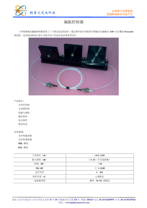
朗普达光电科技
让科研工作更高效 促进科技转化为生产力
偏振控制器
三环型机械式偏振控制器采用了三个固定延迟的波片,通过调节波片的角度可使输出光偏振态(SOP )完全覆盖Poincare 球表面。
灵活的结构设计便于安装不同工作波长的多种类型光纤。
产品特点:
全光纤结构 全金属结构 低插入损耗 操作简单 高可靠性 稳定性高
应用领域:
光纤传输系统 光纤传感领域 PDL 测试 PLC 测试
工作波长(nm ) 1310/1550 插入损耗(dB ) ≤0.05(不含连接器)
回损 (dB ) >60 PDL(dB) ≤ 0.05dB 适合光纤 G .652 尾纤长度(m ) 1或指定 连接器类型
裸纤、FC/PC 或指定。
1310nm
( 差 ± lf) 温 度 系 数 为 一 误 k1 其
4 8 / 、 即 当温度 为 x C( 5 . ( , ’ 2 C
附 近 ) , 敏 电阻 咀 值 R ( 时 热 T X)
k 为: 0
X > 2 5 l R一 X ) ( 一 g ( 一 X
4型蝶形外壳审, 8 内部 集 成 有 光 隔 离 器 、 敏 电阻 和光 功 率 监 测 热 及控 制 所需 的光 电二极 管 , 以 可 提 供 高 线性 、 低噪 声 、 功 率 ( 高 最 高 达 2 rW ) 激 光 输 出 。 ( ) 0 o 的 图 2 为 其内部 电路示 意 图
( 5 X )g0 5 2一 I .9 2
苴 官
值 见表 1 :
实 际
l , 脚之 间是热 敏 电阻 。 脚 2 当 温 度 为 2 5 C时 , 阻 值 为 1 k 其 0f l
应 用 中2
广播 与电视接 术 ・ O 2 ̄J 5期 2O - l l
维普资讯
【 提 要 】本 文 通 过 介 绍 A1 1P 激 光 器 的 构 成 . 折 了1 1 n 光 发 送 机 的 工 作 原 理 . 述 了 6] 分 0m 3 阐 其 中主 要 电路 的 设 计 , 要 性 能 参 数 的 测 试 , 时 指 出 在 设 计 . 产 和 使 用 光 发 这 机 时 的 注 意 主 同 生
它 主 要 由 前置 射 频 放大 电路 , 预 失 真 校正 电 路 . 自动 功 率 控 制
( C)电 路 ,自 动 温 度 控 制 AP
导体激 光器 是美 国朗讯 公 司专为 P D 制 有 线 电视 应 用 而 设 计 AI 一
生 产 的 。 封 装 _一 个 l 脚 OC 它 芷 4
UL1310中文版(电源方案下载请到以下网站下载)

UL1310ISB1-55989-589-6 CLASS 2 电源设备安全标准CLASS 2 POWER UNITS目录序文1.范围2.语汇3.组件4.总类装配5.机械集成6.外壳7.抗锈蚀8.开关9.保护装置10.组件11.线圈绝缘12.输入连接13.输出连接14.带电零件的可触性15.带电零件16.消除应变17.内部配线18.电路分隔19.绝缘材料20.印制电路板21.接地措施22.空间设计性能测试23.一般要求24.漏电测试25.暴露在潮湿环境下的漏电测试及耐压测试26.最大输出电压测试27.最大输入测试28.输出电流及电力测试29.防过载装置的校准测试30.全载输出电流测试31.正常温度测试32.耐压测试33.防过热和过载保护装置的耐久力测试34.重复耐压测试35.开关及操控装置的负载及耐久力测试36.次级开关的过载测试37.工作测试38.不正常测试39.绝缘材料测试40.消除应变测试40A.后推力消除测试41.直接插入铜脚固定测试42.输入接触的直接插入式固定测试43.输出连接器安全测试44.滥用测试45.接合导线测试制造及产品测试46.耐压测试47.接地连续性测试额定值48.总类标记49.详细资料规章50.使用手册附录一标准零件前言A.本标准乃根据Underwriters Laboratories Inc. (UL)对产品的基本要求作出以下的限制及标准范围。
此限制基于坚固的工程定理、研究、测试记录和经验,及与制造商、用户、检验部门和一些有特别经验的专业人士磋商及收取信息,解决制作过程及安装上的问题。
他们需要更多的经验和研究来不断求进。
B.由机械工程师观察本标准的要求是继续规范制造商的产品的其中一个状况。
C.若本标准被诊察和测试出有些会损害安全界限的情况,符合本标准原文的产品可以不需要被鉴定是否符合本标准。
D.使用有别于本标准列明的规条之材料或工作程序,可能会根据要求被诊察和测试。
若被发现在本质上大致相同,可能会被鉴定是否符合本标准。
电池充电器UL1310报告应当如何办理?
电池充电器UL1310报告应当如何办理?
亚马逊每隔一段时间就会揪出一批卖家索要相关的认证,在限期内提供不了,就会被下架Listing。
随着亚马逊美国站解除发货限制,不少
卖家因电子产品缺乏认证情况收到了邮件,美国站要求卖家提供UL认证,在规定的限期内提供不了就下架Listing。
UL1310用于检测电源设备,为电源设备安全标准。
电源设备在亚马逊上架需要办理UL1310报告。
UL1310认证测试项目如下:
1.泄漏电流测试
2.潮态处理后的泄露电流测试和介电耐压测试
3.输出电压测试
4. 输入测试
5.过流保护器件的校准
6.满载输出电流测
7.正常温度测试
8.耐压测试
9.感应电压测试
10.过流保护装置和过温度保护装置的耐久性测试
11.开关和控制器的过载和耐久性测试
12.次级开关的过载测试
13.操作测试
14.异常测试
15.绝缘材料测试
16.拉力测试
17.回推力测试
18.直插式设备插脚可靠性测试
19.直插式设备接触牢靠性测试
20.滥用测试
21.接地导体测试
22.应力释放测试
报告办理流程:
1、填写申请表
2、提交产品资料(BOM清单、说明书、电路图等)
3、快递样品
4、测试完成
5、出UL报告。
千兆光收发器参数
千兆光收发器参数
千兆光收发器通常用于高速数据传输应用,其参数包括以下几个方面:
1. 传输速率:千兆光收发器的传输速率通常为1Gbps,即每秒可以传输1GB的数据。
2. 波长范围:千兆光收发器一般支持850nm和1310nm两种波长,分别用于短距离和长距离传输。
3. 发射功率:发射功率是指光信号从光收发器发出时的光功率大小,一般在-9dBm到-3dBm之间。
4. 接收灵敏度:接收灵敏度是指光收发器在接收光信号时的最小光功率大小,一般在-19dBm到-14dBm之间。
5. 工作温度范围:千兆光收发器的工作温度范围一般为0℃到70℃之间。
6. 光纤接口类型:千兆光收发器的光纤接口类型包括LC、SC 和ST等,用户根据实际需求选择。
7. 适用网络类型:千兆光收发器适用于以太网、光纤通道等多种网络类型。
以上是千兆光收发器的主要参数,选择时需要根据实际需求进行合理搭配,以达到最佳性能和效果。
- 1 -。
LD、PD选型
PD按照封装类型分:
4pin 5pin带Isource或者Vpd 6pin带Vpd和RSSI
主要参数: 响应度Responsivity
灵敏度Sensitivity(PIN-TIA和APD-TIA)
饱和光功率Saturation Power 击穿电压Vapd(APD-TIA)
传输特性
发射 接收 速率 155M 1310FP PINTIA 1.25G 2.5G 1310FP/ 1550FP 155M PINTIA 1.25G … 距离/km(括号内不承诺) 40(60) 10(20) 2 20
LD、PD选型
——吴党辉
2012-08-09
芯片工艺及光电特性介绍PPT课件

2021/7/29
4
第4页/共43页
FP LD Wafer
P-InGaAs Contact layer P-InP Contact layer Etching Stop layer
Upper Confining layer MQW Active region Lower Confining layer N-InP Buffer Layer N-InP Substrate
2021/7/29
39
第39页/共43页
PD探针测试仪:主要用于PD芯片解理前测试筛选
2021/7/29
40
第40页/共43页
镀膜机
在LD两端面上镀光学膜,保证LD单面出光 F-P:保护膜和高反膜 DFB:增透膜和高反膜
2021/7/29
41
第41页/共43页
谢谢!
2021/7/29
42
第42页/共43页
剥离及 N 面 减薄
光刻制作 高频电极
N 面溅射 Ti/Pt/Au
光刻刻 蚀接触 条
合金
淀积绝缘 介质膜
光刻腐蚀 双沟波导 结构
解理为 bar 中测
解理为 chip
镀膜后的 抽样测试
蒸镀光学膜
镀膜前的 抽样老化
管芯
老化筛选
2021/7/29
封装
10
第10页/共43页
典型的BH-DFB LD制作工艺流程图
磨片机
在制作N面电极前将外延片减薄要求的厚度。
2021/7/29
33
第33页/共43页
合金炉
制作完P/N两面金属电极后,对芯片进行快速热处理的方式称 为合金,有利于形成平滑的接触面和良好的粘附特性,目的 是为了使管芯形成良好的欧姆接触特性。
数字三进1310+电流计及故障原因显示产品说明说明书
• Can be rotated to accommodate various breaker mounting orientations.
• LCD screen with a maximum of 8 characters.
• Reset button — clears display after trip.
• Scroll button to view ratings/functions — singlestep manual and automatic continuous scroll.
• TRIP LNG (long delay)
• TRIP MAG (instantaneous/short delay)
• LOAD<20% — display has switched to battery.
Customer Interface
• Status LED — flashes once every second to indicate the unit is functioning properly.
DESCRIPTION
Series G Ammeter and Cause of Trip Display
CATALOG NUMBER
DIGIVIEW
Eaton Electrical Inc. 1000 Cherrington Parkway Moon Township, PA 15108 United States tel: 1-800-525-2000
科技成果——大功率塑封脉冲半导体激光器
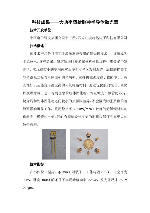
科技成果——大功率塑封脉冲半导体激光器技术开发单位中国电子科技集团公司十三所、石家庄麦特达电子科技有限公司技术概述该技术产品是目前工业激光测距采用的最先进技术,并逐渐成为主流技术。
该产品采用隧道结级联技术在材料外延过程中堆叠多个发光区,实现在较小的空间内实现多个发光区发射激光,成倍的提高半导体激光二极管单位面积的光功率。
选择机械强度高、收缩率小、透光性好以及热变形温度高的环氧树脂材料,通过优化胶的混合、固化以及烘烤等工艺,得到理想的胶体固化物,保证激光二极管的芯片、键合线和胶体固化物之间较小的热膨胀差异,不会因为膨胀系数的差异而影响可靠工作,采用导热率(398W/m•K)较好的无氧铜材料制作激光二极管的支架,同时合理地设计支架的形状以保证具有更大的散热面积。
技术指标在小体积(塑封、φ5mm)封装下,工作电流≤10A,占空比为0.1%、脉宽100ns的条件下实现峰值功率≥25W,发光区尺寸75μm ×1μm;在额定电流下,高温(55℃±3℃)工作时辐射功率与常温(25℃±3℃)工作时相比变化量≤10%;在额定电流下,低温(-40℃±3℃)工作时辐射功率与常温(25℃±3℃)工作时相比变化量≤10%。
技术特点为实现单个管芯具有较高的输出光功率,采用隧道结级联技术在材料外延过程中堆叠多个发光区,实现在较小的空间内实现多个发光区发射激光,成倍的提高半导体激光二极管单位面积的光功率。
先进程度国内先进技术状态批量生产、成熟应用阶段适用范围广泛应用于无人驾驶用车载激光雷达,危险、特殊环境下测距,以及电力、机械、狩猎、高尔夫球场、旅游观光等。
专利状态授权专利1项合作方式合作研发、技术服务;寻求投资扩大产能,大功率塑封激光器生产线产能达到10万支/年,资金需求200万元,实施周期36个月。
预期效益目前脉冲激光测距在国内市场的需求量约50万只/每年,市场价30元/只以上,市场销量可达到1500万元以上。
- 1、下载文档前请自行甄别文档内容的完整性,平台不提供额外的编辑、内容补充、找答案等附加服务。
- 2、"仅部分预览"的文档,不可在线预览部分如存在完整性等问题,可反馈申请退款(可完整预览的文档不适用该条件!)。
- 3、如文档侵犯您的权益,请联系客服反馈,我们会尽快为您处理(人工客服工作时间:9:00-18:30)。
Optoway
InGaAs PIN PD MODULES
InGaAs PIN PHOTODIODE WITH SINGLE-MODE FIBER PIGTAIL FEATURES
² ² ² ² ² High responsivity for dual windows at 1310 nm and 1550 nm Low dark current Quick pulse response Low return loss Coaxial Module with 9/125 µm Single-Mode Fiber (PD-1310)
OPTOWAY TECHNOLOGY INC. No.38, Kuang Fu S. Road, Hu Kou, Hsin Chu Industrial Park, Hsin Chu, Taiwan 303
Tel: 886-3-5979798 E-mail: sales@ Fax:886-3-5979737 http: // 1/3/2002 V1.0
****************************************************************************************************************************************************************
ELECTRICAL AND OPTICAL CHARACTERISTICS (Tc=25ºC)
Symbol Parameter Detection Range R Responsivity λ VR=5V, λ=1300nm VR=5V, λ=1550nm Idark C Tr/Tf ORL BW Dark Current Capacitance Rise/Fall Time Optical Return Loss Bandwidth VR=5V VR=5V VR=5V, 10~90% VR=5V, λ=1300nm VR=5V 40 2 Test Conditions Min. 1100 0.85 0.90 0.3 0.7 Typ. Max. 1650 0.7 1.0 0.5 Unit nm A/W A/W nA pF ns dB GHz
元器件交易网
Optoway
MECHANICAL DIMENSION (mm) and PIN ASSIGNMENT
PD-1310
****************************************************************************************************************************************************************
PD-1310
****************************************************************************************************************************************************************
OPTOWAY TECHNOLOGY INC. No.38, Kuang Fu S. Road, Hu Kou, Hsin Chu Industrial Park, Hsin Chu, Taiwan 303
Tel: 886-3-5979798 E-mail: sales@ Fax:886-3-5979737 http: // 1/3/2002 V1.0
****************************************************************************************************************************************************************
Absolute Maximum Ratings (Tc=25 ºC)
Symbol Po VRD IFD Topr Tstg Parameter Input Optical Power PD Reverse Voltage PD Forward Current Operating Temperature Storage Temperature Ratings 10 20 10 -40~+85 -40~+85 Unit mW V mA ºC ºC
Code 0 1 2 Code V H X Fiber 50/125 µm 9/125 µm 62.5/125 µm Flange Vertical Horizontal No Flange
□ □
Code S F T X SA FA Connector Type SC/PC FC/PC ST/PC No Connector SC/APC FC/APC
APPLICATION
SDH, ATM, LAN
DESCRIPTION
PD-1310 series are designed for coupling a single-mode fiber with high reliable InGaAs PIN photodiodes. PD-1310 series are specially designed as detector for Datacom and Telecom application.
Note: 1. Specifications subject to change without notice. 2. Other PIN assignment is available upon request.
ORDER INFORMATION
Part No.: P D − 1 3 □ 0 − □
PD-1310
****************************************************************************************************************************************************************