K9F1G08U0M单板测试资料
K9F1G08UOM数据手册

m A 5 5 15 15 1 10 10 20 20 1 µA 10 50 10 50
页 编 ICC2 程 擦除 ICC3 ISB1 等待状态电流 (TTL) 等待状态电流 (CMOS) 输入开漏电流 输出开漏电流
ISB2
IL1 IL0
-
-
±10 ±10
-
-
±10 ±10 VCC V +0.3 0.8 -
6. 命令/地址/ 数据复用端口: 7. 硬件数据保护:编程/擦除操作在电源转换时关闭。 8. 可靠的 CMOS 浮置门技术: --保证:100K 编程/ 擦除次数。 --数据保持时间: 10 年。 9. 命令寄存器操作 10. 为高速编程设置的缓冲编程操作。 11. 通电自动读操作。 12. 智能复制拷贝操作。 13.为防盗版而设置的唯一的 ID 保护。 14. 封装。 - K9F1GXXX0M-YCB0/YIB0 48 - Pin TSOP I (12 x 20 / 0.5 mm pitch) - K9F1G08U0M-VCB0/VIB0 48 - Pin WSOP I (12X17X0.7mm)
器件描述
三星 K9F1GXXX0M 提供了 128M*8Bit/64M*16Bit 的存储容量,另外还有 32 M 的空闲存储器,它是采用 NAND 技术的大容量、高可靠的 Flash 存储器。 它对 2112 字节一页(*8device )或者 1056 字(*16device)一页的写操作。典型 时间是 300 微秒。对 128 字节/64K 字一块的擦除时间是 50 纳秒。输出引脚可 以作为数据/地址/命令复用。每一页的数据读出时间也很快,平均每个字节只 需 50 纳秒。片内的写控制器,可以自动执行写操作和擦除功能,包括必要的脉 冲产生器,内部校验和冗余数据。 K9F1G08 提供了实时映像算法的纠错码,写 操作系统可以利用 K9F1G08U0M 扩展的 100K 编程/ 擦除。K9F1G08U0M 为大 容量存储,新型电可擦写的非易失性半导体存储器,提供了最优方案。
MEMORY存储芯片K9F1G08U0B-PCB0中文规格书

Product IntroductionThe K9F1G08U0B is a 1,056Mbit(1,107,296,256 bit) memory organized as 65,536 rows(pages) by 2,112x8 columns. Spare 64x8 col-umns are located from column address of 2,048~2,111. A 2,112-byte data register is connected to memory cell arrays accommodat-ing data transfer between the I/O buffers and memory during page read and page program operations. The memory array is made up of 32 cells that are serially connected to form a NAND structure. Each of the 32 cells resides in a different page. A block consists of two NAND structured strings. A NAND structure consists of 32 cells. Total 1,081,344 NAND cells reside in a block. The program and read operations are executed on a page basis, while the erase operation is executed on a block basis. The memory array consists of 1,024 separately erasable 128K-byte blocks. It indicates that the bit by bit erase operation is prohibited on the K9F1G08U0B.The K9F1G08U0B has addresses multiplexed into 8 I/Os. This scheme dramatically reduces pin counts and allows system upgrades to future densities by maintaining consistency in system board design. Command, address and data are all written through I/O's by bringing WE to low while CE is low. Those are latched on the rising edge of WE. Command Latch Enable(CLE) and Address Latch Enable(ALE) are used to multiplex command and address respectively, via the I/O pins. Some commands require one bus cycle. For example, Reset Command, Status Read Command, etc require just one cycle bus. Some other commands, like page read and block erase and page program, require two cycles: one cycle for setup and the other cycle for execution. The 132M byte physical space requires 28 addresses, thereby requiring four cycles for addressing : 2 cycles of column address, 2 cycles of row address, in that order. Page Read and Page Program need the same four address cycles following the required command input. In Block Erase oper-ation, however, only the two row address cycles are used. Device operations are selected by writing specific commands into the com-mand register. Table 1 defines the specific commands of the K9F1G08U0B.In addition to the enhanced architecture and interface, the device incorporates copy-back program feature from one page to another page without need for transporting the data to and from the external buffer memory. Since the time-consuming serial access and data-input cycles are removed, system performance for solid-state disk application is significantly increased.Table 1. Command SetsNOTE : 1. Random Data Input/Output can be executed in a page.2. Read EDC Status is only available on Copy Back operation.Caution : Any undefined command inputs are prohibited except for above command set of Table 1.Function1st Cycle 2nd CycleAcceptable Command during BusyRead00h 30h Read for Copy Back 00h 35h Read ID 90h -Reset FFh -OPage Program 80h 10h Copy-Back Program 85h 10h Block Erase60h D0h Random Data Input (1)85h -Random Data Output (1)05h E0hRead Status 70h O Read EDC Status (2)7BhODC AND OPERATING CHARACTERISTICS (Recommended operating conditions otherwise noted.)NOTE : 1. V IL can undershoot to -0.4V and V IH can overshoot to V CC +0.4V for durations of 20 ns or less.2. Typical value is measured at Vcc=3.3V, T A =25°C. Not 100% tested.ParameterSymbol Test ConditionsK9F1G08U0B(3.3V)UnitMinTypMaxOperating CurrentPage Read with Serial Access I CC 1tRC=25nsCE=V IL, I OUT =0mA-1530mAProgram I CC 2-EraseI CC 3-Stand-by Current(TTL)I SB 1CE=V IH , WP=0V/V CC --1Stand-by Current(CMOS)I SB 2CE=V CC -0.2, WP=0V/V CC -1050µAInput Leakage Current I LI V IN =0 to Vcc(max)--±10Output Leakage Current I LO V OUT =0 to Vcc(max)--±10Input High VoltageV IH (1)-0.8xVcc -V CC +0.3V Input Low Voltage, All inputs V IL (1)--0.3-0.2xVccOutput High Voltage Level V OH K9F1G08U0A :I OH =-400µA 2.4--Output Low Voltage Level V OLK9F1G08U0A :I OL =2.1mA--0.4Output Low Current(R/B)I OL (R/B)K9F1G08U0A :V OL =0.4V810-mA RECOMMENDED OPERATING CONDITIONS(Voltage reference to GND, K9F1G08U0B-XCB0 :T A =0 to 70°C, K9F1G0808B-XIB0:T A =-40 to 85°C)ParameterSymbol K9F1G08U0B(3.3V)UnitMin Typ.Max Supply Voltage V CC 2.7 3.3 3.6V Supply VoltageV SSV ABSOLUTE MAXIMUM RATINGSNOTE :1. Minimum DC voltage is -0.6V on input/output pins. During transitions, this level may undershoot to -2.0V for periods <30ns. Maximum DC voltage on input/output pins is V CC +0.3V which, during transitions, may overshoot to V CC +2.0V for periods <20ns.2. Permanent device damage may occur if ABSOLUTE MAXIMUM RATINGS are exceeded. Functional operation should be restricted to the conditions as detailed in the operational sections of this data sheet. Exposure to absolute maximum rating conditions for extended periods may affect reliability.ParameterSymbol Rating Unit3.3V Device Voltage on any pin relative to VSSV CC-0.6 to + 4.6VV IN -0.6 to + 4.6V I/O-0.6 to Vcc + 0.3 (< 4.6V)Temperature Under BiasK9XXG08XXB-XCB0T BIAS -10 to +125°C K9XXG08XXB-XIB0-40 to +125Storage Tempera-tureK9XXG08XXB-XCB0T STG-65 to +150°CK9XXG08XXB-XIB0Short Circuit CurrentI OS5mACAPACITANCE (T A =25°C, V CC =3.3V, f=1.0MHz)NOTE : Capacitance is periodically sampled and not 100% tested.ItemSymbol Test ConditionMin Max Unit Input/Output Capacitance C I/O V IL =0V -10pF Input CapacitanceC INV IN =0V-10pFVALID BLOCKNOTE :1. The device may include initial invalid blocks when first shipped. Additional invalid blocks may develop while being used. The number of valid blocks is presented with both cases of invalid blocks considered. Invalid blocks are defined as blocks that contain one or more bad bits. Do not erase or pro-gram factory-marked bad blocks. Refer to the attached technical notes for appropriate management of invalid blocks.2. The 1st block, which is placed on 00h block address, is guaranteed to be a valid block up to 1K program/erase cycles with 1bit/512Byte ECC.ParameterSymbol Min Typ.Max Unit K9F1G08U0BN VB1,004-1,024BlocksMODE SELECTIONNOTE : 1. X can be V IL or V IH.2. WP should be biased to CMOS high or CMOS low for standby.CLE ALE CE WERE WP ModeH L L H X Read Mode Command Input L H L H X Address Input(4clock)H L L H H Write ModeCommand Input L H L H H Address Input(4clock)L L L HH Data Input L L L H XData Output X X X X H X During Read(Busy)X X X X X H During Program(Busy)X X X X X H During Erase(Busy)X X (1)X X X L Write Protect XXHXX0V/V CC (2)Stand-byAC TEST CONDITION(K9F1G08U0B-XCB0 :TA=0 to 70°C, K9F1G08U0B-XIB0:TA=-40 to 85°C, K9F1G08U0B : Vcc=2.7V~3.6V unless otherwise noted)ParameterK9F1G08U0B Input Pulse Levels 0V to Vcc Input Rise and Fall Times 5ns Input and Output Timing Levels Vcc/2Output Load1 TTL GATE and CL=50pF。
K9F1G08U0E 存储器

K9F1G08U0ERev. 1.11, Aug. 2013SAMSUNG ELECTRONICS RESERVES THE RIGHT TO CHANGE PRODUCTS, INFORMATION AND SPECIFICATIONS WITHOUT NOTICE.Products and specifications discussed herein are for reference purposes only. All information discussed herein is provided on an "AS IS" basis, without warranties of any kind.This document and all information discussed herein remain the sole and exclusive property of Samsung Electronics. No license of any patent, copyright, mask work, trademark or any other intellectual property right is granted by one party to the other party under this document, by implication, estoppel or other-wise.Samsung products are not intended for use in life support, critical care, medical, safety equipment, or similar applications where product failure could result in loss of life or personal or physical harm, or any military or defense application, or any governmental procurement to which special terms or provisions may apply.For updates or additional information about Samsung products, contact your nearest Samsung office.All brand names, trademarks and registered trademarks belong to their respective owners.ⓒ2013 Samsung Electronics Co., Ltd. All rights reserved.SAMSUNG CONFIDENTIAL1Gb E-die NAND FlashSingle-Level-Cell (1bit/cell)datasheetRevision HistoryRevision No.History Draft Date Remark Edited by Reviewed by0.0 1. Initial issue Dec. 17, 2012Target H.K.Kim H.H.Shin0.01 1. Typo corrected. Feb.02, 2013Target H.K.Kim H.H.ShinFeb.22, 2013Target H.K.Kim H.H.Shin0.1Chapter 4.3 Input Data Latch CycleChapter 4.11 Copy-Back Program Operation with Random Data Inputrevised.1.0 1. read ID revised Jul.03, 2013Final S.M.Lee H.H.Shin1.1 1. Corrected errata Aug.06, 2013Final S.M.Lee H.H.Shin1.11 1. Industrial product feature added Aug.07, 2013Final S.M.Lee H.H.ShinTable Of Contents1.0 INTRODUCTION (4)1.1 General Description (4)1.2 Features (4)1.3 General Description (4)1.4Pin Configuration (TSOP1) (5)1.4.1 Package Dimensions (5)1.5 Pin Configuration (FBGA) (6)1.5.1 Package Dimensions (7)1.6 Pin Description (8)2.0 PRODUCT INTRODUCTION (10)2.1 Absolute Maximum Ratings (11)2.2 Recommended Operating Conditions (11)2.3 DC And Operating Characteristics(Recommended operating conditions otherwise noted.) (11)2.4 Valid Block (12)2.5 AC Test Condition (12)2.6 Capacitance(TA=25°C, VCC=3.3V, f=1.0MHz) (12)2.7 Mode Selection (12)2.8 Program / Erase Characteristics (13)2.9 AC Timing Characteristics for Command / Address / Data Input (13)2.10 AC Characteristics for Operation (14)3.0 NAND FLASH TECHNICAL NOTES (15)3.1 Initial Invalid Block(s) (15)3.2 Identifying Initial Invalid Block(s) (15)3.3 Error in Write or Read Operation (16)3.4 Addressing for Program Operation (18)4.0 SYSTEM INTERFACE USING CE DON’T-CARE (19)4.1 Command Latch Cycle (20)4.2 Address Latch Cycle (20)4.3 Input Data Latch Cycle (21)4.4 Status Read Cycle (22)4.5 Read Operation (23)4.6 Read Operation(Intercepted by CE) (23)4.7 Random Data Output In a Page (24)4.8 Page Program Operation (25)4.9 Page Program Operation with Random Data Input (26)4.10 Copy-Back Program Operation (27)4.11 Copy-Back Program Operation with Random Data Input (28)4.12 Block Erase Operation (29)4.13 Read ID Operation (29)5.0 DEVICE OPERATION (32)5.1 Page Read (32)5.2 Page Program (33)5.3 Copy-Back Program (34)5.4 Block Erase (35)5.5 Read Status (35)5.6 Read ID (36)5.7 Reset (36)5.8 Ready/busy (37)6.0 DEVICE OPERATION (38)1.0 INTRODUCTION1.1 General Description1.2 Features1.3 General DescriptionOffered in 128Mx8bit, the K9F1G08U0E is a 1G-bit NAND Flash Memory with spare 32M-bit. Its NAND cell provides the most cost-effective solution for the solid state application market. A program operation can be performed in typical 400μs on the (2K+64)Byte page and an erase operation can be per-formed in typical 4.5ms on a (128K+4K)Byte block. Data in the data register can be read out at 25ns cycle time per Byte. The I/O pins serve as the ports for address and data input/output as well as command input. The on-chip write controller automates all program and erase functions including pulse rep-etition, where required, and internal verification and margining of data. Even the write-intensive systems can take advantage of the K9F1G08U0E 's extended reliability by providing ECC(Error Correcting Code) with real time mapping-out algorithm. The K9F1G08U0E is an optimum solution for large nonvolatile storage applications such as solid state file storage and other portable app.lications requiring non-volatility.Part Number Vcc Range OrganizationPKG Type K9F1G08U0E-S 2.7V ~ 3.6V x8TSOP1K9F1G08U0E-B2.7V ~3.6Vx863FBGA∙ Voltage Supply- 3.3V Device(K9F1G08U0E) : 2.7V ~ 3.6V ∙ Organization- Memory Cell Array : (128M + 4M) x 8bit - Data Register : (2K + 64) x 8bit ∙ Automatic Program and Erase - Page Program : (2K + 64)Byte - Block Erase : (128K + 4K)Byte ∙ Page Read Operation- Page Size : (2K + 64)Byte - Random Read : 40μs(Max.) - Serial Access : 25ns(Min.)∙ Fast Write Cycle Time- Page Program time : 400μs(Typ.) - Block Erase Time : 4.5ms(Typ.)∙ Command/Address/Data Multiplexed I/O Port ∙ Hardware Data Protection- Program/Erase Lockout During Power Transitions ∙ Reliable CMOS Floating-Gate Technology-Endurance & Data Retention : Refor to the gualification report -ECC regnirement : 1 bit / 528bytes ∙ Command Driven Operation∙ Unique ID for Copyright Protection ∙ Package :- K9F1G08U0E-SCB0/SIB0 : Pb-FREE PACKAGE 48 - Pin TSOP I (12 x 20 / 0.5 mm pitch)- K9F1G08U0E-BCB0/BIB0 : Pb-FREE PACKAGE 63 FBGA (9 x 11 / 0.8 mm pitch)K9F1G08U0E-SCB0/SIB048-pin TSOP1Standard Type 12mm x 20mm123456789101112131415161718192021222324484746454443424140393837363534333231302928272625N.C N.C N.C N.C N.C N.C R/B RE CE N.C N.C Vcc Vss N.C N.C CLE ALE WE WP N.C N.C N.C N.C N.CN.C N.C N.C N.C I/O7I/O6I/O5I/O4N.C N.C N.C Vcc Vss N.C N.C N.C I/O3I/O2I/O1I/O0N.C N.C N.C N.C1.4.1 Package Dimensions48-PIN LEAD FREE PLASTIC THIN SMALL OUT-LINE PACKAGE TYPE(I)48 - TSOP1 - 1220AFUnit :mm/Inch0.787±0.00820.00±0.20#1#240.16+0.07-0.030.008+0.003-0.0010.500.0197#48#250.48812.40M A X12.000.4720.10 0.004M A X 0.250.010()0.039±0.0021.00±0.050.0020.05MIN0.0471.20MAX0.45~0.750.018~0.0300.724±0.00418.40±0.100~8︒0.0100.25T Y P0.125+0.0750.0350.005+0.003-0.0010.500.020()0.20+0.07-0.03K9F1G08U0E-BCB0/BIB0R/B /WE /CE Vss ALE /WP /RE CLE NC NC NC NC Vcc NC NC I/O0I/O1NC NCVccI/O5I/O7VssI/O6I/O4I/O3I/O2VssNC NC NC NC NC NC NC NC NC NC NC NC NC NC NC NC NCNC NC NCN.CN.C N.C N.C N.C N.C N.CN.CN.C N.C N.C N.CN.C N.C N.C Top View78910563412A B C D G E F H J K L M1.5.1 Package Dimensions9.00±0.10#A111.00±0.100.32±0.050.90±0.100.10 M A X4321A B C D G 63-∅0.45±0.059.00±0.10(Datum B)0.2 M A B∅0.80 x 11= 8.80 0.80 x 9= 7.2065E F H J K L M(Datum A)871090.800.403.600.800.404.4011.00±0.10A#A1 INDEX MARKB63-Ball FBGA (measured in millimeters)TOP VIEW SIDE VIEW BOTTOM VIEW1.6 Pin DescriptionNOTE :Connect all VCC and VSS pins of each device to common power supply outputs.Pin Name Pin FunctionI/O 0 ~ I/O 7DATA INPUTS/OUTPUTSThe I/O pins are used to input command, address and data, and to output data during read operations. The I/O pins float to high-z when the chip is deselected or when the outputs are disabled.CLECOMMAND LATCH ENABLEThe CLE input controls the activating path for commands sent to the command register. When active high, commands are latched into the command register through the I/O ports on the rising edge of the WE signal.ALEADDRESS LATCH ENABLEThe ALE input controls the activating path for address to the internal address registers. Addresses are latched on the rising edge of WE with ALE high.CECHIP ENABLEThe CE input is the device selection control. When the device is in the Busy state, CE high is ignored, and the device does not return to standby mode in program or erase operation.REREAD ENABLEThe RE input is the serial data-out control, and when active drives the data onto the I/O bus. Data is valid tREA after the fall-ing edge of RE which also increments the internal column address counter by one.WEWRITE ENABLEThe WE input controls writes to the I/O port. Commands, address and data are latched on the rising edge of the WE pulse.WPWRITE PROTECTThe WP pin provides inadvertent program/erase protection during power transitions. The internal high voltage generator is reset when the WP pin is active low.R/BREADY/BUSY OUTPUTThe R/B output indicates the status of the device operation. When low, it indicates that a program, erase or random read operation is in process and returns to high state upon completion. It is an open drain output and does not float to high-z con-dition when the chip is deselected or when outputs are disabled.Vcc POWERV CC is the power supply for device. Vss GROUNDN.CNO CONNECTION[Figure 1] K9F1G08U0E Functional Block Diagram[Figure 2] K9F1G08U0E Array OrganizationNOTE :Column Address : Starting Address of the Register.* L must be set to "Low".* The device ignores any additional input of address cycles than required.I/O 0I/O 1I/O 2I/O 3I/O 4I/O 5I/O 6I/O 71st Cycle A 0A 1A 2A 3A 4A 5A 6A 72nd Cycle A 8A 9A 10A 11*L *L *L *L 3rd Cycle A 12A 13A 14A 15A 16A 17A 18A 194th CycleA 20A 21A 22A 23A 24A 25A 26A 27V CC X-Buffers Command I/O Buffers & LatchesLatches & Decoders Y-Buffers Latches & DecodersRegisterControl Logic & High Voltage GeneratorGlobal BuffersOutput DriverV SSA 12 - A 27A 0 - A 11CommandCE RE WE CLE WPI/0 0I/0 7V CC V SSALE 1,024M + 32M Bit NAND Flash ARRAY (2,048 + 64)Byte x 65,536Y-GatingData Register & S/A1 Page = (2K + 64)Bytes1 Block = (2K + 64)B x 64 Pages = (128K + 4K) Bytes1 Device = (2K+64)B x 64Pages x 1,024 Blocks = 1,056 MbitsRow Address Row AddressColumn Address Column Address2.0 PRODUCT INTRODUCTIONNAND Flash Memory has addresses multiplexed into 8 I/Os. This scheme dramatically reduces pin counts and allows system upgrades to future densities by maintaining consistency in system board design. Command, address and data are all written through I/O's by bringing WE to low while CE is low. Those are latched on the rising edge of WE. Command Latch Enable(CLE) and Address Latch Enable(ALE) are used to multiplex command and address respectively, via the I/O pins. Some commands require one bus cycle. For example, Reset Command, Status Read Command, etc. require just one cycle bus. Some other commands, like page read and block erase and page program, require two cycles: one cycle for setup and the other cycle for execution.. Page Read and Page Program need the same four address cycles following the required command input. In Block Erase operation, however, only the two row address cycles are used. Device operations are selected by writing specific commands into the command register. Table 1 defines the specific com-mands of the K9F1G08U0E.[Table 1] Command SetsFunction1st Cycle2nd Cycle Acceptable Command during BusyRead 00h30hRead for Copy Back00h35hRead ID90h-Reset FFh-OPage Program80h10hCopy-Back Program85h10hBlock Erase60h D0hRandom Data Input(1)85h-Random Data Output(1)05h E0hRead Status70h-ONOTE :1) Random Data Input/Output can be executed in a page.Caution :Any undefined command inputs are prohibited except for above command set of Table 1.2.1 Absolute Maximum RatingsNOTE :1) Minimum DC voltage is -0.6V on input/output pins. During transitions, this level may undershoot to -2.0V for periods <30ns. Maximum DC voltage on input/output pins is V CC +0.3V which, during transitions, may overshoot to V CC +2.0V for periods <20ns.2) Permanent device damage may occur if ABSOLUTE MAXIMUM RATINGS are exceeded. Functional operation should be restricted to the conditions as detailed in the operational sections of this data sheet. Exposure to absolute maximum rating conditions for extended periods may affect reliability.2.2 Recommended Operating Conditions(Voltage reference to GND, K9F1G08U0E-SCB0 :T A =0 to 70︒C, K9F1G08U0E-XIB0:T A =-40 to 85︒C)2.3 DC And Operating Characteristics (Recommended operating conditions otherwise noted.)NOTE :1) V IL can undershoot to -0.4V and V IH can overshoot to V CC +0.4V for durations of 20 ns or less 2) Typical value is measured at Vcc=3.3V, T A =25︒C. Not 100% tested.ParameterSymbol Rating Unit Voltage on any pin relative to VSSV CC -0.6 to + 4.6V V IN -0.6 to + 4.6V I/O-0.6 to Vcc + 0.3 (< 4.6V)Temperature Under Bias K9F1G08U0E-xCB0T BIAS -10 to +125︒C K9F1G08U0E-xIB0-40 to +125 Storage Temperature K9F1G08U0E-xCB0/xIB0T STG-65 to +150︒CShort Circuit CurrentI OS5mAParameterSymbol K9F1G08U0E(3.3V)Unit Min Typ.Max Supply Voltage V CC 2.7 3.3 3.6V Supply VoltageV SSVParameterSymbol Test ConditionsK9F1G08U0E(3.3V)UnitMinTypMaxOperating CurrentPage Read with Serial Access I CC 1tRC=25nsCE=V IL, I OUT =0mA-2035mAProgram I CC 2-EraseI CC 3-Stand-by Current(TTL)I SB 1CE=V IH , WP=0V/V CC --1Stand-by Current(CMOS)I SB 2CE=V CC -0.2, WP=0V/V CC -1080μAInput Leakage Current I LI V IN =0 to Vcc(max)--±10Output Leakage Current I LO V OUT =0 to Vcc(max)--±10Input High VoltageV IH (1)-0.8xVcc -V CC +0.3V Input Low Voltage, All inputs V IL (1)--0.3-0.2XVccOutput High Voltage Level V OH K9F1G08U0E :I OH =-400μA 2.4--Output Low Voltage Level V OL K9F1G08U0E :I OL =2.1mA --0.4Output Low Current(R/B)I OL (R/B)K9F1G08U0E :V OL =0.4V810-mA2.4 Valid BlockParameter Symbol Min Typ.Max UnitK9F1G08U0E N VB1,004-1,024BlocksNOTE :1) The device may include initial invalid blocks when first shipped. Additional invalid blocks may develop while being used. The number of valid blocks is presented with bothcases of invalid blocks considered. Invalid blocks are defined as blocks that contain one or more bad bits. Do not erase or program factory-marked bad blocks. Refer to the attached technical notes for appropriate management of invalid blocks.2) The 1st block, which is placed on 00h block address, is guaranteed to be a valid block up to 1K program/erase cycles with 1bit/528Byte ECC.2.5 AC Test Condition(K9F1G08U0E-XCB0 :TA=0 to 70︒C, K9F1G08U0E-XIB0:TA=-40 to 85︒C, K9F1G08U0E : Vcc=2.7V~3.6V unless otherwise noted)Parameter K9F1G08U0EInput Pulse Levels0V to VccInput Rise and Fall Times5nsInput and Output Timing Levels Vcc/2Output Load 1 TTL GATE and CL=50pF2.6 Capacitance(TA=25︒C, VCC=3.3V, f=1.0MHz)Item Symbol Test Condition Min Max UnitInput/Output Capacitance C I/O V IL=0V-10pFInput Capacitance C IN V IN=0V-10pFNOTE :Capacitance is periodically sampled and not 100% tested.2.7 Mode SelectionNOTE :1) X can be V IL or V IH.2) WP should be biased to CMOS high or CMOS low for standby.2.8Program / Erase CharacteristicsParameter Symbol Min Typ Max Unit Program Time t PROG-400900μs Number of Partial Program Cycles Nop--1cycles Block Erase Time t BERS- 4.516ms NOTE :1) Typical value is measured at Vcc=3.3V, T A=25︒C. Not 100% tested.2) Typical program time is defined as the time within which more than 50% of the whole pages are programmed at 3.3V Vcc and 25︒C temperature.2.9 AC Timing Characteristics for Command / Address / Data InputParameter Symbol Min Max Unit CLE Setup Time t CLS(1)12-ns CLE Hold Time t CLH5-ns CE Setup Time t CS(1)20-ns CE Hold Time t CH5-ns WE Pulse Width t WP12-ns ALE Setup Time t ALS(1)12-ns ALE Hold Time t ALH5-ns Data Setup Time t DS(1)12-ns Data Hold Time t DH5-ns Write Cycle Time t WC25-ns WE High Hold Time t WH10-ns Address to Data Loading Time t ADL(2)100-ns NOTE :1) The transition of the corresponding control pins must occur only once while WE is held low2) tADL is the time from the WE rising edge of final address cycle to the WE rising edge of first data cycle2.10AC Characteristics for OperationParameter Symbol Min Max Unit Data Transfer from Cell to Register t R-40μs ALE to RE Delay t AR10-ns CLE to RE Delay t CLR10-ns Ready to RE Low t RR20-ns RE Pulse Width t RP12-ns WE High to Busy t WB-100ns Read Cycle Time t RC25-ns RE Access Time t REA-20ns CE Access Time t CEA-25ns RE High to Output Hi-Z t RHZ-100ns CE High to Output Hi-Z t CHZ-30ns CE High to ALE or CLE Don’t Care t CSD0-ns RE High to Output Hold t RHOH15-ns CE High to Output Hold t COH15-ns RE High Hold Time t REH10-ns Output Hi-Z to RE Low t IR0-ns RE High to WE Low t RHW100-ns WE High to RE Low t WHR60-ns Device Resetting Time(Read/Program/Erase)t RST-5/10/500(1)μs NOTE :1) If reset command(FFh) is written at Ready state, the device goes into Busy for maximum 5μs.3.0 NAND FLASH TECHNICAL NOTES3.1 Initial Invalid Block(s)Initial invalid blocks are defined as blocks that contain one or more initial invalid bits whose reliability is not guaranteed by Samsung. The information regarding the initial invalid block(s) is called the initial invalid block information. Devices with initial invalid block(s) have the same quality level as devices with all valid blocks and have the same AC and DC characteristics. An initial invalid block(s) does not affect the performance of valid block(s) because it is isolated from the bit line and the common source line by a select transistor. The system design must be able to mask out the initial invalid block(s) via address mapping. The 1st block, which is placed on 00h block address, is guaranteed to be a valid block up to 1K program/erase cycles with 1bit /528Byte ECC.3.2 Identifying Initial Invalid Block(s)All device locations are erased(FFh) except locations where the initial invalid block(s) information is written prior to shipping. The initial invalid block(s) status is defined by the 1st byte in the spare area. Samsung makes sure that either the 1st or 2nd page of every initial invalid block has non-FFh data at the column address of 2048. Since the initial invalid block information is also erasable in most cases, it is impossible to recover the information once it has been erased. Therefore, the system must be able to recognize the initial invalid block(s) based on the original initial invalid block information and create the initial invalid block table via the following suggested flow chart(Figure 3). Any intentional erasure of the original initial invalid block information is pro-hibited.[Figure 3] Flow chart to create initial invalid block table*Check "FFh" at the column address 2048 StartSet Block Address = 0Check "FFh"Increment Block AddressLast Block ?EndNoYesYesCreate (or update)NoInitialof the 1st and 2nd page in the blockInvalid Block(s) Table3.3 Error in Write or Read OperationWithin its life time, additional invalid blocks may develop with NAND Flash memory. Refer to the qualification report for the actual data.The following pos-sible failure modes should be considered to implement a highly reliable system. In the case of status read failure after erase or program, block replace-ment should be done. Because program status fail during a page program does not affect the data of the other pages in the same block, blockreplacement can be executed with a page-sized buffer by finding an erased empty block and reprogramming the current target data and copying the rest of the replaced block. In case of Read, ECC must be employed. To improve the efficiency of memory space, it is recommended that the read or verifica-tion failure due to single bit error be reclaimed by ECC without any block replacement. The said additional block failure rate does not include those reclaimed blocks.ECC : Error Correcting Code --> Hamming Code etc.Example) 1bit correction & 2bit detectionProgram Flow ChartFailure ModeDetection and Countermeasure sequenceWrite Erase Failure Status Read after Erase --> Block Replacement Program Failure Status Read after Program --> Block Replacement ReadSingle Bit FailureVerify ECC -> ECC CorrectionStartI/O 6 = 1 ?I/O 0 = 0 ?No*Write 80hWrite AddressWrite DataWrite 10hRead Status RegisterProgram Completedor R/B = 1 ?YesNoYes: If program operation results in an error, map out the block including the page in error and copy thetarget data to another block.*NAND Flash Technical Notes (Continued)* Step1When an error happens in the nth page of the Block ’A’ during erase or program operation. * Step2Copy the data in the 1st ~ (n-1)th page to the same location of another free block. (Block ’B’)* Step3Then, copy the nth page data of the Block ’A’ in the buffer memory to the nth page of the Block ’B’.* Step4Do not erase or program to Block ’A’ by creating an ’invalid block’ table or other appropriate scheme.Erase Flow ChartStartI/O 6 = 1 ?I/O 0 = 0 ?No*Write 60h Write Block AddressWrite D0h Read Status Registeror R/B = 1 ?Erase ErrorYesNo: If erase operation results in an error, map out the failing block and replace it with another block.* Erase CompletedYesRead Flow ChartBlock Replacement1st Block Anth 1st nth3.4 Addressing for Program OperationWithin a block, the pages must be programmed consecutively from the LSB(least significant bit) page of the block to the MSB(most significant bit) pages of the block. Random page address programming is prohibited. In this case, the definition of LSB page is the LSB among the pages to be programmed. Therefore, LSB doesn't need to be page 0.From the LSB page to MSB page DATA IN: Data (1)Data (64)(1)(2)(3)(32)(64)Data register Page 0Page 1Page 2Page 31Page 63::4.0 SYSTEM INTERFACE USING CE DON’T-CARE.For an easier system interface, CE may be inactive during the data-loading or serial access as shown below. The internal 2,112byte data registers are utilized as separate buffers for this operation and the system design gets more flexible. In addition, for voice or audio applications which use slow cycle time on the orde[Figure 5] Read Operation with CE don’t-care.Address InformationDevice I/O DATA ADDRESSI/Ox Data In/Out Col. Add1Col. Add2Row Add1Row Add2K9F1G08U0EI/O 0 ~ I/O 7~2112byteA0~A7A8~A11A12~A19A20~A27CLE≈≈≈Address(4Cycle)00h ALE WEData Output(serial access)R/BtRE 30h I/Ox≈≈≈≈4.1 Command Latch Cycle4.2 Address Latch CycleCEWECLEALEI/OxCEWECLEALEI/Ox4.3 Input Data Latch CycleCECLEWEALEI/Ox* Serial Access Cycle after Read (CLE=L, WE=H, ALE=L)NOTE :Transition is measured at ±200mV from steady state voltage with load.This parameter is sampled and not 100% tested.tRHOH starts to be valid when frequency is lower than 20MHz.RECER/BI/Ox4.4Status Read CycleCEWEREI/Ox4.5Read OperationCECLER/BWEALEREI/Ox4.6 Read Operation (Intercepted by CE)CECLER/BWEALEREI/OxdatasheetK9F1G08U0EFLASH MEMORYRev. 1.11SAMSUNG CONFIDENTIAL4.7 Random Data Output In a PageC EC L ER /BW E A L ER EI /O x4.8 Page Program OperationNOTE :tADL is the time from the WE rising edge of final address cycle to the WE rising edge of first data cycle.CECLER/BWEALEREI/Ox4.9 Page Program Operation with Random Data InputC EC L ER /BW EA L ER EI /O xN O T E : t A D L i s t e t i m e f r o m t h e W E r i s i n g e d g e o f f i n a l a d d r e s s c y c l e t o t h e W E r i s i n g e d g e o f f i r s t d a t a c y c l e .4.10 Copy-Back Program OperationI /O 0=1 E r r o r i n P r o g r a mI n p u t C o m m a n dN O T E : C EC L ER /BW EA L ER EI /O xt A D L s t h e t i m e f r o m t h e W E r i s i n g e d g e o f f i n a l a d d r e s s c y c l e t o t h e W E r i s i n g e d g e o f f i r s t d a t a c y c l e .4.11 Copy-Back Program Operation with Random Data InputInput CommandCECLER/BWEALEREI/OxCECLER/BWEALEREI/OxNOTE :1) tADL is the time from the WE rising edge of final address cycle to the WE rising edge of first data cycle.2)Copy-Back Program operation is allowed only within the same memory plane.4.12 Block Erase OperationCECLER/BWEALERERead Status CommandI/O 0=1 Error in EraseSetup CommandI/Ox4.13 Read ID OperationDevice Device Code (2nd Cycle)3rd Cycle 4th Cycle 5th Cycle K9F1G08U0EF1h00h95h41hCECLEWEALERE90hRead ID CommandMaker Code Device Code00h ECht REAAddress 1cycleI/Oxt ARDevice 4th cyc.Code3rd cyc.5th cyc.ID Definition Table3rd ID Data 4th ID Data Description1st Byte 2nd Byte 3rd Byte 4th Byte 5th Byte Maker CodeDevice CodeInternal Chip Number, Cell Type, Number of Simultaneously Programmed Pages, EtcPage Size, Block Size,Redundant Area Size, Organization, Serial Access MinimumPlane Number, Plane SizeDescription I/O7 I/O6I/O5 I/O4I/O3 I/O2I/O1 I/O0Internal Chip Number 12480 00 11 01 1Cell Type 2 Level Cell4 Level Cell8 Level Cell16 Level Cell0 00 11 01 1Number ofSimultaneouslyProgrammed Pages 12480 00 11 01 1Interleave Program Between multiple chips Not SupportSupport1Cache Program Not SupportSupport1Description I/O7 I/O6I/O5 I/O4 I/O3I/O2I/O1 I/O0Page Size(w/o redundant area ) 1KB2KB4KB8KB0 00 11 01 1Block Size(w/o redundant area ) 64KB128KB256KB512KB0 00 11 01 1Redundant Area Size ( byte/512byte) 8161Organization x8x161Serial Access Minimum 50ns/30ns25nsReservedReserved11115th ID DataDescription I/O7I/O6 I/O5 I/O4I/O3 I/O2 I/O1I/O0Plane Number 12480 00 11 01 1Plane Size(w/o redundant Area) 64Mb128Mb256Mb512Mb1Gb2Gb4Gb8Gb0 0 00 0 10 1 00 1 11 0 01 0 11 1 01 1 1Proccess 21nmreservedreservedreserved111Reserved 0005.0 DEVICE OPERATION5.1 Page ReadPage read is initiated by writing 00h-30h to the command register along with four address cycles. After initial power up, 00h command is latched. There-fore only four address cycles and 30h command initiates that operation after initial power up. The 2,112 bytes of data within the selected page are trans-ferred to the data registers in less than 40μs(t R ). The system controller can detect the completion of this data transfer(tR) by analyzing the output of R/B pin. Once the data in a page is loaded into the data registers, they may be read out in 25ns cycle time by sequentially pulsing RE. The repetitive high to low transitions of the RE clock make the device output the data starting from the selected column address up to the last column address.The device may output random data in a page instead of the consecutive sequential data by writing random data output command. The column address of next data, which is going to be out, may be changed to the address which follows random data output command. Random data output can be operatedmultiple times regardless of how many times it is done in a page.[Figure 6] Read OperationAddress(4Cycle)00hCol. Add.1,2 & Row Add.1,2Data Output(Serial Access)CECLEALE R/B WERE 30h I/Ox≈≈≈≈。
AFND1G08U3-CKA规格书(K9F1G08)
• Copy-Back PROGRAM Operation - Fast Page copy without external buffering
z Status Register - Normal Status Register (Read/Program/Erase)
• Security features -OTP area, 16Kbytes(8 pages)
Initial Draft
June. 2012
Preliminary
Rev.01
Add new FBGA PKG dimension option (6.5x8.0mm 48B)
Nov. 2012
Rev. 02 Rev. 03
tRP(/RE Pulse Width) 12ns Æ 15ns
- VOH, VIL, VOL values control - Read Operation Figure modification - Write Protect figures added
PACKAGE DIMENSIONS
48-PIN LEAD/LEAD FREE PLASTIC THIN SMALL OUT-LINE PACKAGE TYPE(I)
Rev.03 Jan. 2013
Confidential
7
1G bit (128Mx8Bit)NAND FLASH
K9F4G08U0M中文资料
NC
NC
NC
NC
NC
NC
7
NC
/RE1 R/B2 IO7-2 IO6-2 IO5-2
NC
6
Vcc
/RE2 Vss
IO7-1 IO5-1
Vcc
5
4
/CE1 /CE2
R/B1 /WP2 IO6-1
IO4-1 IO4-2
3
CLE1 CLE2 /WE1
IO0-1 IO2-1
A B
0.65(Max.)
12-∅1.00±0.05
∅0.1 M C AB
Side View
17.00±0.10
41-∅0.70±0.05
∅0.1 M C AB
0.10 C
4
元器件交易网
K9K8G08U1M K9F4G08U0M
Advance FLASH MEMORY
K9K8G08U1M-ICB0/IIB0
12.00±0.10
#A1
17.00±0.10
(Datum A)
A B C D (Datum B) E F G H J K L M N
Bottom View
12.00±0.10
2.00
10.00
1.00
1.00
7 6 54 3 2 1
1.00
1.00
1.00
0.50
1.00
1.00
1.30
2.00 2.50 2.50
1
元器件交易网
K9K8G08U1M K9F4G08U0M
512M x 8 Bit / 1G x 8 Bits NAND Flash Memory
K9F1G08U0B中文资料部分

K9F1G08U0B中文资料部分K9F1G08U0B中文资料(部分)128*8Bit NAND Flash存储器工作电压范围:2.7~3.6V 存储单元:8位特征描述组织:存储单元为(128M+4M)*8位,数据寄存器为(2K+64)字节自动页编程(写操作)和擦除:自动页编程(写操作)为(2K+64)字节,块擦除为(128K+4K)字节页读操作:页大小为(2K+64)字节,任意读最大时间为25us,串行存取时间最小为:25ns最快写操作周期:页编程(写操作)时间为200us,块擦除时间为1.5ms命令/地址/数据I/O端口概述K9F1G08U0B的容量为1056Mbit (128M×8bits+64byte×64K×8bits)。
K9F1G08U0B的页编程操作(写操作)在(2K+64)字节的也上执行,时间为200us,块擦除操作是在(128K+4K)字节的块上执行,时间为1.5ms。
数据寄存器里的数据每字节被读出是用25ns是时间周期。
I/O引脚为地址、命令和数据复用引脚。
引脚描述发送地址说明注释:1、第一和第二周期为列地址,第三和第四周期为行地址2、L表示为低电平产品描述K9F1G08U0B的存储容量为1056MBit。
由65536页(行)和2112列组成。
又分为1024块,1块大小为64页(行)。
每页大小为2112列(2K+64bytes(字节)),即2048bytes(字节)和附加的64bytes(字节)。
附加的64bytes(即为OOB,out of band的缩写)的地址为2048~2111。
读页操作和页编程操作(写操作)都是基于页的,而擦除操作是基于块的。
K9F1G08U0B的8位I/O口为地址、命令和数据复用。
这样方便以后升级到大容量。
命令、地址和数据在WE和CE位低电平时写入I/O口,在WE下降沿被锁存。
命令靠使能CLE来锁存,地址靠使能ALE来锁存。
K9F4G08U0E_1.2

1.1 1.2
Final Final
S.M.Lee S.M.Lee
H.H.Shin H.H.Shin
The attached data sheets are prepared and approved by SAMSUNG Electronics. SAMSUNG Electronics CO., LTD. reserve the right to change the specifications. SAMSUNG Electronics will evaluate and reply to your requests and questions about device. If you have any questions, please contact the SAMSUNG branch office near your office.
-1-
K9F4G08U0E K9K8G08U1E K9K8G08U0E K9WAG08U1E
datasheet
History Draft Date Oct. 30, 2012
SAMSUNG CONFIDENTIAL Rev. 1.2ision History
Revision No. 0.0 1.0 1. Initial issue Remark Target Final Edited by Reviewed by H.K.Kim H.K.Kim H.H.Shin H.H.Shin
-2-
K9F4G08U0E K9K8G08U1E K9K8G08U0E K9WAG08U1E
datasheet
SAMSUNG CONFIDENTIAL Rev. 1.2
FLASH MEMORY
Table Of Contents
NANDFlash大容量存储器K9F1G08U的坏块管理方法
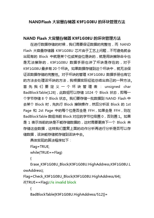
NANDFlash大容量存储器K9F1G08U的坏块管理方法NAND Flash大容量存储器K9F1G08U的坏块管理方法在进行数据存储的时候,我们需要保证数据的完整性,而NAND Flash大容量存储器K9F1G08U芯片由于工艺上问题,不可避免就会出现有的Block中就是某个位或某些位是块的,就是用块擦除命令也是无法擦除的,K9F1G08U数据手册也讲了坏块是存在的,对于K9F1G08U最多有20个坏块。
如果数据存储到这个坏块中,就无法保证该数据存储的完整性。
对于坏块的管理K9F1G08U数据手册也有它的方法去处理该坏块的方法,我根据实际经验总结出自己的一种方法。
首先我们要定义一个坏块管理表:unsigned char BadBlockTable[128],此数组可以存储1024个Block状态,即每一个字节存储8个Block状态。
我们要存储一批数据到NAND Flash中去某个Block时,先执行Block擦除操作,然后分析该Block的1st Page和2st Page中的每个位是否全是FFH,如果全是FFH,则在BadBlockTable数组当前Block对应的字节位给置0,否则置1。
如果是1表示当前的块是不能存储数据的,这时需要更换下一个Block来存储这些数据,这样我们重复上面的动作分析再进行分析是否可以存储数据,该块能存储就存储到该块中去。
具体实现的算法程序如下:Flag=TRUE;while(TRUE==Flag){Erase_K9F1G08U_Block(K9F1G08U.HighAddress,K9F1G08U.L owAddress);Flag=Check_K9F1G08U_Block(K9F1G08U.HighAddress/64);if(TRUE==Flag)//is invalid block{BadBlockTable[K9F1G08U.HighAddress/512]|=(1<<(K9F1G08U.HighAddress%8));K9F1G08U.HighAddress+=64;//Point to Next Block}else// is valid block ,record to BadBlockTable{BadBlockTable[K9F1G08U.HighAddress/512]&=~(1<<(K9F1G08U.HighAddress%8));}}for(i=0;i<sizeof(BadBlockTable);i++)Write_RAM(RAM_BANK_0,K9F1G08U_BAD_BLOCK+i,BadBlo ckTable[i]);。
(完整版)单板硬件测试规范

页数:第1 页共74 页电源单板硬件测试规范修订信息登记表目录前言 (5)摘要: (5)关键词: (5)缩略词解释 (5)一.目的 (5)二.适用范围 (5)三.引用/参考标准或资料 (5)四.名词解释 (5)五.测试基本原则及判定准则 (5)5.1 测试基本原则 (5)5.2 技术指标说明 (6)5.3 不合格测试项目分类准则 (6)5.4 质量判定准则 (6)5.5 测试准备 (6)六.测试仪器、测试工具、测试环境 (6)6.1 测试仪器 (7)6.2 测试工具 (7)6.3 测试环境 (7)七.测试项目、测试说明、测试方法、判定标准 (7)7.1 外观及尺寸审查 (7)7.2 电路原理图审查 (8)7.2.1 基准电路 (8)7.2.2 滤波电路 (8)7.2.3 保护电路 (10)7.2.4 看门狗电路 (10)7.2.5 ID电路 (12)7.2.6 缓冲驱动电路 (12)7.2.7 锁存电路 (13)7.2.8 分压电路 (14)7.2.9 键盘电路 (14)7.2.10模拟量通道选择电路 (15)7.2.11 有效值电路 (17)7.2.12 差分放大电路 (18)7.2.13 压频转换电路 (19)7.2.14 RS485/422电路 (21)7.2.15 RS232电路 (26)7.2.16 CAN电路 (27)7.2.17 CPU基本电路审查 (29)7.2.17.1 MCS51基本电路 (29)7.2.17.2 TI DSP基本电路 (30)7.2.17.3 MPC852基本电路 (33)7.2.17.4 ARM基本电路 (34)7.2.18 继电器电路 (37)7.2.19 交流电压采样电路 (39)7.3 信号测量 (40)7.3.1 基准电路 (40)7.3.2 看门狗电路 (42)7.3.3 时钟电路 (43)7.3.4 ID电路 (44)7.3.5 分压电路 (45)7.3.6 IIC电路 (46)7.3.7 有效值电路 (47)7.3.8 平均值电路 (47)7.3.9 差分放大电路 (49)7.3.10 交流频率采样电路 (49)7.3.11 电池熔丝状态检测电路 (51)7.3.12 压频转换电路 (53)7.3.13 光耦固态继电器 (54)7.3.14 光藕电路 (55)7.3.15 RS485/422电路 (55)7.3.16 RS232电路 (56)7.3.17 CAN电路 (57)7.3.18 CPU电路信号测量 (59)7.3.18.1 MCS51单片机基本电路 (59)7.3.18.2 DSP基本电路 (59)7.3.18.3 MPC852基本电路 (61)7.3.18.4 ARM基本电路 (62)7.4 电路计算 (63)7.4.1 TVS电路 (63)7.4.2 光耦固态继电器 (65)7.4.3 光藕计算 (66)7.4.4 差分放大电路计算 (69)7.4.5 单板电路功耗计算 (69)7.5 研究性测试 (70)7.5.1 近场骚扰测试 (70)八.附录 (73)8.1 测试方案模板 (73)8.2 测试项目手册模板 (73)8.3 单板测试CheckList (73)8.4 整流模块DSP硬件测试规范 (73)8.5 逻辑电平 (74)前言摘要:本规范介绍了电源单板硬件测试的项目、测试方法以及测试原理。
单板硬件测试规范

电源单板硬件测试规范修订信息登记表目录前言.................................................. 错误!未定义书签。
摘要:................................................ 错误!未定义书签。
关键词:................................................ 错误!未定义书签。
缩略词解释.............................................. 错误!未定义书签。
一.目的......................................... 错误!未定义书签。
二.适用范围......................................... 错误!未定义书签。
三.引用/参考标准或资料.............................. 错误!未定义书签。
四.名词解释......................................... 错误!未定义书签。
五.测试基本原则及判定准则........................... 错误!未定义书签。
测试基本原则 .......................................... 错误!未定义书签。
技术指标说明 .......................................... 错误!未定义书签。
不合格测试项目分类准则 ................................ 错误!未定义书签。
质量判定准则 .......................................... 错误!未定义书签。
测试准备 .............................................. 错误!未定义书签。
K9LAG08U0M芯片手册读后感(huyunqing)
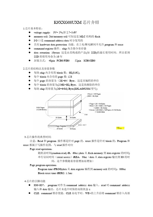
K9XXG08UXM芯片介绍1.芯片基本特征:z voltage supply: 3V+-5%,即2.7~3.6Vz memory cell: 2bit/memory cell可知这是MLC结构的flashz I/O口是command address data时分复用的z具有hardware data protection 功能,在上电/断电瞬间不允许program和erasez command register操作,chip内含指令寄存器z data retention: 10years 这是由其构成的产品(如SSD)的最长使用时间,所以看到SSD的使用寿命为10年z封装方式: 48pin--PCB0/PIB0 52pin—ICB0/IIB02.芯片的结构以及容量参数z每块chip内含有的block数:8K(8192),z每个block内含有的page数: 128z每个page的容量为(2K+64)Byte,这是页编程的单位z每个block的容量为(256K+8K) Byte,这是块擦除的单位z每块chip的容量为(2G+64M) Byte(K9LAG0U0M型号)3.芯片操作的典型时间:注意:Read和program 操作都是针对page的,erase操作是针对block的;Program和erase都属于写操作范围,与read操作对应Page read operation:随机读时间(random read) tR:60us (data从flash memory到data register的时间)串行访问时间(serial access)tREA:30ns(data从data register输出到IO的时间,这个参数随着容量增加而增加)Page program operation:Program time tPROG(data从data register编程到memory cell的时间):800usBlock erase time tBERS: 1.5ms4.芯片的引脚功能z IO0~IO7: program时作为command address data输入,read时command address 输入和data输出,芯片未选中时保持高阻状态zz CLE: command锁存使能,CLE高电平时,WE~的上升沿将command锁存入内部command registerz ALE:address锁存使能,ALE高电平时,WE~的上升沿将address锁存入内部address register,因address长度的不同所需地址周期也不同z RE~:使得在data register中的data输出,RE下降沿tREA时间后输出有效(这是serial access time),并将自动增加内部page的column地址计数器(能够连续读取data)z WE~:WE上升沿时可以写入command address dataz WP~:写保护端,在上电/断电瞬间有效,有效时将禁止program/erase操作z R/B~:高时表明flash芯片准备好待操作,低时表明正在进行program/erase/ random read 操作;random read operation是data从memory cell到data register的这段操作,random write是data从data register到memory cell这一段操作;当data在memory cell和data register之间交换时(包括随机读和随机写)RB~出现低电平表z Vcc:powerz Vss:groundz NC:not connect5. 芯片操作时的寻址周期:z A0~A11: column address 访问范围2K(一个page)z A12~A31: row address 访问chip中的8K个block 及block中的128个page地址(13+7)z每个cycle传送8位address, column address和row address不能在同一个cycle里传送,不足的address位接低电平0z可知传送一个完整地址需要2个column寻址周期+3个row寻址周期,一共5个周期z Block erase只需要3个rom 寻址周期(为何不是2个?)z每个page的Spare 64Byte 的访问是column address的最后64(2048~2111)6. 指令执行所需周期数Block erase, page program, page read等指令需要2周期(但并不连续,一般是在第一个命令周期内发送寻址命令,第二个命令周期内发送数据传送命令)reset, status read等指令只需要一个周期7. flash芯片操作指令一览8.read flow、program flow、erase flow注意program flow, erase flow依靠R/B~ 和IO0来判断过程是否完成,read flow通过校验ECC来判断过程是否完成14.关于芯片的坏块z Flash芯片出厂时可能含有少量坏块(invalid block)z坏块数量会随使用时间的增加而增加z一个坏块不会影响其他好块,这与结构有关z三星公司保证每块flash芯片的第一个block是好块z三星公司保证坏块的最后一个page中没有FFh数据(address:2048),这也是检测坏块的方法(在K9WBG08U0M芯片中块定义不同)15.flash芯片的interleave 操作Interleave操作允许同时操作一个chip中的两个die,以interleave page program为例:阶段A:die1进入编程阶段,R/B~1显示忙,此时可以继续向die2发送命令阶段B:die1和die2都进入编程阶段,R/B~1和R/B~2都显示忙阶段C:die1已经完成编程,die2仍在编程中阶段D:die1和die2都完成编程,R/B~显示空闲,可以再次进行interleave操作HYQ2009-3-27。
单板测试
测试规范(单板)
共同测试项目:
MPU、DTV、FAX、ISDN、AT0、ASL、PWR都要386能运行,以太网可以下载,可以正常开工,按测试流程实行高温运行试验、低温贮存试验、振动试验。
一、MPU板
可以正常运行,能够下载,需要测试每个HW的放音收号(两个机框、级联),七号386运行、下载,能够跑七号配置的链路;各个指示灯正常。
二、DTV板
主386和8031能够运行,以太网能下载,DTMF(收号)MFC (呼叫)录放音,有会议芯片要具有会议功能,收号要准,放音无磕碰,杂音或失真的声音;各指示灯要闪烁正常。
三、FAX板
主386和8031能够运行,以太网能下载,各个工作指示灯要闪烁正常,传真板的每一路传真要具有收发功能(无缺页,图文清晰)。
四、ISDN板
主386和8031能够运行,以太网能下载,测试时需要把ISDN下载Newmon.bin,然后运行XHM386.exe,导入ISDN.abs文件,给予200410a和200c10a两个地址,进行收发数据测试,测试完后下载回ISDN.bin进行ping命令测试就可以了。
五、AT0板
8031能够运行,各个指示灯正常,每一个通道能够拨出、拨入,放音、收号正常。
六、ASL板
8031能够运行,各个指示灯正常,每一个通道摘挂机、放音、收号、振铃正常。
七、PWR板
+5V、-5V、铃流75V电压正常,需要带上负载进行老化测试(老化4小时)。
八、机箱
各槽位配相应板能正常开工,同轴线接口良好,以太网接口良好。
九、一次电源
带上负载老化,在老化的过程中各指示灯和仪表均显示正常(老化48小时)。
测试流程图。
科力达K9产品手册范本精选全文完整版

可编辑修改精选全文完整版科力达RTK 产品系列风云K9系列RTK测量系统产品手册科力达仪器二○一五年四月目录第一章风云K9系列RTK概述 (3)§1.1关于风云K9 (3)§1.2二大独创 (3)§1.3四大特色 (4)§1.4技术特色 (4)第二章风云K9系列RTK主机 (6)§2.1主机外型 (6)§2.2接口 (7)§2.3电池的安装方法 (7)§2.4指示灯和仪器设置 (8)§2.5手簿与蓝牙连接 (13)§2.5.1 手簿设置 (13)§2.5.2 连接设置 (17)§2.6网络设置连接 (18)第三章风云K9系列RTK电台 (23)§3.1电台概述 (23)§3.1.1 产品简介 (23)§3.1.2 产品特点 (23)§3.1.3 技术指标 (24)§3.2GDL25电台外型说明 (25)§3.2.1 GDL25电台的面板 (25)§3.2.2 GDL25电台的外型 (26)§3.3GDL25电台使用注意事项 (26)§3.3.1 供电电源 (26)§3.3.2 天线口负载 (27)§3.3.3 电磁环境 (27)§3.3.4 天线选择 (28)§3.3.5 接口电缆 (28)第四章风云K9系列RTK附件介绍 (29)§4.1风云K9系列GPS的仪器箱(包) (29)§4.2电池及充电器 (29)§4.3数据收天线及发射天线 (31)§4.4各种传输线及电缆 (32)§4.5其他 (33)第五章操作说明 (34)§5.1基准站和移动站安装 (34)§5.2仪器设置 (35)§5.3仪器操作表现 (35)§5.4天线高的量测方法 (35)第六章与软件的连接 (37)§6.1数据传输 (37)§6.1.1 磁盘拷贝 (37)§6.1.2 仪器之星的使用 (37)§6.2在线升级方法 (39)§6.3K9系列GPS的注册 (41)附录1 技术参数 (43)附录2 联系方式 (44)第一章风云K9系列RTK概述§1.1 关于风云K9科力达仪器一直致力于把国际先进的GPS测绘勘测技术与产品普及到国测量用户手中。
单板硬件测试项目测试说明测试方法判定标准

单板硬件测试项目测试说明测试方法判定标准7.1 外观及尺寸审查● 测试说明:1) 初样样机单板飞线不能超过3处,不能存在飞器件;其他版本样机不能存在飞线和飞器件现象;2) 插座应该有防插错功能;(详见保护电路测试)3) 建议有电源指示灯或电源指示灯接口4)样机尺寸应符合规格书要求● 测试方法:外观:目测。
尺寸:使用长度量具测量。
● 判定标准:符合测试说明,合格;否则,则判定不合格。
● 参考案例:案例1【现象描述】SM模块的电源输入口与RS485通讯口的插座相同,无防插座处理,导致测试时,将RS485通讯线与电源输入口差错,从而将连接在RS485总线的所有SM 模块端口损坏。
7.2 电路原理图审查7.2.1 基准电路测试说明:模拟量在采样时需要有基准电路,当基准发生变化时,将导致模拟量采样发生漂移或严重偏离实际输入。
电压基准源分为并联型和串联稳压型。
并联型基准主要是利用半导体结的正负温度特性,通过设计一定的间隙电压下,其温度系数最小。
一般的间隙电压有 2.5V,1.24V,1.225V等。
2.5V我司主要推荐使用AZ431,HA17431H。
1.24V 主要使用AZ431L,LMV431。
1.225V 主要采用LM4041,TS4041。
串联稳压型,其结构同电压调整器类似,其内部一般也需要一个基准源,外部有高精度的反馈网络。
由于一般要采用特殊的工艺,制程较复杂,价格较贵。
此基准能做到高精度,低温度系数。
主要用于高精度和低温漂的场合。
串联型基准主要采用2.5V,2.048V基准。
SOT-23封装是以后主要封装,3~5年内基本不会淘汰。
我司推荐ADR380,MAX6021 。
基准电路的基准源的选取应该使用公司推荐的芯片。
同时基准只用于电压参考,不允许直接用于作电源供电或输出较大的电流。
● 测试方法:1. 基准电路的基准源的选取应该满足测试说明,否则提一建议问题。
2. 检查电路原理图,基准是否只用于电压参考,不允许直接用于作电源供电或输出较大的电流。
K9K2G08U0M-V中文资料
Document Title256M x 8 Bit / 128M x 16 Bit NAND Flash Memory Revision HistoryThe attached data sheets are prepared and approved by SAMSUNG Electronics. SAMSUNG Electronics CO., LTD. reserve the rightto change the specifications. SAMSUNG Electronics will evaluate and reply to your requests and questions about device. If you have any questions, please contact the SAMSUNG branch office near your office.Revision No0.00.10.20.30.40.50.60.70.8RemarkAdvanceHistory1. Initial issue1. I OL (R/B) of 1.8V device is changed.-min. Value: 7mA -->3mA -typ. Value: 8mA -->4mA1. 5th cycle of ID is changed : 40h --> 44h1. Add WSOP Package Dimensions.1. Add two-K9K2GXXU0M-YCB0/YIB0 Stacked Package 1. Min valid block of K9W4GXXU1M-YCB0/YIB0 is changed .- min. 4016 --> 40361. Each K9K2GXXX0M chip in the K9W4GXXU1M has Maximum 30invalid blocks.2. K9W4GXXU1M’s ID is changed (Before)(After)1. Add the Rp vs tr ,tf & Rp vs ibusy graph for 1.8V device (Page 36)2. Add the data protection Vcc guidence for 1.8V device - below about 1.1V. (Page 37)The min. Vcc value 1.8V devices is changed.K9K2GXXQ0M : Vcc 1.65V~1.95V --> 1.70V~1.95VDevice 2nd Cycle 3rd cycle 4th Cycle 5th Cycle K9W4G08U1M DCh C315h 4Ch K9W4G16U1M CChC355h4ChDevice 2nd Cycle 3rd cycle 4th Cycle 5th Cycle K9W4G08U1M DAh C115h 44h K9W4G16U1MCAhC155h44hDraft DateAug. 30.2001Nov. 5.2001Jan. 23. 2002May.29.2002Aug.13.2002Aug. 22.2002Nov. 07.2002Nov. 22.2002Mar. 6.2003Document Title256M x 8 Bit / 128M x 16 Bit NAND Flash MemoryRevision HistoryThe attached data sheets are prepared and approved by SAMSUNG Electronics. SAMSUNG Electronics CO., LTD. reserve the rightto change the specifications. SAMSUNG Electronics will evaluate and reply to your requests and questions about device. If you have any questions, please contact the SAMSUNG branch office near your office.Revision No0.91.01.11.21.31.4RemarkHistoryPb-free Package is added.K9K2G08U0M-FCB0,FIB0K9K2G08Q0M-PCB0,PIB0K9K2G08U0M-PCB0,PIB0K9K2G16U0M-PCB0,PIB0K9K2G16Q0M-PCB0,PIB0K9W4G08U1M-PCB0,PIB0,ECB0,EIB0K9W4G16U1M-PCB0,PIB0,ECB0,EIB0Errata is added.(Front Page)-K9K2GXXQ0MtWC tWP tWH tRC tREH tRP tREA tCEA Specification 45 25 15 50 15 25 30 45Relaxed value 80 60 20 80 20 60 60 751. The 3rd Byte ID after 90h ID read command is don’t cared. The 5th Byte ID after 90h ID read command is deleted.New package dimension is added.(K9W4GXXU1M-KXB0/EXB0)1. Min valid block of K9W4GXXU1M-YCB0/YIB0 is changed .- min. 4036 --> 40162. Note is added.(VIL can undershoot to -0.4V and VIH can overshoot to VCC +0.4V for durations of 20 ns or less.)AC parameters are changed-K9K2GXXQ0MtWC tWP tWH tRC tREH tRP tREA tCEA Before 45 25 15 50 15 25 30 45After 80 60 20 80 20 60 60 75Draft DateMar. 13.2003Mar. 17.2003Apr. 9. 2003Apr. 15. 2003Apr. 18. 2003Aug. 5. 2003GENERAL DESCRIPTIONFEATURES• Voltage Supply-1.8V device(K9K2GXXQ0M): 1.7V~1.95V -3.3V device(K9XXGXXUXM): 2.7 V ~3.6 V • Organization- Memory Cell Array-X8 device(K9K2G08X0M) : (256M + 8,192K)bit x 8bit -X16 device(K9K2G16X0M) : (128M + 4,096K)bit x 16bit - Data Register-X8 device(K9K2G08X0M): (2K + 64)bit x8bit -X16 device(K9K2G16X0M): (1K + 32)bit x16bit - Cache Register-X8 device(K9K2G08X0M): (2K + 64)bit x8bit -X16 device(K9K2G16X0M): (1K + 32)bit x16bit • Automatic Program and Erase - Page Program-X8 device(K9K2G08X0M): (2K + 64)Byte -X16 device(K9K2G16X0M): (1K + 32)Word - Block Erase-X8 device(K9K2G08X0M): (128K + 4K)Byte -X16 device(K9K2G16X0M): (64K + 2K)Word • Page Read Operation - Page Size- X8 device(K9K2G08X0M): 2K-Byte - X16 device(K9K2G16X0M) : 1K-Word - Random Read : 25µs(Max.) - Serial Access1.8V device(K9K2GXXQ0M): 80ns(Min.) 3.3V device(K9XXGXXUXM): 50ns(Min.)256M x 8 Bit / 128M x 16 Bit NAND Flash Memory• Fast Write Cycle Time- Program time : 300µs(Typ.) - Block Erase Time : 2ms(Typ.)• Command/Address/Data Multiplexed I/O Port • Hardware Data Protection- Program/Erase Lockout During Power Transitions • Reliable CMOS Floating-Gate Technology - Endurance : 100K Program/Erase Cycles - Data Retention : 10 Years • Command Register Operation• Cache Program Operation for High Performance Program • Power-On Auto-Read Operation • Intelligent Copy-Back Operation • Unique ID for Copyright Protection • Package :- K9K2GXXX0M-YCB0/YIB048 - Pin TSOP I (12 x 20 / 0.5 mm pitch) - K9K2G08U0M-VCB0/VIB048 - Pin WSOP I (12X17X0.7mm) - K9K2GXXX0M-PCB0/PIB048 - Pin TSOP I (12 x 20 / 0.5 mm pitch)- Pb-free Package - K9K2G08U0M-FCB0/FIB048 - Pin WSOP I (12X17X0.7mm)- Pb-free Package * K9K2G08U0M-V,F(WSOPI ) is the same device as K9K2G08U0M-Y ,P(TSOP1) except package type.- K9W4GXXU1M-YCB0,PCB0/YIB0,PIB0 : Two K9K2G08U0M stacked.48 - Pin TSOP I (12 x 20 / 0.5 mm pitch)- K9W4GXXU1M-KCB0,ECB0/KIB0,EIB0 : Two K9K2G08U0M stacked.48 - Pin TSOP I (12 x 17 / 0.5 mm pitch)Offered in 256Mx8bit or 128Mx16bit, the K9K2GXXX0M is 2G bit with spare 64M bit capacity. Its NAND cell provides the most cost-effective solution for the solid state mass storage market. A program operation can be performed in typical 300µs on the 2112-byte(X8device) or 1056-word(X16 device) page and an erase operation can be performed in typical 2ms on a 128K-byte(X8 device) or 64K-word(X16 device) block. Data in the data page can be read out at 80ns(1.8V device) or 50ns(3.3V device) cycle time per byte(X8device) or word(X16 device). The I/O pins serve as the ports for address and data input/output as well as command input. The on-chip write controller automates all program and erase functions including pulse repetition, where required, and internal verification and margining of data. Even the write-intensive systems can take advantage of the K9K2GXXX0M ′s extended reliability of 100K program/erase cycles by providing ECC(Error Correcting Code) with real time mapping-out algorithm. The K9K2GXXX0M is an optimum solu-tion for large nonvolatile storage applications such as solid state file storage and other portable applications requiring non-volatility.An ultra high density solution having two 2Gb stacked with two chip selects is also available in standard TSOPI package.PRODUCT LISTPart Number Vcc Range OrganizationPKG TypeK9K2G08Q0M-Y ,P 1.7 ~ 1.95VX8TSOP1K9K2G16Q0M-Y ,P X16K9XXG08UXM-Y ,P ,K,E 2.7 ~ 3.6V X8K9XXG16UXM-Y ,P ,K,E X16K9K2G08U0M-V,FX8WSOP1PIN CONFIGURATION (TSOP1)K9K2GXXX0M-YCB0,PCB0/YIB0,PIB0X8X16X16X8PACKAGE DIMENSIONS48-PIN LEAD/LEAD FREE PLASTIC THIN SMALL OUT-LINE PACKAGE TYPE(I)48 - TSOP1 - 1220FUnit :mm/Inch0.787±0.00820.00±0.20#1#240.20+0.07-0.030.008+0.003-0.0010.500.0197#48#250.48812.40M A X12.000.4720.10 0.004M A X 0.250.010()0.039±0.0021.00±0.050.0020.05MIN0.0471.20MAX0.45~0.750.018~0.0300.724±0.00418.40±0.100~8°0.0100.25T Y P0.125+0.0750.0350.005+0.003-0.0010.500.020()48-pin TSOP1Standard Type 12mm x 20mm123456789101112131415161718192021222324484746454443424140393837363534333231302928272625N.C N.C N.C N.C N.C N.C R/B RE CE N.C N.C Vcc Vss N.C N.C CLE ALE WE WP N.C N.C N.C N.C N.CN.C N.C N.C N.C I/O7I/O6I/O5I/O4N.C N.C PRE Vcc Vss N.C N.C N.C I/O3I/O2I/O1I/O0N.C N.C N.C N.CN.C N.C N.C N.C N.C N.C R/B RE CE N.C N.C Vcc Vss N.C N.C CLE ALE WE WP N.C N.C N.C N.C N.CVss I/O15I/O7I/O14I/O6I/O13I/O5I/O12I/O4N.C PRE Vcc N.C N.C N.C I/O11I/O3I/O10I/O2I/O9I/O1I/O8I/O0VssPIN CONFIGURATION (WSOP1)K9K2G08U0M-VCB0,FCB0/VIB0,FIB0PACKAGE DIMENSIONS48-PIN LEAD/LEAD FREE PLASTIC VERY VERY THIN SMALL OUT-LINE PACKAGE TYPE (I)48 - WSOP1 - 1217FUnit :mm15.40±0.10#1#240.20+0.07-0.030.16+0.07-0.030.50T Y P (0.50±0.06)#48#2512.00±0.100.10+0.075-0.0350.58±0.040.70 MAX(0.1Min)17.00±0.200°~8°0.45~0.75123456789101112131415161718192021222324484746454443424140393837363534333231302928272625N.C N.C DNU N.C N.C N.C R/B RE CE DNU N.C Vcc Vss N.C DNU CLE ALE WE WP N.C N.C DNU N.C N.CN.C N.C DNU N.C I/O7I/O6I/O5I/O4N.C DNU N.C Vcc Vss N.C DNU N.C I/O3I/O2I/O1I/O0N.C DNU N.C N.CPIN CONFIGURATION (TSOP1)K9W4G08U1M-YCB0,PCB0/YIB0,PIB0PACKAGE DIMENSIONS48-PIN LEAD/LEAD FREE PLASTIC THIN SMALL OUT-LINE PACKAGE TYPE(I)48 - TSOP1 - 1220FUnit :mm/Inch0.787±0.00820.00±0.20#1#240.16+0.07-0.030.008+0.003-0.0010.500.0197#48#250.48812.40M A X12.000.4720.10 0.004M A X 0.250.010()0.039±0.0021.05±0.030.0020.02MIN0.0471.20MAX0.45~0.750.018~0.0300.724±0.00418.40±0.100~8°0.0100.25T Y P0.125+0.0750.0350.005+0.003-0.0010.500.020()48-pin TSOP1Standard Type 12mm x 20mm123456789101112131415161718192021222324484746454443424140393837363534333231302928272625N.C N.C N.C N.C N.C R/B2R/B1 RE CE1CE2N.C Vcc Vss N.C N.C CLE ALE WE WP N.C N.C N.C N.C N.CN.C N.C N.C N.C I/O7I/O6I/O5I/O4N.C N.C PRE Vcc Vss N.C N.C N.C I/O3I/O2I/O1I/O0N.C N.C N.C N.CX16N.C N.C N.C N.C N.C R/B2R/B1 RE CE1CE2N.C Vcc Vss N.C N.C CLE ALE WE WP N.C N.C N.C N.C N.CX16Vss I/O15I/O7I/O14I/O6I/O13I/O5I/O12I/O4N.C PRE Vcc N.C N.C N.C I/O11I/O3I/O10I/O2I/O9I/O1I/O8I/O0VssX8X8PIN CONFIGURATION (TSOP1)PACKAGE DIMENSIONS48-PIN LEAD/LEAD FREE PLASTIC THIN SMALL OUT-LINE PACKAGE TYPE (I)48 - TSOP1 - 1217FUnit :mm15.40±0.10#1#240.20+0.07-0.030.16+0.07-0.030.50T Y P (0.50±0.06)#48#2512.00±0.100.15+0.075-0.0351.00±0.031.15 MAX(0.02Min)17.00±0.200°~8°0.45~0.75123456789101112131415161718192021222324484746454443424140393837363534333231302928272625N.C N.C N.C N.C N.C R/B2R/B1 RE CE1CE2N.C Vcc Vss N.C N.C CLE ALE WE WP N.C N.C N.C N.C N.CN.C N.C N.C N.C I/O7I/O6I/O5I/O4N.C N.C PRE Vcc Vss N.C N.C N.C I/O3I/O2I/O1I/O0N.C N.C N.C N.CX16N.C N.C N.C N.C N.C R/B2R/B1 RE CE1CE2N.C Vcc Vss N.C N.C CLE ALE WE WP N.C N.C N.C N.C N.CX16Vss I/O15I/O7I/O14I/O6I/O13I/O5I/O12I/O4N.C PRE Vcc N.C N.C N.C I/O11I/O3I/O10I/O2I/O9I/O1I/O8I/O0VssX8X8K9W4G08U1M-KCB0,ECB0/KIB0,EIB048-pin TSOP112mm x 17mmPIN DESCRIPTIONNOTE : Connect all V CC and V SS pins of each device to common power supply outputs. Do not leave V CC or V SS disconnected.Pin Name Pin FunctionI/O 0 ~ I/O 7(K9K2G08X0M)I/O 0 ~ I/O 15(K9K2G16X0M)DATA INPUTS/OUTPUTSThe I/O pins are used to input command, address and data, and to output data during read operations. The I/O pins float to high-z when the chip is deselected or when the outputs are disabled.I/O8 ~ I/O15 are used only in X16 organization device. Since command input and address input are x8 oper-ation, I/O8 ~ I/O15 are not used to input command & address. I/O8 ~ I/O15 are used only for data input and output.CLECOMMAND LATCH ENABLEThe CLE input controls the activating path for commands sent to the command register. When active high, commands are latched into the command register through the I/O ports on the rising edge of the WE signal.ALEADDRESS LATCH ENABLEThe ALE input controls the activating path for address to the internal address registers. Addresses are latched on the rising edge of WE with ALE high.CE / CE1CHIP ENABLEThe CE / CE1 input is the device selection control. When the device is in the Busy state, CE / CE1 high is ignored, and the device does not return to standby mode in program or erase opertion. Regarding CE / CE1 control during read operation, refer to ’Page read’ section of Device operation .CE2CHIP ENABLEThe CE2 input enables the second K9K2GXXU0MREREAD ENABLEThe RE input is the serial data-out control, and when active drives the data onto the I/O bus. Data is valid tREA after the falling edge of RE which also increments the internal column address counter by one.WEWRITE ENABLEThe WE input controls writes to the I/O port. Commands, address and data are latched on the rising edge of the WE pulse.WPWRITE PROTECTThe WP pin provides inadvertent write/erase protection during power transitions. The internal high voltage generator is reset when the WP pin is active low.R/B / R/B1READY/BUSY OUTPUTThe R/B / R/B1 output indicates the status of the device operation. When low, it indicates that a program, erase or random read operation is in process and returns to high state upon completion. It is an open drain output and does not float to high-z condition when the chip is deselected or when outputs are disabled.R/B2READY/BUSY OUTPUTThe R/B2 output indicates the status of the second K9K2GXXU0MPREPOWER-ON READ ENABLEThe PRE controls auto read operation executed during power-on. The power-on auto-read is enabled when PRE pin is tied to Vcc.Vcc POWERV CC is the power supply for device. Vss GROUNDN.CNO CONNECTIONLead is not internally connected.Product IntroductionThe K9K2GXXX0M is a 2112Mbit(2,214,592,512 bit) memory organized as 131,072 rows(pages) by 2112x8(X8 device) or 1056x16(X16 device) columns. Spare 64(X8) or 32(X16) columns are located from column address of 2048~2111(X8 device) or 1024~1055(X16 device). A 2112-byte(X8 device) or 1056-word(X16 device) data register and a 2112-byte(X8 device) or 1056-word(X16 device) cache register are serially connected to each other. Those serially connected registers are connected to memory cell arrays for accommodating data transfer between the I/O buffers and memory cells during page read and page program opera-tions. The memory array is made up of 32 cells that are serially connected to form a NAND structure. Each of the 32 cells resides in a different page. A block consists of two NAND structured strings. A NAND structure consists of 32 cells. Total 1081344 NAND cells reside in a block. The program and read operations are executed on a page basis, while the erase operation is executed on a block basis. The memory array consists of 2048 separately erasable 128K-byte(X8 device) or 64K-word(X16 device) blocks. It indicates that the bit by bit erase operation is prohibited on the K9K2GXXX0M.The K9K2GXXX0M has addresses multiplexed into 8 I/Os(X16 device case : lower 8 I/Os). This scheme dramatically reduces pin counts and allows system upgrades to future densities by maintaining consistency in system board design. Command, address and data are all written through I/O's by bringing WE to low while CE is low. Those are latched on the rising edge of WE. Command Latch Enable(CLE) and Address Latch Enable(ALE) are used to multiplex command and address respectively, via the I/O pins. Some com-mands require one bus cycle. For example, Reset Command, Status Read Command, etc require just one cycle bus. Some other commands, like page read and block erase and page program, require two cycles: one cycle for setup and the other cycle for execu-tion. The 256M byte(X8 device) or 128M word(X16 device) physical space requires 29(X8) or 28(X16) addresses, thereby requiring four cycles for addressing: 2 cycles of column address, 3 cycles of row address, in that order. Page Read and Page Program need the same four address cycles following the required command input. In Block Erase operation, however, only the two row address cycles are used. Device operations are selected by writing specific commands into the command register. Table 1 defines the specific commands of the K9K2GXXX0M.The device provides cache program in a block. It is possible to write data into the cache registers while data stored in data registers are being programmed into memory cells in cache program mode. The program performace may be dramatically improved by cache program when there are lots of pages of data to be programmed.The device embodies power-on auto-read feature which enables serial access of data of the 1st page without command and address input after power-on.In addition to the enhanced architecture and interface, the device incorporates copy-back program feature from one page to another page without need for transporting the data to and from the external buffer memory. Since the time-consuming serial access and data-input cycles are removed, system performance for solid-state disk application is significantly increased.Table 1. Command SetsFunction1st. Cycle2nd. Cycle Acceptable Command during Busy Read 00h30hRead for Copy Back00h35hRead ID90h-Reset FFh-OPage Program80h10hCache Program80h15hCopy-Back Program85h10hBlock Erase60h D0hRandom Data Input*85h-Random Data Output*05h E0hRead Status70h ONOTE : 1. Random Data Input/Output can be executed in a page.Caution : Any undefined command inputs are prohibited except for above command set of Table 1.DC AND OPERATING CHARACTERISTICS (Recommended operating conditions otherwise noted.)NOTE : V IL can undershoot to -0.4V and V IH can overshoot to V CC +0.4V for durations of 20 ns or less.ParameterSymbol Test Conditions K9K2GXXQ0M(1.8V)K9XXGXXUXM(3.3V)UnitMin Typ Max Min Typ Max Operat-ingCurrent Page Read withSerial AccessI CC 1tRC=50ns, CE=V IL I OUT =0mA-1020-1530mA ProgramI CC 2--1020-1530EraseI CC 3--1020-1530Stand-by Current(TTL)I SB 1CE=V IH , WP=PRE=0V/V CC--1--1Stand-by Current(CMOS)I SB 2CE=V CC -0.2, WP=PRE=0V/V CC -20100-20100µA Input Leakage Current I LI V IN =0 to Vcc(max)--±20--±20Output Leakage Current I LO V OUT =0 to Vcc(max)--±20--±20Input High VoltageV IH*-V CC -0.4-V CC +0.3 2.0-V CC +0.3V Input Low Voltage, All inputs V IL*--0.3-0.4-0.3-0.8Output High Voltage Level V OH K9K2GXXQ0M:I OH =-100µA K9XXGXXUXM:I OH =-400µA Vcc-0.1-- 2.4--Output Low Voltage LevelV OL K9K2GXXQ0M :I OL =100uA K9XXGXXUXM :I OL =2.1mA --0.1--0.4Output Low Current(R/B)I OL (R/B)K9K2GXXQ0M :V OL =0.1V K9XXGXXUXM :V OL =0.4V34-810-mA RECOMMENDED OPERATING CONDITIONS(Voltage reference to GND, K9XXGXXXXM-XCB0 :T A =0 to 70°C, K9XXGXXXXM-XIB0:T A =-40 to 85°C)Parameter Symbol K9K2GXXQ0M(1.8V)K9XXGXXUXM(3.3V)Unit Min Typ.Max Min Typ.Max Supply Voltage V CC 1.7 1.8 1.95 2.7 3.3 3.6V Supply VoltageV SSVABSOLUTE MAXIMUM RATINGSNOTE :1. Minimum DC voltage is -0.6V on input/output pins. During transitions, this level may undershoot to -2.0V for periods <30ns. Maximum DC voltage on input/output pins is V CC,+0.3V which, during transitions, may overshoot to V CC +2.0V for periods <20ns.2. Permanent device damage may occur if ABSOLUTE MAXIMUM RATINGS are exceeded. Functional operation should be restricted to the conditions as detailed in the operational sections of this data sheet. Exposure to absolute maximum rating conditions for extended periods may affect reliability.ParameterSymbol RatingUnit K9K2GXXQ0M(1.8V) K9XXGXXUXM(3.3V)Voltage on any pin relative to V SS V IN/OUT -0.6 to + 2.45-0.6 to + 4.6V V CC -0.2 to + 2.45-0.6 to + 4.6Temperature Under Bias K9XXGXXXXM-XCB0T BIAS -10 to +125°C K9XXGXXXXM-XIB0-40 to +125Storage Temperature K9XXGXXXXM-XCB0T STG -65 to +150°C K9XXGXXXXM-XIB0Short Circuit CurrentIos5mACAPACITANCE (T A =25°C, V CC =1.8V/3.3V, f=1.0MHz)NOTE : Capacitance is periodically sampled and not 100% tested.ItemSymbol Test ConditionMaxUnit K9K2GXXX0MK9W4GXXU1MInput/Output Capacitance C I/O V IL =0V 2040pF Input CapacitanceC INV IN =0V2040pFVALID BLOCKNOTE :1. The device may include invalid blocks when first shipped. Additional invalid blocks may develop while being used. The number of valid blocks is pre-sented with both cases of invalid blocks considered. Invalid blocks are defined as blocks that contain one or more bad bits . Do not erase or pro-gram factory-marked bad blocks. Refer to the attached technical notes for appropriate management of invalid blocks.2. The 1st block, which is placed on 00h block address, is guaranteed to be a valid block, does not require Error Correction up to 1K program/erase cycles.* : Each K9K2GXXX0M chip in the K9W4GXXU1M has Maximum 40 invalid blocks.ParameterSymbol Min Max Unit K9K2GXXX0M Valid Block Number N VB 20082048Blocks K9W4GXXU1MValid Block NumberN VB4016*4096*BlocksAC TEST CONDITION(K9XXGXXXXM-XCB0 :TA=0 to 70°C, K9XXGXXXXM-XIB0:TA=-40 to 85°CK9K2GXXQ0M : Vcc=1.70V~1.95V , K9XXGXXUXM : Vcc=2.7V~3.6V unless otherwise noted)ParameterK9K2GXXQ0M K9XXGXXUXM Input Pulse Levels 0V to Vcc 0.4V to 2.4VInput Rise and Fall Times 5ns 5ns Input and Output Timing LevelsVcc/21.5VK9K2GXXQ0M:Output Load (Vcc:1.8V +/-10%)K9XXGXXUXM:Output Load (Vcc:3.0V +/-10%) 1 TTL GATE and CL=30pF1 TTL GATE and CL=50pF K9XXGXXUXM:Output Load (Vcc:3.3V +/-10%)- 1 TTL GATE and CL=100pFMODE SELECTIONNOTE : 1. X can be V IL or V IH.2. WP and PRE should be biased to CMOS high or CMOS low for standby.CLE ALE CE WERE WP PRE Mode H L L H X X Read Mode Command Input L H L H X X Address Input(5clock)H L L H H X Write ModeCommand Input L H L H H X Address Input(5clock)L L L HH X Data Input L L L H X X Data Output X X X X H X X During Read(Busy)X X X X X H X During Program(Busy)X X X X X H X During Erase(Busy)X X (1)X X X L XWrite Protect XXHXX0V/V CC (2)0V/V CC (2) Stand-byAC Characteristics for OperationNOTE : 1. If reset command(FFh) is written at Ready state, the device goes into Busy for maximum 5us.ParameterSymbol Min Min Max Max Unit K9K2GXXQ0MK9K2GXXU0MK9K2GXXQ0MK9K2GXXU0MData Transfer from Cell to Register t R --2525µs ALE to RE Delay t AR 1010--ns CLE to RE Delay t CLR 1010--ns Ready to RE Low t RR 2020--ns RE Pulse Width t RP 6025--ns WE High to Busy t WB --100100ns Read Cycle Time t RC 8050--ns RE Access Time t REA --6030ns CE Access Time t CEA --7545ns RE High to Output Hi-Z t RHZ --3030ns CE High to Output Hi-Z t CHZ --2020ns RE or CE High to Output hold t OH 1515--ns RE High Hold Time t REH 2015--ns Output Hi-Z to RE Low t IR 00--ns WE High to RE Low t WHR 6060--ns Device Resetting Time (Read/Program/Erase)t RST--5/10/500(1)5/10/500(1)µsAC Timing Characteristics for Command / Address / Data InputNOTE : 1. If tCS is set less than 10ns, tWP must be minimum 35ns, otherwise, tWP may be minimum 25ns.Parameter Symbol MinMaxUnit K9K2GXXQ0MK9K2GXXU0MK9K2GXXQ0MK9K2GXXU0MCLE setup Time t CLS 00--ns CLE Hold Time t CLH 1010--ns CE setup Time t CS 00--ns CE Hold Time t CH 1010--ns WE Pulse Width t WP 6025(1)--ns ALE setup Time t ALS 00--ns ALE Hold Time t ALH 1010--ns Data setup Time t DS 2020--ns Data Hold Time t DH 1010--ns Write Cycle Time t WC 8045--ns WE High Hold Timet WH2015--nsProgram / Erase CharacteristicsNOTE : 1. Max. time of t CBSY depends on timing between internal program completion and data inParameterSym-Min Typ Max Unit Program Time t PROG -300700µs Dummy Busy Time for Cache Program t CBSY3700µs Number of Partial Program Cycles in the Same Page Main Array Nop --4cycles Spare Array--4cycles Block Erase Timet BERS-23msNAND Flash Technical NotesIdentifying Invalid Block(s)Invalid Block(s)Invalid blocks are defined as blocks that contain one or more invalid bits whose reliability is not guaranteed by Samsung. The infor-mation regarding the invalid block(s) is so called as the invalid block information. Devices with invalid block(s) have the same quality level as devices with all valid blocks and have the same AC and DC characteristics. An invalid block(s) does not affect the perfor-mance of valid block(s) because it is isolated from the bit line and the common source line by a select transistor. The system design must be able to mask out the invalid block(s) via address mapping. The 1st block, which is placed on 00h block address, is guaran-teed to be a valid block, does not require Error Correction up to 1K program/erase cycles.All device locations are erased(FFh for X8, FFFFh for X16) except locations where the invalid block(s) information is written prior to shipping. The invalid block(s) status is defined by the 1st byte(X8 device) or 1st word(X16 device) in the spare area. Samsung makes sure that either the 1st or 2nd page of every invalid block has non-FFh(X8) or non-FFFFh(X16) data at the column address of 2048(X8 device) or 1024(X16 device). Since the invalid block information is also erasable in most cases, it is impossible to recover the information once it has been erased. Therefore, the system must be able to recognize the invalid block(s) based on the original invalid block information and create the invalid block table via the following suggested flow chart(Figure 3). Any intentional erasure of the original invalid block information is prohibited.*Check "FFh( or FFFFh)" at the column address Figure 3. Flow chart to create invalid block table.StartSet Block Address = 0Check "FFh Increment Block AddressLast Block ?EndNoYesYesCreate (or update)NoInvalid Block(s) Tableof the 1st and 2nd page in the block2048(X8 device) or 1024(X16 device)or FFFFh" ?NAND Flash Technical Notes (Continued)Program Flow ChartStartI/O 6 = 1 ?Write 00hI/O 0 = 0 ?No*If ECC is used, this verification Write 80hWrite AddressWrite DataWrite 10hRead Status RegisterWrite AddressWait for tR TimeVerify DataFailProgram Completedor R/B = 1 ?Program ErrorYesNo Yes*Program ErrorPass: If program operation results in an error, map out the block including the page in error and copy thetarget data to another block.* operation is not needed.Error in write or read operationWithin its life time, additional invalid blocks may develop with NAND Flash memory. Refer to the qualification report for the actual data.The following possible failure modes should be considered to implement a highly reliable system. In the case of status read fail-ure after erase or program, block replacement should be done. Because program status fail during a page program does not affect the data of the other pages in the same block, block replacement can be executed with a page-sized buffer by finding an erased empty block and reprogramming the current target data and copying the rest of the replaced block.To improve the efficiency of mem-ory space, it is recommended that the read or verification failure due to single bit error be reclaimed by ECC without any block replacement. The said additional block failure rate does not include those reclaimed blocks.Failure Mode Detection and Countermeasure sequenceWriteErase FailureStatus Read after Erase --> Block Replacement Program Failure Status Read after Program --> Block ReplacementRead back ( Verify after Program) --> Block Replacementor ECC Correction ReadSingle Bit FailureVerify ECC -> ECC CorrectionECC: Error Correcting Code --> Hamming Code etc. Example) 1bit correction & 2bit detectionWrite 30hRead ID OperationCECLEWEALERE90hRead ID CommandMaker Code Device Code00h EChDevice t REAAddress. 1cycleXXh4th cyc.*ID Defintition Table90 ID : Access command = 90HDescription1st Byte 2nd Byte 3rd Byte 4th ByteMaker Code Device Code Don’t carePage Size, Block Size, Spare Size, OrganizationI/Oxt ARCode*Device Device Code*(2nd Cycle)4th Cycle*K9K2G08Q0M AAh 15h K9K2G08U0M DAh 15h K9K2G16Q0M BAh 55h K9K2G16U0M CAh55hK9W4G08U1M Same as each K9K2G08U0M in it K9W4G16U1MSame as each K9K2G16U0M in it。
K9F2G08U0A 中文数据手册

8
K9F2G08R0A K9F2G08U0A
图1. K9F2G08X0A 功能框图
VCC VSS
A12 - A28(地址) A0 - A11(地址)
X-Buffers Latches & Decoders
(行地址锁存缓存区&译码)
Y-Buffers Latches & Decoders
(列地址锁存缓存区&译码)
63-∅0.45±0.05
∅ 0.20 M A B
底视图
#A1 索引标记(可选)
10.00±0.10 0.80 x 9= 7.20 0.80 x 5= 4.00
0.80 654321
A B
0.80
0.25(最小) 1.00(最大)
侧视图
13.00±0.10
2.00 0.45±0.05
0.80 x 7= 5.60 0.80 x 11= 8.80
13.00±0.10
6
K9F2G08R0A K9F2G08U0A
引脚配置 (ULGA封装)
7 6 5 4 3 2 1
K9F2G08U0A-ICB0/IIB0
A B C DE FG HJ K L M N
NC
NC
NC
NC
NC
NC
NC
/RE
NC
NC
NC
NC
NC
Vcc
NC
Vss
IO7
IO5
Vcc
/CE
NC
3
K9F2G08R0A K9F2G08U0A
引脚配置 (TSOP1封装)
K9F2G08U0A-PCB0/PIB0
N.C N.C
1 2
K9F1G08U0B
K9XXG08UXBINFORMATION IN THIS DOCUMENT IS PROVIDED IN RELATION TO SAMSUNG PRODUCTS, AND IS SUBJECT TO CHANGE WITHOUT NOTICE.NOTHING IN THIS DOCUMENT SHALL BE CONSTRUED AS GRANTING ANY LICENSE, EXPRESS OR IMPLIED, BY ESTOPPEL OR OTHERWISE,TO ANY INTELLECTUAL PROPERTY RIGHTS IN SAMSUNG PRODUCTS OR TECHNOLOGY. ALL INFORMATION IN THIS DOCUMENT IS PROVIDEDON AS "AS IS" BASIS WITHOUT GUARANTEE OR WARRANTY OF ANY KIND.1. For updates or additional information about Samsung products, contact your nearest Samsung office.2. Samsung products are not intended for use in life support, critical care, medical, safety equipment, or similar applications where Product failure could result in loss of life or personal or physical harm, or any military or defense application, or any governmental procurement to which special terms or provisions may apply.* Samsung Electronics reserves the right to change products or specification without notice.Document Title128M x 8 Bit NAND Flash Memory Revision HistoryThe attached data sheets are prepared and approved by SAMSUNG Electronics. SAMSUNG Electronics CO., LTD. reserve the rightto change the specifications. SAMSUNG Electronics will evaluate and reply to your requests and questions about device. If you have any questions, please contact the SAMSUNG branch office near your office.Revision No0.01.0RemarkAdvance FinalHistory1. Initial issue1. 1.8V device is eliminatedDraft DateMay 26. 2006Sep. 27. 2006GENERAL DESCRIPTIONFEATURES• Voltage Supply- 3.3V Device(K9F1G08U0B) : 2.70V ~ 3.60V • Organization- Memory Cell Array : (128M + 4M) x 8bit - Data Register : (2K + 64) x 8bit • Automatic Program and Erase - Page Program : (2K + 64)Byte - Block Erase : (128K + 4K)Byte • Page Read Operation- Page Size : (2K + 64)Byte - Random Read : 25µs(Max.) - Serial Access : 25ns(Min.)128M x 8 Bit NAND Flash Memory• Fast Write Cycle Time- Page Program time : 200µs(Typ.) - Block Erase Time : 1.5ms(Typ.)• Command/Address/Data Multiplexed I/O Port • Hardware Data Protection- Program/Erase Lockout During Power Transitions • Reliable CMOS Floating-Gate Technology-Endurance : 100K Program/Erase Cycles with 1bit/512Byte ECC)- Data Retention : 10 Years • Command Driven Operation• Intelligent Copy-Back with internal 1bit/528Byte EDC • Unique ID for Copyright Protection • Package :- K9F1G08U0B-PCB0/PIB0 : Pb-FREE PACKAGE 48 - Pin TSOP I (12 x 20 / 0.5 mm pitch)Offered in 128Mx8bit, the K9F1G08U0B is a 1G-bit NAND Flash Memory with spare 32M-bit. Its NAND cell provides the most cost-effective solution for the solid state application market. A program operation can be performed in typical 200µs on the (2K+64)Byte page and an erase operation can be performed in typical 1.5ms on a (128K+4K)Byte block. Data in the data register can be read out at 25ns cycle time per Byte. The I/O pins serve as the ports for address and data input/output as well as command input. The on-chip write controller automates all program and erase functions including pulse repetition, where required, and internal verification and margining of data. Even the write-intensive systems can take advantage of the K9F1G08U0B ′s extended reliability of 100K program/erase cycles by providing ECC(Error Correcting Code) with real time mapping-out algorithm. The K9F1G08U0B is an optimum solu-tion for large nonvolatile storage applications such as solid state file storage and other portable applications requiring non-volatility.PRODUCT LISTPart Number Vcc Range OrganizationPKG Type K9F1G08U0B-P2.70 ~3.60Vx8TSOP1PIN CONFIGURATION (TSOP1)K9F1G08U0B-PCB0/PIB0PACKAGE DIMENSIONS48-PIN LEAD FREE PLASTIC THIN SMALL OUT-LINE PACKAGE TYPE(I)48 - TSOP1 - 1220FUnit :mm/Inch0.787±0.00820.00±0.20#1#240.20+0.07-0.030.008+0.003-0.0010.500.0197#48#250.48812.40M A X12.000.4720.10 0.004M A X 0.250.010()0.039±0.0021.00±0.050.0020.05MIN0.0471.20MAX0.45~0.750.018~0.0300.724±0.00418.40±0.100~8°0.0100.25T Y P0.125+0.0750.0350.005+0.003-0.0010.500.020()48-pin TSOP1Standard Type 12mm x 20mm123456789101112131415161718192021222324484746454443424140393837363534333231302928272625N.C N.C N.C N.C N.C N.C R/B RE CE N.C N.C Vcc Vss N.C N.C CLE ALE WE WP N.C N.C N.C N.C N.CN.C N.C N.C N.C I/O7I/O6I/O5I/O4N.C N.C N.C Vcc Vss N.C N.C N.C I/O3I/O2I/O1I/O0N.C N.C N.C N.CPIN DESCRIPTIONNOTE : Connect all V CC and V SS pins of each device to common power supply outputs. Do not leave V CC or V SS disconnected.Pin Name Pin FunctionI/O 0 ~ I/O 7DATA INPUTS/OUTPUTSThe I/O pins are used to input command, address and data, and to output data during read operations. The I/O pins float to high-z when the chip is deselected or when the outputs are disabled.CLECOMMAND LATCH ENABLEThe CLE input controls the activating path for commands sent to the command register. When active high, commands are latched into the command register through the I/O ports on the rising edge of the WE signal.ALEADDRESS LATCH ENABLEThe ALE input controls the activating path for address to the internal address registers. Addresses are latched on the rising edge of WE with ALE high.CECHIP ENABLEThe CE input is the device selection control. When the device is in the Busy state, CE high is ignored, and the device does not return to standby mode in program or erase operation.REREAD ENABLEThe RE input is the serial data-out control, and when active drives the data onto the I/O bus. Data is valid tREA after the falling edge of RE which also increments the internal column address counter by one.WEWRITE ENABLEThe WE input controls writes to the I/O port. Commands, address and data are latched on the rising edge of the WE pulse.WPWRITE PROTECTThe WP pin provides inadvertent program/erase protection during power transitions. The internal high volt-age generator is reset when the WP pin is active low.R/BREADY/BUSY OUTPUTThe R/B output indicates the status of the device operation. When low, it indicates that a program, erase or random read operation is in process and returns to high state upon completion. It is an open drain output and does not float to high-z condition when the chip is deselected or when outputs are disabled.Vcc POWERV CC is the power supply for device. Vss GROUNDN.CNO CONNECTIONLead is not internally connected.Product IntroductionThe K9F1G08U0B is a 1,056Mbit(1,107,296,256 bit) memory organized as 65,536 rows(pages) by 2,112x8 columns. Spare 64x8 col-umns are located from column address of 2,048~2,111. A 2,112-byte data register is connected to memory cell arrays accommodat-ing data transfer between the I/O buffers and memory during page read and page program operations. The memory array is made up of 32 cells that are serially connected to form a NAND structure. Each of the 32 cells resides in a different page. A block consists of two NAND structured strings. A NAND structure consists of 32 cells. Total 1,081,344 NAND cells reside in a block. The program and read operations are executed on a page basis, while the erase operation is executed on a block basis. The memory array consists of 1,024 separately erasable 128K-byte blocks. It indicates that the bit by bit erase operation is prohibited on the K9F1G08U0B.The K9F1G08U0B has addresses multiplexed into 8 I/Os. This scheme dramatically reduces pin counts and allows system upgrades to future densities by maintaining consistency in system board design. Command, address and data are all written through I/O's by bringing WE to low while CE is low. Those are latched on the rising edge of WE. Command Latch Enable(CLE) and Address Latch Enable(ALE) are used to multiplex command and address respectively, via the I/O pins. Some commands require one bus cycle. For example, Reset Command, Status Read Command, etc require just one cycle bus. Some other commands, like page read and block erase and page program, require two cycles: one cycle for setup and the other cycle for execution. The 132M byte physical space requires 28 addresses, thereby requiring four cycles for addressing : 2 cycles of column address, 2 cycles of row address, in that order. Page Read and Page Program need the same four address cycles following the required command input. In Block Erase oper-ation, however, only the two row address cycles are used. Device operations are selected by writing specific commands into the com-mand register. Table 1 defines the specific commands of the K9F1G08U0B.In addition to the enhanced architecture and interface, the device incorporates copy-back program feature from one page to another page without need for transporting the data to and from the external buffer memory. Since the time-consuming serial access and data-input cycles are removed, system performance for solid-state disk application is significantly increased.Table 1. Command SetsFunction1st Cycle2nd Cycle Acceptable Command during Busy Read 00h30hRead for Copy Back00h35hRead ID90h-Reset FFh-OPage Program80h10hCopy-Back Program85h10hBlock Erase60h D0hRandom Data Input(1)85h-Random Data Output(1)05h E0hRead Status70h ORead EDC Status(2)7Bh ONOTE : 1. Random Data Input/Output can be executed in a page.2. Read EDC Status is only available on Copy Back operation.Caution : Any undefined command inputs are prohibited except for above command set of Table 1.FLASH MEMORYK9F1G08U0BDC AND OPERATING CHARACTERISTICS (Recommended operating conditions otherwise noted.)NOTE : 1. V IL can undershoot to -0.4V and V IH can overshoot to V CC +0.4V for durations of 20 ns or less. 2. Typical value is measured at Vcc=3.3V, T A =25°C. Not 100% tested.ParameterSymbol Test ConditionsK9F1G08U0B(3.3V)UnitMinTypMaxOperating CurrentPage Read with Serial Access I CC 1tRC=25nsCE=V IL, I OUT =0mA-1530mAProgram I CC 2-EraseI CC 3-Stand-by Current(TTL)I SB 1CE=V IH , WP=0V/V CC --1Stand-by Current(CMOS)I SB 2CE=V CC -0.2, WP=0V/V CC -1050µAInput Leakage Current I LI V IN =0 to Vcc(max)--±10Output Leakage Current I LO V OUT =0 to Vcc(max)--±10Input High VoltageV IH (1)-0.8xVcc -V CC +0.3V Input Low Voltage, All inputs V IL (1)--0.3-0.2xVccOutput High Voltage Level V OH K9F1G08U0A :I OH =-400µA 2.4--Output Low Voltage Level V OLK9F1G08U0A :I OL =2.1mA--0.4Output Low Current(R/B)I OL (R/B)K9F1G08U0A :V OL =0.4V810-mA RECOMMENDED OPERATING CONDITIONS(Voltage reference to GND, K9F1G08U0B-XCB0 :T A =0 to 70°C, K9F1G0808B-XIB0:T A =-40 to 85°C)ParameterSymbol K9F1G08U0B(3.3V)UnitMin Typ.Max Supply Voltage V CC 2.7 3.3 3.6V Supply VoltageV SSV ABSOLUTE MAXIMUM RATINGSNOTE :1. Minimum DC voltage is -0.6V on input/output pins. During transitions, this level may undershoot to -2.0V for periods <30ns. Maximum DC voltage on input/output pins is V CC +0.3V which, during transitions, may overshoot to V CC +2.0V for periods <20ns.2. Permanent device damage may occur if ABSOLUTE MAXIMUM RATINGS are exceeded. Functional operation should be restricted to the conditions as detailed in the operational sections of this data sheet. Exposure to absolute maximum rating conditions for extended periods may affect reliability.ParameterSymbol Rating Unit3.3V Device Voltage on any pin relative to VSSV CC-0.6 to + 4.6VV IN -0.6 to + 4.6V I/O-0.6 to Vcc + 0.3 (< 4.6V)Temperature Under BiasK9XXG08XXB-XCB0T BIAS -10 to +125°C K9XXG08XXB-XIB0-40 to +125Storage Tempera-tureK9XXG08XXB-XCB0T STG-65 to +150°CK9XXG08XXB-XIB0Short Circuit CurrentI OS5mAw w w .DFLASH MEMORYK9F1G08U0BCAPACITANCE (T A =25°C, V CC =3.3V, f=1.0MHz)NOTE : Capacitance is periodically sampled and not 100% tested.ItemSymbol Test ConditionMin Max Unit Input/Output Capacitance C I/O V IL =0V -10pF Input CapacitanceC INV IN =0V-10pFVALID BLOCKNOTE : 1. The device may include initial invalid blocks when first shipped. Additional invalid blocks may develop while being used. The number of valid blocks is presented with both cases of invalid blocks considered. Invalid blocks are defined as blocks that contain one or more bad bits. Do not erase or pro-gram factory-marked bad blocks. Refer to the attached technical notes for appropriate management of invalid blocks.2. The 1st block, which is placed on 00h block address, is guaranteed to be a valid block up to 1K program/erase cycles with 1bit/512Byte ECC.ParameterSymbol Min Typ.Max Unit K9F1G08U0BN VB1,004-1,024BlocksMODE SELECTIONNOTE : 1. X can be V IL or V IH.2. WP should be biased to CMOS high or CMOS low for standby.CLE ALE CE WERE WP ModeH L L H X Read Mode Command Input L H L H X Address Input(4clock)H L L H H Write ModeCommand Input L H L H H Address Input(4clock)L L L HH Data Input L L L H X Data Output X X X X H X DuringRead(Busy)X X X X X H DuringProgram(Busy)X X X X X H DuringErase(Busy)X X (1)X X X L Write Protect XXHXX0V/V CC (2)Stand-by AC TEST CONDITION(K9F1G08U0B-XCB0 :TA=0 to 70°C, K9F1G08U0B-XIB0:TA=-40 to 85°C, K9F1G08U0B : Vcc=2.7V~3.6V unless otherwise noted)ParameterK9F1G08U0B Input Pulse Levels 0V to Vcc Input Rise and Fall Times 5ns Input and Output Timing Levels Vcc/2Output Load1 TTL GATE and CL=50pFFLASH MEMORYK9F1G08U0BAC Timing Characteristics for Command / Address / Data InputNOTES : 1. The transition of the corresponding control pins must occur only once while WE is held low 2. tADL is the time from the WE rising edge of final address cycle to the WE rising edge of first data cycleParameterSymbol Min Max Unit CLE Setup Time t CLS (1)12-ns CLE Hold Time t CLH 5-ns CE Setup Time t CS (1)20-ns CE Hold Time t CH 5-ns WE Pulse Width t WP 12-ns ALE Setup Time t ALS (1)12-ns ALE Hold Time t ALH 5-ns Data Setup Time t DS (1)12-ns Data Hold Time t DH 5-ns Write Cycle Time t WC 25-ns WE High Hold Timet WH 10-ns Address to Data Loading Timet ADL (2)100-nsProgram / Erase CharacteristicsNOTE : 1. Typical value is measured at Vcc=3.3V, T A =25°C. Not 100% tested.2. Typical program time is defined as the time within which more than 50% of the whole pages are programmed at3.3V Vcc and 25°C temperature .ParameterSymbol Min Typ Max Unit Program Time t PROG -200700µs Dummy Busy Time for Two-Plane Page Program t DBSY -0.51µs Number of Partial Program Cycles Nop --4cycles Block Erase Timet BERS- 1.52msw w w .D a t a S h eAC Characteristics for OperationParameter Symbol Min Max Unit Data Transfer from Cell to Register t R-25µs ALE to RE Delay t AR10-ns CLE to RE Delay t CLR10-ns Ready to RE Low t RR20-ns RE Pulse Width t RP12-ns WE High to Busy t WB-100ns Read Cycle Time t RC25-ns RE Access Time t REA-20ns CE Access Time t CEA-25ns RE High to Output Hi-Z t RHZ-100ns CE High to Output Hi-Z t CHZ-30ns CE High to ALE or CLE Don’t Care t CSD10-ns RE High to Output Hold t RHOH15-ns RE Low to Output Hold t RLOH5-ns CE High to Output Hold t COH15-ns RE High Hold Time t REH10-ns Output Hi-Z to RE Low t IR0-ns RE High to WE Low t RHW100-ns WE High to RE Low t WHR60-ns Device Resetting Time(Read/Program/Erase)t RST-5/10/500(1)µs NOTE: 1. If reset command(FFh) is written at Ready state, the device goes into Busy for maximum 5µs.NAND Flash Technical NotesIdentifying Initial Invalid Block(s)Initial Invalid Block(s)Initial invalid blocks are defined as blocks that contain one or more initial invalid bits whose reliability is not guaranteed by Samsung.The information regarding the initial invalid block(s) is called the initial invalid block information. Devices with initial invalid block(s)have the same quality level as devices with all valid blocks and have the same AC and DC characteristics. An initial invalid block(s)does not affect the performance of valid block(s) because it is isolated from the bit line and the common source line by a select tran-sistor. The system design must be able to mask out the initial invalid block(s) via address mapping. The 1st block, which is placed on 00h block address, is guaranteed to be a valid block up to 1K program/erase cycles with 1bit /512Byte ECC.All device locations are erased(FFh) except locations where the initial invalid block(s) information is written prior to shipping. The ini-tial invalid block(s) status is defined by the 1st byte in the spare area. Samsung makes sure that either the 1st or 2nd page of every initial invalid block has non-FFh data at the column address of 2048. Since the initial invalid block information is also erasable in most cases, it is impossible to recover the information once it has been erased. Therefore, the system must be able to recognize the initial invalid block(s) based on the original initial invalid block information and create the initial invalid block table via the following suggested flow chart(Figure 3). Any intentional erasure of the original initial invalid block information is prohibited.*Check "FFh" at the column address 2048 Figure 3. Flow chart to create initial invalid block tableStartSet Block Address = 0Check "FFh"Increment Block AddressLast Block ?EndNoYesYesCreate (or update)NoInitialof the 1st and 2nd page in the blockInvalid Block(s) TableNAND Flash Technical Notes (Continued)Program Flow ChartStartI/O 6 = 1 ?I/O 0 = 0 ?No*Write 80hWrite AddressWrite DataWrite 10hRead Status RegisterProgram Completedor R/B = 1 ?Program ErrorYesNoYes: If program operation results in an error, map out the block including the page in error and copy thetarget data to another block.*Error in write or read operationWithin its life time, additional invalid blocks may develop with NAND Flash memory. Refer to the qualification report for the actual data.The following possible failure modes should be considered to implement a highly reliable system. In the case of status read fail-ure after erase or program, block replacement should be done. Because program status fail during a page program does not affect the data of the other pages in the same block, block replacement can be executed with a page-sized buffer by finding an erased empty block and reprogramming the current target data and copying the rest of the replaced block. In case of Read, ECC must be employed. To improve the efficiency of memory space, it is recommended that the read or verification failure due to single bit error be reclaimed by ECC without any block replacement. The said additional block failure rate does not include those reclaimed blocks.Failure ModeDetection and Countermeasure sequenceWrite Erase Failure Status Read after Erase --> Block Replacement Program Failure Status Read after Program --> Block Replacement ReadSingle Bit FailureVerify ECC -> ECC CorrectionECC: Error Correcting Code --> Hamming Code etc. Example) 1bit correction & 2bit detectionNAND Flash Technical Notes (Continued)Copy-Back Operation with EDC & Sector Definition for EDCGenerally, copy-back program is very powerful to move data stored in a page without utilizing any external memory. But, if the source page has one bit error due to charge loss or charge gain, then without EDC, the copy-back program operation could also accumulate bit errors.K9F1G08U0B supports copy-back with EDC to prevent cumulative bit errors. To make EDC valid, the page program operation should be performed on either whole page(2112byte) or sector(528byte). Modifying the data of a sector by Random Data Input before Copy-Back Program must be performed for the whole sector and is allowed only once per each sector. Any partial modification smaller than a sector corrupts the on-chip EDC codes.A 2,112-byte page is composed of 4 sectors of 528-byte and each 528-byte sector is composed of 512-byte main area and 16-byte spare area."A" area 512 Byte(1’st sector)"H" area (4’th sector)Main Field (2,048 Byte)16 Byte"G" area (3’rd sector)16 Byte "F" area (2’nd sector)16 Byte "E" area (1’st sector)16 Byte "B" area 512 Byte(2’nd sector)"C" area 512 Byte(3’rd sector)"D" area 512 Byte(4’th sector)Spare Field (64 Byte)Table 2. Definition of the 528-Byte SectorSector Main Field (Column 0~2,047)Spare Field (Column 2,048~2,111)Area NameColumn AddressArea NameColumn Address 1’st 528-Byte Sector "A"0 ~ 511"E"2,048 ~ 2,0632’nd 528-Byte Sector "B"512 ~ 1,023"F"2,064 ~ 2,0793’rd 528-Byte Sector "C"1,024 ~ 1,535"G"2,080 ~ 2,0954’th 528-Byte Sector"D"1,536 ~ 2,047"H"2,096 ~ 2,111Within a block, the pages must be programmed consecutively from the LSB(least significant bit) page of the block to the MSB(most significant bit) pages of the block. Random page address programming is prohibited. In this case, the definition of LSB page is the LSB among the pages to be programmed. Therefore, LSB doesn't need to be page 0.From the LSB page to MSB page DATA IN: Data (1)Data (64)(1)(2)(3)(32)(64)Data register Page 0Page 1Page 2Page 31Page 63Ex.) Random page program (Prohibition)DATA IN: Data (1)Data (64)(2)(32)(3)(1)(64)Data registerPage 0Page 1Page 2Page 31Page 63Addressing for program operation::::Read ID OperationCECLEWEALERE90hRead ID CommandMaker Code Device Code00h ECht REAAddress 1cycleI/Oxt ARDevice Device Code (2nd Cycle)3rd Cycle 4th Cycle 5th Cycle K9F1G08U0BF1h00h95h40hDevice 4th cyc.Code3rd cyc.5th cyc.4th ID DataDescription I/O7 I/O6I/O5 I/O4 I/O3I/O2I/O1 I/O0Page Size(w/o redundant area ) 1KB2KB4KB8KB0 00 11 01 1Block Size(w/o redundant area ) 64KB128KB256KB512KB0 00 11 01 1Redundant Area Size ( byte/512byte) 8161Organization x8x161Serial Access Minimum 50ns/30ns25nsReservedReserved1111ID Definition Table90 ID : Access command = 90HDescription1st Byte 2nd Byte 3rd Byte 4th Byte 5th Byte Maker CodeDevice CodeInternal Chip Number, Cell Type, Number of Simultaneously Programmed Pages, Etc Page Size, Block Size,Redundant Area Size, Organization, Serial Access Minimum Plane Number, Plane Size3rd ID DataDescription I/O7 I/O6I/O5 I/O4I/O3 I/O2I/O1 I/O0Internal Chip Number 12480 00 11 01 1Cell Type 2 Level Cell4 Level Cell8 Level Cell16 Level Cell0 00 11 01 1Number ofSimultaneouslyProgrammed Pages 12480 00 11 01 1Interleave Program Between multiple chips Not SupportSupport1Cache Program Not SupportSupport15th ID DataDescription I/O7I/O6 I/O5 I/O4I/O3 I/O2 I/O1I/O0Plane Number 12480 00 11 01 1Plane Size(w/o redundant Area) 64Mb128Mb256Mb512Mb1Gb2Gb4Gb8Gb0 0 00 0 10 1 00 1 11 0 01 0 11 1 01 1 1Reserved 0 0 0Figure 7. Random Data Output In a PageAddress 00hData OutputR/B RE t R30hAddress 05hE0h4Cycles2Cycles Data OutputData Field Spare Field Data Field Spare FieldI/OxCol. Add.1,2 & Row Add.1,2PAGE PROGRAMThe device is programmed basically on a page basis, but it does allow multiple partial page programming of a word or consecutive bytes up to 2,112, in a single page program cycle. The number of consecutive partial page programming operation within the same page without an intervening erase operation must not exceed 4 times for a single page. The addressing should be done in sequential order in a block. A page program cycle consists of a serial data loading period in which up to 2,112bytes of data may be loaded into the data register, followed by a non-volatile programming period where the loaded data is programmed into the appropriate cell. The serial data loading period begins by inputting the Serial Data Input command(80h), followed by the four cycle address inputs and then serial data loading. The words other than those to be programmed do not need to be loaded. The device supports random data input in a page. The column address for the next data, which will be entered, may be changed to the address which follows random data input command(85h). Random data input may be operated multiple times regardless of how many times it is done in a page.Modifying the data of a sector by Random Data Input before Copy-Back Program must be performed for the whole sector and is allowed only once per each sector. Any partial modification smaller than a sector corrupts the on-chip EDC codes.The Page Program confirm command(10h) initiates the programming process. Writing 10h alone without previously entering the serial data will not initiate the programming process. The internal write state controller automatically executes the algorithms and tim-ings necessary for program and verify, thereby freeing the system controller for other tasks. Once the program process starts, the Read Status Register command may be entered to read the status register. The system controller can detect the completion of a pro-gram cycle by monitoring the R/B output, or the Status bit(I/O 6) of the Status Register. Only the Read Status command and Reset command are valid while programming is in progress. When the Page Program is complete, the Write Status Bit(I/O 0) may be checked(Figure 8). The internal write verify detects only errors for "1"s that are not successfully programmed to "0"s. The command register remains in Read Status command mode until another valid command is written to the command register.Figure 8. Program & Read Status Operation80hR/B Address & Data Input I/O0PassData10h70hFailt PROGI/OxCol. Add.1,2 & Row Add.1,2"0""1"Col. Add.1,2Figure 9. Random Data Input In a Page80hR/B Address & Data Input I/O0Pass10h70hFailt PROG85hAddress & Data InputI/OxCol. Add.1,2 & Row Add1,2Col. Add.1,2 DataData"0""1"Copy-Back ProgramThe Copy-Back program is configured to quickly and efficiently rewrite data stored in one page without utilizing an external memory.Since the time-consuming cycles of serial access and re-loading cycles are removed, the system performance is improved. The ben-efit is especially obvious when a portion of a block is updated and the rest of the block also need to be copied to the newly assigned free block. The operation for performing a copy-back program is a sequential execution of page-read without serial access and copy-ing-program with the address of destination page. A read operation with "35h" command and the address of the source page moves the whole 2,112-byte data into the internal data buffer. As soon as the device returns to Ready state, Page-Copy Data-input com-mand (85h) with the address cycles of destination page followed may be written. The Program Confirm command (10h) is required to actually begin the programming operation. During tPROG, the device executes EDC of itself. Once the program process starts, the Read Status Register command (70h) or Read EDC Status command (7Bh) may be entered to read the status register. The system controller can detect the completion of a program cycle by monitoring the R/B output, or the Status bit(I/O 6) of the Status Register.When the Copy-Back Program is complete, the Write Status Bit(I/O 0) and EDC Status Bits (I/O 1 ~ I/O 2) may be checked(Figure 10& Figure 11& Figure 12). The internal write verification detects only errors for "1"s that are not successfully programmed to "0"s and the internal EDC checks whether there is only 1-bit error for each 528-byte sector of the source page. More than 2-bit error detection is not available for each 528-byte sector. The command register remains in Read Status command mode or Read EDC Status com-mand mode until another valid command is written to the command register.During copy-back program, data modification is possible using random data input command (85h) as shown in Figure11. But EDC status bits are not available during copy back for some bits or bytes modified by Random Data Input operation. However, in case of the 528 byte sector unit modification, EDC status bits are available.Figure 10. Page Copy-Back Program Operation00hR/B Add.(4Cycles)I/O0Pass85h 70h/7Bh Failt PROGAdd.(4Cycles) t R Source Address Destination Address35h10h I/OxCol. Add.1,2 & Row Add.1,2Col. Add.1,2 & Row Add.1,2Figure 11. Page Copy-Back Program Operation with Random Data Input00hR/B Add.(4Cycles)85h 70ht PROGAdd.(4Cycles) t RSource AddressDestination AddressData 35h10h 85hData Add.(2Cycles) There is no limitation for the number of repetition.I/OxCol. Add.1,2 & Row Add.1,2Col. Add.1,2 & Row Add.1,2Col. Add.1,2Note: 1. For EDC operation, only one time random data input is possible at the same address.Note : 1. Copy-Back Program operation is allowed only within the same memory plane.2. On the same plane, It’s prohibited to operate copy-back program from an odd address page(source page) to an even address page(target page) or from an even address page(source page) to an odd address page(target page). Therefore, the copy-back program is permitted just between odd address pages or even address pages."0""1"Note: 1. For EDC operation, only one time random data input is possible at the same address.。
单板硬件信号测量规范
单板硬件信号测量规范7.3.1 基准电路测试说明:电压基准源分为并联型和串联稳压型。
并联型基准主要是利用半导体结的正负温度特性,通过设计一定的间隙电压下,其温度系数最小。
一般的间隙电压有2.5V, 1.24V,1.225V等。
2.5V我司主要推荐使用39110268AZ431&HA17431H 2.5V-1%-SOT-23。
1.24V 主要使用39110272 AZ431L&LMV431 1.24V-0.5%-SOT-23。
1.225V 主要采用39110217 LM4041&TS40411.225-0.5%-SOT-23。
串联稳压型,其结构同电压调整器类似,其内部一般也需要一个基准源,外部有高精度的反馈网络。
由于一般要采用特殊的工艺,制程较复杂,价格较贵。
此基准能做到高精度,低温度系数。
主要用于高精度和低温漂的场合。
串联型基准主要采用2.5V,2.048V基准。
SOT-23封装是以后主要封装,3~5年内基本不会淘汰。
我司推荐ADR380&MAX6021 2.5V(2.048V)-0.24%-SOT-23-25ppm/C Max基准电路典型电路如下:电压基准在不同的单板中应用的要求不同,有些单板(如SCU),迫于成本的压力,有电压基准软件校准功能,可以使用精度较低的芯片。
1)基准电压应根据模拟量测量精度要求调节其允许误差范围,同时应该参考基准源的精度。
没有特别说明,直流电压基准输出误差小于1%处理。
对于有软件校准电压基准功能的电路,电压基准输出误差可适当放宽,控制在5%以内。
2)基准电压应稳定。
用示波器测量电压基准输出波形,不应该出现低频振荡现象。
3)基准电压应具有一定程度的抗扰性,否则会由于外部干扰引起基准变化,在整个工作电压范围内,输出误差小于1%。
测试方法:1. 在额定输入电压使用万用表测试基准电压输出点的电压,判断其是否在误差允许范围内。
2. 单板要求的工作电压范围内变化,使用示波器测试基准电压输出是否存在低频振荡现象。