学习型无线解码芯片SK212中文资料
FPGA可编程逻辑器件芯片XCR3512XL-12PQ208I中文规格书

Features•Low power 3.3V 512 macrocell CPLD•7.0ns pin-to-pin logic delays•System frequencies up to 135 MHz•512 macrocells with 12,000 usable gates•Available in small footprint packages-208-pin PQFP (180 user I/O)-256-ball FBGA (212 user I/O)-324-ball FBGA (260 user I/O)•Optimized for 3.3V systems-Ultra low power operation-Typical Standby Current of 18 μA at 25°C-5V tolerant I/O pins with 3.3V core supply-Advanced 0.35 micron five layer metal EEPROM process-Fast Zero Power™ (FZP) CMOS designtechnology- 3.3V PCI electrical specification compatible outputs (no internal clamp diode on any input or I/O)•Advanced system features-In-system programming-Input registers-Predictable timing model-Up to 23 clocks available per function block-Excellent pin retention during design changes-Full IEEE Standard 1149.1 boundary-scan (JTAG) -Four global clocks-Eight product term control terms per function block •Fast ISP programming times•Port Enable pin for additional I/O• 2.7V to 3.6V supply voltage at industrial grade voltage range•Programmable slew rate control per output •Security bit prevents unauthorized access•Refer to the CoolRunner™ XPLA3 family data sheet (DS012) for architecture description DescriptionThe CoolRunner™ XPLA3 XCR3512XL device is a 3.3V, 512 macrocell CPLD targeted at power sensitive designs that require leading edge programmable logic solutions. A total of 32 function blocks provide 12,000 usable gates. Pin-to-pin propagation delays are as fast as 7.0ns with a maximum system frequency of 135 MHz. TotalCMOS Design Technique for Fast Zero PowerCoolRunner XPLA3 CPLDs offer a TotalCMOS™ solution, both in process technology and design technique. This fam-ily employs a cascade of CMOS gates to implement its sum of products, instead of the traditional sense amp approach. This CMOS gate implementation allows Xilinx to offer CPLDs that are both high performance and low power, breaking the paradigm that to have low power, you must have low performance. Refer to Figure1 and Table1 show-ing the I CC vs. Frequency of our XCR3512XL TotalCMOS CPLD (data taken with 32 resetable up/down, 16-bit counters at 3.3V, 25°C).XCR3512XL: 512 Macrocell CPLDDS081 (v2.0) March 31, 2006Product SpecificationTable 1: Typical I CC vs. Frequency at V CC = 3.3V, 25°CFrequency (MHz)011020406080100120 Typical I CC (mA)0.018 2.5725.550.8100.3147.9193.5237.8281.6XCR3512XL: 512 Macrocell CPLDSymbol Parameter-7-10-12Unit Min.Max.Min.Max.Min.Max.T PD1Propagation delay time (single p-term)-7.0-9.0-10.8ns T PD2Propagation delay time (OR array)(3)-7.5-10.0-12.0ns T CO Clock to output (global synchronous pin clock) - 5.0- 5.8- 6.9ns T SUF Setup time (fast input register) 4.0- 5.0- 5.0-ns T SU1(4)Setup time (single p-term) 3.8- 5.5- 6.7-ns T SU2Setup time (OR array) 4.3- 6.5-7.9-ns T H(4)Hold time0-0-0-ns T WLH(4)Global Clock pulse width (High or Low) 3.0- 4.0- 5.0-ns T PLH(4)P-term clock pulse width 4.5- 6.0-7.5-ns T APRPW Asynchronous preset/reset pulse width (High or Low) 4.5- 6.0-7.5-ns T R(4)Input rise time-20-20-20ns T L(4)Input fall time-20-20-20ns f SYSTEM(4)Maximum system frequency-135-97-77MHz T CONFIG(4)Configuration time(5)-200-200-200μs T INIT(4)ISP initialization time-200-200-200μs T POE(4)P-term OE to output enabled-9.0-11.0-13.0ns T POD(4)P-term OE to output disabled(6)-9.0-11.0-13.0ns T PCO(4)P-term clock to output-8.5-10.3-12.4ns T PAO(4)P-term set/reset to output valid-9.0-11.0-13.0ns Notes:Pin DescriptionsTable 2: XCR3512XL User I/O PinsPQ208FT256FG324 Total User I/O Pins180212260Table 3: XCR3512XL I/O PinsFunctionBlock Macrocell PQ208FT256FG324 11208C14C2112-D13C2013207-B2214206A15B2115---16---17---18---19---110---111---112---113--A22114205B15A21115-B14B20116204C13C19211E12D2022--C22232A16D2124-C15D2225---26---27---28---29---210---211---212---2133B16E202144D14F19215--E212166D15E2231203A14B1932-E11A2033202-C1834201A13B1835---36---37---38---39---310---311---312---313-D12A19314--D17315199B13A18316198C12C17417E13F2042--F21438C16F22449F12G1945---46---47---48---49---410---411---412---413--G2041410D16G21415-E14G2241611E15H20 Table 3: XCR3512XL I/O Pins (Continued)FunctionBlock Macrocell PQ208FT256FG324XCR3512XL: 512 Macrocell CPLD315---316---317---318---319---3110---3111---3112---Table 3: XCR3512XL I/O Pins (Continued)Function Block MacrocellPQ208FT256FG324Table 4: XCR3512XL Global, JTAG, Port Enable, Power,and No Connect Pins Pin Type PQ208FT256FG324IN0 / CLK0181B9C12IN1 / CLK1182A8B12IN2 / CLK2183C9D12IN3 / CLK3184B10A12TCK 30J13P20TDI 176A7D11TDO 189C10B14TMS127K1N2。
SK28中文资料

MAX 2.95 2.25 .20 .51 1.40 2.32 5.69 4.57 3.94
NOTE
VF
.55V .70V .85V
IFM = 2.0A; TJ = 25°C* TJ = 25°C
SUGGESTED SOLDER PAD LAYOUT
0.090"
IR 0.5 mA
0.085”
0.070”
元器件交易网
MCC
Features
• • • • • •
omponents 21201 Itasca Street Chatsworth !"# $
% !"#
*Pulse test: Pulse width 300 µsec, Duty cycle 2%
元器件交易网
SK22
Figure 1 Typical Forward Characteristics 100 80 60 40 pF 20 10 8.0 6.0 Amps 4.0 125°C 2.0 1.0 .8 .6 .4 25°C Figure 3 Typical Junction Capacitance 10000 6000 4000 2000 1000 600 400 200 100 0.
MCC
5.0 10 Volts Junction Capacitance - pFversus Reverse Voltage - Volts 0.5
1.0
50
100
பைடு நூலகம்
Figure 4 New SMB Assembly
.2 .1 0 .2 .4 .6 Volts Instantaneous Forward Current - Amperesversus Instantaneous Forward Voltage - Volts .8 1.0 1.2 1.4 Round Lead Process
遥控器芯片型号

遥控器芯片型号遥控器芯片是一种集成电路,用于接收和解码遥控器发送的信号并控制相应的设备。
下面将介绍几种常见的遥控器芯片型号。
1. PT2262/PT2272:PT2262是一种编码芯片,而PT2272是一种解码芯片。
这对芯片组是很常见的遥控器芯片,可用于控制家电、汽车门禁系统等。
它们使用了Amplitude Shift Keying (ASK) 调制技术,通过编码和解码来实现信号传输和控制。
2. HT12E/HT12D:HT12E是一个编码器芯片,而HT12D是一个解码器芯片。
这种芯片组也是常见的遥控器芯片,广泛应用于无线遥控领域。
它们采用了Holtek公司独特的自适应编码技术,能够提供可靠的无线控制功能。
3. EV1527:EV1527是一种单芯片编码和解码器,广泛应用于家电遥控器、汽车防盗系统等领域。
它可以支持多种调制方式,包括FSK (Frequency Shift Keying)、AM (Amplitude Modulation)等。
EV1527具有低功耗、高稳定性和高抗干扰能力的特点。
4. RX-2B/TX-2B:RX-2B是一个解码器芯片,而TX-2B是一个编码器芯片。
它们是一对非固定代码的遥控器芯片,可用于无线遥控开关、门禁系统等。
它们采用了OOK (On-Off Keying)调制技术,能够实现简单可靠的无线控制功能。
5. SC2260/SC2262:SC2260是一个编码器芯片,而SC2262是一个解码器芯片。
这一对芯片由Silan Microelectronics公司开发,可用于无线遥控开关、智能家居系统等。
它们采用ASK调制技术,具有高灵敏度和抗干扰能力。
以上仅为常见的几种遥控器芯片型号,市场上还有其他许多型号和厂家可供选择。
选择合适的遥控器芯片型号需要考虑应用场景、系统要求和个人需求等因素。
SKIIP32NAB12T1中文资料

& &
$& PLQ
9DOXHV
± ±
8QLWV
9 9 $ $ $ $
9 $ $ $V & & 9
&KDUD.WHULVWL.V
(RQ (RII
&LHV
9&( 9 9*( 9 0+]
5WKMK
SHU ,*%7
,*%7 &KRSSHU
±
±
±
±
±
±
±
±
±
±
±
9&(VDW ,& $ 7M &
WG RQ
9&& 9 9*( 9
Eoff
180 Ω
20 V
15
10
600V
, ms31nab12t11.xls - 5
&SXOV
$
10 nF
1 800V
ms31nab12t11.xls - 6
Ciss
9*( 9 I 0+]
Coss
5
VGE
0
0
40
QGate
80
120
160
200
nC
)LJ 7\S JDWH .KDUJH .KDUD.WHULVWL.
Comchar1200V.xls-12
max.
Tvj=125°C
50 IFop / IF
Tvj=25°C
0
学习型无线解码芯片SK212(SK202升级版)代替PT2272,可解码PT2262和EV1527

自学习型无线解码芯片SK212主要特性:☆兼容市面大多数固定码编码芯片:如PT2262、PT2242、EV1527等☆集锁存、暂存、互锁、翻转四种功能一体,通过跳线选择☆支持PT2262(三态地址码)和EV1527(20位地址码)遥控器混合学习☆支持4位数据码的输出,并且有VT输出☆内置高精度振荡器,不需外接晶振☆自动适应发射端振荡电阻☆智能学习,无需手工编码☆内置存储器,更安全更可靠☆最多支持39个遥控器学习☆超宽工作电压:2.6-5.5V☆工业温度范围:-40~85℃☆低工作电流:≈3mA☆提供SOP14L封装一、SK212引脚功能说明引脚名称功能说明1 GND 电源负极2 KEY 学习按键输入,通过按键与GND连接3 VT 解码有效输出口,解码有效时输出高电平4 D0 数据输出端D05 D1 数据输出端D16 D2 数据输出端D27 D3 数据输出端D38 NC 悬空,待扩展9 NC 悬空,待扩展10 LED 学习状态指示灯11 M1 输出模式选择M1(内置上位电阻)12 M2 输出模式选择M2(内置上位电阻)13 RF RF信号输入端,接到无线接收模块的DA TA14 VCC 电源正极,2.6-5.5V供电二、应用电路输出模式说明:模式 M1 M2 说明锁存HH对应的输出端输出高电平并一直保持,支持15种输出状态 通过判断VT 识别有效信号暂存 H L对应的输出端输出高电平,在停止发射后恢复低电平,支持15种输出状态翻转 L H每按一次发射按钮,对应的输出端输出状态翻转一次,只支持4按键遥控器的单按键操作互锁 L L对应的输出端输出高电平并一直保持,只支持4按键遥控器的单按键操作,D0-D3输出只有一个高电平三、操作说明1、学习EV1527编码遥控器:按下学习按键1次,学习状态灯常亮,进入学习遥控编码状态,此时按下遥控器上任意按键,学习状态灯快速闪2下,表示学习成功。
对于已经学习过的遥控器,无法再次学习。
LKT4200HS-128 32位增强型高性能防盗版加密芯片
LKT4200HS-128增强型32位高性能防盗版加密芯片概述:LKT4200HS-128是凌科芯安科技推出的一款增强型32位高性能防盗版加密芯片,以32位最高安全等级智能卡(EAL5+)芯片为基础,具有目前行业内最高性能最高安全性的软硬件加密产品。
用户可将关键算法程序内嵌入芯片中,从根本上杜绝程序被破解的可能。
支持ISO7816及UART通信,通讯速率最高可达1.25Mbps(IO模拟)。
在超高安全等级加密的同时,速度大大超越一般8位或16位加密芯片。
相对于LKT4200HS,算法存储区增大了1倍,内部程序运行RAM增加了50%,适用于对芯片运算性能更强,容纳程序量更大的客户。
产品安全:1.支持DES/3DES算法;2.支持客户自定义算法下载;3.独家32位CPU内核,32位操作系统;4.电压检测模块对抗高低电压攻击;5.频率检测模块对抗高低频率攻击;6.多种检测传感器:高压和低压传感器,频率传感器、滤波器、脉冲传感器、温度传感器,具有传感器寿命测试功能,一旦芯片检测到非法探测,将启动内部的自毁功能;7.芯片防篡改设计,唯一序列号;8.总线加密,具有金属屏蔽防护层,探测到外部攻击后内部数据自毁;9.硬件3DES算法协处理器;10.MMU存储器管理单元,可灵活设置SYS\APP模式及授予相应权限;11.程序和数据均加密存储;12.安全认证等级:EAL5+。
参数类型:1.CPU 内核:SC100 32-bit ARM;2.4KV 静电保护;3.工作电压:1.62V ~ 5.5V;4.环境温度:-25 ℃~ +85 ℃;5.数据空间:128KByte程序存储区、16KByte数据存储区、6K 可用RAM;6.最大电流:10 mA (VDD = 5.5V,fclk = 5MHz);6 mA (VDD = 3.3V,fclk = 4MHz);7.外部时钟:1-10MHz;8.通讯方式:UART串行通讯;9.通讯协议:ISO7816 T=0协议或者T=1协议(可定义),自定义A3协议;10.通讯速率:最高通讯速率支持1.25Mbps(IO模拟)。
SKIIP31NAB12T11中文资料
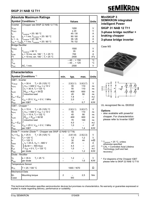
µV & 7M & 9&( 9 9*( 9 ,& $
ms31nab12t11.xls - 3
ms31nab12t11.xls - 4
Eon
15
Eon
10 Eoff 5 E 0 0 IC 20 40 60 A 80 E
10
5
Eoff
0LQL6.LL3
6.LL3 1$% 7 6.LL3 1$% 7 6.LL3 1$% 7
E\ 6(0,.521
7ROHUDQ.H ,62 I
E\ 6(0,.521
元器件交易网
6.LL3 1$% 7
70 A 60 50 40 30 20 10 IC 0 0 VCE 1 2 3 17V 15V 13V 11V 9V 7V
ms31nab12t11.xls - 1
70 A 60 50 40 30 20 10 IC 0 17V 15V 13V 11V 9V 7V
)LJ 7\S IUHHZKHHOLQJ GLRGH IRUZDUG .KDUD.WHULVWL.
E\ 6(0,.521
)LJ )RUZDUG .KDUD.WHULVWL. RI WKH LQSXW EULGJH GLRGH
元器件交易网
&DVH 0
%ULGJH 5H.WLILHU 7KHDWVLQN & WS PV VLQ 7M WS PV VLQ 7M
& &
$& PLQ
&KDUD.WHULVWL.V
6\PERO &RQGLWLRQV
SKIIP1242GB120-4D中文资料
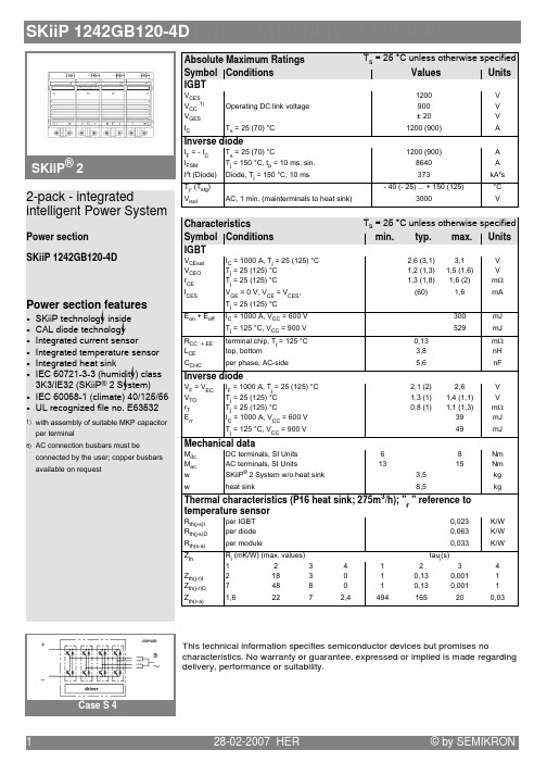
This technical information specifies semiconductor devices but promises no characteristics. No warranty or guarantee, expressed or implied is made regarding delivery, performance or suitability.
1
/
min. typ. max. Units
: :<
8 # C 7B 8 ", &#",' 9 7B 8 ", &#",' 9 7B 8 ", &#",' 9
:? 8 :C : 8 :C
7B 8 ", &#",' 9
28-02-2007 HER
© by SEMIKRON
元器件交易网
SKiiP 1242GB120-4D INTEGRATED DRIVER, SENSORS
SKiiP® 2
Absolute Maximum Ratings Symbol Conditions
:# :" :J
C
=$2 5
& '
<5
<5
5
5( :< :#" /1 / 7 &7 '
2.
#, : 1
msc1210中文
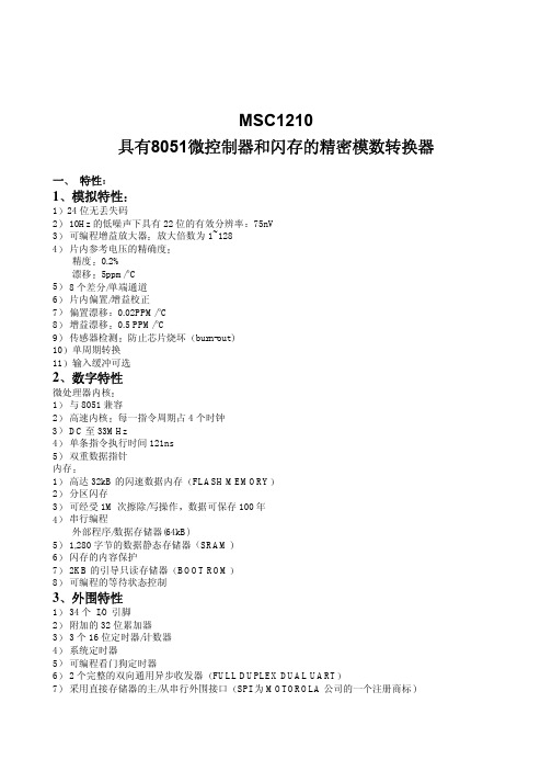
参数
模拟输入 AIN0-AIN7 AINCOM 模拟输入范
围
全输入电压范围 差分输入阻抗
输入电流 带宽
快速沉积滤波器 Sinc2滤波器 Sinc2滤波器
可编程增益放大器 输入电容 输入漏电流 熔断电流
偏移DAC 偏移DAC范围 偏移DAC单调性 偏移DAC增益偏差 偏移DAC增益偏差漂移
条件
缓冲区关闭 缓冲区打开 IN+ - IN- 看图4 缓冲区关闭 缓冲区打开
256
内部 MOVX 静态随机存储器 字节 1024
1024
1024
1024
数
外部可存取存储器 字节数
程序 64K 数据 64K
程序 64K 数据 64K
程序 64K 数据 64K
程序 64K 数据 64K
注释 1 所有器件的外围特性相同 仅闪存容量不同 2 类型号的最后一位数字代表片内闪存容量 的大小= 2N KB
DC下 fCM = 60Hz, fDATA = 10Hz fCM = 50Hz, fDATA = 50Hz fCM = 60Hz, fDATA = 60Hz fSIG = 50Hz, fDATA = 50Hz fSIG = 60Hz, fDATA = 60Hz
DC下 dB =–20log( VOUT/ VDD)
MSC1210YX
最小值
典型值
最大值
单位
AGND-0.1 AGND
1
5/PGA 0.5
AVDD+0.1
AVDD-1.5
+VREF/PGA
0.469 • fDATA 0.318 • fDATA 0.262 • fDATA
9 0.5 +6
128
SK9822 双信号传输灯珠 规格书

SK9822规格书智能外控(双线传输)表面贴装SMD 型LED文件编号: SPC/ SK9822产品型号: SK9822产品描述: 5.5x5.0x1.6毫米0.2瓦特智能外控双线传输表面贴装型SMD LED版本号.: 01日期: 2016-03-09ELECTROSTATICSENSITIVE DEVICES智能外控(双线传输)表面贴装SMD型LED 型号: SK98221.产品概述:SK9822是一款双线传输三通道(RGB)驱动控制电路与发光电路于一体的智能外控LED光源。
产品内含有信号解码模块、数据缓存器、内置恒流电路及RC振荡器;CMOS制程,低压、低耗电;256级PWM灰度调整及32级亮度调整;采用双线输出方式,DATA数据及同步的CLK讯号,使串接各晶片之输出动作同步;2.主要应用领域:● LED全彩发光字灯串,LED全彩模组,LED幻彩软硬灯条,LED护栏管,LED外观/情景照明● LED点光源,LED像素屏,LED异形屏,各种电子产品,电器设备跑马灯。
3.特性说明:● Top SMD内部集成高质量串行级联恒流IC;5V电源应用;默认上电不亮灯;● 控制电路与芯片集成在SMD 5050元器件中,构成一个完整的外控像素点,色温效果均匀且一致性高。
● 双线式同步控制。
● RGB三色输出控制,8Bit(256级)色彩设定;5Bit(32级)亮度调整;● 三路恒流驱动,具体信号自我检测功能● 最大串行输入数据频率30MHZ● 双线数据传输,内建振荡支持不间断PWM输出,可维持画面静止。
4.机械尺寸:备注:1. 以上标示单位为毫米.2. 除非另外注明,尺寸公差为±0.1毫米.5. 引脚图及功能序号符号管脚名功能描述1SDI数据输入串接资料输入端2CKI时钟输入串接时钟信号输入端3GND 地或电源负端电源负极4VCC 供电电源正端电源正极5CKO时钟输出串接时钟信号输出端6SDO数据输出串接资料输出端6. 产品命名一般说明SK9822SK9822: 默认为RGB晶片与IC集成在一起6.电气参数(极限参数,Ta=25℃,VSS=0V):参数符号范围单位-0.5~+5.5 V 电压电压VDD-0.3~VDD+0.3 V 逻辑输入电压VIN工作温度Topt -20~+80 ℃储存温度Tstg-50~+125 ℃ESD耐压V4K VESD7. 电气参数(如无特殊说明,TA=-20~+70℃,VDD=4.5~5.5V,VSS=0V):参数符号最小典型最大单位测试条件芯片内部电源电压V--- 5.0 5.3 V ---DD最大LED输出电I om ax --- --- 20 m A ----流时钟高电平宽度TCLKH--- --- >30 ns--- 时钟低电平宽度TCLKL--- --- >30 ns--- 数据建立时时间TSETUP--- --- >10 ns--- PWM频率F--- 1.2 --- KHZ---PWM静态功耗I--- 1--- m A ---DD8. 功能说明(1)串接资料结构(2)256级灰度数值占空比MSB……..LSB0000 0000 0 / 2560000 0001 1 / 2560000 0010 2 / 256- -- -- -- -- -1111 1101 253 / 2561111 1110 254 / 2561111 1111 255 / 256(3)PWM输入输出信号关系:(4)5-Bit(32级)亮度调整(同时控制OUTR\OUTG\OUTB三个端口的电流:数值电流调整MSB……..LSB00000 0 / 3100001 1 / 3100010 2 / 31- -- -- -- -- -11101 29 / 3111110 30 / 3111111 31 / 31(5)刷新率:帧频=1/((64+(32*点数))*CKI周期) (单位:帧/秒)如:1024个点、CKI 频率为1MHZ, 则帧频=30帧/秒。
开关电源芯片VIPER12简介
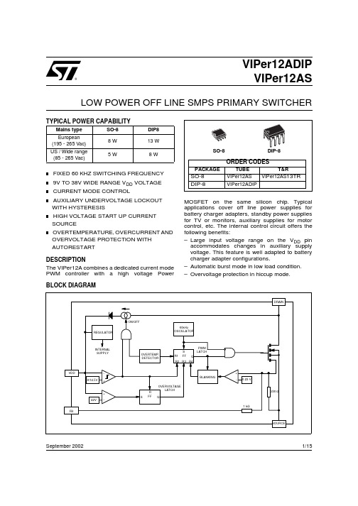
DRAIN
ON/OFF REGULATOR 60kHz OSCILLATOR
INTERNAL SUPPLY
OVERTEMP. DETECTOR
R1
S FF
PWM LATCH Q
R2 R3 R4
VDD 8/14.5V
_ BLANKING + OVERVOLTAGE LATCH Q
+ _ 0.23 V
+ 42V _ S
100 50 40
Note: 1. On clamped inductive load
3/15
VIPer12ADIP / VIPer12AS
ELECTRICAL CHARACTERISTICS (Tj=25°C, VDD=18V, unless otherwise specified) SUPPLY SECTION
Note: 1. This parameter applies when the start up current source is off. This is the case when the VDD voltage has reached VDDon and remains above VDDoff. 2. This parameter applies when the start up current source is on. This is the case when the VDD voltage has not yet reached VDDon or has fallen below V DDoff.
SO-8 DIP-8
TUBE T&R VIPer12AS VIPer12AS13TR VIPer12ADIP
n HIGH VOLTAGE START UP CURRENT n OVERTEMPERATURE, OVERCURRENT AND
MT9122资料
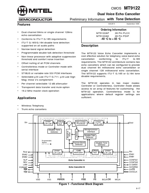
8-17DescriptionThe MT9122 Voice Echo Canceller implements a cost effective solution for telephony voice-band echo cancellation conforming to ITU-T G.165requirements. The MT9122 architecture contains two echo cancellers which can be configured to provide dual channel 64 millisecond echo cancellation or single channel 128 millisecond echo cancellation.The MT9122 supports ITU-T G.165 or G.164 tone disable requirements.The MT9122 operates in two major modes:Controller or Controllerless. Controller mode allows access to an array of features for customizing the MT9122 operation. Controllerless mode is for applications where default register settings are sufficient.Features•Dual channel 64ms or single channel 128ms echo cancellation•Conforms to ITU-T G.165 requirements •ITU-T G.165/G.164 disable tone detection supported on all audio paths •Narrow-band signal detection•Programmable double-talk detection threshold •Non-linear processor with adaptive suppression threshold and comfort noise insertion •Offset nulling of all PCM channels•Controllerless mode or Controller mode with serial interface•ST-BUS or variable-rate SSI PCM interfaces •Selectable µ/A-Law ITU-T G.711;µ/A-Law Sign Mag; linear 2’s complement•Per channel selectable 12 dB attenuator •Transparent data transfer and mute option •19.2 MHz master clock operationApplications•Wireless Telephony •Trunk echo cancellersFigure 1 - Functional Block DiagramLinear/µ/A-Law+Non-Linear ProcessorOffset NullLinear/µ/A-Law Linear/µ/A-LawMicroprocessorInterface Double-Talk DetectorDisable Tone Detector A d a p t i v e F i l t e rC o n t r o lNarrow-Band DetectorLinear/µ/A-LawOffset Null12dB AttenuatorEcho Canceller A Echo Canceller BVDD VSS PWRDN IC F0od F0i BCLK/C4i MCLKSoutRin ENA1ENB1CONFIG1CONFIG2S1/DA TA1S2/DA TA2S3/CS S4/SCLKSinRout ENA2ENB2NLP REV LAW FORMATTD1TD2-Programmable BypassDisable Tone Detector ISSUE 5September 1996Ordering Information MT9122AP 28 Pin PLCC MT9122AE 28 Pin PDIP-40°C to + 85°CMT9122Dual Voice Echo Cancellerwith Tone DetectionCMOSPreliminary InformationMT9122Preliminary Information8-18Figure 2 - Pin ConnectionsPin DescriptionPin #Name Description1ENA1SSI Enable Strobe / ST -BUS Mode for Rin/Sout (Input). This pin has dual functions depending on whether SSI or ST -BUS is selected.For SSI, this strobe must be present for frame synchronization. This is an active high channel enable strobe, 8 or 16 data bits wide, enabling serial PCM data transfer for Echo Canceller A on Rin/Sout pins. Strobe period is 125 microseconds.For ST -BUS, this pin, in conjunction with the ENB1 pin, will select the proper ST -BUS mode for Rin/Sout pins (see ST -BUS Operation description). The selected mode applies to both Echo Canceller A and B.2ENB1SSI Enable Strobe / ST-BUS Mode for Rin/Sout (Input).This pin has dual functions depending on whether SSI or ST -BUS is selected.For SSI, this is an active high channel enable strobe, 8 or 16 data bits wide, enabling serial PCM data transfer for Echo Canceller B on Rin/Sout pins. Strobe period is 125 microseconds.For ST -BUS, this pin, in conjunction with the ENA1 pin, will select the proper ST -BUS mode for Rin/Sout pins (see ST -BUS Operation description). The selected mode applies to both Echo Canceller A and B.3ENA2SSI Enable Strobe / ST -BUS Mode for Sin/Rout (Input).This pin has dual functions depending on whether SSI or ST -BUS is selected.For SSI, this is an active high channel enable strobe, 8 or 16 data bits wide, enabling serial PCM data transfer for Echo Canceller A on Sin/Rout pins. Strobe period is 125 microseconds.For ST -BUS, this pin, in conjunction with the ENB2 pin, will select the proper ST -BUS mode for Sin/Rout pins (see ST -BUS Operation description). The selected mode applies to both Echo Canceller A and B.4ENB2SSI Enable Strobe / ST -BUS Mode for Sin/Rout (Input).This pin has dual functions depending on whether SSI or ST -BUS is selected.For SSI, this is an active high channel enable strobe, 8 or 16 data bits wide, enabling serial PCM data transfer for Echo Canceller B on Sin/Rout pins. Strobe period is 125 microseconds.For ST -BUS, this pin, in conjunction with the ENA2 pin, will select the proper ST -BUS mode for Sin/Rout pins (see ST -BUS Operation description). The selected mode applies to both Echo Canceller A and B.12345678910111213141516171819202827262524232221S2/DA TA2VDD F0odIC TD1S1/DA TA1S4/SCLK Sout Rout BCLK/C4i CONFIG1CONFIG2Sin Rin NLP VSS ENB2ENB1F0i FORMA T REV LAW ENA1PWRDNTD2ENA2MCLKS3/CS E N B 2E N B 1E N A 1E N A 2B C L K /C 4iC O N F I G 1C O N F I G 2IC Sin Rin NLP VSS REVMCLKF O R M A T L A W P W R D N T D 2T D 1S 4/S C L K S 3/C SS2/DA TA2VDD F0odS1/DA TA1Sout Rout F0i PLCC456789101125242322212019•32128272612131415161718PDIPPreliminary Information MT9122 Pin Description (continued)Pin #Name Description5Rin Receive PCM Signal Input (Input). 128 kbit/s to 4096 kbit/s serial PCM input stream. Data may be in either companded or 2’s complement linear format. Two PCM channels are time-multiplexed on this pin. These are the Receive Input reference channels for Echo CancellersA and B. Data bits are clocked in following SSI or ST-BUS timing requirements.6Sin Send PCM Signal Input (Input). 128 kbit/s to 4096 kbit/s serial PCM input stream. Data may be in either companded or 2’s complement linear format. Two PCM channels are time-multiplexed on this pin. These are the Send Input channels (after echo path) for EchoCancellers A and B. Data bits are clocked in following SSI or ST-BUS timing requirements.7VSS Digital Ground: Nominally 0 volts.8MCLK Master Clock (Input): Nominal 20 MHz Master Clock input. May be connected to anasynchronous (relative to frame signal) clock source.9IC Internal Connection (Input): Must be tied to Vss.10NLP Non-Linear Processor Control (Input):Controllerless Mode:An active high enables the Non-Linear Processors in Echo Cancellers Aand B. Both NLP’s are disabled when low. Intended for conformance testing to G.165 and it isusually tied to Vdd for normal operation.Controller Mode: This pin is ignored (tie to Vdd or Vss). The non-linear processor operation iscontrolled by the NLPDis bit in Control Register 2. Refer to the Register Summary.11REV Reversal Detection (Input):Controllerless Mode:An active high configures all the tone detectors to trigger only when a2100Hz disable tone with periodic phase reversal is present (per G.165). When low, the tonedetectors will trigger upon detection of any 2100Hz disable tone, with or without periodicphase reversal (per G.164).Controller Mode:This pin is ignored (tie to VDD or VSS). The operation is controlled by thePHDis bit in Control Register 2. Refer to the Register Summary.12LAW A/µ Law Select (Input):An active low selectsµ−Law companded PCM. When high, selects A-Law companded PCM.This control is for both echo cancellers and is valid for both controller and controllerlessmodes.13FORMAT ITU-T/Sign Mag (Input):An active low selects sign-magnitude PCM code. When high, selects ITU-T (G.711) PCMcode. This control is for both echo cancellers and is valid for both controller and controllerlessmodes.14PWRDN Power-down (Input): An active low resets the device and puts the MT9122 into a low-power stand-by mode.15TD2Tone Detect 2 (Output):An active low output occurs when Echo Canceller B detects the presence of a valid 2100Hzdisabling tone (G.164 or G.165) on Rin or Sin pins. This output returns to a logic high once therelease criteria are met. The behavior of this pin is identical in both controller andcontrollerless modes.16TD1Tone Detect 1 (Output):An active low output occurs when Echo Canceller A detects the presence of a valid 2100Hzdisabling tone (G.164 or G.165) on Rin or Sin pins. This output returns to a logic high once therelease criteria are met. The behavior of this pin is identical in both controller andcontrollerless modes.8-19MT9122Preliminary Information8-20Notes:1.All unused inputs should be connected to logic low or high unless otherwise stated. All outputs should be left open circuit when not used.2.All inputs have TTL compatible logic levels except for MCLK, Sin and Rin pins which have CMOS compatible logic levels and PWRDN pin which has Schmitt trigger compatible logic levels.3.All outputs are CMOS pins with CMOS logic levels.17/181718S4/S3SCLK CS Selection of Echo Canceller B Functional States (Input):Controllerless Mode: Selects Echo Canceller B functional states according to Table 2.Controller Mode: S4 and S3 pins become SCLK and CS pins respectively.Serial Port Synchronous Clock (Input): Data clock for the serial microport interface.Chip Select (Input): Enables serial microport interface data transfers. Active low.19/201920S2/S1DATA2DATA1Selection of Echo Canceller A Functional States (Input):Controllerless Mode: Selects Echo Canceller A functional states according to Table 2.Controller Mode: S2 and S1 pins become DATA2 and DATA1 pins respectively.Serial Data Receive (Input):In Motorola/National serial microport operation, the DA TA2 pin is used for receiving data. In Intel serial microport operation, the DATA2 pin is not used and must be tied to Vss or Vdd.Serial Data Port (Bidirectional):In Motorola/National serial microport operation, the DATA1 pin is used for transmitting data. In Intel serial microport operation, the DATA1 pin is used for transmitting and receiving data.21F0odDelayed Frame Pulse Output (Output):In ST -BUS operation, this pin generates a delayed frame pulse after the 4th channel time slot and is used for daisy-chaining multiple ST -BUS devices. See Figures 5 to 8.In SSI operation, this pin outputs logic low.22VDD Positive Power Supply: Nominally 5 volts.23SoutSend PCM Signal Output (Output):128 kbit/s to 4096 kbit/s serial PCM output stream. Data may be in either companded or 2’s complement linear PCM format. T wo PCM channels are time-multiplexed on this pin. These are the Send Out signals after echo cancellation and Non-linear processing. Data bits are clocked out following SSI or ST -BUS timing requirements.24RoutReceive PCM Signal Output (Output):128 kbit/s to 4096 kbit/s serial PCM output stream. Data may be in either companded or 2’s complement linear PCM format. T wo PCM channels are time-multiplexed on this pin. This output pin is provided for convenience in some applications and may not always be required.Data bits are clocked out following SSI or ST -BUS timing requirements.25F0iFrame Pulse (input):In ST -BUS operation, this is a frame alignment low going pulse. SSI operation is enabled by connecting this pin to Vss.26BCLK/C4i Bit Clock/ST -BUS Clock (Input):In SSI operation, BCLK pin is a 128 kHz to 4.096 MHz bit clock. This clock must be synchronous with ENA1, ENA2, ENB1 and ENB2 enable strobes.In ST -BUS operation,C4i pin must be connected to the 4.096MHz (C4) system clock.27/28CONFIG1/CONFIG2Device Configuration Pins (Inputs).When CONFIG1 and CONFIG2 pins are both logic 0, the MT9122 serial microport is enabled.This configuration is defined as Controller Mode. When CONFIG1 and CONFIG2 pins are in any other logic combination, the MT9122 is configured in Controllerless Mode. See Table 3.Pin Description (continued)Pin #Name DescriptionPreliminary InformationMT91228-21Functional DescriptionThe MT9122 architecture contains two individually controlled echo cancellers (Echo Canceller A and B).They can be set in three distinct configurations:Normal, Back-to-Back and Extended Delay (see Figure 3). Under Normal configuration, the two echo cancellers are positioned in parallel providing 64millisecond echo cancellation in two channels simultaneously. In Back-to-Back configuration, the two echo cancellers are positioned to cancel echo coming from both directions in a single channel. In Extended-Delay configuration, the two echo cancellers are internally cascaded into one 128millisecond echo canceller.Each echo canceller contains the following main elements (see Figure 1).•Adaptive Filter for estimating the echo channel •Subtracter for cancelling the echo•Double-Talk detector for disabling the filter adaptation during periods of double-talk •Non-Linear Processor for suppression of residual echo•Disable Tone Detectors for detecting valid disable tones at the input of receive and send paths•Narrow-Band Detector for preventing Adaptive Filter divergence caused by narrow-band signals•Offset Null filters for removing the DC component in PCM channels•12dB attenuator for signal attenuation •Serial controller interface compatible with Motorola, National and Intel microcontrollers •PCM encoder/decoder compatible with µ/A-Law ITU-T G.711,µ/A-Law Sign-Mag or linear 2’s complement codingThe MT9122 has two modes of operation:Controllerless and Controller . Controllerless mode is intended for applications where customization is not required. Controller mode allows access to all registers for customizing the MT9122 operation.Refer to Table 7 for a complete list. Controller mode is selected when CONFIG1 and CONFIG2 pins are both connected to Vss.Each echo canceller in the MT9122 has four functional states:Mute ,Bypass ,Disable Adaptation and Enable Adaptation . These are explained in the section entitled Echo Canceller Functional States.Figure 3 - Device ConfigurationRinRoutSoutSin echo path AOptional -12dB padPORT 2PORT 1echo path B+-channel Achannel A+-channel Bchannel BE.C.A E.C.Ba) Normal Configuration (64ms)+-channel Achannel AE.C.ASin SoutRoutRinb) Extended Delay Configuration (128ms)PORT 2PORT 1+E.C.ASinSoutRoutRin c) Back-to-Back Configuration (64ms)- E.C.B+-echo echo pathpathPORT 2PORT 1echo path AAdaptive Filter (64ms)Adaptive Filter (64ms)Optional -12dB pad Adaptive Filter (64ms)Optional -12dB padAdaptive Filter (64ms)Optional -12dB padAdaptive Filter (128 ms)Optional -12dB padMT9122Preliminary InformationAdaptive FilterThe adaptive filter is a 1024 tap FIR filter which is divided into two sections. Each section contains 512 taps providing 64ms of echo estimation. In Normal configuration, the first section is dedicated to channel A and the second section to channel B. In Extended Delay configuration, both sections are cascaded to provide 128ms of echo estimation in channel A.Double-Talk DetectorDouble-Talk is defined as those periods of time when signal energy is present in both directions simultaneously. When this happens, it is necessary to disable the filter adaptation to prevent divergence of the adaptive filter coefficients. Note that when double-talk is detected, the adaptation process is halted but the echo canceller continues to cancel echo.A double-talk condition exists whenever the Sin signal level is greater than the expected return echo level. The relative signal levels of Rin (Lrin) and Sin (Lsin) are compared according to the following expression to identify a double-talk condition:Lsin > Lrin + 20log10(DTDT)where DTDT is the Double-Talk Detection Threshold. Lsin and Lrin are the relative signal levels expressed in dBm0.A different method is used when it is uncertain whether Sin consists of a low level double-talk signal or an echo return. During these periods, the adaptation process is slowed down but it is not halted.Controllerless ModeIn G.165 standard, the echo return loss is expected to be at least 6dB. This implies that the Double-Talk Detector Threshold (DTDT) should be set to 0.5 (-6dB). However, in order to get additional guardband, the DTDT is set internally to 0.5625 (-5dB). In controllerless mode, the Double-Talk Detector is always active.Controller ModeIn some applications the return loss can be higher or lower than 6dB. The MT9122 allows the user to change the detection threshold to suit each application’s need. This threshold can be set by writing the desired threshold value into the DTDT register.The DTDT register is 16 bits wide. The register value in hexadecimal can be calculated with the following equation:DTDT(hex) = hex(DTDT(dec) * 32768)where 0 < DTDT(dec) < 1Example:For DTDT = 0.5625 (-5dB), thehexadecimal value becomeshex(0.5625 * 32768) = 4800hNon-Linear Processor (NLP)After echo cancellation, there is always a small amount of residual echo which may still be audible. The MT9122 uses an NLP to remove residual echo signals which have a level lower than the Adaptive Suppression Threshold (TSUP in G.165). This threshold depends upon the level of the Rin (Lrin) reference signal as well as the programmed value of the Non-Linear Processor Threshold register (NLPTHR). TSUP can be calculated by the following equation:TSUP = Lrin + 20log10(NLPTHR)where NLPTHR is the Non-Linear Processor Threshold register value and Lrin is the relative power level expressed in dBm0.When the level of residual error signal falls below TSUP, the NLP is activated further attenuating the residual signal to less than -65dBm0. To prevent a perceived decrease in background noise due to the activation of the NLP, a spectrally-shaped comfort noise, equivalent in power level to the background noise, is injected. This keeps the perceived noise level constant. Consequently, the user does not hear the activation and de-activation of the NLP. Controllerless ModeThe NLP processor can be disabled by connecting the NLP pin to Vss.Controller ModeThe NLP processor can be disabled by setting the NLPDis bit to 1 in Control Register 2.The NLPTHR register is 16 bits wide. The register value in hexadecimal can be calculated with the following equation:NLPTHR(hex) = hex(NLPTHR(dec) * 32768)8-22Preliminary InformationMT91228-23where 0 < NLPTHR (dec) < 1The comfort noise injection can be disabled by setting the INJDis bit to 1 in Control Register 1.It should be noted that the NLPTHR is valid and the comfort noise injection is active only when the NLP is enabled.Disable Tone DetectorG.165 recommendation defines the disable tone as having the following characteristics: 2100 Hz (±21Hz) sinewave, a power level between -6 to -31dBm0, and a phase reversal of 180 degrees (±25degrees) every 450ms (±24ms). If the disable tone is present for a minimum of one second with at least one phase reversal, the Tone Detector will trigger.G.164 recommendation defines the disable tone as a 2100 Hz (±21Hz) sinewave with a power level between -6 to -31dBm0. If the disable tone is present for a minimum of one second, with or without phase reversal, the Tone Detector will trigger.The MT9122 has four Tone Detectors in order to monitor the occurrence of a valid disable tone on channels A and B on both Rin and Sin. Upon detection of a disable tone, output pins TD1 or TD2will go low as illustrated in Figure 4.Figure 4 - Disable Tone DetectionOnce a Tone Detector has been triggered, the MT9122 no longer needs a valid disable tone (G.164or G.165) to maintain Tone Detector status (e.g.TD1,TD2 pins low). The Tone Detector status will only release (e.g.TD1,TD2 pins high) if the signals Rin and Sin fall below -30dBm0, in the frequency range of 390Hz to 700Hz, and below -34dBm0, in the frequency range of 700Hz to 3400Hz, for at least 400ms.Controllerless ModeThe selection between G.165 and G.164 tone disable is controlled by the REV pin. When the REV pin is connected to Vss, G.164 is selected. This applies to all four Tone Detectors.In response to a valid disable tone, the MT9122 must be switched from the Enable Adaptation state to the Bypass state. In an application, the Tone Detect outputs,TD1 and TD2, may be used to switch the echo cancellers between these two states. This is achieved by connecting S1 and S3 pins to Vdd and by connecting the TD1 and TD2 outputs to the S2and S4 input pins respectively.Controller ModeThe selection between G.165 and G.164 tone disable is controlled by the PHDis bit in Control Register 2. When the PHDis bit is set to 1, G.164tone disable requirements are selected. This applies to all four Tone Detectors.In response to a valid disable tone, the MT9122 must be switched from the Enable Adaptation state to the Bypass state. This can be done in two ways,automatically or externally. In automatic mode, the Tone Detectors internally control the switching between Enable Adaptation and Bypass states. The automatic mode can be activated by setting the AutoTD bit in Control Register 2 to high. In external mode, an external controller is needed to poll the TD bit in Status Register A or B. Following the detection of a disable tone (TD bit high), the external controller should switch the echo canceller from Enable Adaptation to Bypass state.The TD1 and TD2 output pins remain active, as in Controllerless mode, and they can be used as an interrupt to an external controller.Narrow Band Signal Detector (NBSD)Single or dual frequency tones (e.g. DTMF tones)present in the reference input (Rin) of the echo canceller for a prolonged period of time may cause the adaptive filter to diverge. The Narrow Band Signal Detector (NBSD) is designed to prevent this divergence by detecting single or dual tones of arbitrary frequency, phase, and amplitude. When narrow band signals are detected, the adaptation process is halted but the echo canceller continues to cancel echo.TD1Rin SinEcho Canceller ATone Detector Tone Detector Echo Canceller BTD2Rin SinTone Detector Tone DetectorMT9122Preliminary InformationControllerless ModeThe NBSD is always active and automatically disables the filter adaptation process when narrow band signals are detected.Controller ModeThe NBSD can be disabled by setting the NBDis bit to 1 in Control Register 2.Offset Null FilterAdaptive filters in general do not operate properly when a DC offset is present on either the reference signal (Rin) or the echo composite signal (Sin). To remove the DC component, the MT9122 incorporates Offset Null filters in both Rin and Sin inputs.Controllerless ModeThe Offset Null filters are always active.Controller ModeThe offset null filters can be disabled by setting the HPFDis bit to 1 in Control Register 2.Echo Canceller Functional StatesEach echo canceller has four functional states: Mute, Bypass, Disable Adaptation and Enable Adaptation.Mute:The Mute state forces the echo canceller to transmit quiet code and halts the filter adaptation process.In Normal configuration, the PCM output data on Rout is replaced with the quiet code according to the following table.In Back-to-Back configuration, both echo cancellers are combined to implement a full duplex echo canceller. Therefore muting Echo Canceller A causes quiet code to be transmitted on Rout, while muting Echo Canceller B causes quiet code to be transmitted on Sout.In Extended Delay configuration, both echo cancellers are cascaded to make one 128ms echo canceller. In this configuration, muting Echo Canceller A causes quiet code to be transmitted on Rout.Bypass:The Bypass state directly transfers PCM codes from Rin to Rout and from Sin to Sout. When Bypass state is selected, the adaptive filter coefficients are reset to zero.Disable Adaptation:When the Disable Adaptation state is selected, the adaptive filter coefficients are frozen at their current value. In this state, the adaptation process is halted however the MT9122 continues to cancel echo. Enable Adaptation:In Enable Adaptation state, the adaptive filter coefficients are continually updated. This allows the echo canceller to model the echo return path characteristics in order to cancel echo. This is the normal operating state.Controllerless ModeThe four functional states can be selected via S1, S2, S3, and S4 pins as shown in the following table.(1) Filter coefficients are frozen (adaptation disabled)(2) The adaptive filter coefficients are reset to zero(3) The MT9122 cancels echoTable 2 - Functional States Control PinsController ModeThe echo canceller functions are selected in Control Register 1 and Control Register 2 through four control bits: MuteS, MuteR, Bypass and AdaptDis. See Register Summary for details.MT9122 Throughput DelayThe throughput delay of the MT9122 varies according to the data path and the device configuration. For all device configurations, except for Bypass state, Rin to Rout has a delay of two frames and Sin to Sout has a delay of three frames.LINEAR16 bits2’s complementSIGN/MAGNITUDEµ-LawA-LawCCITT (G.711)µ-Law A-Law+Zero(quiet code)0000h80h FFh D5h Table 1 - Quiet PCM Code AssignmentEchoCanceller AS2/S1Functional StateEchoCanceller BS4/S3 00Mute(1)0001Bypass(2)0110Disable Adaptation(1,3)1011Enable Adaptation(3)118-24Preliminary InformationMT91228-25In Bypass state, the Rin to Rout and Sin to Sout paths have a delay of two frames. In ST -BUS operation, the D and C channels have a delay of one frame.Power DownForcing the PWRDN pin to logic low, will put the MT9122 into a power down state. In this state all internal clocks are halted, the DATA1, Sout and Rout pins are tristated and the F0od,TD1, and TD2 pins output high.The device will automatically begin the execution of its initialization routines when the PWRDN pin is returned to logic high and a clock is applied to the MCLK pin. The initialization routines execute for one frame and will set the MT9122 to default register values.Device ConfigurationThe MT9122 architecture contains two individually controlled echo cancellers (Echo Canceller A and B).They can be set in three distinct configurations:Normal, Back-to-Back, and Extended Delay. See Figure 3.Normal Configuration:In this configuration, the two echo cancellers (Echo Canceller A and B) are positioned in parallel, as shown in Figure 3a, providing 64 milliseconds of echo cancellation in two channels simultaneously.In SSI operation, both channels are available in different timeslots on the same TDM (Time Division Multiplexing) bus. For Echo Canceller A, the ENA1enable strobe pin defines the Rin/Sout (PORT1) time slot while the ENA2 enable strobe pin defines the Sin/Rout (PORT2) time slot. The ENB1 and ENB2enable strobes perform the same function for Echo Canceller B.In ST -BUS operation, the ENA1, ENA2, ENB1 and ENB2 pins are used to determine the PCM data format and the channel locations. See Table 4.Back-to-Back Configuration:In this configuration, the two echo cancellers are positioned to cancel echo coming from both directions in a single channel providing full duplex 64millisecond echo-cancellation. See Figure 3c. This configuration uses only one timeslot on PORT1 and PORT2, allowing a no-glue interface for applications where bidirectional echo cancellation is required.In SSI operation, ENA1 and ENA2 enable pins are used to strobe data on Rin/Sout and Sin/Rout respectively. In ST -BUS operation, ENA1, ENA2,ENB1 and ENB2 inputs are used to select the ST -BUS mode according to Table 4.Examples of Back-to-Back configuration include positioning the MT9122 between a codec and a transmission device or between two codecs for echo control on analog trunks.Extended Delay configuration:In this configuration, the two echo cancellers are internally cascaded into one 128 millisecond echo canceller. See Figure 3b. In SSI operation, ENA1and ENA2 enable pins are used to strobe data on Rin/Sout and Sin/Rout respectively. In ST -BUS operation, ENA1, ENA2, ENB1 and ENB2 inputs are used to select the ST -BUS mode according to Table 4.Controllerless ModeThe three configurations can be selected through the CONFIG1 and CONFIG2 pins as shown in the following table.Table 3 - Configuration in Controllerless ModeController ModeIn Control Register 1, the Normal configuration can be programmed by setting both BBM and Extended-Delay bits to 0. Back-to-Back configuration can be programmed by setting the BBM bit to 1 and Extended-Delay bit to 0. Extended-Delay configuration can be programmed by setting the Extended-Delay bit to 1 and BBM bit to 0. Both BBM and Extended-Delay bits in Control Register 1 can not be set to 1 at the same time.PCM Data I/OThe PCM data transfer for the MT9122 is provided through two PCM ports.PORT1 consists of Rin and Sout pins while PORT2 consists of Sin and Rout Pins.The Data is transferred through these ports according to either ST -BUS or SSI conventions. The device determines the mode of operation by monitoring the signal applied to the F0i pin. When aCONFIG1CONFIG2CONFIGURATION00(selects Controller Mode)01Extended Delay Mode 10Back-to-Back Mode 11Normal Mode。
自学习型无线解码芯片SK202Rev1.2

⾃学习型⽆线解码芯⽚SK202Rev1.2⾃学习型⽆线解码芯⽚SK202主要特性:☆智能学习,⽆需编码☆兼容市⾯⼤多数固定码编码芯⽚:如PT2262、SC2262、EV1527等☆⾃动适应发射端振荡电阻☆集互锁、⾃锁、点动三种功能⼀体,代替PT2272系列:L4、M4、T4,通过跳线选择☆⽀持4位数据码的输出,并且有VT输出☆内置存储器,更安全更可靠☆内置⾼精度振荡器,不需外接晶振☆⽀持1-20组地址码的学习存储☆宽⼯作电压:3.6-5.5V☆低⼯作电流:<5mA☆提供SOP14L封装⼀、SK202引脚功能说明引脚名称功能说明1 M4 M4模式选择,与Vss短接2 T4 T4模式选择,与Vss短接3 Vdd 电源正极,3.6-5.5V供电4 Vss 电源负极5 NC 悬空,不能外接电路6 MODE 发射编码选择,悬空⽀持PT2262,与Vss短接⽀持EV15277 D3 输出端D38 D0 输出端D09 D1 输出端D110 D2 输出端D211 VT 解码有效确认输出,有效解码时输出⾼电平12 KEY 学习编码按键输⼊,通过按键与Vss连接13 LED 学习状态指⽰灯,连接1K电阻和LED,到Vss14 RF RF信号输⼊端,接到⽆线接收模块的输出注1:M4和T4都悬空:解码模式为L4M4短接Vss,T4悬空,解码模式为M4M4悬空,T4短接Vss,解码模式为T4解码模式L4/M4/T4定义:L4 –输出锁存型按发射按钮,对应的输出端输出⾼电平并⼀直保持M4-输出暂存型按发射按钮,对应的输出端输出⾼电平,在停⽌发射后,恢复为低电平T4-输出触发型每按⼀次发射按钮,对应的输出端输出状态翻转⼀次2:引脚5需要悬空⼆、应⽤电路三、操作说明1、学习遥控器编码:按下学习按键,学习状态灯会亮,此时按下遥控器上任意⼀下按键,学习状态灯会闪2下,表⽰学习成功,遥控器可以进⾏正常解码控制。
SK202最多可以保存20组遥控发射器编码,超过20组时,最先学习的⼀组编码会被清除。
- 1、下载文档前请自行甄别文档内容的完整性,平台不提供额外的编辑、内容补充、找答案等附加服务。
- 2、"仅部分预览"的文档,不可在线预览部分如存在完整性等问题,可反馈申请退款(可完整预览的文档不适用该条件!)。
- 3、如文档侵犯您的权益,请联系客服反馈,我们会尽快为您处理(人工客服工作时间:9:00-18:30)。
自学习型无线解码芯片SK212
主要特性:
☆兼容市面大多数固定码编码芯片:如PT2262、PT2242、EV1527等
☆集锁存、暂存、互锁、翻转四种功能一体,通过跳线选择
☆支持PT2262(三态地址码)和EV1527(20位地址码)遥控器混合学习
☆支持4位数据码的输出,并且有VT输出
☆内置高精度振荡器,不需外接晶振
☆ 自动适应发射端振荡电阻
☆智能学习,无需手工编码
☆内置存储器,更安全更可靠
☆最多支持39个遥控器学习
☆超宽工作电压:2.6-5.5V
☆工业温度范围:-40~85℃
☆低工作电流:≈3mA
☆提供SOP14L封装
一、SK212引脚功能说明
引脚名称功能说明
1 GND 电源负极
2 KEY 学习按键输入,通过按键与GND连接
3 VT 解码有效输出口,解码有效时输出高电平
4 D0 数据输出端D0
5 D1 数据输出端D1
6 D2 数据输出端D2
7 D3 数据输出端D3
8 NC 悬空,待扩展
9 NC 悬空,待扩展
10 LED 学习状态指示灯
11 M1 输出模式选择M1(内置上位电阻)
12 M2 输出模式选择M2(内置上位电阻)
13 RF RF信号输入端,接到无线接收模块的DA TA
14 VCC 电源正极,2.6-5.5V供电
二、应用电路
输出模式说明:
模式 M1 M2 说明
锁存
H
H
对应的输出端输出高电平并一直保持,支持15种输出状态 通过判断VT 识别有效信号
暂存 H L
对应的输出端输出高电平,在停止发射后恢复低电平,支持15种输出状态
翻转 L H
每按一次发射按钮,对应的输出端输出状态翻转一次,只支持4按键遥控器的单按键操作
互锁 L L
对应的输出端输出高电平并一直保持,只支持4按键遥控器的单按键操作,D0-D3输出只有一个高电平
三、操作说明
1、学习EV1527编码遥控器:
按下学习按键1次,学习状态灯常亮,进入学习遥控编码状态,此时按下遥控器上任意按键,学习状态灯快速闪2下,表示学习成功。
对于已经学习过的遥控器,无法再次学习。
注:EV1527编码是指有20位地址码的学习码,包括EV1527、EV527、SC1527、HS1527、RT1527、PT2240等芯片。
2、学习PT2262编码遥控器:
按下学习按键1次,学习状态灯常亮,进入学习遥控编码状态,此时按下遥控器上任意按键,学习状态灯快速闪2下,表示学习成功。
对于已经学习过的遥控器,无法再次学习。
注:PT2262编码是指有8位三态地址码的编码,包括PT2262,PT2260,PT2264等芯片。
3、退出学习状态
进入学习状态30秒未成功学习,会自动退出学习状态。
或者按下第2次按键时退出学习。
注:SK212智能识别遥控器编码芯片是PT2262还是EV1527,不需要手动选择。
4、清除编码
SK212最多可以保存39组遥控发射器编码,超过39组时,最先学习的一组编码会被覆盖。
按下学习按键不放5秒钟,所有编码都被清除,学习状态灯闪烁6秒,表示清除编码成功。
LED显示与对应的功能
LED 功能
常亮等待学习状态
快速闪2下学习成功
快速闪6下清除编码成功
熄灭正常等待解码状态
5、振荡电阻选择
SK212采用智能识别技术,智能匹配发射端芯片PT2262及EV1527芯片的速率电阻大小。
6、解码输出方式选择
通过M1、M2的高低电平设置,可以选择4种输出模式,改变输出模式后,必须重新上电才能生效。
具体功能见上页表格说明。
通过引脚电平选择输出模式,更可靠,更直观。
防止按键选择带来的误操作已损坏机器。
7、数据输出口说明
SK212的D0、D1、D2、D3为输出口,它们的电平和遥控器上的PT2262或者EV1527的数据口状态是对应的,遥控按键哪个数据口为高电平,SK212解码后对应的数据口即为高电平。
完美替代PT2272并增加更多的功能。
四、与SK202性能对比
SK212与SK202对比
项目SK212 SK202 说明
工作电压 2.6~5.5V 3.6~5.5V 更宽工作电压,适合3V/5V供电输出模式4种3种增加互锁模式
编码选择智能识别引脚选择智能识别更方便
混合学习支持不支持EV1527和PT2262可混合学习学习数量39组80组学习遥控器少些封装SOP14L SOP14L 引脚数目不变,引脚功能改变
五、电气特性
(VCC=5V,TA=25℃,除非另有说明)
参数最小值典型值最大值单位测试条件工作电压 2.6 5.0 5.5 V
工作电流 3.0 5.0 mA TA= -40~85℃输出电流
5 mA V out=4.7V
IOH
灌入电流
10 mA V out=0.4V
IOL
工作温度-40 85 ℃
储存温度-55 125 ℃
数据保存10 Year TA= -40~85℃
六、封装信息
七、技术支持
公司网址:/
公司地址:广东省佛山市顺德区大良锦绣路圣景花园22座
支持热线:
联 系 人:李日辉(总工程师)
更新历史:
版本号 更新日期 更新内容 Rev1.0 2013.11.1 初稿。
