DS1621温度传感器实验
大学物理实验-温度传感器实验报告

关于温度传感器特性的实验研究摘要:温度传感器在人们的生活中有重要应用,是现代社会必不可少的东西。
本文通过控制变量法,具体研究了三种温度传感器关于温度的特性,发现NTC电阻随温度升高而减小;PTC电阻随温度升高而增大;但两者的线性性都不好。
热电偶的温差电动势关于温度有很好的线性性质。
PN节作为常用的测温元件,线性性质也较好。
本实验还利用PN节测出了波尔兹曼常量和禁带宽度,与标准值符合的较好。
关键词:定标转化拟合数学软件EXPERIMENTAL RESEARCH ON THE NATURE OF TEMPERATURE SENSOR1.引言温度是一个历史很长的物理量,为了测量它,人们发明了许多方法。
温度传感器通过测温元件将温度转化为电学量进行测量,具有反应时间快、可连续测量等优点,因此有必要对其进行一定的研究。
作者对三类测温元件进行了研究,分别得出了电阻率、电动势、正向压降随温度变化的关系。
2.热电阻的特性2.1实验原理2.1.1Pt100铂电阻的测温原理和其他金属一样,铂(Pt)的电阻值随温度变化而变化,并且具有很好的重现性和稳定性。
利用铂的此种物理特性制成的传感器称为铂电阻温度传感器,通常使用的铂电阻温度传感器零度阻值为100Ω(即Pt100)。
铂电阻温度传感器精度高,应用温度范围广,是中低温区(-200℃~650℃)最常用的一种温度检测器,本实验即采用这种铂电阻作为标准测温器件来定标其他温度传感器的温度特性曲线,为此,首先要对铂电阻本身进行定标。
按IEC751国际标准,铂电阻温度系数TCR定义如下:TCR=(R100-R0)/(R0×100) (1.1)其中R100和R0分别是100℃和0℃时标准电阻值(R100=138.51Ω,R0=100.00Ω),代入上式可得到Pt100的TCR为0.003851。
Pt100铂电阻的阻值随温度变化的计算公式如下:Rt=R0[1+At+B+C(t-100)] (-200℃<t<0℃) (1.2)式中Rt表示在t℃时的电阻值,系数A、B、C为:A=3.908×;B=-5.802×;C=-4.274×。
数字温度传感器DS1621及其应用
DS1621是DALLAS公司生产的一种功能较强的数字式温度传感器和恒温控制器。
与同系列的DS1620相比控制更为简单,接口与I2C总线兼容,且可以使用一片控制器控制多达8片的DS1621。
其数字温度输出达9位,精度为0.5℃。
通过读取内部的计数值和用于温度补偿的每摄氏度计数值,利用公式计算还可提高温度值的精度。
DS1621可工作在最低2.7V 电压下,适用于低功耗应用系统。
利用DS1621和一片2051单片机即可构成一个简洁但功能强大的低电压温度测量控制系统。
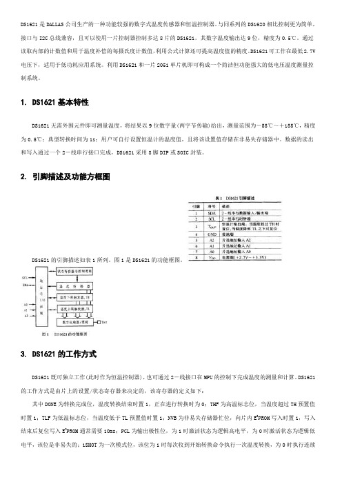
1. DS1621基本特性DS1621无需外围元件即可测量温度,将结果以9位数字量(两字节传输)给出,测量范围为-55℃~+155℃,精度为0.5℃;典型转换时间为1s;用户可自行设置恒温计的温度值,且将该设置值存储在非易失存储器中。
数据的读出和写入通过一个2-线串行接口完成,DS1621采用8脚DIP或SOIC封装。
2. 引脚描述及功能方框图DS1621的引脚描述如表1所列。
图1是DS1621的功能框图。
3. DS1621的工作方式DS1621既可独立工作(此时作为恒温控制器),也可通过2-线接口在MPU的控制下完成温度的测量和计算。
DS1621的工作方式是由片上的设置/状态寄存器来决定的,该寄存器的定义如下:其中DONE为转换完成位,温度转换结束时置1,正在进行转换时为0;THF为高温标志位,当温度超过TH预置值时置1;TLF为低温标志位,当温度低于TL预置值时置1;NVB为非易失存储器忙位,向片内E2PROM写入时置1,写入结束后复位写入E2PROM通常需要10ms;PCL为输出极性位,为1时激活状态为逻辑高电平,为0时激活状态为逻辑低电平,该位是非易失的;1SHOT为一次模式位,该位为1时每次收到开始转换命令执行一次温度转换,为0时执行连续温度转换,该位亦是非易失的。
DS1621在嵌入一个系统前,需由MPU将设置/状态寄存器值通过2-线接口写入该寄存器,之后DS1261或作为恒温计独立工作,或在MPU控制下进行温度测量和计算。
数字温度传感器DS1621在Linux下的ⅡC接口驱动设计
数字温度传感器DS1621在Linux下的ⅡC接口驱动设计朱瑜亮;黄晓革【期刊名称】《电子设计工程》【年(卷),期】2011(19)2【摘要】With widely use of the IIC bus and chips having IIC interface widely used in embedded system,this paper designed an IIC interface device driver under Linux operating system based on S3C2440 of ARM9 platform. According to the IIC bus protocol, this device driver accomplished configuration of digital temperature sensor DS1621 and obtained the temperature information in kernel space, then it transmittea the data back to the user space and printed it out. The result shows that the typical updating time is 1s, accuracy isl of a figure aftar decimal point. It also can establish a low voltage and low power consumption temperature test system hy using one more piece of DS1621. It would he broad applications in temperature monitoring of embedded devices.%针对目前ⅡC总线以及具有ⅡC接口的芯片在嵌入式系统中的广泛应用,设计了一种基于ARM9平台S3C2440的,Linux操作系统下的ⅡC接口设备驱动程序.通过ⅡC 总线协议,驱动程序实现了在内核状态下对数字温度传感器DS1621的配置和获取其温度信息,并将其传回用户空间并打印显示.实验结果表明,工作时典型数据更新时间为1 s.精度为小数点后一位.且利用多片DS1621可扩展一个低电压、低功耗的多点数字测温系统,在嵌入式设备的温度监测方面将有着广泛应用.【总页数】4页(P133-136)【作者】朱瑜亮;黄晓革【作者单位】电子科技大学,电子工程学院,四川,成都,610054;电子科技大学,电子工程学院,四川,成都,610054【正文语种】中文【中图分类】TP316【相关文献】1.Linux系统下PCIE to RapidIO桥驱动设计与实现 [J], 李红兵2.基于Linux的FPGA数据通信接口驱动设计与实现 [J], 蒋贵全;张辉;王国锋3.基于Linux的ARM与FPGA SPI接口驱动设计 [J], 陈少华4.基于Linux平台的PCI数据接口卡驱动设计 [J], 周磊;胡学龙5.基于嵌入式Linux的TII接口驱动设计 [J], 孙宝龙;解永平因版权原因,仅展示原文概要,查看原文内容请购买。
温度传感器DS1621在电子战接收机中的应用
在脉冲高 电平期间 , 数据 串行传送 ; 在脉 冲低 电平期
间, 数据 准备 , 允许 总线上 数据 电平变 化 。
2 温 度补偿 系统结构
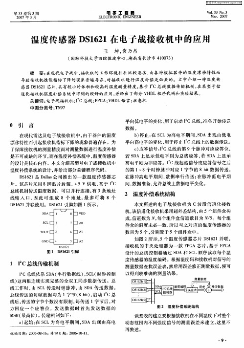
本文所述的电子战接 收机为 c波段信道化接收 机, 该信道化接收机采用超外差结构 , 个组件盒构 由5 成, 信道数为 Ⅳ, 每个组件盒信道数 目为 N 5 / 。每个组 件盒的温度未必一致 , 以与之对应的温度传感器 的 所 数 目为 5个 , 分别 置 于 5个组 件 盒 中。
是不可或缺的环节 , 而在温度补偿系统中, 温度传感器 的设 计是 核心 内容 。本文 介绍某 型 号 电子 战接 收机 中
温度 补偿 系统 的设计 , 给 出部 分关键 程序 代码 。 并
D 12 是 D l s 司推 出的一款 温度传感器 芯 S6 1 aa 公 l 片。该芯 片采用 8脚贴 片封 装 , 供 电, 于 I +5V 基 c 总线机制传送温度数据 。可以并行连接, 3条地址 有 线输 入 V, 此 可 组 成 8个 地 址 , 多 可 将 8个 I因 最 D 12 并 联使用 。D 12 S6 1 S6 1引脚如 图 l 示 。 所
图 2 温度补偿系统结构
误差表 的建 立要 根据接 收机 在不 同温度 下对 整个
动态范围内不同强度信号的测量误差来建立, 这里不
再 赘述 。
・
9・
维普资讯
・
测控技术 ・
电 字 工 曩 师
20 07年 3月
3 1 2 C总线控制 器的 V - L语言描述 I I D
数据 。
在现代雷达及电子战接收机中, 由于器件 的温度 漂移特性而引起接收机指标下降的现象普遍存在。为
了保 障接 收机 的测量 精度 而对 测量数 据进行 温 度补偿
利用DS1620温度传感器构成温度监控系统11
利用DS1620温度传感器构成温度监控系统摘要:为了满足某些环境需要温度测量范围广、温度调节方便等要求,以DS1620温度传感器和单片机为基础,设计了一套温度监控系统。
该系统不仅能够根据环境温度的改变自动调节温度,而且由于DS1620芯片的测量范围广,温度调节方便,使该系统在温度控制、温度测量方面更加精确与方便。
关键词:温度传感器;单片机;监控系统0引言DALLAS公司推出的DS1620是一种具有温度传感、温度控制、温度数据转换等功能的专用集成芯片。
与少量外部单元(如显示、控制器件)结合可构成温度自动测量和控制系统。
测温范围为-55℃~125℃,分辨率为0. 5℃,转换后的温度值采用9位数字量表示。
DS1620可用3线串行接口的方式与单片机相连进行数据的读写操作。
可广泛用于温度控制、温度测量及热敏感系统等领域。
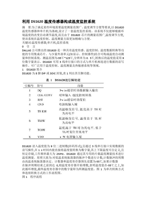
1DS1620简介DS1620为8脚DIP或SOIC封装,表1列出其引脚功能。
DS1620读入温度值为9位二进制数(补码形式),且通过3线串行接口实现数据的读写操作,在1 s时间内能直接将温度值转换为数字量,其上下限温度可自定义,且恒定存储,工作频率最大为2MHz。
DS1620通过其专用的片载温度测量技术进行温度测量。
原理大致为:对低温系统振荡器的脉冲个数进行计数,计数脉冲的周期由高温系统振荡器决定。
计数器和温度寄存器预先设置为-55℃,如果计数器在脉冲周期结束之前到达0,则温度寄存器开始增数,表明温度值在-55℃之上,如此循环增值,最终温度寄存器中的数字量即为所测温度值。
图1为单次转换方式和连续转换方式的工作流程图。
图1程序流程读温度数据(AAH):该指令是读取温度寄存器所存储的最后转换的温度数据,指令输入后的9个移位脉冲将输出寄存器的数据。
写TH(01H):给高温临界寄存器写入TH数据。
指令输入后的9个移位脉冲将9位上限温度值TH写入高温临界寄存器,用来改变THIGH的输出操作。
写TL(02H):给低温临界寄存器写入TL数据。
很有参考价值的数字温度计-1624技术应用
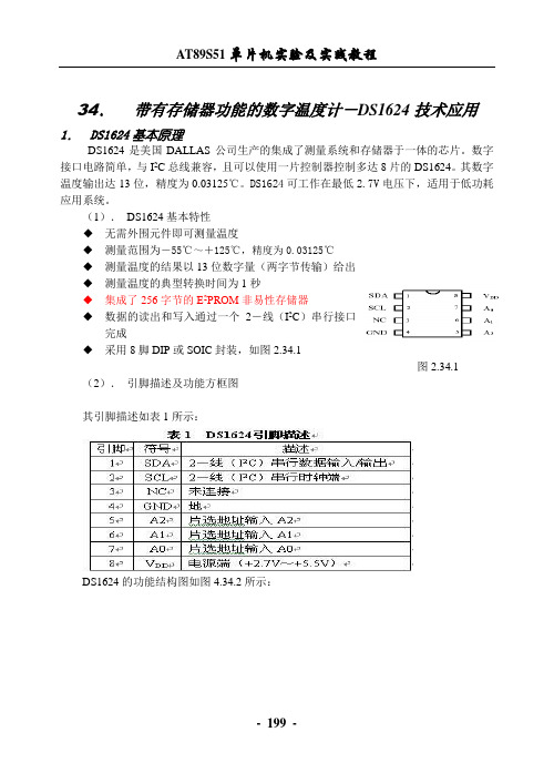
34.带有存储器功能的数字温度计-DS1624技术应用1.DS1624基本原理DS1624是美国DALLAS公司生产的集成了测量系统和存储器于一体的芯片。
数字接口电路简单,与I2C总线兼容,且可以使用一片控制器控制多达8片的DS1624。
其数字温度输出达13位,精度为0.03125℃。
DS1624可工作在最低2.7V电压下,适用于低功耗应用系统。
(1).DS1624基本特性◆无需外围元件即可测量温度◆测量范围为-55℃~+125℃,精度为0.03125℃◆测量温度的结果以13位数字量(两字节传输)给出◆测量温度的典型转换时间为1秒◆集成了256字节的E2PROM非易性存储器◆数据的读出和写入通过一个2-线(I2C)串行接口完成◆采用8脚DIP或SOIC封装,如图2.34.1图2.34.1 (2).引脚描述及功能方框图其引脚描述如表1所示:DS1624的功能结构图如图4.34.2所示:图4.34.2(3).DS1624工作原理温度测量图4.34.3是温度测量的原理结构图图4.34.3温度测量的原理结构图DS1624在测量温度时使用了独有的在线温度测量技术。
它通过在一个由对温度高度敏感的振荡器决定的计数周期内对温度低敏感的振荡器时钟脉冲的计数值的计算来测量温度。
DS1624在计数器中预置了一个初值,它相当于-55℃。
如果计数周期结束之前计数器达到0,已预置了此初值的温度寄存器中的数字就会增加,从而表明温度高于-55℃。
与此同时,计数器斜坡累加电路被重新预置一个值,然后计数器重新对时钟计数,直到计数值为0。
通过改变增加的每1℃内的计数器的计数,斜坡累加电路可以补偿振荡器的非线性误差,以提高精度,任意温度下计数器的值和每一斜坡累加电路的值对应的计数次数须为已知。
DS1624通过这些计算可以得到0.03125℃的精度,温度输出为13位,在发出读温度值请求后还会输出两位补偿值。
表2给出了所测的温度和输出数据的关系。
温度传感器实验报告

温度传感器实验报告
一、实验目的
本实验旨在通过使用温度传感器来检测不同环境下的温度变化,并通过实验数据分析温度传感器的性能和准确度。
二、实验仪器
1. Arduino Uno控制板
2. DS18B20数字温度传感器
3. 杜邦线
4. 电脑
三、实验步骤
1. 连接DS18B20温度传感器到Arduino Uno控制板上。
2. 使用Arduino软件编写读取温度传感器数据的程序。
3. 通过串口监视器读取传感器采集到的温度数据。
4. 将温度传感器放置在不同环境温度下,记录数据并进行分析。
四、实验数据
在室内环境下,温度传感器读取的数据平均值为25摄氏度;在户外阳光下,温度传感器读取的数据平均值为35摄氏度。
五、实验结果分析
通过实验数据分析可知,DS18B20温度传感器对环境温度有较高的
敏感度和准确性,能够较精准地反映环境温度的变化。
在不同环境温
度下,传感器能够稳定地输出准确的温度数据。
六、实验结论
本实验通过对DS18B20温度传感器的测试和分析,验证了其在温
度检测方面的可靠性和准确性。
温度传感器可以广泛应用于各种领域,如气象监测、工业控制等。
通过本次实验,我们对温度传感器的性能
有了更深入的了解。
七、参考文献
1. DS18B20温度传感器数据手册
2. Arduino Uno官方网站
以上为实验报告内容,谢谢!。
实验十二集成电路温度传感器特性测量全解

实验十二集成电路温度传感器特性测量一.概述温度传感器的特性测量和定标是大学普通物理热学实验和电磁学实验中的一个根本内容,是新的全国理工科物理实验教学大纲中一个重要实验。
为开设好此实验,由复旦大学物理实验教学中心和上海复旦天欣科教仪器协作,联合研制了采用DS18B20单线数字温度传感器为测量元件的新一代恒温控制仪。
新仪器与同类其它仪器相比,有以下四个优点:1)传感器体积小;2)控温精度高;3)无污染及噪声(无水银污染且不用继电器);4)设定温度和测量温度均用数字显示。
本实验仪器可用于各种温度传感器的特性测量和各种材料的电阻与温度关系特性测量实验,本仪器也可用于物理化学实验做恒温仪用,它是理工科大学普通物理实验必备重要实验装置之一。
二.用途电流型集成温度传感器AD590的特性测量和应用:(1)测量AD590输出电流和温度的关系,计算传感器灵敏度及0C时传感器输出电流值。
用AD590传感器,电阻箱,数字电压表和直流电源等设计并安装数字式摄氏温度计。
测量集成温度传感器AD590在某恒定温度时的伏安特性曲线,求出AD590线性使用范围的最小电压U r。
三.仪器组成与技术指标1.仪器组成如图1所示,本机为有单片控制的智能式数字恒温控制仪、量程为0-四位半数字电压表、直流稳压输出电源、可调式磁性搅拌器以及2000ml烧杯、加热器、玻璃管〔内放变压器油和被测集成温度传感器〕等组成。
功放89C2051 4位数字显示单片电脑数据译码器控被加温测搅热传传拌器感感器器器DC5V5位数字DC12V电压表—12V恒温水槽直流电机调速DC12 测量输出输入图1技术指标:A.温控仪温度计显示工作温度:0℃-100℃恒温控制温度:室温-80o C(3)控制恒温显示分辨精度:≤±℃直流数字电压表(1)量程:0-(2)读数准确度:量程0.03%±5个字(3)输出电阻:20Ω(为了防止长时间短路内接电阻 )C.温度传感器DS18B20的结构与技术特性〔控温及测温用〕:温度测量范围:-55℃-125℃测温分辨率:℃(1)引脚排列(如图2所示):-2-1〔GND〕:地2〔DQ〕:单线运用的数据输入输出引脚3〔VDD〕:可选的电源引脚图2封装形式:TO-92详细应用请参阅相关资料D.待测温度传感器AD590技术特性:工作温度:—55℃—150℃工作电压:—24V灵敏度:1μA/℃,线性元件(4)0℃时输出电流约273μAE.加热器:工作电压:交流10V—150V工作电流:交流最大.仪器使用方法使用前将电位器调节旋钮逆时针方向旋到底,把接有DS18B20传感器接线端插头插在后面的插座上,DS18B20测温端放入注有少量油的玻璃管内(直径16mm);在2000ml大烧杯内注入1600ml的净水,放入搅拌器和加热器后盖上铝盖并固定。
温度传感器实验报告
一、实验目的1. 了解温度传感器的原理和分类。
2. 掌握温度传感器的应用和特性。
3. 学习温度传感器的安装和调试方法。
4. 通过实验验证温度传感器的测量精度。
二、实验器材1. 温度传感器:DS18B20、热电偶(K型、E型)、热敏电阻(NTC)等。
2. 测量设备:万用表、数据采集器、温度调节器等。
3. 实验平台:温度传感器实验模块、单片机开发板、PC机等。
三、实验原理温度传感器是将温度信号转换为电信号的装置,根据转换原理可分为接触式和非接触式两大类。
本实验主要涉及以下几种温度传感器:1. DS18B20:一款数字温度传感器,具有高精度、高可靠性、易于接口等优点。
2. 热电偶:利用两种不同金属导体的热电效应,将温度信号转换为电信号。
3. 热敏电阻:利用温度变化引起的电阻值变化,将温度信号转换为电信号。
四、实验步骤1. DS18B20温度传感器实验1. 连接DS18B20传感器到单片机开发板。
2. 编写程序读取温度值。
3. 使用数据采集器显示温度值。
4. 验证温度传感器的测量精度。
2. 热电偶温度传感器实验1. 连接热电偶传感器到数据采集器。
2. 调节温度调节器,使热电偶热端温度变化。
3. 使用数据采集器记录热电偶输出电压。
4. 分析热电偶的测温特性。
3. 热敏电阻温度传感器实验1. 连接热敏电阻传感器到单片机开发板。
2. 编写程序读取热敏电阻的电阻值。
3. 使用数据采集器显示温度值。
4. 验证热敏电阻的测温特性。
五、实验结果与分析1. DS18B20温度传感器实验实验结果显示,DS18B20温度传感器的测量精度较高,在±0.5℃范围内。
2. 热电偶温度传感器实验实验结果显示,热电偶的测温特性较好,输出电压与温度呈线性关系。
3. 热敏电阻温度传感器实验实验结果显示,热敏电阻的测温特性较好,电阻值与温度呈非线性关系。
六、实验总结通过本次实验,我们了解了温度传感器的原理和分类,掌握了温度传感器的应用和特性,学会了温度传感器的安装和调试方法。
基于DS1624传感器的温度测试系统的研究
基于DS1624传感器的温度测试系统的研究作者:张宇翔冯锐莉郝向阳来源:《硅谷》2013年第05期摘要本文介绍了利用数字式温度传感器DS1642组成温度测试系统,该测试系统具有组成简单,测试范围广,精度高等,符合温度测试系统的各方面要求,且与计算机接口能为测试提供周期更长的测试。
针对数字温度传感器DS1642的温度滞后性,利用动态补偿方法进行了研究。
关键词温度测试;DS1642;动态补偿中图分类号:TP212 文献标识码:A 文章编号:1671—7597(2013)031-033-02在测试领域,温度传感器的运用越来越广泛,较多使用的有热敏电阻、热电偶、集成式模拟温度传感器等,其特点是测试的温度范围有所区别,测量精度低,且外围电路复杂,测试的结果无法保存,缺乏长时间测试的特点。
DALLAS公司的数字式温度传感器DS1624,其主要功能含有测量功能和存储器功能。
构成测试系统时,与之相连的接口电路简单且外围电路关系明确,与之相连的功能强大的单片机能通过输入输出接口,协调控制与之相连的外围设备,达到测量与控制的作用。
而且加上多片DS1624可以用一个控制器芯片控制。
具有测试系统需求的13位数字温度显示输出,精度可以达到一般温度测试系统要求。
DS1624在最低2.7 V电压之下工作稳定,完全满足在低功耗的温度测试系统中使用。
1 传感器DS1642综合考虑了测量精度、经济性、测温范围、测温系统复杂程度,DS1624温度传感器作为首选。
DS1624的组成只需简单的外部增加合适的电路元器件,就可以满足测试系统需要的功能要求,其优点是该芯片能直接进行片内温度A/D量转化,且具有13位数字量的直接输出,配备合适的元件组成抗干扰能力强的电路,采用2线I2C总线传送接收数据,封装形式为DIP8和SOIC8两种。
DS1624在工作电路中具有独有的在线温度测量功能。
它有一个对温度高度敏感的振荡。
表1给出了所测的温度和输出数据的关系,MSB在前,LSB在后。
分享一个用计算机直接通过串口驱动DS1621测温的温度计
分享一个用计算机直接通过串口驱动DS1621测温的
温度计
今天发现的这个实验作品非常经典,用计算机直接通过串口驱动
DS1621测温,整个测温模块精简之至,没有使用任何单片机和电平转化芯片,涉及的技术还包括串口取电、I2C总线等等。
如果采用单片机驱动DS1621的方案,工作量无异是巨大的,比方说
需要完成计算机跟单片之间的电平转换、以及通讯;需要完成单片机跟
DS1621之间的通讯。
Alberto Ricci Bitti的这个PC实现的温度计,取消了单片机的中转环节,由计算机直接驱动DS1621,省去了单片机部分的大量设计工作,其思路非常犀利,犹如鬼斧神工、别开蹊径。
这种经典的方法只有直接看原理图说话才够爽快。
数字温度传感器DS1621及其应用

DS1621是DALLAS公司生产的一种功能较强的数字式温度传感器和恒温控制器。
与同系列的DS1620相比控制更为简单,接口与I2C总线兼容,且可以使用一片控制器控制多达8片的DS1621。
其数字温度输出达9位,精度为0.5℃。
通过读取内部的计数值和用于温度补偿的每摄氏度计数值,利用公式计算还可提高温度值的精度。
DS1621可工作在最低2.7V 电压下,适用于低功耗应用系统。
利用DS1621和一片2051单片机即可构成一个简洁但功能强大的低电压温度测量控制系统。
1. DS1621基本特性DS1621无需外围元件即可测量温度,将结果以9位数字量(两字节传输)给出,测量范围为-55℃~+155℃,精度为0.5℃;典型转换时间为1s;用户可自行设置恒温计的温度值,且将该设置值存储在非易失存储器中。
数据的读出和写入通过一个2-线串行接口完成,DS1621采用8脚DIP或SOIC封装。
2. 引脚描述及功能方框图DS1621的引脚描述如表1所列。
图1是DS1621的功能框图。
3. DS1621的工作方式DS1621既可独立工作(此时作为恒温控制器),也可通过2-线接口在MPU的控制下完成温度的测量和计算。
DS1621的工作方式是由片上的设置/状态寄存器来决定的,该寄存器的定义如下:其中DONE为转换完成位,温度转换结束时置1,正在进行转换时为0;THF为高温标志位,当温度超过TH预置值时置1;TLF为低温标志位,当温度低于TL预置值时置1;NVB为非易失存储器忙位,向片内E2PROM写入时置1,写入结束后复位写入E2PROM通常需要10ms;PCL为输出极性位,为1时激活状态为逻辑高电平,为0时激活状态为逻辑低电平,该位是非易失的;1SHOT为一次模式位,该位为1时每次收到开始转换命令执行一次温度转换,为0时执行连续温度转换,该位亦是非易失的。
DS1621在嵌入一个系统前,需由MPU将设置/状态寄存器值通过2-线接口写入该寄存器,之后DS1261或作为恒温计独立工作,或在MPU控制下进行温度测量和计算。
24 DS1621温度传感器实验

/*************** writer:shopping.w ******************/ #include <reg52.h>#include <intrins.h>#define uint unsigned int#define uchar unsigned charbit I2C_Busy, NO_Ack,Bus_Fault,point;uchar bdata a;sbit LSB = a^0;sbit MSB = a^7;sbit SDA = P3^3;sbit SCL = P3^2;uchar Array[] = {'0','1','2','3','4','5','6','7','8','9'};uchar command_data[]={0xac,0x00,0xee,0xa1,0x00,0x00,0xa2,0x00,0x00,0xaa};uchar Prompt[]="Waiting for a while...\r";uchar i;void DelayMS(uint ms){uchar i;while(ms--){for(i=0;i<120;i++);}}void SendStop(){SDA = 0;SCL = 1;_nop_();SDA = 1;I2C_Busy = 0;}void SendByte(uchar wd){uchar i;a = wd;for(i=0;i<8;i++){SCL = 0;_nop_();_nop_();SDA = MSB;a <<= 1;_nop_();_nop_();SCL = 1;_nop_();_nop_();SCL = 0;}SDA = 1;SCL = 1;_nop_();_nop_();if(!SDA){SCL = 0;_nop_();_nop_();}else{NO_Ack = 1;SCL = 0;_nop_();_nop_();}}void Master(uchar slave_addr) {I2C_Busy = 1;NO_Ack = 0;Bus_Fault = 0;if(!SCL || !SDA)Bus_Fault = 1;else{SDA = 0;_nop_();_nop_();SCL = 0;_nop_();_nop_();SendByte(slave_addr);}}uchar RecvByte(uchar cnt){uchar i,rcv_data;for(i=0;i<8;i++){SDA = 1;SCL = 1;_nop_();LSB = SDA;if(i<7)a <<= 1;_nop_();SCL = 0;_nop_();}if(cnt == 1)SDA = 1;elseSDA = 0;SCL = 1;_nop_();SCL = 0;SDA = 1;_nop_();rcv_data = a;return rcv_data;}void SendData(uchar slave_address,uchar start,uchar end) {Master(slave_address);for(i=start;i<=end;i++)SendByte(command_data[i]);SendStop();}void InitialiseSerialPort(){TMOD = 0x20;TH1 = 0xfd;SCON = 0x50;TR1 = 1;}void SendCharToSerialPort(uchar ch){SBUF = ch;while(!TI);TI = 0;}void SendTemperatureToSerialPort(uchar val) {if(val>200){val = 255-val;SendCharToSerialPort('-');if(!point)val+=1;}SendCharToSerialPort(Array[(val/10)/10]);SendCharToSerialPort(Array[(val/10)%10]);SendCharToSerialPort(Array[val%10]);SendCharToSerialPort('.');if(point)SendCharToSerialPort('5');elseSendCharToSerialPort('0');SendCharToSerialPort(' ');SendCharToSerialPort('C');SendCharToSerialPort('\r');}void SetTemperatureLimit(uchar HI,uchar LO) {command_data[4] = HI;command_data[5] = 0;command_data[7] = LO;command_data[8] = 0;SendData(0x90,3,5);DelayMS(10);SendData(0x90,6,8);}void StartConversion(){SendData(0x90,2,2);DelayMS(750);}uchar ReadTemp(){uchar d;SendData(0x90,9,9);Master(0x91);d = RecvByte(0);point = RecvByte(1)>>7;SendStop();return d;}void WriteConfig(uchar c){command_data[1] = c;SendData(0x90,0,1);}void main(){uchar i;InitialiseSerialPort();while(Prompt[i]!='\0')SendCharToSerialPort(Prompt[i++]);WriteConfig(0x02);StartConversion();SetTemperatureLimit(40,35);while(1){DelayMS(50);SendTemperatureToSerialPort(ReadTemp());}}。
ds1621温度传感器

FEATURES§ Temperature measurements require no external components § Measures temperatures from –55°C to +125°C in 0.5°C increments. Fahrenheit equivalent is –67°F to 257°F in 0.9°F increments § Temperature is read as a 9–bit value (2-byte transfer)§ Wide power supply range (2.7V to 5.5V)§ Converts temperature to digital word in 1second § Thermostatic settings are user definable and nonvolatile § Data is read from/written via a two–wire serial interface (open drain I/O lines)§ Applications include thermostaticcontrols, industrial systems, consumer products, thermometers, or any thermal sensitive system § 8–pin DIP or SOIC package (150-MIL and 208-MIL)PIN ASSIGNMENTPIN DESCRIPTIONSDA - 2-Wire Serial Data Input/Output SCL - 2-Wire Serial Clock GND - GroundT OUT - Thermostat Output Signal A0- Chip Address Input A1- Chip Address Input A2- Chip Address Input V DD- Power Supply VoltageDESCRIPTIONThe DS1621 Digital Thermometer and Thermostat provides 9–bit temperature readings which indicate the temperature of the device. The thermal alarm output, T OUT , is active when the temperature of the device exceeds a user–defined temperature TH. The output remains active until the temperature drops below user defined temperature TL, allowing for any hysteresis necessary.User-defined temperature settings are stored in nonvolatile memory so parts may be programmed prior to insertion in a system. Temperature settings and temperature readings are all communicated to/from the DS1621 over a simple two–wire serial interface.DS1621Digital Thermometer and ThermostatSDA T OUT GNDV DD A 0A 1A 2DS1621S 8-PIN SOIC (150-MIL)DS1621V 8-PIN SOIC (208-MIL)SDA SCL T OUT GNDV DD A 0A 1A 2DS1621 8-PIN DIP (300-MIL)See Mech Drawings SectionSCLDETAILED PIN DESCRIPTION Table 1PIN SYMBOL DESCRIPTION1SDA Data input/output pin for 2-wire serial communication port.2SCL Clock input/output pin for 2-wire serial communication port.3T OUT Thermostat output. Active when temperature exceeds TH; will reset whentemperature falls below TL.4GND Ground pin.5A2Address input pin.6A1Address input pin.7A0Address input pin.8V DD Supply voltage input power pin. (2.7V – 5.5V)OPERATIONMeasuring TemperatureA block diagram of the DS1621 is shown in Figure 1. The DS1621 measures temperatures through the use of an onboard proprietary temperature measurement technique. A block diagram of the temperature measurement circuitry is shown in Figure 2.The DS1621 measures temperature by counting the number of clock cycles that an oscillator with a low temperature coefficient goes through during a gate period determined by a high temperature coefficient oscillator. The counter is preset with a base count that corresponds to –55°C. If the counter reaches 0 before the gate period is over the temperature register, which is also preset to the –55°C value, is incremented indicating that the temperature is higher than –55°C.At the same time, the counter is preset with a value determined by the slope accumulator circuitry. This circuitry is needed to compensate for the parabolic behavior of the oscillators over temperature. The counter is then clocked again until it reaches 0. If the gate period is still not finished, then this process repeats.The slope accumulator is used to compensate for the nonlinear behavior of the oscillators over temperature, yielding a high resolution temperature measurement. This is done by changing the number of counts necessary for the counter to go through for each incremental degree in temperature. To obtain the desired resolution, both the value of the counter and the number of counts per °C (the value of the slope accumulator) at a given temperature must be known.This calculation is done inside the DS1621 to provide 0.5°C resolution. The temperature reading is provided in a 9–bit, two’s complement reading by issuing the READ TEMPERATURE command. Table 2 describes the exact relationship of output data to measured temperature. The data is transmitted through the 2–wire serial interface, MSB first. The DS1621 can measure temperature over the range of –55°C to +125°C in 0.5°C increments. For Fahrenheit usage a lookup table or conversion factor must be used.DS1621 FUNCTIONAL BLOCK DIAGRAM Figure 1SCLA0A1T OUTTEMPERATURE MEASURING CIRCUITRY Figure 2TEMPERATURE/DATA RELATIONSHIPS Table 2TEMPERATUREDIGITAL OUTPUT(Binary)DIGITAL OUTPUT(Hex)+125°C 01111101 000000007B00h +25°C 00011001 000000001900h +½°C 00000001 000000000080h +0°C 00000000 000000000000h -½°C 11111111 10000000FF80h -25°C 11100111 00000000E700h -55°C11001001 00000000C900hSince data is transmitted over the 2–wire bus MSB first, temperature data may be written to/read from the DS1621 as either a single byte (with temperature resolution of 1°C) or as two bytes. The second byte would contain the value of the least significant (0.5°C) bit of the temperature reading as shown in Table 1. Note that the remaining 7 bits of this byte are set to all "0"s.Temperature is represented in the DS1621 in terms of a ½°C LSB, yielding the following 9–bit format:T = -25°CHigher resolutions may be obtained by reading the temperature and truncating the 0.5°C bit (the LSB)from the read value. This value is TEMP_READ. The value left in the counter may then be read by issuing a READ COUNTER command. This value is the count remaining (COUNT_REMAIN) after the gate period has ceased. By loading the value of the slope accumulator into the count register (using the READ SLOPE command), this value may then be read, yielding the number of counts per degree C (COUNT_PER_C) at that temperature. The actual temperature may be then be calculated by the user using the following:TEMPERATURE=TEMP_READ-0.25 +CPER COUNT REMAIN COUNT C PER COUNT __)___(−Thermostat ControlIn its operating mode, the DS1621 functions as a thermostat with programmable hysteresis as shown in Figure 3. The thermostat output updates as soon as a temperature conversion is complete.When the DS1621’s temperature meets or exceeds the value stored in the high temperature trip register (TH), the output becomes active and will stay active until the temperature falls below the temperature stored in the low temperature trigger register (TL). In this way, any amount of hysteresis may be obtained.The active state for the output is programmable by the user so that an active state may either be a logic "1" (V DD ) or a logic "0" (0V).THERMOSTAT OUTPUT OPERATION Figure 3DQ (Thermostat output, Active=High)OPERATION AND CONTROLThe DS1621 must have temperature settings resident in the TH and TL registers for thermostatic operation. A configuration/status register also determines the method of operation that the DS1621 will use in a particular application, as well as indicating the status of the temperature conversion operation.The configuration register is defined as follows:whereDONE =Conversion Done bit. “1” = Conversion complete, “0” = Conversion in progress.THF=Temperature High Flag. This bit will be set to “1” when the temperature is greater than or equal to the value of TH. It will remain “1” until reset by writing “0” into this location or removing power from the device. This feature provides a method of determining if the DS1621 has ever been subjected to temperatures above TH while power has been applied.TLF=Temperature Low Flag. This bit will be set to “1” when the temperature is less than or equal to the value of TL. It will remain “1” until reset by writing “0” into this location or removing power from the device. This feature provides a method of determining if the DS1621 has ever been subjected to temperatures below TL while power has been applied.NVB=Nonvolatile Memory Busy flag. “1” = Write to an E2memory cell in progress, “0” = nonvolatile memory is not busy. A copy to E2may take up to 10 ms.POL=Output Polarity Bit. “1” = active high, “0” = active low. This bit is nonvolatile.1SHOT=One Shot Mode. If 1SHOT is “1”, the DS1621 will perform one temperature conversion upon receipt of the Start Convert T protocol. If 1SHOT is “0”, the DS1621 will continuously perform temperature conversions. This bit is nonvolatile.For typical thermostat operation the DS1621 will operate in continuous mode. However, for applications where only one reading is needed at certain times or to conserve power, the one–shot mode may be used. Note that the thermostat output (T OUT) will remain in the state it was in after the last valid temperature conversion cycle when operating in one–shot mode.2–WIRE SERIAL DATA BUSThe DS1621 supports a bidirectional 2–wire bus and data transmission protocol. A device that sends data onto the bus is defined as a transmitter, and a device receiving data as a receiver. The device that controls the message is called a “master." The devices that are controlled by the master are “slaves." The bus must be controlled by a master device which generates the serial clock (SCL), controls the bus access, and generates the START and STOP conditions. The DS1621 operates as a slave on the 2–wire bus. Connections to the bus are made via the open–drain I/O lines SDA and SCL.The following bus protocol has been defined (See Figure 4):•Data transfer may be initiated only when the bus is not busy.•During data transfer, the data line must remain stable whenever the clock line is HIGH. Changes in the data line while the clock line is high will be interpreted as control signals.Accordingly, the following bus conditions have been defined:Bus not busy: Both data and clock lines remain HIGH.Start data transfer: A change in the state of the data line, from HIGH to LOW, while the clock is HIGH, defines a START condition.Stop data transfer: A change in the state of the data line, from LOW to HIGH, while the clock line is HIGH, defines the STOP condition.Data valid: The state of the data line represents valid data when, after a START condition, the data line is stable for the duration of the HIGH period of the clock signal. The data on the line must be changed during the LOW period of the clock signal. There is one clock pulse per bit of data.Each data transfer is initiated with a START condition and terminated with a STOP condition. The number of data bytes transferred between START and STOP conditions is not limited and is determined by the master device. The information is transferred byte–wise and each receiver acknowledges with a ninth–bit.Within the bus specifications a regular mode (100 kHz clock rate) and a fast mode (400 kHz clock rate) are defined. The DS1621 works in both modes.Acknowledge: Each receiving device, when addressed, is obliged to generate an acknowledge after the reception of each byte. The master device must generate an extra clock pulse which is associated with this acknowledge bit.A device that acknowledges must pull down the SDA line during the acknowledge clock pulse in such a way that the SDA line is stable LOW during the HIGH period of the acknowledge related clock pulse. Of course, setup and hold times must be taken into account. A master must signal an end of data to the slave by not generating an acknowledge bit on the last byte that has been clocked out of the slave. In this case, the slave must leave the data line HIGH to enable the master to generate the STOP condition.DATA TRANSFER ON 2–WIRE SERIAL BUS Figure 4Figure 4 details how data transfer is accomplished on the 2–wire bus. Depending upon the state of the R/W bit, two types of data transfer are possible:1.Data transfer from a master transmitter to a slave receiver. The first byte transmitted by themaster is the slave address. Next follows a number of data bytes. The slave returns an acknowledge bit after each received byte.2.Data transfer from a slave transmitter to a master receiver. The first byte, the slave address,is transmitted by the master. The slave then returns an acknowledge bit. Next follows a number of data bytes transmitted by the slave to the master. The master returns an acknowledge bit after all received bytes other than the last byte. At the end of the last received byte, a ‘not acknowledge’is returned.The master device generates all of the serial clock pulses and the START and STOP conditions. A transfer is ended with a STOP condition or with a repeated START condition. Since a repeated START condition is also the beginning of the next serial transfer, the bus will not be released.The DS1621 may operate in the following two modes:1.Slave receiver mode: Serial data and clock are received through SDA and SCL. After each byte isreceived an acknowledge bit is transmitted. START and STOP conditions are recognized as the beginning and end of a serial transfer. Address recognition is performed by hardware after reception of the slave address and direction bit.2.Slave transmitter mode: The first byte is received and handled as in the slave receiver mode.However, in this mode the direction bit will indicate that the transfer direction is reversed. Serial data is transmitted on SDA by the DS1621 while the serial clock is input on SCL. START and STOP conditions are recognized as the beginning and end of a serial transfer.SLAVE ADDRESSA control byte is the first byte received following the START condition from the master device. The control byte consists of a 4-bit control code; for the DS1621, this is set as 1001 binary for read and write operations. The next 3 bits of the control byte are the device select bits (A2, A1, A0). They are used by the master device to select which of eight devices are to be accessed. These bits are in effect the 3 least significant bits of the slave address. The last bit of the control byte (R/W) defines the operation to be performed. When set to a “1” a read operation is selected, when set to a “0” a write operation is selected. Following the START condition the DS1621 monitors the SDA bus checking the device type identifier being transmitted. Upon receiving the 1001 code and appropriate device select bits, the slave device outputs an acknowledge signal on the SDA line.2-WIRE SERIAL COMMUNICATION WITH DS1621 Figure 5COMMAND SETData and control information is read from and written to the DS1621 in the format shown in Figure 5. To write to the DS1621, the master will issue the slave address of the DS1621 and the R/W bit will be set to “0”. After receiving an acknowledge, the bus master provides a command protocol. After receiving this protocol, the DS1621 will issue an acknowledge and then the master may send data to the DS1621. If the DS1621 is to be read, the master must send the command protocol as before and then issue a repeated START condition and the control byte again, this time with the R/W bit set to “1” to allow reading of the data from the DS1621. The command set for the DS1621 as shown in Table 3 is as follows:Read Temperature [AAh]This command reads the last temperature conversion result. The DS1621 will send 2 bytes, in the format described earlier, which are the contents of this register.Access TH [A1h]If R/W is “0” this command writes to the TH (HIGH TEMPERATURE) register. After issuing this command, the next 2 bytes written to the DS1621, in the same format as described for reading temperature, will set the high temperature threshold for operation of the T OUT output. If R/W is “1” the value stored in this register is read back.Access TL [A2h]If R/W is “0” this command writes to the TL (LOW TEMPERATURE) register. After issuing this command, the next 2 bytes written to the DS1621, in the same format as described for reading temperature, will set the high temperature threshold for operation of the T OUT output. If R/W is “1” the value stored in this register is read back.Access Config [ACh]If R/W is “0” this command writes to the configuration register. After issuing this command, the next data byte is the value to be written into the configuration register. If R/W is “1” the next data byte read is the value stored in the configuration register.Read Counter [A8h]This command reads the value of the counter byte. This command is valid only if R/W is “1”.Read Slope [A9h]This command reads the value of the slope counter byte from the DS1621. This command is valid only if R/W is “1”.Start Convert T [EEh]This command begins a temperature conversion. No further data is required. In one–shot mode the temperature conversion will be performed and then the DS1621 will remain idle. In continuous mode this command will initiate continuous conversions.Stop Convert T [22h]This command stops temperature conversion. No further data is required. This command may be used to halt a DS1621 in continuous conversion mode. After issuing this command, the current temperaturemeasurement will be completed and the DS1621 will remain idle until a Start Convert T is issued to resume continuous operation.DS1621 COMMAND SET Table 3INSTRUCTION DESCRIPTION PROTOCOL 2-WIRE BUS DATAAFTER ISSUINGPROTOCOL NOTESRead Temperature Read last converted temperaturevalue from temperature register.AAh<read 2 bytes data>Read Counter Reads value of count remainingfrom counter.A8h<read data>Read Slope Reads value of the slopeaccumulator.A9h<read data>Start Convert T Initiates temperatureconversion.EEh idle1 Stop Convert T Halts temperature conversion.22h idle1Access TH Reads or writes hightemperature limit value into THregister.A1h<write data>2Access TL Reads or writes lowtemperature limit value into TLregister.A2h<write data>2Access Config Reads or writes configurationdata to configuration register.ACh<write data>2NOTES:1.In continuous conversion mode a Stop Convert T command will halt continuous conversion. Torestart the Start Convert T command must be issued. In one–shot mode a Start Convert T command must be issued for every temperature reading desired.2.Writing to the E2typically requires 10ms at room temperature. After issuing a write command, nofurther writes should be requested for at least 10 ms.MEMORY FUNCTION EXAMPLEExample: Bus master sets up DS1621 for continuous conversion and thermostatic function.ABSOLUTE MAXIMUM RATINGS*Voltage on Any Pin Relative to Ground–0.5V to +7.0VOperating Temperature–55°C to +125°CStorage Temperature–55°C to +125°CSoldering Temperature260°C for 10 seconds* This is a stress rating only and functional operation of the device at these or any other conditions above those indicated in the operation sections of this specification is not implied. Exposure to absolute maximum rating conditions for extended periods of time may affect reliability. RECOMMENDED DC OPERATING CONDITIONSPARAMETER SYMBOL MIN TYP MAX UNITS NOTES Supply Voltage V DD 2.7 5.5V1DC ELECTRICAL CHARACTERISTICS(-55°C to +125°C; V DD=2.7V to 5.5V) PARAMETER SYMBOL CONDITION MIN TYP MAX UNITS NOTES±½°C Thermometer Error T ERR0°C to 70°C-55°C to + 0°Cand 70°C to 125°C See Typical Curve11Low Level InputVoltageV IL0.50.3 V DD VHigh Level InputVoltageV IH0.7 V DD V DD+0.5VPulse width ofspikes which mustbe suppressed bythe input filtert SP Fast Mode050nsV OL1 3 mA SinkCurrent 00.4VLow Level OutputVoltageV OL2 6 mA SinkCurrent00.6VInput Current eachI/O Pin0.4<V I/O<0.9V DD-1010µA2 I/O Capacitance C I/O10pFActive Supply Current I CCTemperatureConversionE2 WriteCommuni-cation Only1000400100µA3, 4Standby SupplyCurrentI STBY1µA3, 4V OH 1 mA Source 2.4V Thermostat Output(T OUT) OutputVoltageV OL 4 mA Sink0.4VAC ELECTRICAL CHARACTERISTICS (-55°C to +125°C; V DD=2.7V to 5.5V) PARAMETER SYMBOL CONDITION MIN TYP MAX UNITS NOTES TemperatureConversion TimeT TC0.41sNV Write CycleTimet WR0°C to 70°C1050ms10SCL Clock Frequency f SCL Fast ModeStandard Mode400100KHzBus Free Time Between a STOP and START Condition t BUF Fast ModeStandard Mode1.34.7µsHold Time (Repeated) START Condition t HD:STA Fast ModeStandard Mode0.64.0µs5Low Period of SCL Clock T LOW Fast ModeStandard Mode1.34.7µsHigh Period of SCL Clock T HIGH Fast ModeStandard Mode0.64.0µsSetup Time for a Repeated START Condition t SU:STA Fast ModeStandard Mode0.64.7µsData Hold Time t HD:DAT Fast ModeStandard Mode 00.9µs6, 7Data Setup Time t SU:DAT Fast ModeStandard Mode 100250ns8Rise Time of Both SDA and SCL Signals t R Fast ModeStandard Mode20+0.1C B3001000ns9Fall Time of both SDA and SCL Signals t F Fast ModeStandard Mode20+0.1C B300300ns9Setup time for STOP Condition t SU:STO Fast ModeStandard Mode0.64.0µsCapacitative Loadfor each Bus LineC b400pFAll values referred to V IH=0.9 V DD and V IL=0.1 V DD.AC ELECTRICAL CHARACTERISTICS(-55°C to +125°C; VDD=2.7V to 5.5V) PARAMETER SYMBOL MIN TYP MAX UNITS NOTES Input Capacitance C I5pFNOTES:1.All voltages are referenced to ground.2.I/O pins of fast mode devices must not obstruct the SDA and SCL lines if V DD is switched off.3.I CC specified with T OUT pin open.4.I CC specified with V CC at5.0V and SDA, SCL = 5.0V, 0°C to 70°C.5.After this period, the first clock pulse is generated.6. A device must internally provide a hold time of at least 300 ns for the SDA signal (referred to theV IH MIN of the SCL signal) in order to bridge the undefined region of the falling edge of SCL.7.The maximum t HD:DAT has only to be met if the device does not stretch the LOW period (t LOW) of theSCL signal.8. A fast mode device can be used in a standard mode system, but the requirement t SU:DAT >250 ns mustthen be met. This will automatically be the case if the device does not stretch the LOW period of the SCL signal. If such a device does stretch the LOW period of the SCL signal, it must output the next data bit to the SDA line t RMAX+t SU:DAT = 1000+250 = 1250 ns before the SCL line is released.9.C b– total capacitance of one bus line in pF.10.Writing to the nonvolatile memory should only take place in the 0°C to 70°C temperature range.11.See typical curve for specification limits outside 0°C to 70°C range. Thermometer error reflectssensor accuracy as tested during calibration.TIMING DIAGRAMTYPICAL PERFORMANCE CURVEDS1621 DIGITAL THERMOMETER AND THERMOSTATTEMPERATURE READING ERRORTEMPERATURE (deg. C)。
温度传感器实验指导书
温度传感器实验1 实验目的:了解各种温度传感器(热电偶、铂热电阻、PN 结温敏二极管、半导体热敏电阻、集成温度传感器)的测温原理;掌握热电偶的冷端补偿原理; 掌握热电偶的标定过程;了解各种温度传感器的性能特点并比较上述几种传感器的性能。
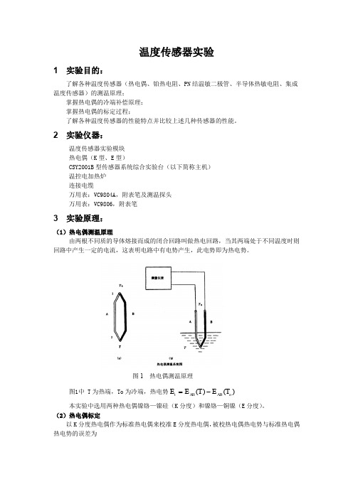
2 实验仪器:温度传感器实验模块 热电偶(K 型、E 型)CSY2001B 型传感器系统综合实验台(以下简称主机) 温控电加热炉 连接电缆万用表:VC9804A ,附表笔及测温探头 万用表:VC9806,附表笔3 实验原理:(1)热电偶测温原理由两根不同质的导体熔接而成的闭合回路叫做热电回路,当其两端处于不同温度时则回路中产生一定的电流,这表明电路中有电势产生,此电势即为热电势。
(图10)图1中 T 为热端,To 为冷端,热电势)()(o AB AB t T E T E E -=本实验中选用两种热电偶镍铬—镍硅(K 分度)和镍铬—铜镍(E 分度)。
(2)热电偶标定以K 分度热电偶作为标准热电偶来校准E 分度热电偶,被校热电偶热电势与标准热电偶热电势的误差为图1 热电偶测温原理校分标标标测标分校测e S S e e e e -⋅-+=∆式中:e 校测——被校热电偶在标定点温度下测得的热电势平均值 e 标测——标准热电偶在标定点温度下测得的热电势平均值 e 标分——标准热电偶分度表上标定温度的热电势值 e 校分——被校热电偶标定温度下分度表上的热电势值。
S 标——标准热电偶的微分热电势 (3)热电偶冷端补偿图2 金属铂热电阻和热敏电阻温度曲线比较(7)集成温度传感器用集成工艺制成的双端电流型温度传感器,在一定的温度范围内按1μA/K的恒定比值输出与温度成正比的电流,通过对电流的测量即可得知温度值(K氏温度),经K氏-摄氏转换电路直接显示℃温度值。
4 实验步骤:(12)根据数据分别绘制K型热电偶和E型热电偶温度与热电势的关系曲线。
(13)将K型热电偶作为标准热电偶,计算被测热电偶E型热电偶的误差。
实验十四温度传感器实验讲述

实验十四温度传感器实验一.实验目的了解数字式温度传感器DS18B20的使用方法。
二.实验原理1.硬件介绍DS18B20是由DALLAS半导体公司推出的一种的“一线总线”接口的温度传感器。
与传统的热敏电阻等测温元件相比,它是一种新型的体积小、适用电压宽、与微处理器接口简单的数字化温度传感器。
一线总线结构具有简洁且经济的特点,可使用户轻松地组建传感器网络,从而为测量系统的构建引入全新概念,测量温度范围为-55~+125℃,精度为±0.5℃。
现场温度直接以“一线总线”的数字方式传输,大大提高了系统的抗干扰性。
它能直接读出被测温度,并且可根据实际要求通过简单的编程实现9~l2位的数字值读数方式。
它工作在3—5.5 V的电压范围。
其内部结构见下图:图1 DS18B20内部结构图ROM中的64位序列号是出厂前被光记好的,它可以看作是该DS18B20的地址序列码,每DS18B20的64位序列号均不相同。
64位ROM的排列是:前8位是产品家族码,接着48位是DS18B20的序列号,最后8位是前面56位的循环冗余校验码(CRC=X8+X5 +X4 +1)。
ROM作用是使每一个DS18B20都各不相同,这样就可实现一根总线上挂接多个。
所有的单总线器件要求采用严格的信号时序,以保证数据的完整性。
DS18B20共有6种信号类型:复位脉冲、应答脉冲、写0、写1、读0和读1。
所有这些信号,除了应答脉冲以外,都由主机发出同步信号。
并且发送所有的命令和数据都是字节的低位在前。
这里我们简单介绍这几个信号的时序:(1)复位脉冲和应答脉冲单总线上的所有通信都是以初始化序列开始。
主机输出低电平,保持低电平时间至少480 us,,以产生复位脉冲。
接着主机释放总线,4.7K的上拉电阻将单总线拉高,延时15~60 us,并进入接收模式(Rx)。
接着DS18B20拉低总线60~240 us,以产生低电平应答脉冲,若为低电平,再延时480 us。
温度传感器测温实验剖析
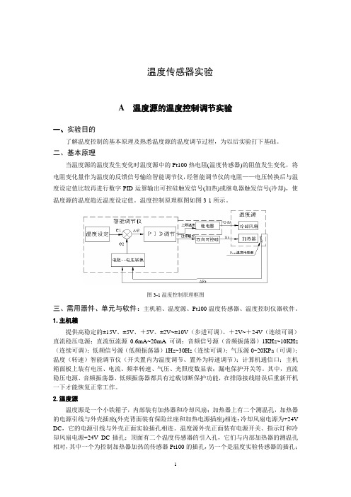
温度传感器实验A 温度源的温度控制调节实验一、实验目的了解温度控制的基本原理及熟悉温度源的温度调节过程,为以后实验打下基础。
二、基本原理当温度源的温度发生变化时温度源中的Pt100热电阻(温度传感器)的阻值发生变化,将电阻变化量作为温度的反馈信号输给智能调节仪,经智能调节仪的电阻——电压转换后与温度设定值比较再进行数字PID运算输出可控硅触发信号(加热)或继电器触发信号(冷却),使温度源的温度趋近温度设定值。
温度控制原理框图如图3-1所示。
图3-1温度控制原理框图三、需用器件、单元与软件:主机箱、温度源、Pt100温度传感器、温度控制仪器软件。
1.主机箱提供高稳定的±15V、±5V、+5V、±2V~±10V(步进可调)、+2V~+24V(连续可调)直流稳压电源;直流恒流源0.6mA~20mA可调;音频信号源(音频振荡器)1KHz~10KHz (连续可调);低频信号源(低频振荡器)1Hz~30Hz(连续可调);气压源0~20KPa(可调);温度(转速)智能调节仪(开关置内为温度调节、置外为转速调节);计算机通信口;主机箱面板上装有电压、电流、频率转速、气压、光照度数显表;漏电保护开关等。
其中,直流稳压电源、音频振荡器、低频振荡器都具有过载切断保护功能,在排除接线错误后重新开机一下才能恢复正常工作。
2.温度源温度源是一个小铁箱子,内部装有加热器和冷却风扇;加热器上有二个测温孔,加热器的电源引线与外壳插座(外壳背面装有保险丝座和加热电源插座)相连;冷却风扇电源为+24V DC,它的电源引线与外壳正面实验插孔相连。
温度源外壳正面装有电源开关、指示灯和冷却风扇电源+24V DC插孔;顶面有二个温度传感器的引入孔,它们与内部加热器的测温孔相对,其中一个为控制加热器加热的传感器Pt100的插孔,另一个是温度实验传感器的插孔;背面有保险丝座和加热器电源插座。
使用时将电源开关打开(O为关,-为开)。
物理实验要求及数据表格实验16温度传感器
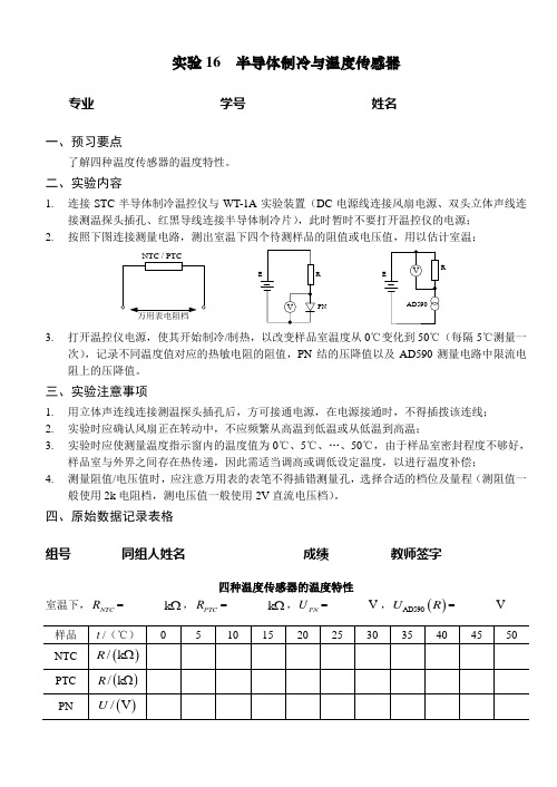
实验16半导体制冷与温度传感器专业___________________学号___________________姓名___________________一、预习要点了解四种温度传感器的温度特性。
二、实验内容1.连接STC半导体制冷温控仪与WT-1A实验装置(DC电源线连接风扇电源、双头立体声线连接测温探头插孔、红黑导线连接半导体制冷片),此时暂时不要打开温控仪的电源;2.按照下图连接测量电路,测出室温下四个待测样品的阻值或电压值,用以估计室温;PN3.打开温控仪电源,使其开始制冷/制热,以改变样品室温度从0℃变化到50℃(每隔5℃测量一次),记录不同温度值对应的热敏电阻的阻值,PN结的压降值以及AD590测量电路中限流电阻上的压降值。
三、实验注意事项1.用立体声连线连接测温探头插孔后,方可接通电源,在电源接通时,不得插拨该连线;2.实验时应确认风扇正在转动中,不应频繁从高温到低温或从低温到高温;3.实验时应使测量温度指示窗内的温度值为0℃、5℃、…、50℃,由于样品室密封程度不够好,样品室与外界之间存在热传递,因此需适当调高或调低设定温度,以进行温度补偿;4.测量阻值/电压值时,应注意万用表的表笔不得插错测量孔,选择合适的档位及量程(测阻值一般使用2k电阻档,测电压值一般使用2V直流电压档)。
四、原始数据记录表格组号________ 同组人姓名____________________ 成绩__________ 教师签字_______________四种温度传感器的温度特性室温下,NTCR=_______kΩ,PTCR=_______kΩ,PNU=_______V,()AD590U R=_______V五、数据处理要求1.用坐标纸画出热敏电阻的阻值与温度的关系图R t-,并用文字表达其温度特性;2.用坐标纸画出PN结两端的压降与温度的关系图U t-,并用文字表达其温度特性;3.通过限流电阻上的压降及其阻值,求出AD590的输出电流,用坐标纸画出电流与温度的关系图I t-,并用文字表达其温度特性。
- 1、下载文档前请自行甄别文档内容的完整性,平台不提供额外的编辑、内容补充、找答案等附加服务。
- 2、"仅部分预览"的文档,不可在线预览部分如存在完整性等问题,可反馈申请退款(可完整预览的文档不适用该条件!)。
- 3、如文档侵犯您的权益,请联系客服反馈,我们会尽快为您处理(人工客服工作时间:9:00-18:30)。
/*************** writer:shopping.w ******************/
#include <reg52.h>
#include <intrins.h>
#define uint unsigned int
#define uchar unsigned char
bit I2C_Busy, NO_Ack,Bus_Fault,point;
uchar bdata a;
sbit LSB = a^0;
sbit MSB = a^7;
sbit SDA = P3^3;
sbit SCL = P3^2;
uchar Array[] = {'0','1','2','3','4','5','6','7','8','9'}; uchar command_data[]=
{
0xac,0x00,0xee,0xa1,0x00,0x00,0xa2,0x00,0x00,0xaa
};
uchar Prompt[]="Waiting for a while...\r";
uchar i;
void DelayMS(uint ms)
{
uchar i;
while(ms--)
{
for(i=0;i<120;i++);
}
}
void SendStop()
{
SDA = 0;
SCL = 1;
_nop_();
SDA = 1;
I2C_Busy = 0;
}
void SendByte(uchar wd)
{
uchar i;
a = wd;
for(i=0;i<8;i++)
{
SCL = 0;
_nop_();
_nop_();
SDA = MSB;
a <<= 1;
_nop_();
_nop_();
SCL = 1;
_nop_();
_nop_();
SCL = 0;
}
SDA = 1;
SCL = 1;
_nop_();
_nop_();
if(!SDA)
{
SCL = 0;
_nop_();
_nop_();
}
else
{
NO_Ack = 1;
SCL = 0;
_nop_();
_nop_();
}
}
void Master(uchar slave_addr) {
I2C_Busy = 1;
NO_Ack = 0;
Bus_Fault = 0;
if(!SCL || !SDA)
Bus_Fault = 1;
else
{
SDA = 0;
_nop_();
_nop_();
SCL = 0;
_nop_();
_nop_();
SendByte(slave_addr);
}
}
uchar RecvByte(uchar cnt)
{
uchar i,rcv_data;
for(i=0;i<8;i++)
{
SDA = 1;
SCL = 1;
_nop_();
LSB = SDA;
if(i<7)
a <<= 1;
_nop_();
SCL = 0;
_nop_();
}
if(cnt == 1)
SDA = 1;
else
SDA = 0;
SCL = 1;
_nop_();
SCL = 0;
SDA = 1;
_nop_();
rcv_data = a;
return rcv_data;
}
void SendData(uchar slave_address,uchar start,uchar end) {
Master(slave_address);
for(i=start;i<=end;i++)
SendByte(command_data[i]);
SendStop();
}
void InitialiseSerialPort()
{
TMOD = 0x20;
TH1 = 0xfd;
SCON = 0x50;
TR1 = 1;
}
void SendCharToSerialPort(uchar ch)
{
SBUF = ch;
while(!TI);
TI = 0;
}
void SendTemperatureToSerialPort(uchar val) {
if(val>200)
{
val = 255-val;
SendCharToSerialPort('-');
if(!point)
val+=1;
}
SendCharToSerialPort(Array[(val/10)/10]);
SendCharToSerialPort(Array[(val/10)%10]);
SendCharToSerialPort(Array[val%10]);
SendCharToSerialPort('.');
if(point)
SendCharToSerialPort('5');
else
SendCharToSerialPort('0');
SendCharToSerialPort(' ');
SendCharToSerialPort('C');
SendCharToSerialPort('\r');
}
void SetTemperatureLimit(uchar HI,uchar LO) {
command_data[4] = HI;
command_data[5] = 0;
command_data[7] = LO;
command_data[8] = 0;
SendData(0x90,3,5);
DelayMS(10);
SendData(0x90,6,8);
}
void StartConversion()
{
SendData(0x90,2,2);
DelayMS(750);
}
uchar ReadTemp()
{
uchar d;
SendData(0x90,9,9);
Master(0x91);
d = RecvByte(0);
point = RecvByte(1)>>7;
SendStop();
return d;
}
void WriteConfig(uchar c)
{
command_data[1] = c;
SendData(0x90,0,1);
}
void main()
{
uchar i;
InitialiseSerialPort();
while(Prompt[i]!='\0')
SendCharToSerialPort(Prompt[i++]);
WriteConfig(0x02);
StartConversion();
SetTemperatureLimit(40,35);
while(1)
{
DelayMS(50);
SendTemperatureToSerialPort(ReadTemp());
}
}。