移位寄存器
移位寄存器原理

移位寄存器原理引言移位寄存器是一种常见的数字电路元件,它用于在计算机和其他数字系统中处理串行数据的移位操作。
本文将介绍移位寄存器的原理和工作方式。
移位寄存器的定义移位寄存器是一种特殊的存储器元件,它可以在输入端和输出端之间进行数据移位操作。
移位寄存器通常是由触发器组成的,每个触发器都可以存储一个位(bit)的数据。
移位寄存器的输入端和输出端都是并行接口,但是数据在寄存器内部是以串行的方式传输的。
移位寄存器的工作原理并行加载移位寄存器最常见的操作之一是并行加载。
在这种操作模式下,通过并行输入引脚将数据加载到移位寄存器中。
当时钟信号到达时,移位寄存器将存储的数据向左或向右移位,并将其输出到并行输出引脚。
移位的方向由控制信号决定。
串行移位除了并行加载,移位寄存器还可以进行串行移位操作。
在串行移位模式下,输入数据通过串行输入引脚进入移位寄存器,并且顺序地从寄存器的一端移出。
当时钟信号到达时,移位寄存器会将存储的数据按位移动一个位置,并从另一端输出。
这种操作模式可以用于各种应用,例如数据的平移、数据的旋转等。
循环移位循环移位是移位寄存器的另一个重要特性。
在循环移位模式下,移位寄存器的输出会通过反馈引脚重新进入输入端,形成一个闭环。
当时钟信号到达时,移位寄存器将在输入和输出之间循环移动数据。
这种操作模式常用于数据的循环处理、数据的延时等应用场景。
移位寄存器的应用移位寄存器在数字系统中有广泛的应用。
以下是一些常见的应用场景:•移位寄存器常用于串行通信中的数据传输和接收。
通过移位寄存器,可以将并行数据转换为串行数据进行传输,并将接收到的串行数据重新转换为并行数据。
•移位寄存器可以用于数字时钟电路中。
通过串行输入信号和移位寄存器的移位操作,可以实现时钟信号的频率除法,从而生成不同的时钟信号。
•移位寄存器还可用于数据的处理和分析。
例如,在图像处理中,移位寄存器可以用来进行图像平移、旋转和缩放等操作。
总结移位寄存器是一种常见的数字电路元件,用于处理串行数据的移位操作。
移位寄存器实验报告结果

一、实验目的本次实验的主要目的是通过搭建移位寄存器实验电路,验证移位寄存器的逻辑功能,并了解其在数字系统中的应用。
实验内容包括:移位寄存器的基本原理、实验电路搭建、实验现象观察和结果分析。
二、实验原理移位寄存器是一种具有移位功能的寄存器,它可以实现数据的串行输入和串行输出。
在时钟脉冲的作用下,移位寄存器中的数据可以依次左移或右移。
根据移位寄存器存取信息的方式不同,可分为串入串出、串入并出、并入串出、并入并出四种形式。
本实验选用的是4位双向通用移位寄存器,型号为74LS194或CC40194。
74LS194具有5种不同操作模式:即并行送数寄存、右移、左移、保持及清零。
其逻辑符号及引脚排列如图1所示。
图1 74LS194的逻辑符号及其引脚排列三、实验电路搭建1. 电路元件准备:74LS194芯片、电阻、电容、二极管、连接线等。
2. 电路搭建:按照图1所示,将74LS194芯片的引脚与电阻、电容、二极管等元件连接,形成移位寄存器实验电路。
3. 电源连接:将电源正负极分别连接到电路板上的VCC和GND端。
四、实验现象观察1. 实验现象一:串行输入,并行输出。
(1)将74LS194的SR端接地,SL端接高电平,S1、S0端接高电平,CR端接地。
(2)使用串行输入端输入数据,观察并行输出端的数据变化。
(3)实验现象:当输入串行数据时,并行输出端依次输出对应的数据。
2. 实验现象二:并行输入,串行输出。
(1)将74LS194的SR端接地,SL端接高电平,S1、S0端接低电平,CR端接地。
(2)使用并行输入端输入数据,观察串行输出端的数据变化。
(3)实验现象:当输入并行数据时,串行输出端依次输出对应的数据。
3. 实验现象三:左移、右移操作。
(1)将74LS194的SR端接地,SL端接高电平,S1、S0端分别接高电平和低电平,CR端接地。
(2)观察移位寄存器中的数据在时钟脉冲的作用下左移或右移。
(3)实验现象:在时钟脉冲的作用下,移位寄存器中的数据依次左移或右移。
什么是电路中的移位寄存器
什么是电路中的移位寄存器电路中的移位寄存器是一种重要的数字电路元件,用于在计算机与数字系统中实现数据存储、传输和处理的功能。
它能够以特定的方式存储和移动数据位,以满足不同的应用需求。
本文将介绍移位寄存器的定义、工作原理、分类以及应用领域,以及对于这些内容的深入讨论。
一、定义移位寄存器是一种能够保存、移动和处理二进制数据的电路元件。
它可以在时钟信号的控制下,将数据位从一个位置移动到另一个位置,实现数据的传输和存储。
移位寄存器通常由触发器、逻辑门和控制电路组成。
二、工作原理移位寄存器的工作原理基于触发器的特性,触发器是一种能够存储一个位信息的电路元件。
在移位寄存器中,触发器被连接成一个环状结构,形成一个寄存器单元。
时钟信号的上升沿或下降沿触发触发器的工作,使得数据位可以在触发器之间传输。
三、分类根据数据的传输方式,移位寄存器可以分为以下几种类型:串行输入/串行输出(SISO)寄存器、并行输入/串行输出(PISO)寄存器、串行输入/并行输出(SIPO)寄存器、并行输入/并行输出(PIPO)寄存器。
不同类型的移位寄存器适用于不同的应用情况。
1. 串行输入/串行输出(SISO)寄存器:每个时钟周期只能输入或输出一个数据位。
适用于需要一位一位地进行数据处理的应用,如二进制计数器。
2. 并行输入/串行输出(PISO)寄存器:能够一次性输入多个数据位,但每个时钟周期只能输出一个数据位。
适用于需要将并行数据串行输出的应用,如帧同步。
3. 串行输入/并行输出(SIPO)寄存器:每个时钟周期只能输入一个数据位,但可以一次性输出多个数据位。
适用于需要从串行数据中提取并行数据的应用,如数据解码。
4. 并行输入/并行输出(PIPO)寄存器:能够一次性输入和输出多个数据位。
适用于需要同时处理并行数据的应用,如数字滤波器。
四、应用领域移位寄存器在数字电路中有广泛的应用,以下是一些常见的应用领域:1. 数据存储:移位寄存器可以用于保存计算机或数字系统中的数据。
移位寄存器工作原理

移位寄存器工作原理
移位寄存器是一种在数字电路中常用的重要元件,它可以将二进制数据按照一定的规律进行移位操作。
其工作原理如下:
1. 移位寄存器由多个触发器组成,常见的有D触发器、JK触
发器等。
每个触发器都可以存储一个二进制位。
2. 顺序移位寄存器中,触发器按照一定的顺序连接起来,每个触发器的输出接到下一个触发器的输入。
3. 并行移位寄存器中,所有的触发器的时钟信号都是相同的,即它们同时进行状态的更新。
4. 当时钟信号到达时,触发器按照一定的规则将输入数据传递给下一个触发器,并将上一个触发器的输出传递给自己的输出。
5. 移位操作可以是向左移位或向右移位,这取决于触发器的连接方式。
向左移位表示数据向高位移动,而向右移位表示数据向低位移动。
6. 移位寄存器还可以通过加载操作将特定的数据加载到触发器中,实现对寄存器的初始化或重置。
7. 移位寄存器常用于数据传输、数据序列生成、数字信号处理等领域,可以实现数据的移位、平移、循环移位等功能。
总之,移位寄存器的工作原理是利用触发器的连接方式和时钟
信号的控制,实现对二进制数据的移位操作。
它在数字电路中有着广泛的应用,是实现许多逻辑和运算功能的重要组成部分。
移位寄存器的工作原理
移位寄存器的工作原理
移位寄存器是一种常用的数字逻辑电路,用于将输入数据在寄存器内部进行移动。
其工作原理如下:
1. 轮流传递数据:移位寄存器由一系列锁存器组成,每个锁存器都可以存储一个位(二进制数的一位)。
在工作时,输入数据按照一定的顺序被输入到第一个锁存器中,然后通过时钟信号的触发,每个锁存器上的数据都会向下一个锁存器传递。
这样,数据就会像一个“串”一样在寄存器内部传递下去。
2. 移动方向:移位寄存器有两种不同的移动方向:左移和右移。
在左移操作中,输入数据从右边的锁存器向左边的锁存器移动;而在右移操作中,输入数据从左边的锁存器向右边的锁存器移动。
3. 清除和装载:移位寄存器还可以通过清除或装载操作来改变寄存器的内容。
清除操作会将所有锁存器中的数据清零,而装载操作则会将输入的数据重新加载到寄存器中。
4. 并行输入/输出:移位寄存器通常还具有并行输入和并行输
出功能。
这意味着可以同时输入一组数据到寄存器中,或者同时输出一组数据从寄存器中读取。
通过合理地控制时钟信号和输入控制信号,移位寄存器可以实现数据的移位、清除和装载等功能。
在数字电路和计算机体系结构中,移位寄存器被广泛应用于数据处理、通信和控制等领域。
移位寄存器
移位寄存器移位是指在移位脉冲控制下,触发器的状态向左或向右依次转移的数码处理方式。
移位寄存器不仅能寄存数码,还具有移位功能。
移位寄存器由哪些部分组成?它是如何工作的?一、电路组成4个JK触发器+非门各个触发器只具有置0、置1功能。
移位控制信号同时加到各触发器的CP端。
JK触发器构成的4位单向右移寄存器二、工作过程00001 0 1 11FF0 FF1 FF2 FF3清0CP 110001000 JK 触发器构成的4位单向右移寄存器0串行输入D 3D 2D 1D 0串行输入二、工作过程00001 0 1 1清0CP 1100010000100 JK 触发器构成的4位单向右移寄存器串行输入D 3D 2D 1D 0CP 2001FF0 FF1 FF2 FF3串行输入二、工作过程00001 0 1 1清0CP 11000000100 JK 触发器构成的4位单向右移寄存器串行输入D 3D 2D 1D 0CP 2011010CP 31101FF0 FF1 FF2 FF3串行输入二、工作过程00001 0 1 1清0CP 1100000100 JK 触发器构成的4位单向右移寄存器串行输入D 3D 2D 1D 0CP 21010CP 3101CP 411101101 在CP 下降沿作用下,待存数码送到FF0,其他各触发器的状态与CP 作用前一瞬间低1位触发器的状态相同,即寄存器中的原有数码依次右移1位。
FF0 FF1 FF2 FF3串行输入并行输出串行输入串行输出JK触发器构成的4位单向右移寄存器当外部需要该组数码时,可从Q3 ~ Q0并行输出,也可再经4次移位将数码从Q3 端逐位输出,即串行输出。
除了右移寄存器外,还有左移寄存器。
既可左移,也可右移。
三、集成双向移位寄存器(a )实物(b )引脚排列并行数据输入端右移串行数据输入端左移串行数据输入端并行数据输出端操作模式控制端时钟脉冲输入端直接清零端74LS194集成双向移位寄存器74LS194逻辑功能表移位寄存器一、电路组成二、工作过程在CP下降沿作用下,寄存器中的原有数码依次右移1位。
移位寄存器讲解
移位寄存器讲解移位寄存器是一种常见的数字电路,它可以将输入数据进行移位操作,并将结果输出。
移位寄存器通常由多个触发器组成,每个触发器都可以存储一个二进制位。
通过控制触发器的时钟信号和输入数据的传输,移位寄存器可以实现不同的移位操作。
移位寄存器的应用非常广泛,例如在串行通信中,可以使用移位寄存器将并行数据转换为串行数据进行传输;在数字信号处理中,可以使用移位寄存器实现数字滤波器、数字乘法器等功能;在计算机系统中,可以使用移位寄存器实现移位运算、逻辑运算等操作。
移位寄存器的基本操作包括移位、清零和加载。
移位操作可以将寄存器中的数据向左或向右移动一定的位数,移位的方式可以是逻辑移位或算术移位。
逻辑移位是指在移位过程中,保持最高位不变,最低位填充0或1;算术移位是指在移位过程中,保持符号位不变,最低位填充0或1。
清零操作可以将寄存器中的所有位都清零,加载操作可以将输入数据加载到寄存器中。
移位寄存器的实现方式有多种,其中最常见的是串行移位寄存器和并行移位寄存器。
串行移位寄存器是由多个触发器组成的,每个触发器都与相邻的触发器串联,形成一个环形结构。
输入数据从一个触发器进入,经过多次移位后,最终输出到另一个触发器中。
并行移位寄存器是由多个触发器组成的,每个触发器都可以独立地存储一个二进制位。
输入数据可以同时进入多个触发器中,经过多次移位后,最终输出到多个触发器中。
移位寄存器的性能指标包括移位速度、存储容量和功耗等。
移位速度是指寄存器进行移位操作的速度,通常以时钟周期数或移位速率来衡量。
存储容量是指寄存器可以存储的二进制位数,通常以比特数来表示。
功耗是指寄存器在工作过程中消耗的电能,通常以功率或能量来衡量。
移位寄存器是一种非常重要的数字电路,它可以实现多种移位操作,并广泛应用于通信、信号处理、计算机系统等领域。
在设计移位寄存器时,需要考虑多种因素,如性能、功耗、可靠性等,以满足不同应用的需求。
移位寄存器的设计及实现
移位寄存器的设计及实现移位寄存器(Shift Register)是一种常用的数字逻辑电路器件,它能够将数据按照输入和输出的时序进行移位操作。
通过移位寄存器,我们可以实现数据的串行传输、并行-串行或者串行-并行转换、数据延迟等功能。
本文将对移位寄存器的设计与实现进行介绍。
一、移位寄存器的设计1.串行输入、串行输出的移位寄存器这种移位寄存器称为串行移位寄存器,它包括n个触发器,每个触发器提供一个数据位的存储空间。
数据通过一个输入端串行输入,然后通过触发器依次移位,最后从输出端串行输出。
2.并行输入、并行输出的移位寄存器这种移位寄存器称为并行移位寄存器,它包括n个触发器,每个触发器提供一个数据位的存储空间。
数据通过n个输入端并行输入到各个触发器,然后通过控制信号进行同步移位。
最后从n个输出端并行输出。
3.并行输入、串行输出的移位寄存器这种移位寄存器称为并行-串行移位寄存器,它先从n个输入端并行输入数据,然后通过控制信号进行同步移位,并将移位结果通过一个输出端串行输出。
4.串行输入、并行输出的移位寄存器这种移位寄存器称为串行-并行移位寄存器,它先从一个输入端串行输入数据,然后通过触发器进行移位,最后将移位结果从n个输出端并行输出。
1.触发器选择由于是8位移位寄存器,需要选择8个触发器。
常用的触发器有D触发器、JK触发器等,可以根据实际需求选择合适的触发器。
2.输入输出端口设计设计一个输入端口用于串行输入数据。
由于是串行输入,需要一个时钟信号和一个使能信号进行同步移位操作。
同时,设计一个输出端口用于串行输出数据。
3.控制信号电路设计根据串行输入、串行输出的要求,需要设计一个时钟信号和一个使能信号的电路。
使能信号在移位过程中保持逻辑高电平,只有当8位数据全部移位完成时才将使能信号置为逻辑低电平。
二、移位寄存器的实现1.设计一个8位移位寄存器电路,并连接8个D触发器。
2.将串行输入信号与D触发器的数据端相连,时钟信号与D触发器的时钟端相连,使能信号与D触发器的使能端相连。
《移位寄存器》课件

技术挑战与展望
高精度与高稳定性
随着应用需求的不断升级,对移位寄存器的精度和稳定性要求也越来越高。未来的研究将 致力于提高移位寄存器的性能指标,以满足各种高端应用的需求。
低功耗与高能效
在便携式和移动设备中,功耗和能效是至关重要的性能指标。未来的移位寄存器设计将更 加注重节能和能效提升,以延长设备的续航时间和降低运行成本。
硬件描述语言实现
使用Verilog或VHDL等硬件描述语言编写移位寄存器的逻辑 电路,通过仿真和综合工具生成可编程逻辑门阵列(FPGA) 或专用集成电路(ASIC)的配置文件。
集成电路实现
将移位寄存器的逻辑电路直接集成在一片集成电路(IC)中 ,通过外部接口与其它电路或系统连接。
基于软件的实现方式
ASIC实现
将移位寄存器的逻辑电路定制集成到专用集成电路(ASIC)中,通过硬件实现移位寄 存器的功能。ASIC具有高性能和低功耗的特点,但开发周期较长且成本较高。
05 移位寄存器的性能指标与 优化
性能指标
吞吐量
衡量移位寄存器处理数据的能 力,通常以每秒传输的位数( bps)或每秒传输的帧数(fps
。
02
小型化
随着便携式电子设备的普及,移位寄存器的小型化需求也越来越迫切。
小型化移位寄存器的设计需要综合考虑性能、功耗和集成度等多个因素
。
03
智能化
智能化是当前电子设备的重要发展方向,移位寄存器也不例外。通过集
成智能算法和传感器,移位寄存器可以实现自适应控制和预测性维护等
功能,提高设备的整体性能和可靠性。
集成化与模块化
集成化和模块化是提高移位寄存器可靠性和可维护性的重要手段。未来的移位寄存器将更 加注重模块化和可扩展性设计,以方便设备的组装和维护。同时,集成化设计也有助于减 小设备体积和重量,满足便携式应用的需求。
数字电路与逻辑设计2寄存器移位寄存器

并行读出脉冲必须在经过5个移存脉冲后出 现,而且和移存脉冲出现旳时间错开。
D5
D4
D3
D2
D1
&
&
&
&
&
并行读出指令
串行输 入 1D
11001
CI
1D Q1
CI
1D Q2
CI
1D Q3
CI
1D
Q4
Q5
CI
移存脉冲CP
分析:假设串行输入旳数码为10011(左边先入)
串—并行转换状态表
序号 Q1 Q2 Q3 Q4 Q5
工作过程: ①在开启脉冲和时钟CP作用下,执行并
行置入功能。片ⅡQ3=DI6。 ②开启脉冲消失,在CP作用下,因为标志位0
旳存在,使门G1输出为1,使得SH/LD =1,执行右移移位寄存功能。 ③后来在移存脉冲作用,并行输入数据由片Ⅱ旳 Q3逐位串行输出,同步又不断地将片Ⅰ旳串 行输入端J,K=1旳数据移位寄存到寄存器。
末级输出反相后,接到串行输入端。
Q3Q2Q1Q0
1
0000
0001
0011
0111
∧
Q0Q 1Q2Q 3
CP D SR
74194
S0
1
S1
0
RD D 0 D 1 D2 D 3 D SL
1000
1100
1110
1111
0010
0101
1011
0110
清零
1001 0100
1010
1101
移位寄存器构成旳移位计数器
异步清零 同步置数
高位向低位移动(左移) 低位向高位移动(右移)
保持
3 、用集成移位寄存器实现任意模值 旳计数分频
3_移位寄存器_部分

清0),所以Rd端称为复位端.在触发器工作时,Rd应接来高输电出平什1.
么状态。
作用 举例
Q3
Q2
Q1
Q0
CP
FF3
FF2
FF1
FF0
QC
QC
QC
QC
D
QD
QD
QD
QD
0
0
0
0
0
Rd
本继页续完
Rd移置位0工寄作存过器程
一、移位寄存器的工作原理
1、四位左移寄存器逻辑电路图
电路特点:由四个D触发器串联而成,时钟脉冲同时与四个 D 触
CD1
1
CP
Rd
本继页续完
Q3
10 FF3
QC
Q
D
1
0
Q2
Q1
Q0
101 FF2
11 FF1
110 FF0
Q第C三个CP上Q升C沿到达移Q位C0
QD
11
Q D1 1
QD
1
CP
01
Rd
本继页续完
移位寄寄存存器器关闭
一、移位寄存器的工作原理 1、四位左移寄存器逻辑电路图 2、四位左移寄存器工作原理 以在D端输入D3D2D1D0=1101为例,数据从高位开始输入,经历四 个CP脉冲上升沿后全部输入左移寄存器.(分析时一定要运用好每 一个 D 触发器的输出是后一级的输入这个重要的特征.)
一个 D 触发器的输出是后一级的输入这个重要的特征.)
所有触
发器关门
Q3
0 FF3
QC
Q
D
1
0
Q2
0 FF2
QC
Q
D
1
单片机移位寄存器

单片机移位寄存器引言:在单片机的应用中,移位寄存器是一种非常常用的功能模块。
它能够实现数据的移位操作,常被用于串行通信、显示控制、数据传输等场景。
本文将介绍移位寄存器的工作原理、应用领域以及设计注意事项。
一、移位寄存器的工作原理移位寄存器是一种能够将数据按位进行移位操作的寄存器。
它内部由多个触发器组成,每个触发器都能存储一个二进制位。
移位寄存器的输入端可以接收一个数据位,通过控制线来选择是向左移位还是向右移位。
当移位方向选择为向左移位时,寄存器中的所有数据位都向左移动一位,最右边的数据位被丢弃,同时在最左边补入一个新的数据位。
当移位方向选择为向右移位时,寄存器中的所有数据位都向右移动一位,最左边的数据位被丢弃,同时在最右边补入一个新的数据位。
这样就实现了数据的移位操作。
二、移位寄存器的应用领域1. 串行通信:移位寄存器常被用于串行通信中,它可以将并行数据转换为串行数据进行传输。
通过不断地向右移位,将并行数据逐位发送出去,从而实现数据的串行传输。
在接收端,再通过向左移位将串行数据转换为并行数据进行处理。
2. 显示控制:在数码管显示、液晶显示等场景中,移位寄存器可以用来控制显示的内容。
将需要显示的数据按照一定的格式存储在移位寄存器中,然后通过移位操作将数据逐位输出到显示模块,实现显示效果。
3. 数据传输:移位寄存器还可以用于数据传输场景。
例如,将传感器采集到的数据存储在移位寄存器中,通过移位操作将数据传输到其他模块进行处理或存储。
三、移位寄存器的设计注意事项1. 移位方向的选择:在设计中需要明确移位的方向,根据实际需求选择向左移位还是向右移位。
2. 移位速度的控制:移位的速度需要根据具体应用场景进行控制,过快或过慢都可能导致数据错误。
3. 寄存器位数的选择:根据需要存储的数据位数选择合适的移位寄存器。
位数过少可能导致数据丢失,位数过多则会浪费资源。
4. 级联的设计:如果需要存储的数据位数超过一个移位寄存器所能存储的范围,可以通过级联多个移位寄存器来实现,需要合理设计级联的方式和控制信号。
单片机移位寄存器

单片机移位寄存器在单片机中,移位寄存器是一种重要的功能模块,用于实现数据的移位操作。
移位寄存器通过改变数据的位序,可以实现数据在寄存器内部的移动和重排。
它在数字电路和信号处理中具有广泛的应用,如数据压缩、图像处理、通信等领域。
1. 移位寄存器的基本概念移位寄存器是一种特殊的寄存器,它具有多个存储单元(位),每个存储单元可以存储一个二进制位。
移位寄存器可以实现数据的左移和右移操作,通过改变数据的位置,可以将数据位重新排列。
移位寄存器可以分为串行移位寄存器和并行移位寄存器两种类型。
2. 串行移位寄存器串行移位寄存器是由多个触发器级联而成的,数据在寄存器内部逐个位地移动。
通常情况下,串行移位寄存器有一个输入端和一个输出端,数据通过输入端进入寄存器,经过一系列的触发器后,从输出端输出。
串行移位寄存器具有较小的尺寸和较低的功耗,适用于复杂的移位操作。
3. 并行移位寄存器并行移位寄存器是由多个存储单元并列连接而成的,数据同时在所有存储单元内进行移动。
并行移位寄存器具有较高的并行性和处理速度,但尺寸较大且功耗较高。
并行移位寄存器适合于对数据进行快速处理和重排。
4. 移位寄存器的应用移位寄存器在数字电路和信号处理中有广泛的应用。
在数字电路中,移位寄存器用于实现数据的序列操作,如数据的移动、重排、加密等。
在信号处理中,移位寄存器用于数据的滤波、压缩、编码/解码等操作。
5. 移位寄存器的扩展移位寄存器可以通过级联或并行连接的方式进行扩展。
级联连接是通过将多个移位寄存器的输出端与下一个移位寄存器的输入端相连,形成一个更大的移位寄存器。
并行连接是通过将多个移位寄存器的输入端同时连接到数据源,以实现更高的处理速度和并行性。
6. 总结移位寄存器作为一种重要的功能模块,在单片机中具有广泛的应用。
它可以实现数据的移位操作,改变数据的位序,从而实现数据的移动和重排。
串行移位寄存器和并行移位寄存器是常见的两种类型,各有优缺点。
移位寄存器可以通过级联或并行连接进行扩展,以满足不同场景的需求。
移位寄存器

移位寄存器寄存器在数字电路中,用来存放二进制数据或代码的电路称为寄存器。
寄存器是由具有存储功能的触发器组合起来构成的。
一个触发器可以存储一位二进制代码,存放N位二进制代码的寄存器,需用n个触发器来构成。
按功能可分为:基本寄存器和移位寄存器。
移位寄存器移位寄存器中的数据可以在移位脉冲作用下一次逐位右移或左移,数据既可以并行输入、并行输出,也可以串行输入、串行输出,还可以并行输入、串行输出,串行输入、并行输出,十分灵活,用途也很广。
目前常用的集成移位寄存器种类很多,如74164、74165、74166均为八位单向移位寄存器,74195为四位单向移存器,74194为四位双向移存器,74198为八位双向移存器。
反馈移位寄存器(一)、反馈移位寄存器的介绍1. 什么是反馈移位寄存器ai表示二值(0,1)存储单元,ai的个数n成为反馈移位寄存器的级。
在某一时刻,这些级构成该反馈移位寄存器的一个状态,共有2n个可能状态,每一个状态对应于域GF(2)上的一个n维向量,用(a1,a2,a3,…an)表示。
在主时钟周期的周期区间上,每一级存储器ai都将内容向下一级ai-1传递,并根据寄存器的当前状态f(a1,a2,a3,…an)作为an的下一时间内容,即从一个状态转移到下一个状态。
其中函数f(a1,a2,a3,…an)称为该反馈移位寄存器的反馈函数。
2. 线性反馈移位寄存器和非线性反馈移位寄存器如果反馈函数f(a1,a2,a3,…an)是a1,a2,a3,…an 的线性函数函数,则该反馈移位寄存器是线性反馈移位寄存器用LFSR表示,比如:f(a1,a2,a3,…an)=kna1⊕kn-1a2⊕….⊕k2an-1⊕k1an,其中系数ki∈{0,1}(i=1,2,3,…,n)。
相应的如果反馈函数f(a1,a2,a3,…an)是a1,a2,a3,…an 的非线性函数函数,则该反馈移位寄存器是非线性反馈移位寄存器。
(二)、反馈移位寄存器的性质1.移位寄存器序列反馈函数f(a1,a2,a3,…an)为n元布尔函数。
寄存器和移位寄存器
Q0 Q1 Q2 Q3 CO
计数器
74LS138
STA
Y0
STB
Y1
STC
Y2
Y3
Y4
Y5
Y6
Y7
译码器
Y0 Y1 Y2 Y3 Y4 Y5 Y6 Y7
EXIT
本章小结
时序逻辑电路由触发器和组合逻辑电路构成, 其中触发器必不可少。时序逻辑电路旳输出 不但与输入有关,而且还与电路原来旳状态 有关。时序逻辑电路旳工作状态由触发器存 储和表达。
二、移位寄存器
Shift register 用于存储数码和使数码根据需要向左或向右移位。
单向移位 寄存器
左移 寄存器
右移 寄存器
每输入一种移位脉冲,移位寄存器 中旳数码依次向左移动 1 位。
每输入一种移位脉冲,移位寄存器 中旳数码依次向右移动 1 位。
双向移位 寄存器
在控制信号作用下,可实现右移 也可实现左移。
中规模集成计数器功能完善、使用以便灵活。 功能表是其正确使用旳根据。利用中规模集成 计数器可很以便地构成 N 进制(任意进制)计 数器。其主要措施为:
(1) 用同步置零端或置数端取得 N 进制计 数器。这时应根据 SN-1 相应旳二进制代码写 反馈函数。
(2) 用异步置零端或置数端取得 N 进制计 数器。这时应根据 SN 相应旳二进制代码写反 馈函数。
旳状态不变下,面即请寄看存置旳数数演码示保持不变。
寄存器旳构造特点
Q0 Q0
FF0 1D C1 R
Q1 Q1
FF1 1D C1 R
Q2 Q2
FF2 1D C1 R源自Q3 Q3FF3 1D C1 R
D0 CP CR D1
移位寄存器讲解
移位寄存器讲解1. 什么是移位寄存器?移位寄存器是一种基本的数字电路元件,用于将数据按位进行移位操作。
它由多个触发器(或者称为存储器元件)组成,可以在时钟的控制下,实现数据的输入、输出和移位操作。
2. 移位寄存器的分类根据移位方向和数据输入方式的不同,移位寄存器可以分为以下几种类型:2.1 串行输入的移位寄存器串行输入的移位寄存器每次只能输入一位数据,数据位依次串行输入到寄存器中。
这种类型的移位寄存器常用于串行数据通信和数据处理中。
2.2 并行输入的移位寄存器并行输入的移位寄存器可以同时输入多位数据,每位数据对应寄存器中的一个存储单元。
这种类型的移位寄存器常用于并行数据传输和存储器操作中。
2.3 串行输出的移位寄存器串行输出的移位寄存器每次只能输出一位数据,数据位依次串行输出到外部设备。
这种类型的移位寄存器常用于串行数据通信和数据处理中。
2.4 并行输出的移位寄存器并行输出的移位寄存器可以同时输出多位数据,每位数据对应寄存器中的一个存储单元。
这种类型的移位寄存器常用于并行数据传输和存储器操作中。
3. 移位寄存器的工作原理移位寄存器的工作原理可以分为两个方面:数据输入和数据移位。
3.1 数据输入对于串行输入的移位寄存器,数据从一个输入端口依次输入到寄存器中的各个存储单元。
每当时钟信号到来时,数据在存储单元之间进行移位操作,新的数据通过输入端口进入寄存器。
对于并行输入的移位寄存器,数据同时从多个输入端口输入到寄存器中的各个存储单元。
时钟信号到来时,数据保持不变,不进行移位操作。
3.2 数据移位无论是串行输入还是并行输入的移位寄存器,当时钟信号到来时,数据都会在存储单元之间进行移位操作。
移位的方向可以是向左移位(左移)或向右移位(右移),具体方向由控制信号决定。
移位寄存器的移位操作可以分为以下几种方式:3.2.1 逻辑右移逻辑右移是指将数据向右移位,最右边的位被丢弃,最左边的位用0填充。
3.2.2 逻辑左移逻辑左移是指将数据向左移位,最左边的位被丢弃,最右边的位用0填充。
单片机移位寄存器

单片机移位寄存器1. 什么是单片机移位寄存器单片机移位寄存器(Shift Register)是一种具有移位功能的寄存器,在数字电子电路中被广泛应用。
它由一组触发器(Flip-Flop)组成,可以将数据按照特定的方式进行移位操作。
2. 移位寄存器的工作原理移位寄存器通常由串行输入、串行输出、并行输入和并行输出四个主要部分组成。
其工作原理如下:•串行输入:数据输入信号逐位地经过寄存器,通过串行输入端口输入。
每当输入一个新的数据位时,原有的数据位将向左移位,腾出位置存放新的数据位。
•串行输出:从移位寄存器的串行输出端口输出数据。
当整个移位寄存器被移位后,最右边的数据位将从串行输出端口输出,同时,原有数据位向右移位填充空出的位置。
•并行输入:通过并行输入端口将整个数据一次性输入到移位寄存器中,不进行移位操作。
•并行输出:通过并行输出端口将整个移位寄存器的内容一次性输出。
3. 移位寄存器的应用场景移位寄存器在数字电子电路中具有广泛的应用,例如:3.1. 数据传输与存储移位寄存器可以用于将数据从一个地方传输到另一个地方,实现数据的序列化和反序列化。
在通信系统中,可以使用移位寄存器将并行数据转换为串行数据进行传输,或者将串行数据转换为并行数据进行处理。
3.2. 并行输入/输出扩展通过移位寄存器,可以将单片机的并行输入/输出引脚扩展为更多的输入/输出引脚。
通过将多个移位寄存器级联,可以实现更多的输入/输出引脚扩展。
3.3. 状态存储移位寄存器可以用于存储状态信息,例如程序计数器(Program Counter)和状态寄存器(Status Register)等。
4. 移位寄存器的类型根据移位寄存器的工作方式和结构特点,常见的移位寄存器包括以下几种类型:4.1. 并行入/串行出移位寄存器(PISO)并行入/串行出移位寄存器有多个并行输入引脚和一个串行输出引脚。
多个并行输入信号可以一次性并行输入到寄存器中,然后按位进行移位,输出到串行输出引脚上。
移位寄存器

(3)在顶层图的七段译码器描绘部分,B、C、D及BIN未接地,警告数目有点多。
八、实验心得
这次实验主要了解并掌握了74194移位寄存器的工作原理和功能实现,尤其是在下载验证的时候,用到了第一次实验所学的内容,运用多个模块实现下载,和以往几次实验不同,从而加深了对前面所学内容的巩固。并且在仿真过程中,了解到分段仿真这个方法对于理解仿真图很有帮助。
③clrn=1,clk上升沿时,设置s=s1s0为01,sl_sr为01,abcd=0000,移位寄存器串行右移补1,输出q_abcd=1000;
④clrn=1,clk上升沿时,设置s=s1s0为01,sl_sr为10,abcd=0000,移位寄存器串行右移补0,输出q_abcd=0100;
⑤clrn=1,clk上升沿时,设置s=s1s0为10,sl_sr为10,abcd=0000,移位寄存器串行左移补1,输出q_abcd=1001;
仿真分析:
结合第一张图得出clrn从1→0的时,移位寄存器行驶清零功能,输出q_abcd为0000,直到遇到下一个clk上升沿且clrn为1时,才改变输出值。
四、下载实验设计
(1)实验方法:
①时钟信号由模4计数器产生,输出00、01、10、11信号;
②数码管的位选通过2-4译码器和四选一多路选择器产生;
应用:用于构成计数器、顺序脉冲发生器、串行累加器、串并转换、并串转换等。
(2)仿真常规步骤是什么?有什么注意事项?
答:1、参数设置:Grid size 和 Endtime,注意事项:网格宽度主要用于时间读书,与时钟周期紧密相关,需要配合网格保证充裕的仿真时间。
实验八 移位寄存器及其应用
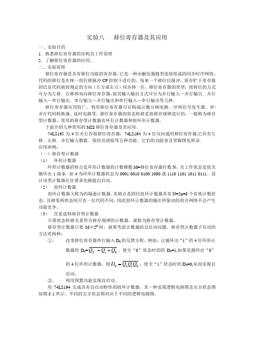
实验八 移位寄存器及其应用一、实验目的1.熟悉移位寄存器的结构及工作原理 2.了解移位寄存器的应用。
二、实验原理移位寄存器是具有移位功能的寄存器。
它是一种由触发器链型连续组成的同步时序网络。
代码的移位是在统一的位移脉冲CP 控制下进行的。
每来一个移位位脉冲,原存贮于寄存器的信息代码就按规定的方向(左方或右方)同步移一位。
移位寄存器的类型,按移位的方式可分为左移﹑右移和双向移位寄存器;按其输入输出方式可分为并行输入—并行输出﹑并行输入—串行输出﹑串行输入—并行输出和串行输入—串行输出等几种。
移位寄存器应用较广。
利用移位寄存器可以构成计数分频电路﹑序列信号发生器、串/并行代码转换器、延时电路等。
移位寄存器的状态转移是按移存规律进行的,一般称为移存型计数器。
常用的移存型计数器有环行计数器和扭环形计数器。
下面介绍几种常用的MSI 移位寄存器及其应用。
74LS195为4位并行存取移位寄存器;74LS194为4位双向通用移位寄存器,它具有左移﹑右移﹑并行输入数据﹑保持及清除等五种功能。
它们的功能表及管脚图见附录. 应用举例:(一)移存型计数器 (1) 环形计数器环形计数器的特点是环形计数器的计数模数M=移位寄存器位数N ,且工作状态是依次循环出1或0,如4为环形计数器状态为0001-0010-0100-1000或1110-1101-1011-0111。
设计该类计数器往往要求电路能自启动。
(2) 扭环计数器扭环计数器又称为约翰逊计数器。
其特点是四位扭环计数器具有N=2n=8个有效计数状态,且相邻两状态间只有一位代码不同,因此扭环计数器的输出所驱动的组合网络不会产生功能竞争。
(3) 任意进制移存型计数器只要状态转移关系符合移存规律的计数器,就称为移存型计数器。
移存型计数器只要M ≠2N 时,就要考虑计数器的自启动问题。
移存型计数器子启动的方法有两种:①、 改变移位寄存器串行输入D 0的反馈方程,例如:让循环出“1”的4位环形计数器的D 0=012Q Q Q ++,使全“0”状态时的的D 0=1;如果是循环出“0”的4位环形计数器,则0120Q Q Q D =,使全“1”状态时的D 0=0,从而实现自启动。
移位寄存器

实验报告4 移位寄存器实验原理:74194是一种典型的中规模集成移位寄存器, 由4个RS触发器和一些门电路构成的4位双向移位寄存器。
该移位寄存器具有左移、右移、并行输入数据、保持及异步清零5种功能。
其中A、B、C、D为并行数据输入端, QA、QB、QC、QD为并行数据输出端;SRSI为右移串行数据输入端, SLSI为左移串行数据输入端;S1.S0为模式控制端;CLRN为异步清零端;CLK为时钟脉冲输入端。
74194功能验证电路:波形图:End time: 1.0us period time:100.0 nsClk为时钟脉冲信号, clrn为清零端(低电平有效), s0为右移, s1为左移, sl、sr 分别表示左移右移的串行数据输入端。
Abcd表示并行数据输入端, Q_abcd表示并行数据输出端。
0000 右移补一10001000 清零00000000 左移补一00010001 左移补零00100010 右移补一10011001 右移补零0100当输入端随时钟的推移进行变化时, 仿真结果正确, 验证成功。
管脚分配:移位寄存器数码管显示电路图:74194用来并行移位, 4选1多路选择器用来选择74194的其中一位输出, vhdl7449用来将选中的一位转换成在数码管上表示时的段选。
Counter4产生选择信号, 然后74139(2-4译码器)就可以生成位选。
波形图:end time: 2.0 us priod time: Clk_s: 100.0ns clk_q: 10.0nsClk_s为段选时钟脉冲信号, Clk_q为位选时钟脉冲信号clrn为清零端(低电平有效), s0为右移, s1为左移, sl、sr分别表示左移右移的串行数据输入端。
din表示并行数据输入端, qbsg表示位数, q表示数码管上的段数。
到达第一个上升沿之前, 四位均为0, 在数码管上表示为“1111110”。
到达第一个上升沿后, 0010右移补一, 为1001, 在数码管上表示为“0110000, 1111110,111110,0110000”清零后, 四位均为0, 在数码管上表示为“1111110”。
- 1、下载文档前请自行甄别文档内容的完整性,平台不提供额外的编辑、内容补充、找答案等附加服务。
- 2、"仅部分预览"的文档,不可在线预览部分如存在完整性等问题,可反馈申请退款(可完整预览的文档不适用该条件!)。
- 3、如文档侵犯您的权益,请联系客服反馈,我们会尽快为您处理(人工客服工作时间:9:00-18:30)。
Shift registers1.0 IntroductionShift registers are a type of sequential logic circuit, mainly for storage of digital data. They are a group of flip-flops connected in a chain so that the output from one flip-flop becomes the input of the next flip-flop. Most of the registers possess no characteristic internal sequence of states. All flip-flop is driven by a common clock, and all are set or reset simultaneously.In these few lectures, the basic types of shift registers are studied, such as Serial In - Serial Out, Serial In - Parallel Out, Parallel In – Serial Out, Parallel In - Parallel Out, and bidirectional shift registers. A special form of counter - the shift register counter, is also introduced.Register:??A set of n flip-flops??Each flip-flop stores one bit??Two basic functions: data storage (Figure 1.2) and data movement (Figure 1.1).Shift Register:??A register that allows each of the flip-flops to pass the stored information to its adjacent neighbour??Figure 1.1 shows the basic data movement in shift registers. Counter:??A register that goes through a predetermined sequence of statesStorage Capacity:The storage capacity of a register is the total number of bits (1 or 0) of digital data it can retain. Each stage (flip flop) in a shift registerrepresents one bit of storage capacity. Therefore the number of stages in a register determines its storage capacity.Figure 1.2: The flip-flop as a storage element.2.0 Serial In - Serial Out Shift RegistersThe serial in/serial out shift register accepts data serially – that is, one bit at a time on a single line. It produces the stored information on its output also in serial form.2.1 Example: Basic four-bit shift registerFigure 2.1A basic four-bit shift register can be constructed using four D flip-flops, as shown in Figure 2.1.The operation of the circuit is as follows.??The register is first cleared, forcing all four outputs to zero.??The input data is then applied sequentially to the D input of the first flip-flop on the left (FF0).??During each clock pulse, one bit is transmitted from left to right.??Assume a data word to be 1001.??The least significant bit of the data has to be shifted through the register from FF0 to FF3.In order to get the data out of the register, they must be shifted out serially. This can be done destructively or non-destructively. For destructive readout, the original data is lost and at the end of the read cycle, all flip-flops are reset to zero.FF0 FF1 FF2 FF30 0 0 0 1001The data is loaded to the register when the control line is HIGH (ie WRITE). The data can be shifted out of the register when the control line is LOW (ie READ).Clear FF0 FF1 FF2 FF31001 0 0 0 0FF0 FF1 FF2 FF31 0 0 1 0000READ:FF0 FF1 FF2 FF31 0 0 1 1001Figure 2.2 illustrates entry of the four bits 1010 into the register. Figure 2.3 shows the four bits (1010) being serially shifted out of the register and replaced by all zeros.2.2 5-bit serial in/serial out shift registersFigure 2.4 illustrates entry of the five bits 11010 into the register.3.0 Serial In - Parallel Out Shift RegistersFor this kind of register, data bits are entered serially in the same manner as discussed in the last section. The difference is the way in which the data bits are taken out of the register. Once the data are stored, each bit appears on its respective output line, and all bits are available simultaneously. A construction of a four-bit serial in - parallel out register is shown below.In the table below, we can see how the four-bit binary number 1001 is shifted to the Q outputs of the register.Clear FF0 FF1 FF2 FF31001 0 0 0 01 0 0 00 1 0 00 0 1 01 0 0 13.1 An 8-bit serial in/parallel out shift register (74HC164) The 74HC164 is an example of an IC shift register having serial in/parallel out operation. The logic diagram and logic block are shown in Figure 3.1 (a),(b).4.0 Parallel In - Serial Out Shift RegistersA four-bit parallel in - serial out shift register is shown below. The circuit uses D flip-flops and NAND gates for entering data (ie writing) to the register.D0, D1, D2 and D3 are the parallel inputs, where D0 is the most significant bit and D3 is the least significant bit. To write data in, the mode control line is taken to LOW and the data is clocked in. The data can be shifted when the mode control line is HIGH as SHIFT is active high. The register performs right shift operation on the application of a clock pulse, as shown in the table below.Q0 Q1Q2Q3Clear 0 0 0 0Write 1 0 0 1Shift 1 0 0 11 1 0 0 11 1 1 0 011 1 1 1 0011 1 1 1 10014.1 8-bit Parallel Load Shift Register (74HC165)The 74HC165 is an example of an IC shift register that has a parallel in/serial out operation. It can also be operated as serial in/serial out. Figure 4.1 shows the logic diagram and logic symbol of 74HC165.Figure 4.1: the logic diagram and logic symbol of 74HC165.Figure 4.2: The timing diagram of 74HC165.5.0 Parallel In - Parallel Out Shift RegistersFor parallel in - parallel out shift registers, all data bits appear on the parallel outputs immediately following the simultaneous entry of the data bits. The following circuit is a four-bit parallel in - parallel out shift register constructed by D flip-flops.Figure 5.1The D's are the parallel inputs and the Q's are the parallel outputs. Once the register is clocked, all the data at the D inputs appear at the corresponding Q outputs simultaneously.5.1 4-bit Parallel-Access Shift Register (74HC195)The 74HC195 can be used for parallel in/parallel out operation, serial in/serial out and serial in/parallel out operations. Q3 is the output when it is used for parallel in/serial out operation.Figure 5.2: The 74LS195A 4-bit parallel access shift register6.0 Bidirectional Shift RegistersThe registers discussed so far involved only right shift operations. Each right shift operation has the effect of successively dividing the binary number by two. If the operation is reversed (left shift), this has the effect of multiplying the number by two. With suitable gating arrangement a serial shift register can perform both operations.A bidirectional, or reversible, shift register is one in which the data can be shift either left or right. A four-bit bidirectional shift register using D flip-flops is shown below.Here a set of NAND gates are configured as OR gates to select data inputs from the right or left adjacent bistables, as selected by the LEFT/RIGHT control line.Alternative Circuit:[Floyd]6.1 4-Bit Bidirectional Universal Shift Registers (74HC194) The 74HC194 is a universal bi-directional shift register. It has both serial and parallel input and output capability.[Floyd]Figure 6.1:The 74HC194 4-bit bi-directional universal shift register7.0 Shift Register CountersTwo of the most common types of shift register counters are introduced here: the Ring counter and the Johnson counter. They are basically shift registers with the serial outputs connected back to the serial inputs in order to produce particular sequences. These registers a re classified as counters because they exhibit a specified sequence of states.7.1 Ring CountersA ring counter is basically a circulating shift register in which the output of the most significant stage is fed back to the input of the least significant stage. The following is a 4-bit ring counter constructed from D flip-flops. The output of each stage is shifted into the next stage on the positive edge of a clock pulse. If the CLEAR signal is high, all the flip-flops except the first one FF0 are reset to 0. FF0 is preset to 1 instead.Since the count sequence has 4 distinct states, the counter can be considered as a mod-4 counter. Only 4 of the maximum 16 states are used, making ring counters very inefficient in terms of state usage. But the major advantage of a ring counter over a binary counter is that it is self-decoding. No extra decoding circuit is needed to determine what state the counter is in.7.1.1 Example: A 10-bit Ring Counter [Flyod]Figure 7.1: 10-bit ring counter & its sequence7.2 Johnson CountersJohnson counters are a variation of standard ring counters, with the inverted output of the last stage fed back to the input of the first stage. They are also known as twisted ring counters. An n-stage Johnson counter yields a count sequence of length 2n, so it may be considered to be a mod-2n counter. The circuit below shows a 4-bit Johnson counter. The state sequence for the counter is given in the table .??Again, the apparent disadvantage of this counter is that the maximum available states are not fully utilized. Only eight of the sixteen states are being used.??Beware that for both the Ring and the Johnson counter must initially be forced into a valid state in the count sequence because they operate on a subset of the available number of states. Otherwise, the ideal sequence will not be followed.7.2.1 Example: 5 bit Johnson Counter[Flyod]Figure 7.3: 5-bit Johnson Counter, its sequence and waveform8.0 ApplicationsShift registers can be found in many applications. Here is a list of a few.??To produce time delayThe serial in -serial out shift register can be used as a time delay device. The amount of delay can be controlled by:1. the number of stages in the register2. the clock frequencyFigure 8.1: The shift register as a time-delay device.??To simplify combinational logicThe ring counter technique can be effectively utilized to implement synchronous sequential circuits. A major problem in the realization of sequential circuits is the assignment of binary codes to the internal states of the circuit in order to reduce the complexity of circuits required. By assigning one flip-flop to one internal state, it is possible to simplify the combinational logic required to realize the complete sequential circuit. When the circuit is in a particular state, the flip-flop corresponding to that state is set to HIGH and all other flip-flops remain LOW.??To convert serial data to parallel dataA computer or microprocessor-based system commonly requires incoming data to be in parallel format. But frequently, these systems must communicate with external devices that send or receive serial data. So, serial-to-parallel conversion is required. As shown in the previous sections, a serial in - parallel out register can achieve this.Figure 8.2: Simplified logic diagram of a serial-to-parallel converter。